dedication - trs-80 color computer archive
TRANSCRIPT


THE
MC6809 COOKBOOK
by carl d. warren
Red text is the original error correction in the book For corrections to the PDF or owners of copyright of the book want to remove it, please contact by [email protected]. This PDF is made only for the preservation of information of the color computer, not to affect the copyright, will always be preferable to the original purchase, the PDF also aids in searches in the book. Or if you can not easily acquire on the market, as in my case in Venezuela. Some pages were scan at 300 DPI (if font small) but most are 200 DPI, and ABBYY FineReader 8.0 Professional Edition

Dedication For ACE
No questions asked
TAB TAB BOOKS Inc. BLUE RIDGE SUMMIT. PA. 17214
FIRST EDITION
SECOND PRINTING
Copyright © 1980 by TAB BOOKS Inc.
Printed in the United States of America
Reproduction or publication of the content in any manner, without express permission of the publisher, is prohibited. No liability is assumed with respect to the use of the information herein.
Library of Congress Cataloging in Publication Data
Warren, Carl D The MC6809 cookbook.
Includes index. 1. Motorola 6809 (Computer) I.Title
QA76.8.M67W37 001.64 80-23359 ISBN 0-8306-9683-0 ISBN 0-8306-1209-2 (pbk.)
is a trademark of Motorola Inc.

Contents Acknowledgments 6 Preface 7
1 General Descriptions 9 Introduction to the 6809—Basics of the 6809 µP—High Level Language Processor—Changed Configuration—The Right Nomenclature—Variety in Clocks—6809 MPU Signal Description—Pulling the Schmitt-Trigger—Tracing the Interrupt—Establishing a System
2 6809 µP Software Architecture 25 The Software Tale—Registers, Pointers and Things—Condition Codes Are Special—6800/6809 Software Incompatibilities-Equivalencies—Performance Summary
3 Addressing Modes 37 Basic Concepts—Inherent Addressing Mode—Immediate Addressing—Extended Addressing—Direct Addressing— Register Addressing—Indexed Addressing—Indexed Indirect-Relative Addressing—Summary
4 Into the Instruction Set 56 Push-Pull and Address It—Individual instructions
5 MEK6809EA Assembler 112 Basics of the Assembler—Typical Requirements— Expressions—Symbols—Assembler Listing
6 Implementation of VTL-09 118 Direct and Program Statements—Preliminary Concepts— Arithmetic Operations
Appendix A Motorola 6809D4 134 Highlights—Model Types—Expansion—Software Features— Added D4B Software Features—MEK6809D4 Description— MEK68KPD Description—Sample Programs
Appendix B Hexadecimal Values of Machine Codes 148
Appendix C Programmer's Card 153
Appendix D Instruction Index 169
Index 176
Acknowledgments
When any work such as this is embarked upon, it requires a massive amount of support from a variety of sources. It was necessary to rely upon the suggestions and resources of a number of people and companies. Among these people are; Ron Denchfield of AMI who supplied, most of the figures and the programmer's card, Tim Ahrens, Bill Clendinning and Irwin Carroll of Motorola, who provided various tables and important suggestions, along with the 6809D4 evaluation unit.
Since this book is about computer technology, it is only appropriate that it was created with aid of a computer. The manuscript was prepared on a Heath H-89 microcomputer, and printed on an Epson TX-80 dot matrix printer. The software that was used consisted of a variety of products. Among these were the editor and text formatter available from the Heath users' group (HUG), the PIE editor from the Software Toolworks, and a very special program called COPY that permits interchanging software created under HDOS to CP/M compatible files. This unique piece of magic was created by Bob Mathias, a genius of our times. Other software was supplied courtesy of Tony Gold at Lifeboat Assoc. These consisted of Organic software's Textwriter III for text formatting and Digital Research's CP/M optimized for a 4200H base.
Special thanks is reserved for the finest managing editor in the magazine industry today, Jordan Backler. It is because of his suggestions, coupled with those from fellow EDN editors Bob Peterson, and Ed Teja, that this work is as concise as it is.
My wife Anne and daughter Tami played probably the most important part in the creation of this book—putting up with the writing process and making sure the coffee was always available.
6

Preface As a result of the profliferation of microprocessors (µP), since 1977 hardware and software designers have been able to extend their capabilities in terms of creating useful products for everyday life. Each day, new processor introductions are opening up even more exciting vistas. Unfortunately, there is a problem associated with the introduction of the newer devices: how to correctly use them for maximum benefit and efficiency.
This book, like many of its type, attempts to give the engineer or technician an expert command of the fundamentals of the 6809 microprocessor (µP), and the basic skills for writing 6809 assembly language level code. In systematic fashion, it proceeds from analysis of the microprocessors design to its important electrical characteristics. It continues with discussion on matters like internal logic, comparison to the 6800, interfacing to peripherals, software architecture, addressing techniques and the instruction set. It concludes with advice on how to build or make use of existing 6809 based systems. Further enhancing The MC6809 Cookbook's usefulness is the inclusion of a programmer's card, provided courtesy of American Microsystems Inc. (AMI).
The MC6809 Cookbook may be studied as a course, proceeding from the simple to the more complex. However, it should be more appropriate viewed as a reference source to be called upon as necessary. Therefore, I have kept the idea of a compact and concise reference work utmost in my mind while creating this book. As a
7

result of this goal, the diversified contents are readily identifiable to facilitate the finding of specific principles or functions associated with the 6809 µP.
The MC6809 Cookbook aims to be comprehensive without being cumbersome. It seeks in all areas to be exact, clear and succinct.
Throughout this book, µP, and µC are used to mean microprocessor and microcomputer, respectively. These are stylistic nuances used at EDN magazine, and permit brevity without being imprecise.
carl d. warren
8

General Descriptions
The 6809 /xP, developed by Motorola and second sourced by American Microsystems Inc. (AMI), is a high performance mul-tifaceted device. It is considered by many industry observers and Motorola to be the interim processor between 8-bit and 16-bit devices. The general design philosophy of the device seems to support this conjecture in that it permits the handling of 16-bit registers with powerful instructions.
INTRODUCTION TO THE 6809
The 6809 µP is unique because it represents an upward growth device from the ubiquitous 6800 (µP. This upward growth is in the form of software compatibility, at the source code level, and apparent similar operation of the two devices.
As a result of these similarities, it is possible to design the 6809 µP into a variety of applications. Among these applications are process control, automobile system monitoring, television sets, intelligent terminals and other devices more far reaching than this book could even begin to mention. As an example of the use of the 6809 µP was recently incorporated into what will more than likely become the small computer system of the decade, the Radio Shack TRS-S0 Videotex (Fig. 1-1). This unit not only uses the 6809 /xP, but the entire spectrum of Motorola support and peripheral chips. The point is that it shows the flexibility of the 6809 µP.
9

Fig. 1-1. Incorporating the 6809 µP in concert with a host of Motorola compatible peripheral device chips, the Radio Shack TRS-80 Videotex is designed to transform the home television and telephone into a high-powered communication system (courtesy of Radio Shack).
Flexibility and ease of system integration are important features of the 6809 µP, but are only representative of just a minor portion of the processor's capability. Throughout the rest of this book, you will be introduced to the specific features and functions of the processor and given sufficient information to make it work for you.
BASICS OF THE 6809 µP
The 6809 µP is an 8-bit NMOS device. With all the different mnemonics around—buzz words—it can be extremely difficult to figure out what someone is talking about in device types. For example, I say the 6809 µP is an NMOS device which it most surely is. Metal Oxide Substrate (MOS) technology is a method of creating integrated circuits (ICs); the N or P indicates the type of channel the device has built into it and does, in fact, refer to negative or positive. But for the purposes of this book, suffice it to say the device is NMOS. An NMOS device exhibits an electron mobility about 2.4 times that of PMOS. Consequently, the NMOS device outperforms similar PMOS devices in speed and power. This means more power to you, the designer, in a smaller and in most cases less expensive package.
10

The processor is designed, according to Motorola engineers, for real-time and character manipulation programming. This design philosophy implies that the device is ideal for such applications as real time, or event, data collection. Applications such as this require that the processor work in concert with data acquisition probes like thermocouples, strain gauges or flow sensors to name a few. The 6809 µP offers the important characteristics of being able to respond quickly enough to handle the influx of data from this type of device.
The character oriented capability of the 6809 µP makes it an excellent choice for word processing applications. In this type of application, ASCII data is manipulated in several ways to create useful output data. Word processing implies that the µP must work with a variety of peripheral devices, a functional plus of all 68XX type parts. HIGH LEVEL LANGUAGE PROCESSOR
Another feature of the 6809, µP is that it is a byte-oriented device rather than operating on each bit of the 16 available on the address bus. This single characteristic enhances the processor's ability to function, with efficiency, as a high-level language computer.
The reason this processor, or any processor for that matter, works better as a high level language processor if it is byte-oriented is that a byte is 8 bits long. It is directly equatable to a character of some type, for example the letter A. High level language like COBOL and FORTRAN work by comparing block structures made up of characters to determine a task. Bit-oriented devices must first build a byte from individual bits, store it in a register and then permit the language instruction to perform some work or comparison. The byte-oriented device makes the assumption that registers are filled with bytes, thus speeding up execution times. This fact does not preclude bit operations that must take place in math functions.
Although the 6809 µP is not a pin-for-pin replacement of the 6800, it is not all that different in the sense of compatible functions and software. For example, the 6800 µP exhibited one stack pointer; the 6809 has two. The 6809 µP has two index registers as opposed to the single index register of the 6800. In relationship to the improved indexing capability of the device, both the stack pointers and program counter can be indexed. This feature makes it. much easier for the programmer to manipulate data held in the processor's registers.
11
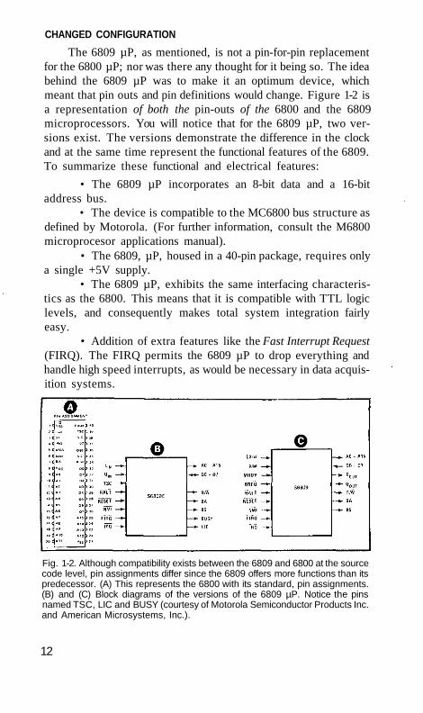
CHANGED CONFIGURATION
The 6809 µP, as mentioned, is not a pin-for-pin replacement for the 6800 µP; nor was there any thought for it being so. The idea behind the 6809 µP was to make it an optimum device, which meant that pin outs and pin definitions would change. Figure 1-2 is a representation of both the pin-outs of the 6800 and the 6809 microprocessors. You will notice that for the 6809 µP, two versions exist. The versions demonstrate the difference in the clock and at the same time represent the functional features of the 6809. To summarize these functional and electrical features:
• The 6809 µP incorporates an 8-bit data and a 16-bit address bus.
• The device is compatible to the MC6800 bus structure as defined by Motorola. (For further information, consult the M6800 microprocesor applications manual).
• The 6809, µP, housed in a 40-pin package, requires only a single +5V supply.
• The 6809 µP, exhibits the same interfacing characteristics as the 6800. This means that it is compatible with TTL logic levels, and consequently makes total system integration fairly easy.
• Addition of extra features like the Fast Interrupt Request (FIRQ). The FIRQ permits the 6809 µP to drop everything and handle high speed interrupts, as would be necessary in data acquisition systems.
Fig. 1-2. Although compatibility exists between the 6809 and 6800 at the source code level, pin assignments differ since the 6809 offers more functions than its predecessor. (A) This represents the 6800 with its standard, pin assignments. (B) and (C) Block diagrams of the versions of the 6809 µP. Notice the pins named TSC, LIC and BUSY (courtesy of Motorola Semiconductor Products Inc. and American Microsystems, Inc.).
12

• Vectored interrupts allow the 6809 µP to locate an interrupt servicing routine within a minimum amount of time, and return back to the starting location without destroying the current data.
• The 6809 µP incorporates an onboard oscillator which is four times the input frequency of the crystal. The 6809E version features an external clock. See Fig. 1-3. This allows the 6809 µP to sync with an external clocking source such as that being generated by a clock source from another system.
• The 6809 MPU has two memory functions not found with the 6800: MRDY that extends data access times for use with slow memory, and DMA/BREQ that permits quick access to the bus for Direct Memory Access (DMA) and memory refresh.
The electrical differences in the two versions are shown in Figs. 1-3A and 1-3B. Basically, the two versions of the 6809 µP are the same, with the exception of the clocking mode. Table 1-1 defines the Read/Write for each version of the microprocessor. Table 1-2 lists the electrical characteristics of the processor.
THE RIGHT NOMENCLATURE As you proceed through this book, you will notice reference to
a part preceded by an S. This nomenclature defines the part as being from AMI. When the device being referred to is a Motorola part, the number is preceded by an M or MC. However, for the sake of clarity I have adopted the generic term—6809. There are some tables and figures in this book that do make reference to the specific manufacturers' devices.
VARIETY IN CLOCKS
The 6809 µP incorporates the choice of two clock functions. The basic 6809 processor exhibits an internal clock (oscillator). To make use of this clock, an external crystal is connected between EXTAL and XTAL pins 39 and 38. Netting or filter 0.01 disc ceramic capacitors are on either side to the system ground (Fig. 1-4). When the 6809 is in this configuration, a synchronization signal is available at the E/out terminal (pin 34). This available signal can be used as the system clock with all other devices in sync with it.
The output that is available on pin 34 is at the basic processor frequency and for most applications is connected to the Enable (02) input of 6800 peripheral devices, as shown in Fig. 1-5. This simplification of the clocking system, with 6800 family compatibility, eases system design and integration.
13
Fig. 1-3. Providing flexibility to the system designer, the 6809 µP is built with either an internal oscillator (A) or for use with an external clock (B) (courtesy of American Microsystems, Inc.).
Besides the timing signals discussed, another signal called the Quadrature output (Q/out) is available. The purpose of this signal is to signify that addresses and data are stable. This stability tells the system that operations have settled down and something else can take place.
Table 1-1. Read/Write Timing (courtesy of American Microsystems, Inc. and Motorola Semiconductor Products Inc.).
14
Table 1-2. Electrical Characteristics (courtesy American Microsystems, Inc. and Motorola Semiconductor Products Inc.).
The external clock version, indicated by an E, requires that an external clock source be implemented. This external clock must generate an output at the MPU frequency. The timing signal E is similar to the 6800 bus timing signal 02; Q is a quadrature clock, signal which leads E. This quadrature signal has no parallel on the 6800. The importance of these signals are that addresses from the MPU will be valid with the leading edge of Q (Fig. 1-6). Data is latched on the falling edge of E.
You will notice from Fig. 1-3 that the external clock version of the 6809, the BREQ input, is replaced by a tri-state (TSC) control. This control serves to place the address and R/W in the high
Fig. 1-4. The clock on the 6809 is invoked by tying pins 38 and 39 together via a crystal and filter capacitors (courtesy American Microsystems, inc. and Motorola Semiconductor Products Inc.).
15

Fig. 1-5. Interfacing the 6809 µP to other devices is easy by taking the output from pin 34 and tying it to the chip enable pin of the peripheral chip. In this figure, the processor is tied to RAM, ROM and output devices. Pay particular attention to the direction of the data on the data bus. The output from 34 is tied to the chip enable of the output latch and input buffer.
cycle of any instruction. This signifies that the next instruction cycle is the opcode fetch and acts like a pipeline fetch, thus improving processing throughout. The processor BUSY signal facilitates multiprocessor applications by allowing the designer to
Fig. 1-6. E/Q relationship (courtesy American Microsystems, Inc. and Motorola Semiconductor Products Inc.).
16
16-BIT ADDRESS BUS
ADDRESS DECODER
ADDRESS DECODER
INPUT DEVICE
ADDRESS DECODER
ADRESS
DECODER OUTPUT
DEVICE
CHIP ENABLE
RAM
CHIP ENABLE ROM
OUTPUT LATCHES
CHIP ENABLE
INPUT SUFFER CHIP ENABLE
6809 MPU
8 BIT DATA BUS 34

impedance state for DMA or memory refresh. The E and Q pins are replaced by two status outputs: Last Instruction Cycle (LIC) and processor busy signal (BUSY). The LIC is activated during the last insure that flags being modified by one processor are not accessed by another simultaneously.
The 6809 µP, in normal operation, fetches an instruction from memory and then executes the requested function. This operational function begins when the processor is started—RESET— and repeated until forced to cease. This stopping of the operation can be from a multitude of sources including interrupts, hard and soft, or via a special instruction that permits the processor to HALT but also save the contents of the registers—that is, waiting to proceed without impacting the computing ability of the processor.
6809 MPU SIGNAL DESCRIPTION
This section describes the functional purposes of the pins available on the 6809 µP.The reason, is to create a solid foundation for the chapters on addressing and the instruction set.
The information contained in this section is, in most cases, directly from AMI literature. I have attempted, where necessary, to further clarify or amplify upon those items that seem vague.
Power (Vss Vcc) Pins 1 And 7. Two pins are used to supply power to the part: V is ground, or 0 volts, while Vcc is +5V with a 5% tolerance. This holds true whether the device is of the internal or external clock variety (Fig. 1-7).
Address Bus (A0 - A15) Pins 8-23. Sixteen pins are used to output address information from the MPU onto the address bus. When the processor does not require the bus, for a data transfer, it will output address FFFF16, R/ = 1 and BS = 0 (Table 1-3). Addresses are valid on the rising edge of Q. All address bus drivers are made high-impedance when output Bus Available (BA) is high. Each pin will drive one Schottky TTL load and typically 90pF (Fig. 1-7).
Data Bus (D0-D7) (Pins 24-31). The eight pins, designated for data, provide communication with the system bidirectional data bus. Each pin will drive one Schottky TTL load and typically 130pF (Fig. 1-7).
Read/Write (R/W) Pin 32. This signal indicates the direction of the data transfer on the data bus. A low indicates that the
17

Fig. 1-7. (A) Block diagram. (B) Pin configuration (courtesy of American Microsystems, Inc. and Motorola Semiconductor Products Inc.).
MPU is writing data onto the data bus. R/ is made high impedance when BA is high. R/ is valid on the rising edge of Q.
Pin 37 . A low level on this Schmitt trigger* input for greater than one bus cycle will the MPU. The RESET vectors are fetched from locations FFFE16 and FFFF16 when interrupt acknowledge is true BABS=1). During initial power on, the Reset line should be held low until the clock oscillator is fully operational.
Because the 6809 µP Reset pin has a Schmitt-trigger input with a threshold voltage higher than that of standard peripherals, a
Table 1-3. MPU State (courtesy of American Microsystems, Inc.).
MPU State
BA
o o 1 1
BS
0 1 0 1
Normal (running) Interrupt Acknowledge SYNC Acknowledge HALT or Bus grant
18

simple R/C network may be used to reset the entire system. This higher threshold voltage insures that all peripherals are out of the reset state before the processor.
PULLING THE SCH MITT-TRIGGER
A Schmitt-trigger is a special type of flip-flop circuit that permits feedback and is sometimes referred to as a regenerative switching circuit, having two stable output states. The Schmitt-trigger is frequently used in timing circuits to mark the instant when an input voltage reaches the trigger level, converting a sinusoidal input voltage into a pulse train at the output. Since it is not within scope of this book to provide complete explanations of flip-flops, I recommend Electronic Circuits Digital and Analog, by Charles A. Holt, John Wiley and Sons, New York.
HALT—Pin 40 . A low level on this input pin will cause the MPU to stop running at the end of the present instruction and remain halted indefinitely without loss of data. When halted, the BA output is driven high indicating the buses are high-impedance. BS is also high which indicates the processor is in the Halt or Bus Grant State. While halted, the MPU will not respond to external real-time requests although will always be accepted and NMI or RESET will be latched for later response. During the HALT state Q and E continue to run normally. If the MPU is not running a halted state (BA and BS = 1) can be achieved by pulling HALT low while
is still low. If and are both pulled low, the processor will reach the last cycle of the instruction (by reverse cycle stealing) where the machine will then become halted (Fig. 1-8).
Bus Available. Bus Status (BA, BS) Pins 5 and 6. The Bus Available output is an indication of an internal control signal which makes the MOS buses of the MPU high-impedance. This signal does not imply that the bus will be available for more than one cycle. When BA goes low, an additional dead cycle will elapse before the MPU acquires the bus. The bus status output signal, when decoded with BA, represents the MPU state (valid with leading edge of Q).
TRACING THE INTERRUPT
When an interrupt occurs, the processor must respond in some manner. The 6809 µ,P responds by going to a location in memory and executing a specific routine. In all cases, the proces-
19
Fig. 1-8. HALT and single instruction execution for system debug (courtesy of American Microsystems, Inc. and Motorola Semiconductor Products Inc.).
sor generates a signal called an interrupt Acknowledge. It is indicated during both cycles of a hardware-vector-fetch
SWI, SWI2, SWI3). This signal, plus decoding of the lower 4 address lines, can provide the user with an indication of which interrupt level is being serviced and allow vectoring by device, as shown in Table 1-4.
Table 1-4. Memory Map for Interrupt Vectors (courtesy of American Microsystems, Inc.).
Memory Map for Interrupt Vectors
Memory Map for Vector Location
MS
FFFE FFFC FFFA FFF8 FFF6 FFF4 FFF2 FFFO
LS
FFFF FFFD FFFB FFF9 FFF7 FFF5 FFF3 FFF1
Interrupt Vector Description
SWI
SWI2 SWI3
Reserved
20

Other signals that play an important role either during an interrupt condition or HALT condition are Sync acknowledge and
Halt/Bus grant (Fig. 1-9). The Sync acknowledge is indicated while the MPU is waiting for external synchronization on an interrupt line. Halt/Bus Grant is true when the 6809 µP is in a or Bus Grant condition, as explained previously under HALT.
Nonmaskable Interrupt Pin 2. The Nonmaskable Interrupt pin is very similar to the pin 3, except that the interrupt input is nonmaskable from the MPU. This means that a program cannot inhibit the interrupt, and it has a higher priority than or or for that matter of software interrupts (Fig. 1-10).
The is invoked when a negative wedge is input on the pin. When recognized, the entire machine state is saved on the hardware stack. However, once the machine is reset, the is not recognized until the first program load of the Hardware Stack Pointer (S). The pulse width of low must be at least one E cycle. If the input does not meet the minimum set up with respect Q, the interrupt will not be recognized until the next cycle.
Fast-Interrupt Request Pin 4. It is unique to the 6809 µP. When a low level signal is detected at this pin, a fast interrupt sequence, provided its mask bit (F) in the CC is clear, will be initiated. The has priority over the standard Interrupt Request and is fast in the sense that it stacks only the contents of the condition code register and the program counter. When
Fig. 1 -9. SYNC timing (courtesy of American Microsystems, Inc., and Motorola Semiconductor Products Inc.).
21

used, the interrupt service routine should clear the source of the interrupt before doing a Return from Interrupt (RTI). The timing for this interrupt is shown in Fig. 1-10A.
Interrupt Request Pin 3. When this line is forced low, from some external device, the MPU will complete the instruction it is executing and go into the interrupt sequence. This is no different than for the 6800 µP. The has a lower priority than
, but the servicing routine should clear the source of the interrupt before returning to the calling routine (Fig. 1-10B).
When is invoked, the contents of the index register, the program counter, accumulators and condition code register will be stored on the stack. The I bit in the condition code register will be set to a 1 so that no further interrupts may occur, or at least until this one is serviced. As shown in Table 1-4, the MPU will nowload the contents of FFF816 and FFF916 into the program counter and vector the program to execute the interrupt routine pointed to by these locations. After an RTI is encountered, the MPU will return to its initial state.
Fig. 1-10. (A) interrupt timing. (B) and interrupt timing (courtesy of American Microsystems, Inc. and Motorola Semiconductor Products Inc.).
22
Fig. 1-11. MRDY timing (courtesy of American Microsystems, inc. and Motorola Semiconductor Products Inc.).
EXTAL, XTAL Pins 38 , 39 . These input pins are used to connect the on-chip oscillator to an external parallel-resonant crystal (Fig. 1-4). The pin labeled EXTAL may be used as TTL level input for external timing by grounding XTAL. The crystal or external frequency is 4 times the bus frequency which is shown in Fig. 1-4.
E, Q Pins 34, 35. Here you can see some specific similarities between the 6800 µP and the 6809. E is similar to the 6800 bus timing signal Q2; Q is a quadrature clock signal which leads E. Q has no parallel on the 6800. Addresses from the MPU will be valid with the leading edge of Q. Data is latched on the falling edge of E.
MRDY Pin 36. This input control signal allows stretching of E to extend data-access time. When MRDY is high, E will be in normal operation. When MRDY is low, E may be stretched integral multiples of quarter (¼) bus cycles, thus allowing interface to slow memories as shown in Figs. 1-11. A maximum stretch is 10 µsec. During non-valid memory accesses ( cycles), MRDY has no effect on stretching E. This inhibits slowing the processor speed during don't care bus accesses.
Pin 33. The DMA/BREQ input provides a method of suspending execution and acquiring the MPU bus for another use. Typical uses include DMA and dynamic memory refresh.
Transition of should occur during Q. A low level on this pin will stop instruction execution at the end of the current cycle. The MPU will acknowledge by setting BA and BS to a one. The requesting device will now have up to 15 bus cycles before the MPU retrieves the bus cycle with a leading and trailing dead cycle.
23
ESTABLISHING A SYSTEM
Now that you have a resonable understanding of the hardware side of the 6809 µP, you can build a working unit. All that is required is the 6809, some memory, power and form of display.
A typical system—the Motorola 6809D4 unit—is discussed in Appendix A. But the most important element behind the processor is not the hardware but rather how to program it. In the next chapter, the basic software architecture of the device will be introduced, followed by the various addressing techniques in Chapter 3 and finally the instruction set in Chapter 4.
24

6809 µP Software Architecture Software development entails the understanding of several disciplines—specifically hardware logic as it relates to the hardware, mathematics and general logic flow. Interestingly enough, the software engineer doesn't really need to have an in-depth understanding of the electrical characteristics of the processor he is programming, unless of course original system software development is the goal.
However, whether the goal is system software design or developing specific utility ware, the software architecture of the device must be understood.
THE SOFTWARE TALE
The 6809 µP is, as stated in Chapter 1, an upward growth device from the 6800 µP. Specifically, the 6809 adds three registers to the set available in the 6800. These include a direct page register, the user stack pointer and a second index register. These additional registers make the device extremely flexible, but the 6809 offers even other software features:
—Two 8-bit accumulators —Two 16-bit index registers. —Two 16-bit stack pointers with index capability. —The previously mentioned programmable direct page regis
ter. —59 instruction mnemonics (see Chapter 4).
25

—268 opcodes. — 1464 instructions with different addressing modes. —8x8 unsigned multiply. — 16-bit arithmetic: load, store, add, subtract and compare. —Powerful Push/Pull instructions. —Powerful register transfers and exchanges. —Powerful address-manipulation instructions. —Extended-range long branches.
As you can see, the device is extremely flexible and offers the software designer a great deal of power in a microprocessor. Figure 2-1 is the basic programming model for the 6809 µP. You will notice that the X and Y index registers are 16-bits wide, and the U and S stack pointers are also 16-bits. The interesting register is made up of two 8-bit registers, A and B, which together make up D. It is within these three registers—accumulators—that most of the processor's work will be done. The direct page and condition code registers are 8-bits wide and provide programming enchancement that will be explained later.
The general architecture of the device supports software techniques such as position-independent code, structured high level-subroutined code, multi-task and multi-processor operations, development and operation of stack oriented compiler instructions, and the important facilities of re-entrancy and recursion, both important facets of software for high-level language use
Fig. 2-1. Programming model of the microprocessing unit (courtesy of American Microsystems, Inc.).
26

or real-time data acquisition. Now that you know all of the good things that the software architecture behind the 6809 is supposed to provide, you are probably anxious for a more in-depth explanation of the programming model.
REGISTERS, POINTERS AND THINGS
Taking a look at Fig. 2-1, you can see that within the structure there are the X and Y 16-bit index registers. These are also referred to as the pointer registers.
The index registers are used in the indexed mode of addressing. The 16-bit address in either the X and Y register is used to point to data directly, or it may be modified by an optional constant or register offset. The X and Y registers are equivalent in usage and consequently support the same instructions. These registers may be used to implement software stacks, queues and buffers.
Stack pointers U and S, shown in Fig. 2-1, can also be used as index registers, but they serve very specific purposes in processing. The Hardware Stack Pointer (S) is used by the processor during subroutine calls and interrupts.The difference between this stack pointer and that on the 6800 µP is that it points to the top of the stack rather than the next free location (Table 2-1).
The User Stack Pointer (U) is for use by you, the programmer. This stack pointer permits you to pass arguments to and from subroutines with ease. This facility coupled with the hardware stack pointer makes the 6809 µP and ideal stack processor and enhances its functioning as a higher level language processor. Because the architecture of the U and S pointers are, as previously indicated, the same as the X and Y registers, they also support the same instructions plus the PUSH and PULL stack controls.
The next register is the Program Counter (PC). This register is 16-bits and is used by the processor to point to the address of the next instruction to be executed by the processor. Relative addressing is provided allowing the PC to be used like an index register in some situations. Limited index-mode addressing is available, but functions such as auto increment and decrement are not.
In operation, each instruction used by the processor assumes that the PC points one location past the last byte Of the op code— as it would after decoding the instruction. Consequently, as additional bytes are used by the instruction, the PC always points to the next unused byte.
The next registers, A, B and D accumulators, are made up of two 8-bit registers as shown by Fig. 2-1. The A and B registers are
27
Table 2-1. 6809 µP Push/Pull and Interrupt Stacking Order.
general purpose accumulators which are used for arithmetic calculations and manipulation of byte size data. What makes this pair unique is that certain instructions concatenate A and B to form the 16-bit register D, with the contents of A being the most significant byte.
The Direct Page register (DP) defines the most significant (MS) byte to be used in the direct mode of addressing. The DP is concatenated with the byte following the direct mode op code to form a 16-bit effective address. The contents of this register appear at the higher address output (A8-A15) during direct addressing instruction execution. This permits the use of the direct mode anywhere in memory. To maintain 6800 compatibility, all bits are initialized to $00 on Reset of the processor. CONDITION CODES ARE SPECIAL
The final register in the programming model of Fig. 2-1 is the condition code register (CC). Figure 2-2 is the format for this 8-bit
28
PULL FROM STACK TOP OF STACK PUSH ONTO STACK
SP(or US)
PUSH ORDER

Fig. 2-2. Condition code register format (courtesyAmerican Microsystems, Inc.).
register. Notice that each bit is defined and based on the condition—toggle 0 or 1—which defines the operation state of the processor and is always nice to know.
Each bit within the register performs a specific task. For example, bits 0-3 and 5 are set as the result of instructions that manipulate data in some way. The actual definitions of each bit follows.
Bit 0 (C)
Bit 0 is the Carry Flag, and is usually the carry from the binary Arithmetic Logic Unit (ALU). Specifically, the C flag is generated by the binary carry from the Most Significant Bit (MSB) of the operations (ADC, ADD). Furthermore, C is used to represent a "borrow" from subtract-like instructions (CMP, NEG, SUB, SBC). Only arithmetic operations affect C.
Bit 1 (V)
Bit 1 is the overflow flag and is set to a one by an operation which causes a signed two's complement arithmetic overflow. This overflow is detected in an operation in which the carry from the MSB in the ALU does not match the carry from the MSB-1. Loads, stores and logical operations set V.
Two's Complement
If you have advanced to this point in the book and aren't sure what two's complement is, you may have a problem. I would suggest that you obtain a copy of "Basic Microprocessor and the 6800," by Ron Bishop, Hayden Book Co., 1979. You might also consider the Heath course on microprocessors. Both are excellent sources for explaining this concept, which is important if you wish
29
CARRY
OVERFLOW
ZERO
SIGN FLAG
IRQ MASK
HALF CARRY
FIRQ MASK
ENTIRE STATE FLAG

to understand what you are doing. Should you know what two's complement is all about but can't quite get a picture in your mind, this note will serve to refresh your memory—no pun intended.
The two's complement is the method used to represent signed numbers in microprocessors. Positive numbers, in this system, use the same bit pattern for all values up to decimal +127. Negative numbers are represented as the two's complement of positive numbers.
To find the two's complement of a number, you first take the one's complement and then add one. The one's complement is formed by changing all the 0s to 1s and all the 1s to 0s. Invert all the bits. For example, the decimal number 10 is 00001010 in binary. If the number is positive (°10), you follow this procedure.
11110110 this now represents - 1 0
determines the sign when set—negative Bit 2 (Z)
Bit 2 is the zero flag and is set to a one if the result of the previous operation was identically zero. Loads, stores, logical and arithmetic operations set Z. Bit 3 (N)
Bit 3 is the negative flag, which obtains exactly the MSB value of the result of the preceding operation. Thus, a negative two's complement result will leave N set to a one. Loads, stores, logical and arithmetic operations all set N. If a two's complement overflow occurs, the sign of the result (and the N-flag) will be incorrect. Therefore, two's, compliment branches use the expression (N + V) to obtain an always valid sign result. Bit 4 (I)
This is the Interrupt Request (IRQ) mask bit. The processor will noi recognize interrupts from the IRQ line if this bit is set to a one. NMI, FIRQ, IRQ, RESET and SWI all set I to a one. However, SWI2 and SWI3 do not affect I. Bit 5 (H)
This bit is used to indicate a carry from bit 3 in the ALU as a result of an 8-bit addition only (ADC or ADD). This bit is used by the DAA instruction to perform a BCD decimal add adjust opera-
30
one's complement
two's complement
00001010 invert 11110101
add one

tion. The state of this flag is undefined in all subtract-like instructions. Bit 6 (F)
This bit is associated with the Fast Interrupt Request (FIRQ). If this bit is set, the processor will not recognize interrupts from the FIRQ line. NMI, FIRQ, SWI and all set F to a one. IRQ, SWI2 and SWI3 do not affect F. Bit 7 (E)
This bit (7) is reserved for indicating the state of the ENTIRE registers. It shows when the processor is stacked or the subset state (PC or CC) is being stacked. E is used by the Return from Interrupt (RTI) instruction to determine the extent of the unstack-ing. This function allows some interrupt handling routines which work with both fast and slow interrupts. FIRQ will clear E while IRQ, NMI, SWI, SWI2 and SWI3 will set E before stacking. The E bit associated with the saved registers is in the E flag position in the CC of the stacked state. Interrupts and the Condition Codes
When the 6809 accepts an interrupt, it will set the E flag bit 7 and save the entire machine state. Furthermore, the I mask bit 4 will be set to blank out the present and further IRQ interrupts. Once the interrupt is cleared, you can reset the I mask bit to permit multiple-level IRQ interrupts. When the IRQ occurs, the F mask bit 6 is not affected which means that an FIRQ interrupt can supersede the current IRQ interrupt. The machine state is recovered by the RTI instruction.
When an FIRQ interrupt is accepted, the E flag is cleared and the submachine state (return address and CC) is saved. The I and F bits are set to mask out further interrupts. Again, I and F can be reset to permit multiple interrupts. 6800 /6809 SOFTWARE INCOMPATIBILITIES
The 6809 as designed is reasonably compatible with the 6800, but with the added features some inconsistencies must exist. Specifically, they are:
• The stacking order on the 6809 exchanges the order of ACCA and ACCB. This allows ACCA to stack as the MS byte of the pair and also invalidates previous 6800 code which displayed IX or PC from the stack.The 6809 stacks five more bytes for each NMI, IRQ or SWI when compared to the 6800.
• The 6809 stack pointer points directly to the last item placed on the stack rather than the location before it, as was done
31

on the 6800. Consequently, the stack pointer is initialized one location higher on the 6809 than the 6800. Comparison values must be one location higher.
• The 6809 uses two high-order condition code register bits and will not apear as 1s as on the 6800.
• The TST instruction does not affect the C flag in the 6809. Nor do the right shifts (ASR, LSR,ROR) affect V.
• The 6809 H flag is not defined as having any particular state after subtract-like operations (CMP, NEG, SBC, SUB). The 6800 clears this flag for these instructions.
• The CPX instruction for the 6809 functions correctly, setting all flags in the correct manner. The 6800 sets only the Z-flag.
• The 6809 instruction LEA may or may not affect the Z-flag depending upon which register is being loaded. However, LEAX and LEAY do affect the Z-flag, while LEAS and LEAU do not. See Chapter 4. As a result, the User stack (U) does not exactly emulate the index registers.
EQUIVALENCIES
Although Chapter 4 will deal with the actual instructions, the equivalent instructions between the 6800 and 6809 are important to know about for complete understanding of the architecture of the device. This is especially true if you are familiar with the 6800 instruction set.
Table 2-2 lists the 6800 instructions that are not included in the 6809. However, during assembly, the 6800 instructions are translated in to the functional equivalents as shown. I have made no attempt at this point to define each instruction, only to present the equivalent.
The interrupt structure on the 6809 µP has been extensively analyzed and improved compared to the 6800. With the 6800 µP it was useful to execute the sequence CLI, WAI. The 6809 µP logically-equivalent sequence-ANDCC #$EF, CWAI # $ F F -would allow an IRQ interrupt to occur after the ANDCC instruction. If this is not desired, the 6809 instruction CWAI #$EF should be used to replace the logically-equivalent sequence.
PERFORMANCE SUMMARY
The following cycle-by-cycle performance chart (Fig. 2-3) illustrate the memory-access sequence corresponding to each possible instruction and addressing mode for the 6809 µP. Notice that
32
Fig. 2-3. Address bus cycle-by-cycle performance (courtesy of American Microsystems, Inc.).
33
Fig. 2-3. Address bus cycle-by-cycle performance (courtesy of American Microsystems, Inc.) (continued from page 33).
34

Fig. 2-3. Address bus cycle-by-cycle performance (courtesy of American Microsystems, Inc.) (continued from page 34).
35
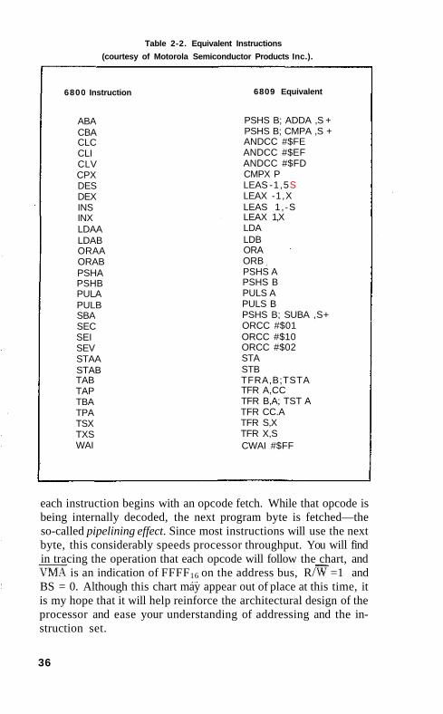
Table 2-2. Equivalent Instructions
(courtesy of Motorola Semiconductor Products Inc.).
6800 Instruction
ABA CBA CLC CLI CLV CPX DES DEX INS INX LDAA LDAB ORAA ORAB PSHA PSHB PULA PULB SBA SEC SEI SEV STAA STAB TAB TAP TBA TPA TSX TXS WAI
6809 Equivalent
PSHS B; ADDA ,S + PSHS B; CMPA ,S + ANDCC #$FE ANDCC #$EF ANDCC #$FD CMPX P LEAS -1,5S LEAX -1,X LEAS 1,-S LEAX 1,X LDA LDB ORA ORB PSHS A PSHS B PULS A PULS B PSHS B; SUBA ,S+ ORCC #$01 ORCC #$10 ORCC #$02 STA STB TFRA,B;TSTA TFR A,CC TFR B,A; TST A TFR CC.A TFR S,X TFR X,S CWAI #$FF
each instruction begins with an opcode fetch. While that opcode is being internally decoded, the next program byte is fetched—the so-called pipelining effect. Since most instructions will use the next byte, this considerably speeds processor throughput. You will find in tracing the operation that each opcode will follow the chart, and
is an indication of FFFF16 on the address bus, R/ =1 and BS = 0. Although this chart may appear out of place at this time, it is my hope that it will help reinforce the architectural design of the processor and ease your understanding of addressing and the instruction set.
36

Addressing Modes The first two chapters of this book were to get you into the swing of things and hopefully spark your interest in the 6809µ. This chapter is designed to build upon the power that I have hinted lies within the miniscule dot of silicon. Therefore, let's dig in.
You probably realize that the true power of any computer, regardless of size, is its ability to access memory. The addressing modes that the designers build in provide that capability. Within the 6809 µP, the addressing modes make it possible to extend the basic instruction set (59 instructions) to over 14 64. This statement in itself should tell you that a lot of power is possible.
BASIC CONCEPTS
This chapter is about addressing—what it is, how it works, and what modes and/or functions you have available with the 6809. In order to do this, however, it is necessary to lay down some ground rules to assist in the understanding of the subject. Consequently, rather than develop some odd-ball method. I have opted to use the same terms and definitions that Motorola prescribes.
Therefore, in the following descriptions the term effective address (EA) is used. The EA is the address in memory from which the argument for an instruction is fetched or stored. In two operand instructions, such as add to accumulator (ADD), one of the effective operands is used as a pointer. (The accumulator is inherent and not considered an addressing mode per se').
37

The following several pages provide descriptions and examples of the various modes of addressing the 6809 µP. To insure that understanding is achieved, I have provided examples for each mode and in some, but not all, cases the example is described in detail. Within these examples, you will see assembler instructions (described in Chapter 5) which should not be confused with an instruction set mnemonic. Specifically, I will be using the assembler instructions ORG, EQU and FCB. As does Motorola, I will use the parentheses in the examples to indicate "the contents of the location or resistor referred to. For example, (PC) indicates the contents of the location pointed to by the PC (Program Counter). The colon (:) is used to indicate a concatenation of bytes.
Furthermore, for convenience of description, it will be understood that the PC points one byte past the last byte of the instruction op code at the beginning of instruction execution. Other descriptive notation used throughout this book and Motorola and AMI documentation are shown in Tables 3-1, 3-2 and 3-3.
To fully appreciate this chapter, and to use it, I recommend that you look at the programmer's card located in Appendix C. This card will assist you in making the connection between the addressing mode and the instruction.
Before getting into the real meat of the matter, here is a run down of the types of addressing modes that will be discussed: inherent (includes accumulator), immediate, extended indirect, direct, register, indexed, zero-offset, constant offset, accumulator offset, auto increment/decrement, indexed indirect, relative, short/long relative branching and program counter relative addressing.
INHERENT ADDRESSING MODE This mode of addressing has no effective address (EA). The
opcode of the instruction contains all the address information
Table 3-1. Register Addressing Notation (courtesy of Motorola Semiconductor Products Inc.).
Accumulator Double Accumulator Index Register Stack Register Program Counter Direct Page Register Condition Code Register
ACCA or ACCB (A OR B) ACCA:ACCB or ACCD(D) IX or IY (X or Y) SP or US (S or U) PC (PC) DPR (DP) CCR (CC)
The Longer-form notation (i.e, ACCA, ACCB.ACCD, IX, IY,SP,US, PC, DPR, CCR) is used to describe the MPU resisters.The short-form notation (i.e.,A,B, D, X,Y, S, U, PC, DP, CC) is used by the 6809 assembler that is discussed later.
38

Accumulator Double-Accumulator Inherent
Table 3-2. Register Addressing Modes (courtesy of Motorola Semiconductor Products Inc.).
necessary. Inherent addressing instructions are the only type which do not include information in the operand field. Included in inherent addressing are : ABX, DAA, SWI, ASRA and CLRB.
Assembly Example 0500 5F CLRB 0501 3F SWI
In Table 3-4 accumulator B is cleared (filled with 00000000) and the processor in interrupted.
IMMEDIATE ADDRESSING
In immediate addressing, the EA of the data is the location immediately following the opcode. In other words, the data to be used in the instruction immediately follows the opcode of the instruction. The 6809 µP uses both 8 and 16-bit immediate values, depending on the size of argument specified by the opcode. Of course, immediate addressing implies that the data is a known value as the program is being created.
PC + 1 EA = PC PC + 1
PC
PC
Table 3-3. Memory Addressing Notations (courtesy of Motorola Semiconductor Products Inc.).
( ) = The (8-bit) data pointed to by the enclosed (16-bit) address. EA = The Effective Address; a pointer into memory created as a result of an addressing mode. M = (EA) = The data in the address space ('MEMORY') pointed to by the effective address. Ml = Memory Immediate Addressing; the data immediately following the last byte ot the OP code. dd = 8-bit. Offset, (or a relative distance to a label which evaluates to 8-bits). DDDD = 16-bit Offset (or a relative distance to a label). P = Immediate, Direct, Indexed, Extended. Q = Accumulator, Direct, indexed, Extended. YYYY = Offset such that - 64K <=YYYY <= 64K. ZZ = Any indexable register (IX, IY, SP, or US) XX = 8-bit hex value. * = PC at start of present instruction *' = Start of next instruction. IN = Indexed Addressing only # = Immediate Addressing Bytes(s) Follow(s). $ = Hex Value Follows. % = Binary Value Follows. < = Before indexing: force one-byte offset form (for known forward reference, or before
absolute address; force direct addressing (obtain warning If SETDP - M5 byte value > = Before absolute address; force extended addressing.
= Indexing symbol. = Indirection
39
[ ] ,
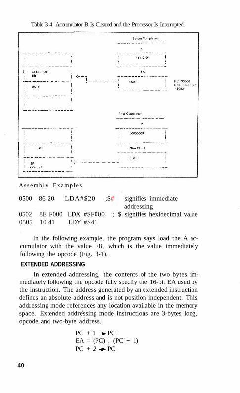
Table 3-4. Accumulator B Is Cleared and the Processor Is Interrupted.
A s s e m b l y E x a m p l e s
0500 86 20 LDA#$20 ;$# signifies immediate addressing
0502 8E F000 LDX #$F000 ; $ signifies hexidecimal value 0505 10 41 LDY #$41
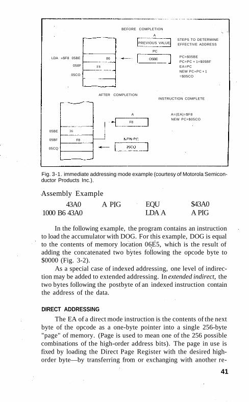
In the following example, the program says load the A accumulator with the value F8, which is the value immediately following the opcode (Fig. 3-1).
EXTENDED ADDRESSING
In extended addressing, the contents of the two bytes immediately following the opcode fully specify the 16-bit EA used by the instruction. The address generated by an extended instruction defines an absolute address and is not position independent. This addressing mode references any location available in the memory space. Extended addressing mode instructions are 3-bytes long, opcode and two-byte address.
PC + 1 PC EA = (PC) : (PC + 1) PC + 2 PC
40
BEFORE COMPLETION
PREVIOUS VALUE
AFTER COMPLETION
STEPS TO DETERMINE EFFECTIVE ADDRESS
PC=$05BE PC=PC + 1=$05BF EA=PC NEW PC=PC + 1 =$05CO
INSTRUCTION COMPLETE
A=(EA)=$F8 NEW PC=$05CO
Fig. 3-1. immediate addressing mode example (courtesy of Motorola Semiconductor Products Inc.).
Assembly Example
43A0 A PIG 1000 B6 43A0
EQU LDA A
$43A0 A PIG
In the following example, the program contains an instruction to load the accumulator with DOG. For this example, DOG is equal to the contents of memory location 06E5, which is the result of adding the concatenated two bytes following the opcode byte to $0000 (Fig. 3-2).
As a special case of indexed addressing, one level of indirection may be added to extended addressing. In extended indirect, the two bytes following the postbyte of an indexed instruction contain the address of the data.
DIRECT ADDRESSING
The EA of a direct mode instruction is the contents of the next byte of the opcode as a one-byte pointer into a single 256-byte "page" of memory. (Page is used to mean one of the 256 possible combinations of the high-order address bits). The page in use is fixed by loading the Direct Page Register with the desired high-order byte—by transferring from or exchanging with another re-
41
A
PC
LDA »$F8 05BE
058F
05CO
F8
05BE
05BF
05CQ
F8
36
F8
A
86 OSBE

gister. As a result, the EA consists of a high-order byte, from the DP register, catenated with a low-order byte from the instruction. The direct addressing mode for the 6809 µP is directly compatible to that of the 6800 µP.
EA = DPR: (PC)
Assembly Examples 0500 96 30 LDA $20 0502 10 SETDP $10 0505 D6 1030 LDB $1030
Several things are shown here. First, this mode requires less memory and executes faster than extended addressing. Of course, only 256 location (one page) can be accessed without redefining the contents of the DP register. Indirection is not allowed with this addressing mode. The next thing demonstrated is SETDP—Set Direct Page Pointer.
This directive is used by the assembler. It causes the assembler's 8-bit direct page pointer to be set to the value in the operand field—in this case a hex 10. This pointer is used when the assem-
LDA DOG 0409
040A
040B
040C
DOG FCB $40 06E5
LDA DOG 0409
040A
040B
040C
DOG FCB $40 06E5
Fig. 3-2. Extended addressing mode example (courtesy of Motorola Semiconductor Products Inc.).
BEFORE COMPLETION
PREVIOUS VALUE
AFTER COMPLETION
STEPS TO DETERMINE EFFECTIVE ADDRESS
PC=$0409 PC=PC + 1=$040A EA=(PC):(PC+1)
=$06E5 NEW PC = PC+2=$040C
INSTRUCTION COMPLETE
A=(EA)=$40
NEW PC=$040C
42
040C
NEW PC E5
B6
40
B6
06
0409
PC
$06E5
A
E5
06
A
40 40
EA 06E5

bler must decide whether to select the extended or direct mode of addressing. If the high or most significant (MS) byte of the EA is equal to the assembler's current direct page pointer, the direct mode is chosen. Otherwise, the extended mode is selected. The value in the operand field of the SETDP directive must be less than or equal to $FF.
In the following example of the Direct Addressing Mode the program contains an instruction to load the accumulator with CAT. For this example, CAT is equal to the contents of memory location 004B, which is the result of adding the byte following the opcode byte to $0000. Notice that this example is the same example that is used for explaining direct addressing for any of the 68XX family of processors, thus implying strict compatibility (Fig. 3-3).
REGISTER ADDRESSING
Register addressing implies no magic but merely references the selection of various on-board registers. Some of the opcodes are followed by a byte that defines a register or set of registers to be used by the instruction, which is called a postbyte (Table 3-5).
Examples
TFR X, Y Transfers X into Y EXG A, B Exchanges A with B PSHS A, B, X, Y Push onto S Y,X, B then A PULU X,Y, D Pull from U D,X, then Y
In the following assembly example, the REG—register directive—is used to define specific registers for specific labels. See Chapter 5. The registers are then pushed and pulled from the stack in the order that is characteristic of the 6809 µP. See Table 2-1. Assembly Example
0000 0002 0004
36 35 34
000F 0070 0070 70 70 0F
DOG CAT FROG PSHU PULS PSHS
REG REG REG #CAT #FROG #DOG
A,B,XX,DP S,X,Y U,X,Y
The interesting thing about this example, used courtesy of Motorola, is that a label assigned a value using the REG directive which contains the U register may not be used with the PSHU
43

CAT
CAT
FCB
LDA
FCB
LDA
$20
CAT
$20
CAT
004B
052D
052E
052F
004B
052D
052E
052F
BEFORE COMPLETION
20
D6
4B
A
PREVIOUS VALUE
PC
052D
EA 004B
AFTER COMPLETION
20
D6
4B
A
20
NEW PC
052F
STEPS TO DETERMINE EFFECTIVE ADDRESS
PC=$052D PC=PC+1=$052E EA=(PC)=$4B+$0000 =$004B NEW PC=PC +1 =$052F
INSTRUCTION COMPLETE A=(EA)=$20 NEW PC=$052F
Fig. 3-3. Direct addressing mode example (courtesy of Motorola Semiconductor Products Inc.).
instruction. Similarly, a value formed using the S register may not be used with PSHS instruction. The assembler will flag either of these forms with an error message.
INDEXED ADDRESSING
In all indexed addressing one of the pointer registers (X, Y, U, S and sometimes PC) is used in a calculation of the effective address (EA) of the operand to be used by the instruction. Five
Table 3-5. Push/Pull Postbyte (courtesy of American Microsystems, Inc.).
44
PC U Y X DP B A CC PSHS/PULS PULL ORDER PUSH ORDER
INCREASING MEMORY ADDRESS FFFF PC S Y X DP B A CC PSHU/PULU
0000
Push/Pull Postbyte

basic types of indexing are available and are included in this discussion. The postbyte of an indexed instruction specifies the basic type and variation of the addressing mode as well as the pointer register to be used. Table 3-6 lists the legal formats for the postbyte. Table 3-7 gives the assembler form and the number of cycles and bytes added to the basic values for indexed addressing for each variation. As a result of processor compatibility, most 6800 µP index mode instructions will map into an equivalent two bytes on the 6809 µP.
Zero-Offset Indexed
This option allows selection of auto increment/decrement by one or two bits; it is a minimum two-byte instruction (opcode + postbyte). When in this mode, the selected pointer register contains the EA of the data to be used by the instruction. This is the fastest indexing mode.
Examples LDD 0,X, LDA 0,S
Constant Offset Indexed
When this mode of addressing is used, a two's complement, offset and the contents of one of the pointer registers are added to form the effective address (EA) of the operand. The pointer register's initial content is unchanged by the addition. Three sizes of offset are available.
±4-bit (-16 to +15) ±7-bit (-128 to +127) ±15-bit (-32768 to +32767)
Constant offset, ±4 bits, use bit 4 of the postbyte as a sign bit and bits 0 through 3 as a constant offset. It is a minimum two-byte instruction.
Constant offset, ± 7 bits, designates the byte after the postbyte as a two's complement offset. It is a minimum three-byte instruction—opcode + postbyte + offset.
Constant offset, ± 15 bits, specifies the two bytes following the postbyte to be two's complement offset. It is a minimum four-byte instruction—opcode + postbyte + two-byte offset.
Other options are the two's complement 5-bit offset that is included in the postbyte and is most efficient in use of bytes and cycles. The two's complement 8-bit offset is contained in a single
45

Table 3-6. Indexed Addressing Postbyte Register
Bit Assignments (courtesy of American Microsystems, Inc.).
Bit Assignments
POST-BYTE REGISTER BIT
7
0
1
1
1
1
1
1
1
1
1
1
1
1
1
6
R
R
R
R
R
R
R
R
R
R
R
X
X
R
5
R
R
R
R
R
R
R
R
R
R
R
X
X
R
4
X
0
I
0
1
3
X
0
0
0
0
0
0
0
2
X
1
X
0
0
1
1
0
0
1
0
0
1
0
0
1
0
X
0
1
0
1
0
1
0
0
1
1
1
1
1
INDEXED ADDRESSING
MODE
EA = , R ± 4 BIT OFFSET
,R+
,R+ +
,-R
, - - R
EA = ,R + 0 OFFSET
EA = ,R±ACCB OFFSET
EA = ,R±ACCA OFFSET
EA = , B ± 7-BIT OFFSET
EA = ,R± 15-BIT OFFSET
EA = ,R±D OFFSET
EA = ,PC ± 7-BIT OFFSET
EA = ,PC ± 15-BIT OFFSET
EA = ,ADDRESS
ADDRESSING MODE FIELD
INDIRECT FIELD SIGN BIT WHEN B7 = 0
REGISTER FIELD 00:R = X 01:R = Y 10:R = U 11:R = S
X = DON'T CARE
byte following the postbyte, and the two's complement 16-bit offset is in the two-bytes following the postbyte. As a programmer you will normally not worry about the offset, since the assembler should take it into account.
Examples LDA 23,X LDX 2,S LDY 300,X
46

Example of constant-offset indexed indirect
LDA [, X] (note: the brackets indicate indirection) LDB [0,Y] LDX [64000,S]
Constant offset indexed indirect addressing functions in two stages like all indirects. First, the indexed address is formed by temporarily adding the offset-value contained in the addressing byte(s) to the value from the selected pointer register (X, Y,S,U, or PC). Then this address is used to recover a two-byte absolute pointer which is used as the EA.
The following example of the indexed addressing mode with a 16-bit offset contains an instruction to load the accumulator with a tabular value containing the hexadecimal number $DB (Fig. 3-4). This value is located in memory location 0780, which is the result of adding the concatenated two bytes following the opcode byte to the contents of the index register. Take out your programmer's calculator and add up the values to see what you get. From Fig. 3-4 you can see that this mode allows the programmer to use a "table of pointer" data structures, or to do I/O through absolute values stored on the stack.
Accumulator-Offset Indexed
When this option is chosen, it designates the A, B or D register as two's complement offset. The instruction is a minimum
Table 3-7. indexed Addressing Modes (courtesy of American Microsystems, Inc.}.
Type
Constant, Offset Frorm R
(Signed Offsets)
Accumulator Offset f r o m R
(Signed Offset)
Auto Increment/Decrement R
Constant Offset From PC
Extended indirect
Forms
No Otlset
5-Bit Offset
8 Bit Offset
16-Bit Offset
A — Register Offset
B — Register Offset
D — Register Offset
Increment By 1
Increment By 2
Decrement By 1
Decrement By 2
8-Bit Offset
16-Bit Offset
16 Bit Address
Non Indirect Indirect
Assembler
Form
R
n , R
n ,R
n ,R
A , R
B,R
D,R
R+
R + +
- R
- - R
n,PCR
n,PCR
-+ and -, indicate the number or additional cycles and bytes for the particular variation
Postbyte
Op Code
1RR00100
0RRnnnnn
1RR01000
1RR01001
1RR00110
1RR0010I
1RR01011
1RR00000
1RR00001
1RR00010
1RR00011
1XX01100
1XX01101
-
+ ~
0
1
1
4
1
1
4
2
3
2
3
1
5
-
+
#
0
0
1
2
0
0
0
0
0
0
0
1
2
-
Assembler
Form
[R]
Postbyte
OP Code
1RR10100
default to 8 bit
[n,R]
[n,R]
[A,R]
[B,R]
[D,R]
1RR11000
1RR11001
1RR10110
1RR10101
1RR11011
not allowed
[R++] 1RR10001
not allowed
[- -R]
[n ,PCR]
[n,PCR]
[n]
1RR10011
1XX11100
1XX11101
10011111
+ ~
3
4
7
4
4
7
6
6
4
8
5
+
#
0
1
2
0
0
0
0
0
1
2
2
R=X, Y. U or S X = 00 Y = 01
X = D o n ' t Care U = 10 S = 11
47
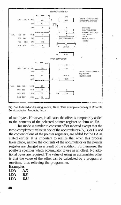
Fig. 3-4. Indexed addressing, mode, 16-bit offset example (courtesy of Motorola Semiconductor Products, Inc.).
of two-bytes. However, in all cases the offset is temporarily added to the contents of the selected pointer register to form an EA.
This mode is similar to constant offset indexed except that the two's complement value in one of the accumulators (A, B, or D), and the content of one of the pointer registers, are added for the EA as stated earlier. It is important to realize that when this process takes place, neither the contents of the accumulator or the pointer register are changed as a result of the addition. Furthermore, the postbyte specifies which accumulator to use as an offset. No additional bytes are required. The value of using an accumulator offset is that the value of the offset can be calculated by a program at run-time, thus relieving the programmer. Examples LDA A,X LDA B,Y LDA D,U
48
PC=$0692 PC=PC+1=$0693 EA=(PC):(PC+1)+(X) =$077E+$02 =$0780 NEW PC=PC+2 =$0695
ADDER
PREVIOUS VALUE
STEPS TO DETERMINE EFFECTIVE ADDRESS
PC
0692
077E
LDA TABL. X 0692
0693
0894
TABL FCB $BF 077E
FCB $86 007F
FCB $DB 0780
FCB $CF 0781
A6
07
7E
BEFORE COMPLETION
02
X
A BF
85
DB
CF
AFTER COMPLETION
X
02 A6 LDA TABL X 0592
0693
0694
0695
TABL FCB SGF 077E
FCB $86 007F
FCB $D8 0780
FCB $CF 0781 CF
08 DB
A 36
8F
0595
NEW PC 7E
07
0780 EA
INSTRUCTION COMPLETE A=(EA)=$DB NEW PC=$0695

Accumulator-indexed indirect addressing uses an accumulator (A,B or D) as a two's complement offset which is temporarily added to the value from the selected pointer register (X,Y,S, or U). The resulting pointer is then used to recover another pointer from memory —the indirect notation—which is then used as the EA. Auto Increment/Decrement Indexed
When the auto increment addressing mode is chosen, the pointer register contains the address of the operand. After the pointer register is used, it is incremented by one or two. This mode is extremely useful when you want to step through tables, move data or create software stacks. Conversely, the auto decrement mode suggests that the pointer register be decremented prior to its use as the pointer to the address of the data. This mode is very similar in operation to the increment mode, but everything is backwards. For example, tables would be scanned from the high to low addresses.
As indicated, the increment or decrement can be one or two to all for 8 or 16-bit tables. Of course, the step is programmer selectable. Because the decisions can be made before run-time, the programmer can establish additional software stacks that are identical to the U and S stacks. Examples
49
L D A ,X L D X , X + + L D A , Y + L D X , Y + + L D A , S + L D X , U + + L D A , U + L D X , S + +
Notice that the value in the selected pointer register addresses a one or two byte value in memory. No offset is permitted in this mode. Example
L D A [,X + + ] L D B [,Y + + ] L D D [ , S + + ] L D X [ ,U + + ]
This mode references auto-increment indirect. It uses the value in the selected pointer register (X,Y,S or U) to recover an address value from memory. This value is used as the EA. The register is then incremented by two ( + +)—incrementing by one in the indirect mode is illegal and no offset is permitted.

Example LDA ,-X LDX ,--X LDA ,-Y LDX ,--Y LDA ,-U LDX ,--U LDA ,-S LDX ,--S
In the auto-decrement addressing mode, the selected pointer register (X, Y,S or U) is decremented by one (-) or two (--) and is user selectable. The resulting value then becomes the EA. Example LDA [ , - -X] LDB [ , - -Y] LDD [ , - -U] LDX [,--S]
Auto-decrement indirect first decrements the selected pointer register by two (--). An auto-decrement of one is prohibited. The resulting value is used to recover a pointer value from memory and is the EA.
INDEXED INDIRECT With the exception of the ± 4-bit constant offset and the
auto-increment/decrement by one, all indexed addressing modes may be used with an additional level of indirection. The address formed by adding the offset to the selected pointer register designates a location containing the EA of the operand data. Bit 4 of the postbyte is used to select the indexed indirect mode. Interestingly enough, this same bit (bit 4) is used as a sign bit in the ± 4-bit constant offset mode. Regardless of indexing mode direct or indirect, the same number of bytes are used.
In this indirect mode, the EA is contained at the location specified by the content of the index register plus any offset. In the following example, the A accumulator is loaded indirectly using an EA calculated from the index register and an offset. It is reprinted courtesy of Motorola. Example
Before execution A AA = XX (don't care)
X =$F000
$0100 LDA 10.X EA is now$F010 $F010 $F1 F150 is now the new EA $F011 $50Q $F150 $AA After Execution
A AA=$AA Actual Data Loaded
50
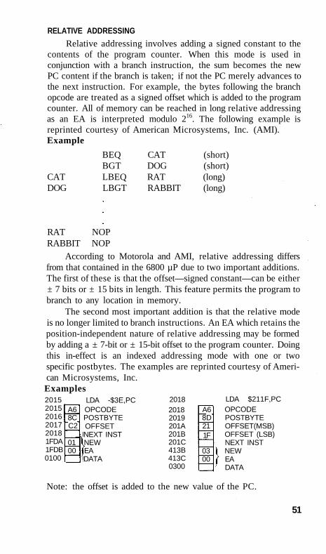
RELATIVE ADDRESSING
Relative addressing involves adding a signed constant to the contents of the program counter. When this mode is used in conjunction with a branch instruction, the sum becomes the new PC content if the branch is taken; if not the PC merely advances to the next instruction. For example, the bytes following the branch opcode are treated as a signed offset which is added to the program counter. All of memory can be reached in long relative addressing as an EA is interpreted modulo 216. The following example is reprinted courtesy of American Microsystems, Inc. (AMI). Example
Note: the offset is added to the new value of the PC.
51
BEQ CAT (short) BGT DOG (short)
CAT LBEQ RAT (long) DOG LBGT RABBIT (long)
RAT NOP RABBIT NOP
According to Motorola and AMI, relative addressing differs from that contained in the 6800 µP due to two important additions. The first of these is that the offset—signed constant—can be either ± 7 bits or ± 15 bits in length. This feature permits the program to branch to any location in memory.
The second most important addition is that the relative mode is no longer limited to branch instructions. An EA which retains the position-independent nature of relative addressing may be formed by adding a ± 7-bit or ± 15-bit offset to the program counter. Doing this in-effect is an indexed addressing mode with one or two specific postbytes. The examples are reprinted courtesy of American Microsystems, Inc. Examples
LDA $211F,PC OPCODE POSTBYTE OFFSET(MSB) OFFSET (LSB) NEXT INST NEW EA DATA
LDA -$3E,PC OPCODE POSTBYTE OFFSET NEXT INST NEW EA DATA
2015 2015 2016 2017 2018 1FDA 1FDB 0100
A6 8C C2
01 00
2018 2018 2019 201A 201B 201C 413B 413C 0300
A6 8D 21 1F
03 00

Table 3-8. 8-Bit Accumulator and Memory Instructions (courtesy of American Microsystems, Inc.).
8-Bit Accumulator and Memory Instructions
Mnemonic(s)
ADCA, ADCB
ADDA, ADDB
ANDA, ANDB
ASL
ASLA, ASLB
ASR
ASRA, ASRB
BITA, BITB
CLR
CLRA, CLRB
CMPA, CMPB
COM
COMA, COMB
DAA
DEC
DECA. DECB
EORA. EORB
EXG R1, R2
INC
INCA, INCB
LDA, LDB
LSL
LSLA, LSLB
LSR
LSRA, LSRB
MUL
NEG
NEGA. NEGB
ORA, ORB
ROL
ROLA, ROLB
ROR
RORA, RORB
SBCA, SBCB
STA, STB
SUBA, SUBB
TST
TSTA, TSTB
TFR,R1, R2
Operation
Add memory to accumulator with carry
Add memory to accumulator
And memory with accumulator
Arithmetic shift left memory location
Arithmetic shift left accumulator
Arithmetic shift right memory location
Arithmetic shift right accumulator
Bit test memory with accumulator
Clear memory location
Clear accumulator
Compare memory with accumulator
Complement memory location
Complement accumulator
Decimal adjust A-accumulator
Decrement memory location
Decrement accumulator
Exclusive or memory with accumulator
Exchange R1 with Rs (R1. R2 = A, B, CC, DP)
Increment memory location
Increment accumulator
Load accumulator from memory
Logical shift left memory location
Logical shift left accumulator
Logical shift right memory location
Logical shift right accumulator
Unsigned multiply (AXB=D)
Negate memory location
Negate Accumulator
Or memory with accumulator
Rotate memory location left
Rotate accumulator left
Rotate memory location right
Rotate accumulator right
Subtract memory from accumulator with borrow
Store accumulator to memory
Subtract memory from accumulator
Test memory location
Test accumulator
Transfer R1 to R2 (R1, R2 = A. B. CC. DP)
Addressing Modes
Imp
lied
— — — — X — X — — X — — X X
— X — X — X — X X — X X
— X — — X — X — — — — X X
Imm
edia
te
X X X —
— —
— X —
— X —
— —
— — X
— —
— X —
— —
— — —
— X —
— —
— X
— X — — —
X X X X — X — X X
— X X — — X — X — X — X X — X — — X — X X — X — X X X X — —
Ext
end
ed
X X X X
— X
— X X
— X X
— —
X — X
— X
— X X
— X
— — X
— X X
— X
— X X X X — —
Ext
end
ed I
nd
irec
t
X X X X — X
— X X — X X — — X — X — X — X X — X — — X — X X — X — X X X X — —
Ind
exed
X X X X
— X
— X X
— X X
— —
X — X
— X
— X X
— X
— —
X —
X X
— X
— X X X X —
—
Ind
exed
In
dir
ect
X X X X — X — X X — x X — — X — X — X — X X — X — — X — X X — X — X X X X — —
Rel
ativ
e
X X X X
— X
— X X
— X X
— —
X — X
— X
— X X
— X
— —
X —
X x
— X
— X X X X — —
Rel
ativ
e In
dir
ect
X X X X
— X
— X X
— X X
— —
X — X
— X
— X X
— X
— —
X —
X X
— X
— X X X X — —
NOTE: A and 8 may be pushed to (pulled from) either stack with PSHs. PSHU (PULS. PULU) instructions.
Relative Indirect This mode in actual use is indexed with the PC being used as
the index register or in concert with the prime register. One or two bytes past the postbyte are used to provide a ± 7 bit or ± 15 bit offset. The resulting signed number is then added to the contents of the PC, which then forms a pointer to consecutive locations in memory that contain the new EA. This example is courtesy of American Microsystems, Inc.
52

Table 3-9. 16-Bit Accumulator and Memory
Instructions (courtesy of American Microsystems, Inc.).
16-Bit Accumulator and Memory Instructions
Mnomonic(s) Operation
ADDD Add memory to D accumulator CMPD Compare memory with D accumulator
EXG D,R Exchange D with X, Y S. U, or PC
LDD Load D accumulator from memory SEX Sign Extend
STD Store D accumulator to memory SUBD Subtract memory from D accumulator
TFR D,R Transfer D to X. Y, S, U. or PC
TFR R,D Transfer X. Y. S, U, or PC to D
Addressing Modes
Impl
ied
— — X — X — — X X
Imm
edia
te
X X — X — — X — —
Dire
ct
X X
— X
— X X
— —
Ext
ende
d
X X
— X — X x
— —
Ext
ende
d In
dire
ct
X X — X — X X — —
Inde
xed
X X
— X
— X X
— —
X X — X — X X — —
Rel
ativ
e
X X — X
— X X — —
Rel
ativ
e In
dire
ct
X X
— X
— X X
— —
Example
2015 LDA -$3E,PC 2015 A6 OPCODE 2016 9C POSTBYTE 2017 C2 OFFSET 2018 NEXT INST
1FDA
1FDB
0100
01
00
NEW
EA
DATA
2018 2018 2019 201A 201B
201C
413B
413C
LDA A6 9D 21 1F
03
00
$2115,PC OPCODE POSTBYTE OFFSET (MSB) OFFSET (LSB)
NEXT INST
NEW
EA
0300 DATA
Table 3-10. Index Register/Stack Pointer Instructions (courtesy of American Microsystems, Inc.).
Mnemonic(s)
CMPS. CMPU CMPX. CMPY
EXG R1. R2
LEAS, LEAU LEAX. LEAY
LDS, LDU LDX, LDV
PSHS
PSHU PULS PULU
STS, STU STX, STY
TFR R1,R2
ABX
index Register/Stack Pointer Instructions
Operation Compare memory with stack pointer
Compare memory with index register
Exchange D, X, Y, S, U, or PC with D, X, Y, S, U, or PC Load eftectfve address into stack pointer Load effective address into index register
Load slack pointer from memory Load index register trom memory Push any register(s) onto hardware stack (except S)
Push any register(s) onto user stack (except U)
Pull any register(s) trom hardware stack (except S) Pull any register(s) from hardware stack (except U) Store stack pointer to memory
Store index register to memory
Transfer D, X, U. or PC to 0, X, S, U, or PC
Add B-accumulator to X (unsigned)
Addressing Modes
impl
ied
— —
X
— — — — X X X X — — X X
Imm
edia
te
X X
—
— — X X — — — — — — — —
Dire
ct
X X
—
— — X X
—
— —
— X X — —
Exte
nded
X X
—
— — X X — — — — X X — —
Exte
nded
indi
rect
X X —
X X X X — — — — X X — —
Inde
xed
X X
—
X X X X
— — — —
X X
— —
Inde
xed
indi
rect
X X
—
X X
X X — — — — X X —
—
Rel
ativ
e
X X
—
X
X X X — — — — X X — —
Rel
ativ
e In
dire
ct
X X
—
X X X X
— —
— — X X
— —
53

Table 3-11. Branch Instructions (courtesy of American Microsystems, Inc.).
Branch Instructions
Mnemonic(s) Operation
BCC. LBCC Branch if carry clear BCS. LBCS Branch if carry set BEQ. LBEQ Branch if equal
BGE. LBGE Branch if greater than or equal (signed) BGT. LBGT Branch if greater (signed) BHI. LBHI Branch if higher (unsigned)
BHS. LBHS Branch if higher or same (unsigned)
BLE. LBLE Branch if less than or equal (signed) BLO. LBLO Branch if lower (unsigned)
BLS. LBLS Branch if lower or same (unsigned] BLT. LBLT Branch if less than (signed) BMI. LBMI Branch if minus
BNE. LBNE Branch if not equal BPL. LBPL Branch if plus BRA. LBRA Branch always
BRN. LBRN Branch never (3.5 Cycle NOP)
BSR. LBSR Branch to subroutine BVC. LBVC Branch if overflow clear
BVS. LBVS Branch if overllow set
Addressing Modes
Imm
edia
te
Dire
ct
Exte
nded
Exte
nded
Indi
rect
Inde
xed
Inde
xed
Indi
rect
Rel
ativ
e
X X
X X X
X X
X X X
X
X X
X X
X X X
X
Rel
ativ
e In
dire
ct
Extended Indirect
This is another option of indexed indirect addressing. For the extended mode, two bytes following the postbyte are used as a pointer to consecutive locations in memory which contain the new effective address. The example is courtesy of American Microsystems, Inc. Example
201C 201C 201D 201E 201F 2020
C200 C201 0080
LDA A6 9F C2 00
00 80
C200 OPCODE POSTBYTE
POINTER
NEXT INST
NEW EA DATA
Absolute Indirect
The processor must have some method of restarting and handling interrupt vectors. This addressing mode is exclusively for that purpose and no other. The conditions are serviced by fetching the contents of exact memory locations and loading it into the PC. Nothing more and nothing less happens.
54

Table 3-12. Miscellaneous Instructions (courtesy of American Microsystems, Inc.).
Mnemonic(s)
ANDCC CWA NOP
ORCC
JMP
JSR RTI
RTS
SYNC
Miscellaneous Instructions
Operation
AND condition code register AND condition code register, Then wait for interrupt No operation OR condition code register
Jump
Jump to subroutine Return trom interrupt
Return from subroutine
Software interrupt (absolute indirect)
Synchronize with interrupt line
Addressing Modes
Impl
ied
X
X
X
X
X
X X
X X X
Exte
nded
X X
Exte
nded
Indi
rect
X X
Inde
xed
X X
Inde
xed
Indi
rect
X X
X X
Rel
ativ
e In
dire
ct
X X
SUMMARY
This chapter is a tough one to understand. I'm reasonably sure that on this first reading you haven't grasped everything that was presented. You will quite naturally have to reread this chapter and actually try the concepts explained before they really mean anything to you. However, as a quick reference I've included Tables 3-8 through 3-12 to help put the various instructions in perspective as far as addressing goes and get you ready for the next chapter on the instruction set.
55

Into the Instruction Set Now that you have an understanding of how the 6809 µP works and the various methods of addressing, the next step is to become familiar with the instruction set. As discussed in Chapter 1, the 6809 is similar to that of the 6800 µP, and in most cases has the same instructions except where noted in Chapter 2. The 6809 µP as designed is upward compatible at the source level. This means that you can use 6800 instructions in a 6809 assembly and end up with a working program, which you will see in Chapter 6.
One difference that is readily discernible is the number of opcodes has been reduced from 72 to 59, primarily because of the expanded architecture and additional addressing modes. See Chapter 3. Because of the additional addressing modes, the number of available opcodes has risen from 197 to 1464—a considerable jump and indication of the type of programming power you have available to you. Before getting into a breakdown of the instruction codes, a brief overview is due to give you a better idea of what is in store.
PUSH PULL AND ADDRESS IT
Some things you might not be aware of are the use of push (PSH) and pull (PUL), the transferring of register contents (TFR) and (EXG), the method of loading the EA (LEA), multiplying accumulators (MUL), and long and short relative branches. These and other functions of the 6809 µP are important concerns for the programmer to become familiar with and are covered here to assist in understanding.
56

P S H U / P S H S
The push instructions have the capability of pushing onto either hardware stack (S) or user stack (U). Any or all of the MPU register with a single instruction. In Chapter 3 I showed you how a register set could be predefined to permit pushing several defined registers on the stack at one time.
P U L U / P U L S
The pull instructions have the same capability of the push instruction in reverse order. The byte immediately following the push or pull opcode determines which register or registers are to be pushed or pulled. The actual PUSH/PULL sequence is fixed; each bit defines a unique register to push or pull. This push/pull postbyte was demonstrated in Table 3-5.
TFR/EXG
One of the powerful features of the 6809 µP is that any register of like size may be transferred content wise with the other, or the contents exchanged. For example, an 8-bit register can be transferred or exchanged with another 8-bit register and so on. When this feature is used, the bits 4-7 of the postbyte define the source register while bits 0-3 represent the destination. The following combinations are the valid definitions for these register transfers.
0000 - D 0001 - X 0010 - Y 0011 - U 0100 - S
0101 - PC 1000 - A 1001 - B 1010 - CC 1011 - DP
Load Effective Address (LEA)
One of the methods used by the 6809 µP to speed up processing is to use this instruction. What happens is that the LEA calculates the EA used in an indexed instruction and stores that address value, rather than the data at that address, in a pointer register. This functional addressing makes all the features of the internal addressing hardware available to the programmer, and suggests that the 6809 is a 16-bit processor in reality. Table 4-1 is an example of LEA and demonstrates its power.
Multiply (MUL)
This is a powerful instruction that multiplies unsigned binary numbers in the A and B accumulator and then places the result into
57

Table 4-1.LEA Examples (courtesy of American Microsystems, Inc.),
Comment
! Adds 5-bit constant 10 to X ! Adds 6-bit constant 500 to X ! Adds 8-bit accumulator to Y ! Subtracts 10 from 11 ! Used to reserve area on stack ! Used to clean up stack ! Transfers as well as adds.
Long and Snort Relative Branches I would imagine that the first thing that comes to mind is that
this is really something difficult to master. Actually, the 6809 has the capability of PC relative branching throughout the entire memory map. When in this mode and a branch is to be taken, the 8 or 16-bit offset value is added to the PC to make the EA. Consequently, this permits the processor to branch anywhere within a 64K memory map. Position independent code can be easily generated by using relative branching. Incidentally, short refers to 8-bit and long to 16-bit.
This is a unique instruction since it stops the MPU and makes it wait for an interrupt. If the pending interrupt is nonmaskable (NMI) or maskable (FIRQ, IRQ) with its mask bit (F or I) clear, the processor will clear the Sync state and perform the normal interrupt stacking and servicing routine. You can see that this makes it possible to handle specialized interrupts and develop programs that work well in process control or data acquisition.
Instruction Operation
LEAX LEAX LEAY LEAY LEAS LEAS LEAX
10,X 500,X
A,Y -10,U -10,S
10,S 5,S
X+10 X+500 Y+A U-10 S-10 S+10 S+5
- > X - > X - > Y ->U ->S - > S - > X
the 16-bit D accumulator. This permits multiple-precision multiplications.
Software Interrupts (SWB) If you are familiar with the 6800 µP, then you have some ideas
what a software interrupt is for. It is the instruction that will cause an interrupt in the course of program execution and will permit a goto for the associated vector fetch. Three levels of SWI are available on the 6809 and have a priority status of SWI, SWI2 and SWI3.
58
SYNC

These operations make the 6809 a high-powered µP and excellent precursor to 16-bit processors. The 6809 can process 16-bit datas on an 8-bit structure with almost the same power as its big brother the 68000. Included in these 16-bit instructions are: loads, stores, compares, adds, subtracts, transfers, exchanges, pushes and pulls. Refer again to Tables 3-8 through 3-12 which are summaries of the instruction set. Associated with this chapter is Appendix B which covers the hexadecimal values of machine codes, coupled with Appendix C, the programmer's quick reference card.
The next several pages will cover each instruction available on the 6809 µP. You will notice that in concert with the instruction mnemonic, I have provided the various addressing modes and the associated opcode. This sequence of presentation is coupled with the Instruction Index, located in Appendix D. The purpose is to assist you in finding the proper instruction for a particular purpose. I would suggest that as you proceed through this section of the chapter you look at the programmer's card, found in Appendix C, and use it to follow along. This will help you become familiar with each instruction and the card.
See Tables 4-2 and 4-3 for the notation that is used in the explanation of the instruction set. The notation is used by Motorola and consequently provides continuity in explanation.
ABX ADD ACCB INTO IX
SOURCE FORM: ABX
OPERATION: IX'
CONDITION CODES: NOT AFFECTED
DESCRIPTION: Add the 8-bit unsigned value in Accumulator B into the X index register.
ADDRESSING MODE:
INHERENT
OPCODE
3A
MPU CYCLES
3
NO OF BYTES
1
59
INDIVIDUAL INSTRUCTIONS
IX + ACCB
18-Bit Operations
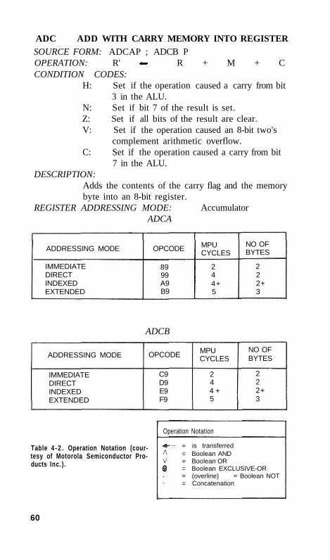
ADC ADD WITH CARRY MEMORY INTO REGISTER SOURCE FORM: ADCAP ; ADCB P OPERATION: R' R + M + C CONDITION CODES:
H: Set if the operation caused a carry from bit 3 in the ALU.
N: Set if bit 7 of the result is set. Z: Set if all bits of the result are clear. V: Set if the operation caused an 8-bit two's
complement arithmetic overflow. C: Set if the operation caused a carry from bit
7 in the ALU. DESCRIPTION:
Adds the contents of the carry flag and the memory byte into an 8-bit register.
REGISTER ADDRESSING MODE: Accumulator ADCA
ADDRESSING MODE
IMMEDIATE DIRECT INDEXED EXTENDED
OPCODE
89 99 A9 B9
MPU CYCLES
2 4 4+ 5
NO OF BYTES
2 2 2+ 3
ADCB
ADDRESSING MODE
IMMEDIATE DIRECT INDEXED EXTENDED
OPCODE
C9 D9 E9 F9
MPU CYCLES
2 4 4 + 5
NO OF BYTES
2 2 2+ 3
Table 4 - 2 . Operation Notation (courtesy of Motorola Semiconductor Products Inc.) .
Operation Notation
= is transferred = Boolean AND = Boolean OR = Boolean EXCLUSIVE-OR = (overline) = Boolean NOT = Concatenation
60

ADD ADD MEMORY INTO REGISTER - 8-BIT SOURCE FORMS: ADDA P; ADDB P OPERATION: R' R + M CONDITION CODES:
H: Set if the operation caused a carry from bit 3 in the ALU.
N: Set if bit 7 of the result is set Z: Set if all bits of the result are clear. V: Set if the operation caused an 8-bit two's
complement arithmetic overflow. C: Set if the operation caused a carry from bit
7 in the ALU. DESCRIPTION:
Adds the memory byte into an 8-bit register. REGISTER ADDRESSING MODE: Accumulator
ADDA
ADDRESSING MODE
IMMEDIATE DIRECT INDEXED EXTENDED
OPCODE
8B 9B AB BB
MPU CYCLES
2 4 4+ 5
NO OF BYTES
2 2 2+ 3
ADDB
ADDRESSING MODE
IMMEDIATE DIRECT INDEXED EXTENDED
OPCODE
CB DB EB FB
MPU CYCLES
2 4 4+ 5
NO OF BYTES
2 2 2+ 3
ADDD
ADDRESSING MODE
IMMEDIATE DIRECT INDEXED EXTENDED
OPCODE
C3 D3 E3 F3
MPU CYCLES
4 6 6+ 7
NO OF BYTES
3 2 2+ 3
This instruction ADDD is the 16-bit version. For this the 16-bit version. For this the operation is R' R + M:M+1. The condition codes are: H: not affected; N: Set if bit 15 of the result
61
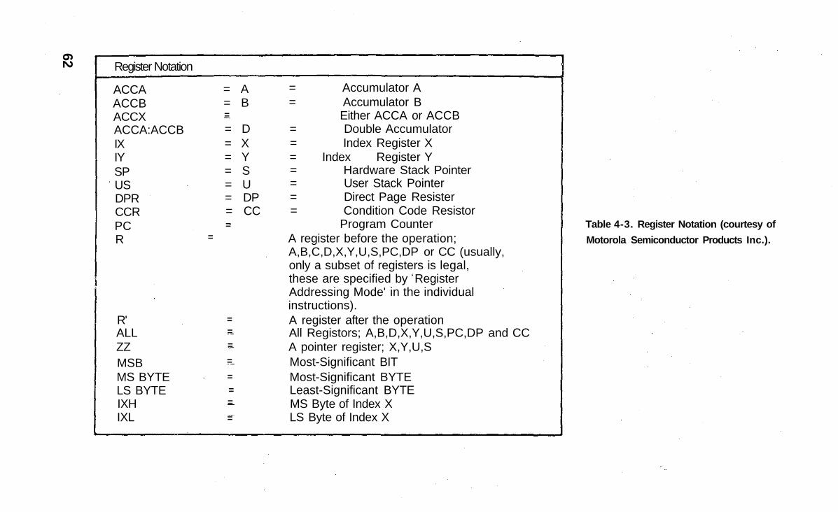
Register Notation
ACCA ACCB ACCX ACCA:ACCB IX IY SP US DPR CCR PC R
R' ALL ZZ MSB MS BYTE LS BYTE IXH IXL
= A = B =
= D = X = Y = S = U = DP = CC =
=
= = =
=
= = =
=
= Accumulator A = Accumulator B
Either ACCA or ACCB = Double Accumulator = Index Register X = Index Register Y = Hardware Stack Pointer = User Stack Pointer = Direct Page Resister = Condition Code Resistor
Program Counter A register before the operation; A,B,C,D,X,Y,U,S,PC,DP or CC (usually, only a subset of registers is legal, these are specified by Register Addressing Mode' in the individual instructions). A register after the operation All Registors; A,B,D,X,Y,U,S,PC,DP and CC A pointer register; X,Y,U,S Most-Significant BIT Most-Significant BYTE Least-Significant BYTE MS Byte of Index X LS Byte of Index X
Table 4-3. Register Notation (courtesy of
Motorola Semiconductor Products Inc.).
62

is set; Z: Set if all bits of the result are clear; V: Set if there was a 16-bit two's complement arithmetic overflow; and C: set if the operation on the MS byte caused a carry from bit 7 in the ALU. This instruction adds the 16-bit memory value into the 16-bit accumulator (D) and has a register addressing mode of double accumulator. The memory addressing modes are shown above.
In the next group of instructions, the logical AND is implied. The logical AND is best explained by assuming that it has the property such that if X and Y are two logic variables, then the function X AND Y is defined by the following:
X Y X AND Y X Y X AND Y 0 0 0 1 0 0 0 1 0 1 1 1
A basic operation in Boolean algebra is the AND operation which, for the two integers I and J, may be defined by saying if I and J are both 1, then the result is 1. If I is 0 and J is 1, then the result is 0 and vice versa.
AND LOGICAL AND MEMORY INTO REGISTER
SOURCE FORMS: ANDA P; ANDB P OPERATION: R' R AND M CONDITION CODES:
H-. Not Affected N: Set if bit 7 of result is set Z: Set if all bits of result are clear V: Cleared C: Not affected
DESCRIPTION: Performs the logical "AND" operation between the contents of ACCX and the contents of M and the result is stored in ACCX.
REGISTER ADDRESSING MODE: Accumulator
ANDA
ADDRESSING MODE
IMMEDIATE DIRECT INDEXED EXTENDED
OPCODE
84 94 A4 B4
MPU CYCLES
2 4 4+ 5
NO OF BYYTES
2 2 2+ 3
83

ANDB
ADDRESSING MODE
IMMEDIATE DIRECT INDEXED EXTENDED
OPCODE
C4 D4 E4 F4
MPU CYCLES
2 4 4+ 5
NO OF BYTES
2 2 2+ 3
AND LOGICAL AND IMMEDIATE MEMORY INTO CCR
SOURCE FORM: ANDCC #XX OPERATION: R' R AND MI CONDITION CODES'. CCR' CCR MI DESCRIPTION:
Performs a logical "AND" between the CCR and the MI byte and places the result in the CCR.
ANDCC
ADDRESSING MODE
MEMORY IMMEDIATE
OPCODE
1C
MPU CYCLES
3
NO OF BYTES
2
ASL ARITHMETIC SHIFT LEFT SOURCE FORM: ASL Q OPERATION:
CONDITION CODES: H: Undefined N: Set if bit 7 of the result is set Z: Set if all bits of the result are clear V: Loaded with the result of (b7 b8) of
the original operand. C: Loaded with bit 7 of the original operand.
DESCRIPTION: Shifts all bits of the operand one place to the left. Bit 0 is loaded with a zero. Bit 7 of the operand is shifted into the carry flag.
64

ASIA
ADDRESSING MODE
ACCUMULATOR
OPCODE
48
MPU CYCLES
2
NO OF BYTES
1
ASLB
ADDRESSING MODE
ACCUMULATOR
OPCODE
58
MPU CYCLES
2
NO OF BYTES
1
ASL
ADDRESSING MODE
DIRECT EXTENDED INDEXED
OPCODE
08 78 68
MPU CYCLES
6 7 6+
NO OF BYTES
2 3 2+
ASR ARITHMETIC SHIFT RIGHT
SOURCE FORM: ASR Q
OPERATION:
CONDITION CODES: H: Undefined N: Set if bit 7 of the result is set Z: Set if all bits of result are clear V: Not affected C: Loaded with bit 0 of the original operand
DESCRIPTION: Shifts all bits of the operand right one place. Bit 7 is held constant. Bit 0 is shifted into the carry flag. The 6800/01/02/03/08 processors do affect the V flag.
65

ASR
ADDRESSING MODE
INHERENT DIRECT EXTENDED INDEXED
OPCODE
57 07 77 67
MPU CYCLES
2 6 7 6 +
NO OF BYTES
1 2 3 2+
ASRA
ADDRESSING MODE
INHERENT
OPCODE
47
MPU CYCLES
2
NO OF BYTES
1
BCC BRANCH ON CARRY CLEAR
SOURCE FORM: BCC dd; LBCC DDDD OPERATION: TEMP MI
if C = 0 THEN PC' PC + TEMP CONDITION CODES:
Not affected DESCRIPTION:
Tests the state of the C bit and causes a branch if C is clear.
MEMOR Y ADDRESSING MODE: Memory Immediate COMMENTS:
When used after a subtract or compare on unsigned binary values, this instruction could be called "branch" if the resister was higher or the same as the memory operand.
BCC
ADDRESSING MODE
RELATIVE
OPCODE
24
MPU CYCLES
3
NO OF BYTES
2
LBCC
ADDRESSING MODE
RELATIVE
LONG BRANCH
OPCODE
10
MPU CYCLES
5(6)
NO OF BYTES
4
BCS
OPERATION: TEMP
BRANCH ON CARRY SET
MI
if C = 1 THEN PC' PC + TEMP
66
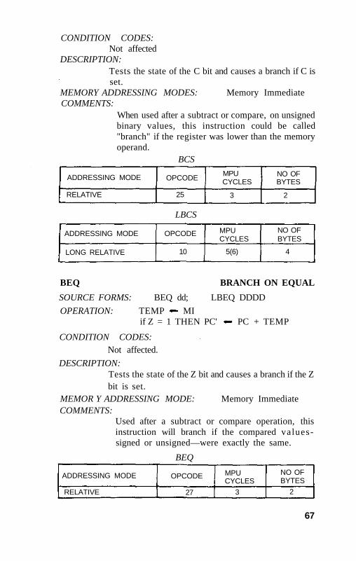
CONDITION CODES: Not affected
DESCRIPTION: Tests the state of the C bit and causes a branch if C is set.
MEMORY ADDRESSING MODES: Memory Immediate COMMENTS:
When used after a subtract or compare, on unsigned binary values, this instruction could be called "branch" if the register was lower than the memory operand.
BCS
ADDRESSING MODE
RELATIVE
OPCODE
25
MPU CYCLES
3
NO OF BYTES
2
LBCS
ADDRESSING MODE
LONG RELATIVE
OPCODE
10
MPU CYCLES
5(6)
NO OF BYTES
4
BEQ BRANCH ON EQUAL
SOURCE FORMS: BEQ dd; LBEQ DDDD
OPERATION: TEMP MI if Z = 1 THEN PC' PC + TEMP
CONDITION CODES: Not affected.
DESCRIPTION: Tests the state of the Z bit and causes a branch if the Z bit is set.
MEMOR Y ADDRESSING MODE: Memory Immediate COMMENTS:
Used after a subtract or compare operation, this instruction will branch if the compared values-signed or unsigned—were exactly the same.
BEQ
ADDRESSING MODE
RELATIVE
OPCODE
27
MPU CYCLES
3
NO OF BYTES
2
67

LBEQ
ADDRESSING MODE
LONG RELATIVE
OPCODE
10
MPU CYCLES 5(6)
NO OF BYTES
4
BGE BRANCH ON GREATER THAN OR EQUAL TO ZERO
SOURCE FORMS: BGE dd; LBGE DDDD OPERATION: TEMP MI
if [N V] = 0 THEN PC' PC + TEMP CONDITION CODES:
Not affected DESCRIPTION:
Causes a branch if N and V are either both set or both clear. For example, branch if the sign of a valid two's complement result is, or would be, positive.
MEMOR Y ADDRESSING MODE: Memory Immediate COMMENTS:
Used after a subtract or compare operation on two's complement values, this instruction will branch if the register was greater than or equal to the memory operand.
BGE
ADDRESSING MODE
RELATIVE
OPCODE
2C
MPU CYCLES
3
NO OF BYTES
2
LBGE
ADDRESSING MODE
LONG RELATIVE
OPCODE
10
MPU CYCLES
5(6)
NO OF BYTES
4
BGT Branch on Greater SOURCE FORMS: BGT dd; LBGT DDDD OPERATION: TEMP MI
if Z V[N V] = 0 then PC' PC + TEMP CONDITION CODES: Not affected DESCRIPTION:
Causes a branch if (N and V are either both set or both clear) and Z is clear. In other words, branch if the sign of a valid two's complement result is, or would be, positive and non-zero.
68
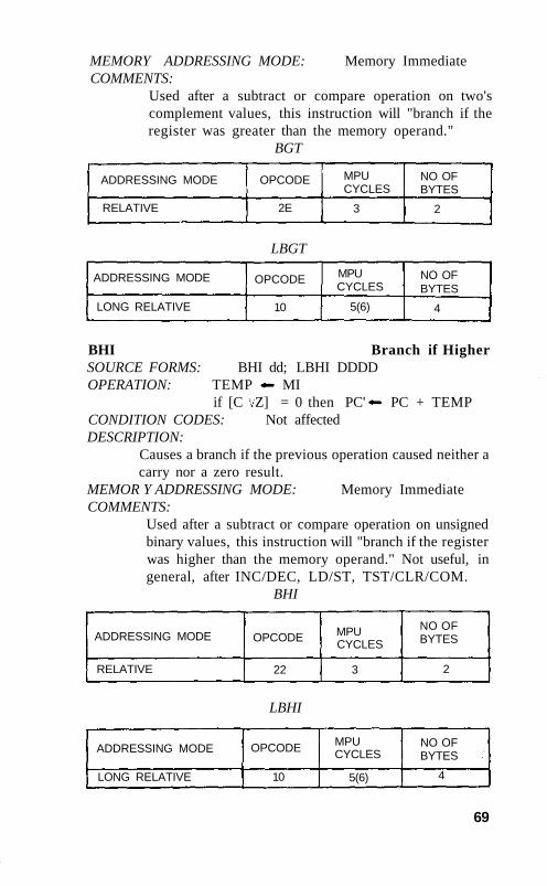
MEMORY ADDRESSING MODE: Memory Immediate COMMENTS:
Used after a subtract or compare operation on two's complement values, this instruction will "branch if the register was greater than the memory operand."
BGT
ADDRESSING MODE
RELATIVE
OPCODE
2E
MPU CYCLES
3
NO OF BYTES
2
LBGT
ADDRESSING MODE
LONG RELATIVE
OPCODE
10
MPU CYCLES
5(6)
NO OF BYTES
4
BHI Branch if Higher SOURCE FORMS: BHI dd; LBHI DDDD OPERATION: TEMP MI
if [C Z] = 0 then PC' PC + TEMP CONDITION CODES: Not affected DESCRIPTION:
Causes a branch if the previous operation caused neither a carry nor a zero result.
MEMOR Y ADDRESSING MODE: Memory Immediate COMMENTS:
Used after a subtract or compare operation on unsigned binary values, this instruction will "branch if the register was higher than the memory operand." Not useful, in general, after INC/DEC, LD/ST, TST/CLR/COM.
BHI
ADDRESSING MODE
RELATIVE
OPCODE
22
MPU CYCLES
3
NO OF BYTES
2
LBHI
ADDRESSING MODE
LONG RELATIVE
OPCODE
10
MPU CYCLES
5(6)
NO OF BYTES
4
69

BHS Branch if Higher or Same SOURCE FORM: BUS dd; LBHS DDDD OPERATION: TEMP MI
if C = 0 then PC PC' PC + 1 MI CONDITION CODES: Not Affected DESCRIPTION:
Tests the state of the C-bit and causes a branch if C is clear.
MEMORY ADDRESSING MODE: Memory Immediate COMMENTS:
When used after a subtract or compare on unsigned binary values, this instruction will "branch if register was higher than or same as the memory operand." This is a duplicate assembly-language mnemonic for the single machine instruction BCC. Not useful, in general, after INC/DEC, LD/ST, TST/CLR/COM.
BHS
ADDRESSING MODE
RELATIVE
OPCODE
24
MPU CYCLES
3
NO OF BYTES
2
LBHS
ADDRESSING MODE
LONG RELATIVE
OPCODE
10
MPU CYCLES
5(6)
NO OF BYTES
4
BIT Bit Test SOURCE FORM: BIT P OPERATION: TEMP R M CONDITION CODES:
H: Not Affected N: Set if bit 7 of the result is Set Z: Set if all bits of the result are Clear V: Cleared C: Not Affected
DESCRIPTION: Performs the logical "AND" of the contents of ACCX and the contents of M and modifies condition codes accordingly. The contents of ACCX or M are not affected.
REGISTER ADDRESSING MODE: Accumulator
70

BITA
ADDRESSING MODE
DIRECT EXTENDED IMMEDIATE INDEXED
OPCODE
95 B5 85 A5
MPU CYCLES
4 5 2 4 +
NO OF BYTES
2 3 2 2 +
BITB
ADDRESSING MODE
DIRECT EXTENDED IMMEDIATE INDEXED
OPCODE
D5 F5 C5 E5
MPU CYCLES
4 5 2 4+
NO OF BYTES
2 3 2 2+
BLE Branch on Less than or Equal to Zero SOURCE FORM: BLE dd; LBLE DDDD OPERATION: TEMP MI
if Z V (N V) = 1 then PC' = PC + 1 TEMP
CONDITION CODES: Not Affected DESCRIPTION:
Causes a branch if the "Exclusive OR" of the N and V bits is 1 or if Z = 1. That is, branch if the sign of a valid two's complement result is — or would be—negative.
MEMOR Y ADDRESSING MODE: Memory Immediate COMMENTS:
Used after a subtract or compare operation on two's complement values, this instruction will "branch if the register was less than or equal to the memory operand."
BLE
ADDRESSING MODE
RELATIVE
OPCODE
2F
MPU CYCLES
3
NO OF BYTES
2
LBLE
ADDRESSING MODE
LONG RELATIVE
OPCODE
10
MPU CYCLES
5(6)
NO OF BYTES
4
71

BLO Branch on Lower SOURCE FORM: BLO dd; LBLO DDDD OPERATION: TEMP MI
if C = 1 then PC PC + TEMP
CONDITION CODES: Not Affected DESCRIPTION:
Tests the state of the C bit and causes a branch if C is Set. MEMOR Y ADDRESSING MODE: Memory Immediate COMMENTS:
When used after a subtract or compare on unsigned binary values, this instruction will "branch if the register was lower" than the memory operand. Note that this is a duplicate assembly-language mnemonic for the single machine instruction BCS. Not useful, in general, after INC/DEC, LD/ST, TST/CLR/COM.
BLO
ADDRESSING MODE
RELATIVE
OPCODE
25
MPU CYCLES
3
NO OF BYTES
2
LBLO
ADDRESSING MODE
LONG RELATIVE
OPCODE
10
MPU CYCLES
5(6)
NO OF BYTES
4
BLS Branch on Lower or Same SOURCE FORM: BLS dd; LBLS DDDD OPERATION:TEMP MI
if (C Z) = 1 then PC' PC + TEMP CONDITION CODES: Not affected DESCRIPTION:
Causes a branch if the previous operation caused either a carry or a zero result.
MEMOR Y ADDRESSING MODE: Memory Immediate COMMENTS:
Used after a subtract or compare operation on unsigned binary values, this instruction will "branch if the register was lower than or the same as the memory operand." Not useful, in general, after INC/DEC, LD/ST, TST/CLR/ COM.
72

BLS
ADDRESSING MODE
RELATIVE
OPCODE
23
MPU CYCLES
3
NO OF BYTES
2
LBLS
ADDRESSING MODE
LONG RELATIVE
OPCODE
10
MPU CYCLES
5(6)
NO OF BYTES
4
BLT Branch on Less than Zero SOURCE FORMS: BLT dd; LBLT DDDD OPERATION: TEMP MI
if (N V) = 1 then PC' PC + TEMP CONDITION CODES: Not affected DESCRIPTION:
Causes a branch if either, but not both, of the N or V bits is 1. That is, branch if the sign of a valid two's complement result is—or would be—negative.
MEMOR Y ADDRESSING MODE: Memory Immediate COMMENTS:
Used after a subtract or compare operation on two's complement binary values, this instruction will "branch if the register was less than the memory operand."
BLT
ADDRESSING MODE
RELATIVE
OPCODE
2D
MPU CYCLES
3
NO OF BYTES
2
LBLT
ADDRESSING MODE
LONG RELATIVE
OPCODE
10
MPU CYCLES
5(6)
NO OF BYTES
4
BMI Branch on Minus SOURCE FORM: BMI dd; LBMI DDDD OPERATION:TEMP MI
if N = 1 then PC PC + TEMP CONDITION CODES: Not affected
73

DESCRIPTION: Tests the state of the N bit and causes a branch if N is set. That is, branch if the sign of the two's complement result is negative.
MEMORY ADDRESSING MODE: Memory Immediate COMMENTS:
Used after an operation on two's complement binary values, this instruction will "branch if the (possibly invalid result is minus."
BMI
ADDRESSING MODE
RELATIVE
OPCODE
2B
MPU CYCLES
3
NO OF BYTES
2
LBMI
ADDRESSING MODE
LONG RELATIVE
OPCODE
10
MPU CYCLES
5(6)
NO OF BYTES
4
BNE Branch Not Equal SOURCE FORMS: BNE dd; LBNE DDDD OPERATION: TEMP MI
if Z = 0 then PC' PC + TEMP CONDITION CODES: Not Affected DESCRIPTION:
Tests the state of the Z bit and causes a branch if the Z bit is clear.
MEMORY ADDRESSING MODE: Memory Immediate COMMENTS:
Used After a subtract or compare operation on any binary values, this instruction will "branch if the register is (or would be) not equal to the memory operand."
BNE
ADDRESSING MODE
RELATIVE
OPCODE
26
MPU CYCLES
3
NO OF BYTES
2
LBNE
ADDRESSING MODE
LONG RELATIVE
OPCODE
10
MPU CYCLES
5(6)
NO OF BYTES
4
74

BPL Branch of Plus SOURCE FORM: BPL dd; LBPL DDDD OPERATION: TEMP MI
if N = 0 then PC' PC + TEMP CONDITION CODES: Not affected DESCRIPTION:
Tests the state of the N bit and causes a branch if N is clear. That is, branch if the sign of the two's complement result is positive.
MEMORY ADDRESSING MODE: Memory Immediate COMMENTS:
Used after an operation on two's complement binary values, this instruction will "branch if the possibly invalid result is positive."
BPL
ADDRESSING MODE
RELATIVE
OPCODE
2A
MPU CYCLES
3
NO OF BYTES
2
LBPL
ADDRESSING MODE
LONG RELATIVE
OPCODE
10
MPU CYCLES
5(6)
NO OF CYTES
4
BRA Branch Always
SOURCE FORMS: BRA dd; LBRA DDDD OPERATION: TEMP MI
PC' PC + TEMP CONDITION CODES: Not Affected. DESCRIPTION:
Causes an unconditional branch. MEMOR Y ADDRESSING MODE: Memory Immediate
BRA
ADDRESSING MODE
RELATIVE
OPCODE
20
MPU CYCLES
3
NO OF BYTES
2
LBRA
ADDRESSING MODE
LONG RELATIVE
OPCODE
16
MPU CYCLES
5
NO OF BYTES
3
75
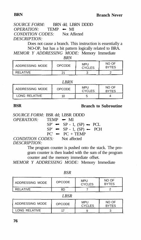
BRN Branch Never
SOURCE FORM: BRN dd; LBRN DDDD OPERATION: TEMP MI CONDITION CODES: Not Affected DESCRIPTION:
Does not cause a branch. This instruction is essentially a NO-OP, but has a bit pattern logically related to BRA.
MEMOR Y ADDRESSING MODE: Memory Immediate BRN
ADDRESSING MODE
RELATIVE
OPCODE
21
MPU CYCLES
3
NO OF BYTES
2
LBRN
ADDRESSING MODE
LONG RELATIVE
OPCODE
10
MPU CYCLES
5
NO OF BYTES
4
BSR Branch to Subroutine
SOURCE FORM: BSR dd; LBSR DDDD OPERATION: TEMP MI
SP' SP - 1, (SP) PCL SP' SP - 1, (SP) PCH PC' PC + TEMP
CONDITION CODES: Not affected DESCRIPTION:
The program counter is pushed onto the stack. The program counter is then loaded with the sum of the program counter and the memory immediate offset.
MEMOR Y ADDRESSING MODE: Memory Immediate
BSR
ADDRESSING MODE
RELATIVE
OPCODE
8D
MPU CYCLES
7
NO OF BYTES
2
LBSR
ADDRESSING MODE
LONG RELATIVE
OPCODE
17
MPU CYCLES
9
NO OF BYTES
3
76

BVC Branch on Overflow Clear
SOURCE FORM: BVC dd; LBVC DDDD OPERATION: TEMP MI
if V = 0 then PC' PC + TEMP CONDITION CODES: Not Affected DESCRIPTION:
Tests the state of the V bit and causes a branch if the V bit is clear. That is, branch if the two's complement result was valid.
MEMOR Y ADDRESSING MODE: Memory Immediate COMMENTS:
Used after an operation on two's complement binary values, this instruction will "branch if there was no overflow."
BVC
ADDRESSING MODE
RELATIVE
OPCODE
28
MPU CYCLES
3
NO OF BYTES
2
LBVC
ADDRESSING MODE
LONG RELATIVE
OPCODE
10
MPU CYCLES
5(6)
NO OF BYTES
4
BVS Branch on Overflow Set
SOURCE FORM: BVS dd; LBVS DDDD OPERATION: TEMP MI
if V = 1 then PC' PC + TEMP CONDITION CODES: Not Affected DESCRIPTION:
Tests the state of the V bit and causes a branch if the V bit is set. That is, branch if the two's complement result was invalid.
MEMORY ADDRESSING MODE: Memory Immediate COMMENTS:
Used after an operation on two's complement binary values, this instruction will "branch if there was an overflow." This instruction is also used after ASL or LSL to detect binary floating-point normalization.
77

BVS
ADDRESSING MODE
RELATIVE
OPCODE
29
MPU CYCLES
3
NO OF BYTES
2
LBVS
CLR Clear SOURCE FORM: CLR Q OPERATION: TEMP M
M 001 6 CONDITION CODES:
H: Not affected N: Cleared Z: Set V: Cleared C: Cleared
DESCRIPTION: ACCX or M is loaded with 00000000. The C-flag is cleared for 6800 compatibility.
CLRA
ADDRESSING MODE
INHERENT
OPCODE
4 F
MPU CYCLES
2
NO OF BYTES
1
CLRB
ADDRESSING MODE
INHERENT
OPCODE
5F
MPU CYCLES
2
NO OF BYTES
1
78
ADDRESSING MODE
LONG RELATIVE
OPCODE
10
MPU CYCLES
5(6)
NO OF BYTES
4

CLR
ADDRESSING MODE
DIRECT EXTENDED INDEXED
OPCODE
0F 7F 6F
MPU CYCLES
6 7 6+
NO OF BYTES
2 3 2+
CMP Compare Memory from a Register - 8 Bits SOURCE FORM; CMPA P; CMPB P OPERATION: TEMP R - M [i.e., TEMP R + + 1] CONDITION CODES: H: Undefined N: Set if bit 7 of the result is Set. Z: Set if all bits of the result are Clear. V: Set if the operation caused an 8-bit two's complement
overflow C: Set if the subtraction did not cause a carry from bit 7 in the
ALU
DESCRIPTION: Compares the contents of M from the contents of the specified register and sets appropriate condition codes. Neither M nor R is modified. The C flag represents a borrow and is set inverse to the resulting binary carry.
REGISTER ADDRESSING: Accumulator FLAG RESULTS:
(N V) = 1 R XT. M(2's comp) C = 1 R .LO. M (unsigned) Z = 1 R .EQ. M
CMPA
ADDRESSING MODE
DIRECT EXTENDED IMMEDIATE INDEXED
OPCODE
91 B1 81 A1
MPU CYCLES
4 5 2 4+
NO OF BYTES
2 3 2 2+
CMPB
ADDRESSING MODE
DIRECT EXTENDED IMMEDIATE INDEXED
OPCODE
D1 F1 C1 E1
MPU CYCLES
4 5 2 4+
NO OF BYTES
2 3 2 2+
79
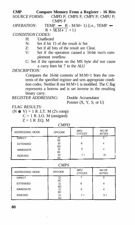
CMP Compare Memory From a Register - 16 Bits SOURCE FORMS: CMPD P; CMPX P, CMPY P; CMPU P;
CMPS P OPERATION: TEMP R - M:M+ 1) (i.e., TEMP
R + +1) CONDITION CODES:
H: Unaffected N: Set if bit 15 of the result is Set Z: Set if all bits of the result are Clear. V: Set if the operation caused a 16-bit two's com
plement overflow. C: Set if the operation on the MS byte did not cause
a carry from bit 7 in the ALU DESCRIPTION:
Compares the 16-bit contents of M:M+1 from the contents of the specified register and sets appropriate condition codes. Neither R nor M:M+1 is modified. The C flag represents a borrow and is set inverse to the resulting binary carry.
REGISTER ADDRESSING: Double Accumulator Pointer (X, Y, S, or U)
FLAG RESULTS: (N V) = 1 R .LT. M (2's comp)
C = 1 R .LO. M (unsigned) Z = 1 R .EQ. M
CMPD
ADDRESSING MODE
DIRECT
EXTENDED
IMMEDIATE
INDEXED
OPCODE
10 93 10 B3 10 83 10 A3
MPU CYCLES
7
8
5
7 +
NO OF BYTES
3
4
4
3+
CMPS
ADDRESSING MODE
DIRECT
EXTENDED
IMMEDIATE
INDEXED
OPCODE
11 9C 11 BC 11 8C 11 AC
MPU CYCLES
7
8
5
7 +
NO OF BYTES
3
4
4
3 +
80

CMPU ADDRESSING MODE
DIRECT
EXTENDED
IMMEDIATE
INDEXED
OPCODE
11 93 11 B3 11 83 11 A3
MPU CYCLES
7
8
5
7+
NO OF BYTES
3
4
4
3+
CMPX
ADDRESSING MODE
DIRECT EXTENDED IMMEDIATE INDEXED
OPCODE
9C BC 8C AC
MPU CYCLES
6 7 4 6+
NO OF BYTES
2 3 3 2+
CMPY
ADDRESSING MODE
DIRECT
EXTENDED
IMMEDIATE
INDEXED
OPCODE
10 9C 10 BC 10 8C 10 AC
MPU CYCLES
7
8
5
7+
NO OF BYTES
3
4
4
3+
COM Complement SOURCE FORM: COM Q OPERATION: M' O + CONDITION CODES:
H: Not affected N: Set if bit 7 of the result is Set Z: Set if all bits of the result are Clear V: Cleared C: Set
DESCRIPTION: Replaces the contents of M or ACCX with its one's complement (also called the logical complement). The carry flag is set for 6800 compatibility.
81
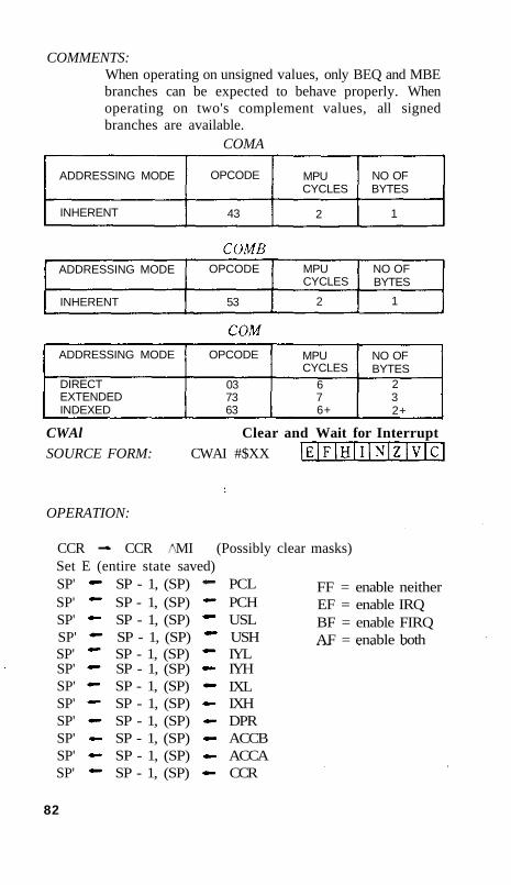
COMMENTS: When operating on unsigned values, only BEQ and MBE branches can be expected to behave properly. When operating on two's complement values, all signed branches are available.
COMA
82
ADDRESSING MODE
INHERENT
OPCODE
53
MPU CYCLES
2
NO OF BYTES
1
ADDRESSING MODE
INHERENT
OPCODE
43
MPU CYCLES
2
NO OF BYTES
1
ADDRESSING MODE
DIRECT EXTENDED INDEXED
OPCODE
03 73 63
MPU CYCLES
6 7 6+
NO OF BYTES
2 3 2+
SP' SP' SP' SP' SP' SP' SP' SP' SP' SP' SP' SP'
SP - 1, (SP) SP - 1, (SP) SP - 1, (SP) SP - 1, (SP) SP - 1, (SP) SP - 1, (SP) SP - 1, (SP) SP - 1, (SP) SP - 1, (SP) SP - 1, (SP) SP - 1, (SP) SP - 1, (SP)
PCL PCH USL USH IYL IYH IXL IXH DPR ACCB ACCA CCR
FF = enable neither EF = enable IRQ BF = enable FIRQ AF = enable both
CCR CCR MI (Possibly clear masks) Set E (entire state saved)
CWAl Clear and Wait for Interrupt SOURCE FORM: CWAI #$XX
OPERATION:

CONDITION CODES: Possibly cleared by the immediate byte.
DESCRIPTION: The CWAI instruction ANDs an immediate byte with the condition code register which may clear interrupt maskbit(s). It stacks the entire machine state on the hardware stack and then looks for an interrupt. When a nonmasked interrupt occurs, no further machine state will be saved before vectoring to the interrupt handling routine. This instruction replaced the 6800's CLI WAI sequence, but does not tri-state the buses.
ADDRESSING MODE: Memory Immediate COMMENTS:
An FIRQ interrupt may enter its interrupt handler with its entire machine state saved. The RTI will automatically return the entire machine state after testing the E bit of the recovered CCR.
CWAI
ADDRESSING MODE
INHERENT
OPCODE
3C
MPU CYCLES
20
NO OF BYTES
2
DA Decimal Addition Adjust SOURCE FORM: DAA OPERATION: ACCA' ACCA + CF(MSN):CF(LSN)
where CF is a Correction Factor, as follows: The C F . for each nybble (BCD) digit) is determined separately, and is either 6 or 0. Least Significant Nybble
CF(LSN) = 6 if 1) H = 1 or 2) LSN > 9
Most Significant Nybble CF(MSN)=6 if 1) C = 1
or 2) MSN > 9 or 3) MSN > 8 and LSN > 9
CONDITION CODES: H: Not affected N: Set if MSB of result is Set Z: Set if all bits of the result are Clear V: Not defined
83

C: Set if the operation caused a carry from bit 7 in the ALU, or if the carry flag was Set before the operation.
DESCRIPTION: The sequence of a single-byte add instruction on ACCA (either ADDA or ADCA) and a following DAA instruction results in a BCD addition with appropriate carry flag. Both values to be added must be in proper BCD form (each nybble such that 0 nybble 9). Multiple-precision additions must add the carry generated by this DA into the next higher digit during the add operation immediately prior to the next DA.
ADDRESSING MODE: ACCA
DAA
ADDRESSING MODE
INHERENT
OPCODE
19
MPU CYCLES
2
NO OF BYTES
1
DEC Decrement SOURCE FORM: DEC Q OPERATION: M' M - 1 (i.e., M' M + FF16 )
CONDITION CODES: H: Not affected N: Set if bit 7 of result is Set Z: Set if all bits of result are Clear V: Set if the original operand was 10000000 C: Not affected
DESCRIPTION: Subtract one from the operand. The carry flag is not affected, thus allowing DEC to be a loopcounter in multiple-precision computations.
COMMENTS: When operating on unsigned values only BEQ and BNE branches can be expected to behave consistently. When operating on two's complement values, all signed
branches are available. DECA
ADDRESSING MODE
INHERENT
OPCODE
4A
MPU CYCLES
2
NO OF BYTES
1
84

DECB
ADDRESSING MODE
INHERENT
OPCODE
5A
MPU CYCLES
2
NO OF BYTES
1
DEC
ADDRESSING MODE
DIRECT EXTENDED INDEXED
OPCODE
0A 7A 6A
MPU CYCLES
6 7 6+
NO OF BYTES
2 3 2 +
EOR Exclusive Or SOURCE FORMS: EORA P; EORB P OPERATION: R' R M CONDITION CODES:
H: Not affected N: Set if bit 7 of result is Set Z: Set if all bits of result are Clear V: Cleared C: Not affected
DESCRIPTION: The contents of memory is exclusive—ORed into an 8-bit register.
REGISTER ADDRESSING MODES: Accumulator
EORA
ADDRESSING MODE
DIRECT EXTENDED IMMEDIATE INDEXED
OPCODE
9B B8 88 A8
MPU CYCLES
4 5 2 4+
NO OF BYTES
2 3 2 2+
85
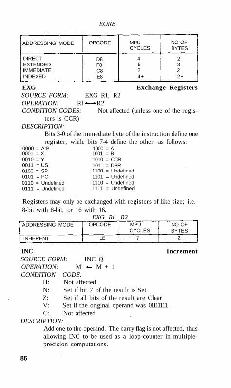
EORB
ADDRESSING MODE
DIRECT EXTENDED IMMEDIATE INDEXED
OPCODE
D8 F8 C8 E8
MPU CYCLES
4 5 2 4+
NO OF BYTES
2 3 2 2+
EXG Exchange Registers SOURCE FORM: EXG Rl, R2 OPERATION: Rl R2 CONDITION CODES: Not affected (unless one of the regis
ters is CCR) DESCRIPTION:
Bits 3-0 of the immediate byte of the instruction define one register, while bits 7-4 define the other, as follows:
0000 = A:B 0001 = X 0010 = Y 0011 = US 0100 = SP 0101 = PC 0110 = Undefined 0111 = Undefined
1000 = A 1001 = B 1010 = CCR 1011 = DPR 1100 = Undefined 1101 = Undefined 1110 = Undefined 1111 = Undefined
Registers may only be exchanged with registers of like size; i.e. 8-bit with 8-bit, or 16 with 16.
EXG Rl, R2 ADDRESSING MODE
INHERENT
OPCODE
1E
MPU CYCLES
7
NO OF BYTES
2
INC Increment SOURCE FORM: INC Q OPERATION: M' M + 1 CONDITION CODE:
H: Not affected N: Set if bit 7 of the result is Set Z: Set if all bits of the result are Clear V: Set if the original operand was 01111111. C: Not affected
DESCRIPTION: Add one to the operand. The carry flag is not affected, thus allowing INC to be used as a loop-counter in multiple-precision computations.
86

COMMENTS: When operating on unsigned values, only the BEQ and BNE branches can be expected to behave consistently. When operating on two's complement values, all signed branches are correctly available.
INCA
ADDRESSING MODE
INHERENT
OPCODE
4C
MPU CYCLES
2
NO OF BYTES
1
INCB
ADDRESSING MODE
INHERENT
OPCODE
5C
MPU CYCLES
2
NO OF BYTES
1
INC
ADDRESSING MODE
DIRECT EXTENDED INDEXED
OPCODE
0C 7C 6C
MPU CYCLES
6 7 6+
NO OF BYTES
2 3 2+
JMP Jump to Effective Address SOURCE FORM: JMP OPERATION: PC' EA CONDITION CODES: Not affected DESCRIPTION:
Program control is transferred to the location equivalent to the effective address.
JMP
ADDRESSING MODE
DIRECT EXTENDED INDEXED
OPCODE
0E 7E 6E
MPU CYCLES 3 4 3+
NO OF BYTES 2 3 2+
JSR Jump to Subroutine at Effective Address SOURCE FORM: JSR OPERATION: SP' SP - 1, (SP) PCL
SP' SP - 1, (SP) PCH PC' EA
CONDITION CODES: Not affected DESCRIPTION:
Program control is transferred to the Effective Address after storing the return address on the hardware stack.
87

JSR
ADDRESSING MODE
DIRECT EXTENDED INDEXED
OPCODE
9D BD AD
MPU CYCLES 7 8 7+
NO OF BYTES 2 3 2+
LD Load Register from Memory—8 Bit SOURCE FORMS: LDA P; LDB P OPERATION: R' M CONDITION CODES:
H: Not affected N: Set if bit of loaded data is Set Z: Set if all bits of loaded data are Clear V: Cleared C: Not affected
DESCRIPTION: Load the contents of the addressed memory into the register.
REGISTER ADDRESSING MODE: Accumulator LDA
LD Load Register from Memory—16 Bit SOURCE FORM: LDD P; LDX P; LDY P; LDS P; LDU P OPERATION: R' M:M+1 CONDITION CODES:
H: Not affected N: Set if bit 15 of loaded data is Set Z: Set if all bits of loaded data are Clear V: Cleared C: Not affected
88
ADDRESSING MODE
DIRECT EXTENDED IMMEDIATE INDEXED
OPCODE
96 B6 86, A6
MPU CYCLES 4 5 2 4+
NO OF BYTES 2 3 2 2+
ADDRESSING MODE
DIRECT EXTENDED IMMEDIATE INDEXED
OPCODE
D6 F6 C6 E6
MPU CYCLES
4 5 2 4 +
NO OF BYTES
2 3 2 2+
LDB

DESCRIPTION: Load the contents of the addressed memory (two consecutive memory locations) into the 16-bit register.
REGISTER ADDRESSING MODES: Double Accumulator Pointer (X, Y, S, or U)
LDD
ADDRESSING MODE
DIRECT EXTENDED IMMEDIATE INDEXED
OPCODE
DC FC CC EC
MPU CYCLES 5 6 3 5+
NO OF BYTES 2 3 3 2+
LDS ADDRESSING MODE
DIRECT
EXTENDED
IMMEDIATE
INDEXED
OPCODE
10 DE 10 FE 10 CE 10 EE
MPU CYCLES 6
7
4
6+
NO OF BYTES 3
4
4
3+
LDU ADDRESSING MODE
DIRECT EXTENDED IMMEDIATE INDEXED
OPCODE
DE FE CE EE
MPU CYCLES 5 6 3 5+
NO OF BYTES 2 3 3 2+
LDX ADDRESSING MODE
DIRECT EXTENDED IMMEDIATE INDEXED
OPCODE
9E BE 8E AE
MPU CYCLES 5 6 3 5+
NO OF BYTES 2 3 3 2+
LDY ADDRESSING MODE
DIRECT
EXTENDED
IMMEDIATE
INDEXED
OPCODE
10 9 F - 9 E 10 BE 10 8E 10 AE
MPU CYCLES 6
7
4
6+
NO OF BYTES 3
4
4
3+
89
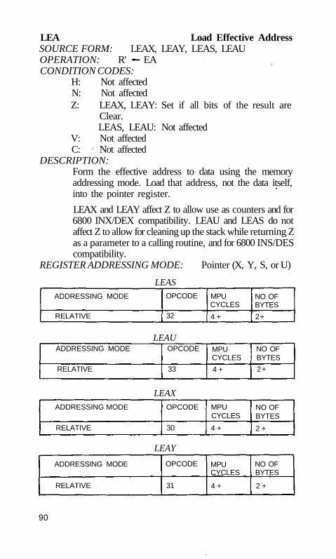
LEA Load Effective Address SOURCE FORM: LEAX, LEAY, LEAS, LEAU OPERATION: R' EA CONDITION CODES:
H: Not affected N: Not affected Z: LEAX, LEAY: Set if all bits of the result are
Clear. LEAS, LEAU: Not affected
V: Not affected C: Not affected
DESCRIPTION: Form the effective address to data using the memory addressing mode. Load that address, not the data itself, into the pointer register.
LEAX and LEAY affect Z to allow use as counters and for 6800 INX/DEX compatibility. LEAU and LEAS do not affect Z to allow for cleaning up the stack while returning Z as a parameter to a calling routine, and for 6800 INS/DES compatibility.
REGISTER ADDRESSING MODE: Pointer (X, Y, S, or U)
LEAS
ADDRESSING MODE
RELATIVE
OPCODE
32
LEAU ADDRESSING MODE
RELATIVE
OPCODE
33
LEAX
ADDRESSING MODE
RELATIVE
OPCODE
30
LEAY
ADDRESSING MODE
RELATIVE
OPCODE
31
MPU CYCLES
4 +
MPU CYCLES
4 +
MPU CYCLES
4 +
MPU CYCLES
4 +
NO OF BYTES
2+
NO OF BYTES
2+
NO OF BYTES
2 +
NO OF BYTES
2 +
90
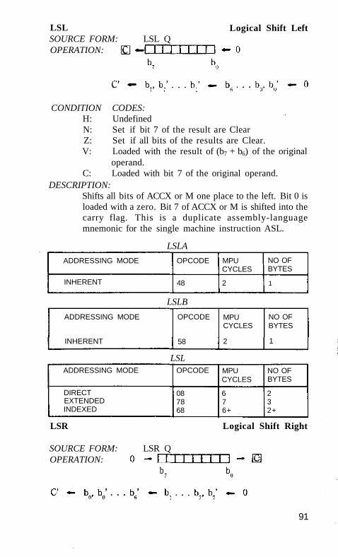
Logical Shift Left
CONDITION CODES: H: Undefined N: Set if bit 7 of the result are Clear Z: Set if all bits of the results are Clear. V: Loaded with the result of (b7 + b6) of the original
operand. C: Loaded with bit 7 of the original operand.
DESCRIPTION: Shifts all bits of ACCX or M one place to the left. Bit 0 is loaded with a zero. Bit 7 of ACCX or M is shifted into the carry flag. This is a duplicate assembly-language mnemonic for the single machine instruction ASL.
LSLA
ADDRESSING MODE
INHERENT
OPCODE
48
LSLB
ADDRESSING MODE
INHERENT
OPCODE
58
LSL ADDRESSING MODE
DIRECT EXTENDED INDEXED
OPCODE
08 78 68
MPU CYCLES
2
MPU CYCLES
2
MPU CYCLES
6 7 6+
NO OF BYTES
1
NO OF BYTES
1
NO OF BYTES
2 3 2+
LSR Logical Shift Right
SOURCE FORM: LSR Q OPERATION:
91
LSL SOURCE FORM: LSL Q OPERATION:

CONDITION CODES: H: Not affected N: Cleared Z: Set if all bits of the result are Clear V: Not affected C: Loaded with bit 0 of the original operand
DESCRIPTION: Performs a logical shift right on the operand. Shifts a zero into bit 7 and bit 0 into the carry flag. The 6800 processor also affects the V flag.
LSRA
ADDRESSING MODE
INHERENT
ADDRESSING MODE
INHERENT
ADDRESSING MODE
DIRECT EXTENDED INDEXED
OPCODE
44
LSRB
OPCODE
54
LSR
OPCODE
04 74 64
MPU CYCLES
2
MPU CYCLES
2
MPU CYCLES
6 7 6+
NO OF BYTES
1
NO OF BYTES
1
NO OF BYTES
2 3 2+
MUL Multiply Accumulators SOURCE FORM: MUL OPERATION: ACCA':ACCB' ACCA x ACCB CONDITION CODES:
H: Not affected N: Not affected Z: Set if all bits of the result are Clear V: Not affected C: Set if ACCB bit 7 of result is Set.
DESCRIPTION: Multiply the unsigned binary numbers in the accumulators and place the result in both accumulators. Unsigned multiply allows multiple-precision operations. The Carry flag allows rounding the MS byte through the sequence MUL, ADCA #0.
92

MUL
ADDRESSING MODE
INHERENT
OPCODE
3D
MPU CYCLES
11
NO OF BYTES
1
NEG Negate SOURCE FORM: NEG Q OPERATION: M' 0 - M (i.e., M' + l) CONDITION CODES:
H: Undefined N: Set if bit 7 of result is Set Z: Set if all bits of result are Clear V: Set if the original operand was 10000000 C: Set if the operation did not cause a carry
from bit 7 in the ALU. DESCRIPTION:
Replaces the operand with its two's complement. The C-flag represents a borrow and is set inverse to the resulting binary carry. Note that 8016 is replaced by itself and only in this case is V Set. The value 0016 is also replaced by itself, and only in this case is C cleared.
FLAG RESULTS: (N V) = 1 if 0 .LT. M (2's comp)
C = 1 if 0 .LO. M (unsigned) Z = 1 if 0 .EQ. M
NEGA
ADDRESSING MODE
INHERENT
ADDRESSING MODE
INHERENT
ADDRESSING MODE
DIRECT EXTENDED INDEXED
OPCODE
40
NEGB
OPCODE
50
NEG
OPCODE
00 70 60
MPU CYCLES
2
MPU CYCLES 2
MPU CYCLES
6 7 6+
NO OF BYTES 1
NO OF BYTES 1
NO OF BYTES
2 3 2+
93

NOP No Operation SOURCE FORM: NOP CONDITION CODES: Not affected DESCRIPTION:
This is a single-byte instruction that causes only the program counter to be incremented. No other registers or memory contents are affected.
NOP
ADDRESSING MODE
INHERENT
OPCODE
12
MPU CYCLES
2
NO OF BYTES
1
OR Inclusive OR Memory into Register SOURCE FORMS: ORA P; ORB P OPERATION: R' R v M CONDITION CODES:
H: Not affected N: Set if high order bit of result Set Z: Set if all bits of result are Clear V: Cleared C: Not affected
DESCRIPTION: Performs an "Inclusive OR" operation between the contents of ACCX and the contents of M and the result is stored in ACCX.
REGISTER ADDRESS MODE: Accumulator
ORA
ADDRESSING MODE
DIRECT EXTENDED IMMEDIATE INDEXED
OPCODE
9A BA 8A AA
MPU CYCLES
4 5 2 4 +
NO OF BYTES
2 3 2 2+
OREB
ADDRESSING MODE
DIRECT EXTENDED IMMEDIATE INDEXED
OPCODE
DA FA CA EA
MPU CYCLES
4 5 2 4 +
NO OF BYTES
2 3 2 2+
94

OR Inclusive OR Memory-Immediate into CCR SOURCE FORM: ORCC #XX OPERATION: R R v MI CONDITION CODES: CCR' CCR v MI DESCRIPTION:
Performs an "Inclusive OR" operation between the contents of CCR and the contents of MI, and the result is placed in CCR. This instruction may be used to Set interrupt masks (disable interrupts) or any other flag(s).
REGISTER ADDRESSNG MODE: CCR MEMOR Y ADDRESSING MODE: Memory Immediate
ORCC ADDRESSING MODE
IMMEDIATE
OPCODE
1A
MPU CYCLES
3
NO OF BYTES
2
PSHS Push Registers on the Hardware Stack SOURCE FORM: PSHS register list
PSHS #Label OPERATION: push order
if B7 of MI set, then:
if B6 of MI set, then;
if B5 of MI set, then:
if B4 of MI set, then:
if B3 of MI set, then: if B2 of MI set, then: if Bl of MI set, then: if B0 of MI set, then: CONDITION CODES: Not affected DESCRIPTION:
Any, all, any subset or none of the MPU registers are pushed onto the hardware stack, (excepting only the hardware stack pointer itself). MEMORY ADDRESSING MODE: Memory Immediate
PSHS
SP' SP' SP' SP' SP' SP' SP' SP' SP' SP' SP' SP'
SP - 1, (SP) SP - 1, (SP) SP - 1, (SP) SP - 1, (SP) SP - 1, (SP) SP - 1, (SP) SP - 1, (SP) SP - 1, (SP) SP - 1, (SP) SP - 1, (SP) SP - 1, (SP) SP - 1, (SP)
PCL PCH USL USH IYL IYH IXL IXH DPR ACCB ACCA CCR
ADDRESSING MODE
INHERENT
OPCODE
34
MPU CYCLES
5+
NO OF BYTES
2
95

PSHU Push Registers on the User Stack SOURCE FORM: PSHU register list PSHU #LABEL
push order OPERATION: if B7 of MI set, then:
if B6 of MI set, then:
if B5 of MI set, then:
if B4 of MI set, then:
if B3 of MI set, then: if B2 of MI set, then: if Bl of MI set, then: if B0 of MI set, then:
US' US' US' US' US' US' US' US' US' US' US' US'
US - 1, (US) US - 1, (US) US - 1, (US) US - 1, (US) US - 1, (US) US - 1, (US) US - 1, (US) US - 1, (US) US - 1, (US) US - 1, (US) US - 1, (US) US - 1, (US)
CONDITION CODES: Not affected
PCL PCH SPL SPH IYL IYH IXL IXH DPR ACCB ACCA CCR
DESCRIPTION: Any, all, any subset or none of the MPU registers are pushed onto the user stack (excepting only the user stack pointer itself).
MEMORY ADDRESSING MODE: Memory Immediate PSHU
ADDRESSING MODE
INHERENT
OPCODE
36
MPU CYCLES
5+4
NO OF BYTES
2
PULS Pull Registers from the Hardware Stack SOURCE FORM: PULS register list PULS #LABEL OPERATION: if if if if
if
if
if
B0 of MI set, Bl of MI set, B2 of MI set, B4 of MI set,
B5 of MI set,
B6 of MI set,
B7 of MI set,
then: then: then: then:
then:
then:
then:
CCR' ACCA' ACCB' IXH' IXL' IYH' IYL' USH' USL' PCH' PCL'
(SP), SP' (SP), SP' (SP), SP' (SP), SP' (SP), SP' (SP), SP' (SP), SP' (SP), SP' (SP), SP' (SP), SP' (SP), SP'
SP + 1 S P + 1 SP + 1 SP + 1 SP + 1 SP + 1 SP + 1 SP + 1 SP + 1 SP + 1 SP + 1
96
pull order

CONDITION CODES: May be pulled from stack, otherwise unaffected
DESCRIPTION: Any, all, any subset or none of the MPU registers are pulled from the hardware stack, (excepting only the hardware stack pointer itself). A single register may be "PULLED" with condition-flags set by loading auto-increment from stack (EX:LDA, S+).
MEMORY ADDRESSING MODE: Memory Immediate
PULS
ADDRESSING MODE OPCODE MPU CYCLES
NO OF BYTES
INHERENT 35 5+ 2
PULU Pull Registers from the User Stack SOURCE FORM: PULU register list
PULU #LABEL OPERATION: if B0 of MI set, then: if Bl of MI set, then: if B2 of MI set, then: if B3 of MI set, then: if B4 of MI set, then:
if B5 of MI set, then:
if B6 of MI set, then:
if B7 of MI set, then:
CCR' ACCA' ACCB' DPR' IXH' IXL' IYH' IYL' SPH' SPL' PCH' PCL'
(US), US' (US), US' (US), US' (US), US' (US), US' (US), US' (US), US' (US), US' (US), US' (US), US' (US), US (US), US
US + 1 US + 1 US + 1 US + 1 US + 1 US + 1 US + 1 US + 1 US + 1 US + 1 US + 1 US + 1
CONDITION CODES: May be pulled from stack, otherwise unaffected.
DESCRIPTION: Any all, any subset or none of the MPU registers are pulled from the user stack (excepting only the user stack pointer itself). A single register may be "PULLED" with condition-flags set by doing an auto-increment load from the stack (EX:LDX, U++))
MEMORY ADDRESSING MODE: Memory Immediate PULU
MPU CYCLES
ADDRESSING MODE
INHERENT
OPCODE
37
NO OF RYTES
5+
97
pull order
2

ROL SOURCE FORM: ROL Q
OPERATION:
Rotate Left
CONDITION CODES: H: Not affected N: Set if bit 7 of the result is Set Z: Set if all bits of the result are Clear V: Loaded with the result of (b7 b8) of the original operand. C: Loaded with bit 7 of the original operand DESCRIPTION:
Rotate all bits of the operand one place left through the carry flag; this is a 9-bit rotation.
ROLA ADDRESSING MODE
INHERENT
ADDRESSING MODE
INHERENT
ADDRESSING MODE
DIRECT EXTENDED INDEXED
OPCODE
49
ROLB OPCODE
59
ROL
OPCODE
09 79 69
MPU CYCLES
2
MPU CYCLES
2
MPU CYCLES
6 7 6+
NO OF BYTES
1
NO OF BYTES
1
NO OF BYTES
2 3 2+
ROR SOURCE FORM: ROR Q
Rotate Right
OPERATION:
CONDITION CODES: H: Not affected N: Set if bit 7 of result is Set Z: Set if all bits of result are Clear V: Not affected C: Loaded with bit 0 of the previous operand

DESCRIPTION: Rotates all bits of the operand right one place through the carry flag; this is a nine-bit rotation. The 6800 processor also affects the V flag.
RORA
if CCR bit E is SET then:
if CCR bit E is CLEAR then:
ACCA' ACCB' DPR' IXH' IXL' IYH' IYL' USH' USL' PCH' PCL'
PCH' PCL'
(SP), SP' (SP), SP' (SP), SP' (SP), SP' (SP), SP' (SP), SP' (SP), SP' (SP), SP' (SP), SP' (SP), SP' (SP), SP'
(SP), SP' (SP), SP'
SP + 1 SP + 1 SP + 1 SP + 1 SP + 1 SP + 1 SP + 1 SP + 1 SP + 1 SP + 1 SP + 1
SP + 1 SP + 1
CONDITION CODES: Recovered from stack DESCRIPTION:
The saved machine state is recovered from the hardware stack and control is returned to the interrupted program. If the recovered E bit is CLEAR, it indicates that only a subset of the machine state was saved (return address and condition codes) and only that subset is to be recovered.
99
ADDRESSING MODE
INHERENT
OPCODE
46
MPU CYCLES
2
NO OF BYTES
1
ADDRESSING MODE
INHERENT
OPCODE
56
MPU CYCLES
2
NO OF BYTES
1
ADDRESSING MODE
DIRECT EXTENDED INDEXED
OPCODE
06 76 66
MPU CYCLES
6 7 6 +
NO OF BYTES
2 3 2+
RTI Return from Interrupt SOURCE FORM: RTI OPERATION: CCR' (SP), SP' SP + 1
RORB
ROR
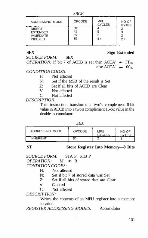
SBCB
ADDRESSING MODE
DIRECT EXTENDED IMMEDIATE INDEXED
OPCODE
D2 F2 C2 E2
MPU CYCLES 4 5 2 4 +
NO OF BYTES 2 3 2 2 +
SEX Sign Extended SOURCE FORM: SEX OPERATION: If bit 7 of ACCB is set then ACCA' FFl6
else ACCA' 00l6
CONDITION CODES: H: Not affected N: Set if the MSB of the result is Set Z: Set if all bits of ACCD are Clear V: Not affected C: Not affected
DESCRIPTION: This instruction transforms a two's complement 8-bit value in ACCB into a two's complement 16-bit value in the double accumulator.
SEX
ADDRESSING MODE
INHERENT
OPCODE
1D
MPU CYCLES 2
NO OF BYTES 1
ST Store Register Into Memory—8 Bits
SOURCE FORM: STA P; STB P OPERATION: M' R CONDITION CODES:
H: Not affected N: Set if bit 7 of stored data was Set Z: Set if all bits of stored data are Clear V: Cleared C: Not affected
DESCRIPTION: Writes the contents of an MPU register into a memory location.
REGISTER ADDRESSING MODES: Accumulator
101

RTI
ADDRESSING MODE
INHERENT
OPCODE
3B
MPU CYCLES
6/15
NO OF BYTES
1
RTS Return from Subroutine SOURCE FORM: RTS OPERATION: PCH' (SP), SP' SP + 1
PCL' (SP), SP' SP + 1 CONDITION CODES: Not affected DESCRIPTION:
Program control is returned from the subroutine to the calling program. The return address is pulled from the stack.
RTS
ADDRESSING MODE
INHERENT
OPCODE
39
MPU CYCLES
5
NO OF BYTES
1
SBC Subtract with Borrow SOURCE FORMS: SBCA P; SBCB P OPERATION: R' R - M - C (i.e., R' R+ + CONDITION CODES:
H: Undefined N: Set if bit 7 of the result is Set Z: Set if all bits of the result are Clear V: Set if the operation causes an 8-bit two's comple
ment overflow C: Set if the operation did not cause a carry from bit 7
in the ALU
DESCRIPTION: Subtracts the contents of M and the borrow (in the carry flag)
from the contents of an 8-bit register, and places the result in that register. The C flag represents a borrow and is set inverse to the resulting binary carry. REGISTER ADDRESSING MODE: Accumulator
SBCA ADDRESSING MODE
DIRECT EXTENDED IMMEDIATE INDEXED
OPCODE
92 B2 82 A2
MPU CYCLES
4 5 2 4 +
NO OF BYTES
2 3 2 2+
100

STA
ADDRESSING MODE
DIRECT EXTENDED INDEXED
OPCODE
97 B7 A7
MPU CYCLES
4 5 4 +
NO OF BYTES
2 3 2+
STB ADDRESSING MODE
DIRECT EXTENDED INDEXED
OPCODE
D7 F7 E7
MPU CYCLES
4 5 4 +
NO OF BYTES
2 3 2+
ST Store Register Into Memory—16-Bi SOURCE FORM: STD P; STX P; STY P; STS P; STU P OPERATION: M':M+1' R CONDITION CODES:
H: Not affected N: Set if bit 15 of stored data was Set Z: Set if all bits of stored data are Clear V: Cleared C: Not affected
DESCRIPTION: Write the 16 bit register into consecutive memory locations
REGISTER ADDRESSING MODES: Double Accumulator Pointer (X, Y, S, or U)
STD
ADDRESSING MODE
DIRECT EXTENDED INDEXED
OPCODE
DD FD ED
MPU CYCLES
5 6 5+
NO OF BYTES
2 3 2+
STS
ADDRESSING MODE
DIRECT
EXTENDED
INDEXED
OPCODE
10 DF 10 FF 10 EF
MPU CYCLES
6
7
6+
NO OF BYTES
3
4
3 +
102
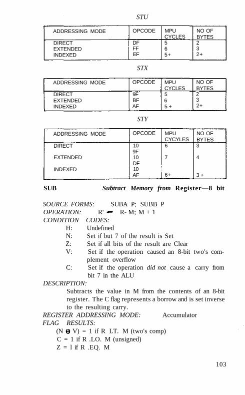
STU
ADDRESSING MODE
DIRECT EXTENDED INDEXED
OPCODE
DF FF EF
MPU CYCLES 5 6 5+
NO OF BYTES 2 3 2+
STX
ADDRESSING MODE
DIRECT EXTENDED INDEXED
OPCODE
9F BF AF
MPU CYCLES 5 6 5 +
NO OF BYTES 2 3 2+
STY
ADDRESSING MODE
DIRECT
EXTENDED
INDEXED
OPCODE
10 9F 10 DF 10 AF
MPU CYCYLES 6
7
6+
NO OF BYTES 3
4
3 +
SUB Subtract Memory from Register—8 bit
SOURCE FORMS: SUBA P; SUBB P OPERATION: R' R- M; M + 1 CONDITION CODES:
H: Undefined N: Set if but 7 of the result is Set Z: Set if all bits of the result are Clear V: Set if the operation caused an 8-bit two's com
plement overflow C: Set if the operation did not cause a carry from
bit 7 in the ALU DESCRIPTION:
Subtracts the value in M from the contents of an 8-bit register. The C flag represents a borrow and is set inverse to the resulting carry.
REGISTER ADDRESSING MODE: Accumulator FLAG RESULTS:
(N V) = 1 if R LT. M (two's comp) C = 1 if R .LO. M (unsigned) Z = l if R .EQ. M
103

SUBA ADDRESSING MODE
DIRECT EXTENDED IMMEDIATE INDEXED
OPCODE
90 BC 80 A0
MPU CYCLES
4 5 2 4 +
NO OF BYTES
2 3 2 2 +
SUBB
ADDRESSING MODE
DIRECT EXTENDED IMMEDIATE INDEXED
OPCODE
DO F0 CO EO
MPU CYCLES 4 5 2 4 +
NOOF BYTES 2 3 2 2+
SUB Subtract Memory from Register—16-Bit SOURCE FORM: SUBD P OPERATION: R' R - M:M+1 [i.e., R; R + + l]
CONDITION CODES: H: Unaffected N: Set if bit 15 of result is Set Z: Set if all bits of result are Clear V: Set if the operation caused a 16-bit two's
complement overflow. C: Set if the operation on the MS byte did not cause
a carry from bit 7 in the ALU DESCRIPTION:
This information subtracts the value in M:M+1 from the 16-bit accumulator. The C flag represents a borrow and is set inverse to the resulting binary carry.
REGISTER ADDRESSING MODE: Double Accumulator SUBTRACT SETS:
(N V) = 1 if R .LT. M (two's comp) C = 1 if R .LO. M (unsigned) Z = 1 if R .EQ. M
SUBD ADDRESSING MODE
DIRECT EXTENDED IMMEDIATE INDEXED
OPCODE
93 B3 83 A3
MPU CYCLES 6 7 4 6+
NO OF BYTES 2 3 3 2+
104
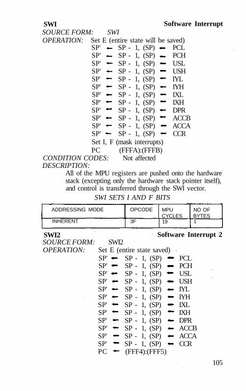
SWI SOURCE FORM: SWI OPERATION: Set E (entire state will be saved)
Software Interrupt
SP' SP' SP' SP' SP' SP' SP' SP' SP' SP' SP' SP'
SP - 1, (SP) SP - 1, (SP) SP - 1, (SP) SP - 1, (SP) SP - 1, (SP) SP - 1, (SP) SP - 1, (SP) SP - 1, (SP) SP - 1, (SP) SP - 1, (SP) SP - 1, (SP) SP - 1, (SP)
PCL PCH USL USH IYL IYH IXL IXH DPR ACCB ACCA CCR
Set I, F (mask interrupts) PC (FFFA):(FFFB)
CONDITION CODES: Not affected DESCRIPTION:
All of the MPU registers are pushed onto the hardware stack (excepting only the hardware stack pointer itself), and control is transferred through the SWI vector.
SWI SETS I AND F BITS
ADDRESSING MODE
INHERENT
OPCODE
3F
MPU CYCLES 19
NO OF BYTES 1
SWI2 Software Interrupt 2 SOURCE FORM: OPERATION: Set
SP' SP' SP' SP' SP' SP' SP' SP' SP' SP' SP' SP' PC
SWI2 E (entire state saved)
SP - 1, (SP) SP - 1, (SP) SP - 1, (SP) SP - 1, (SP) SP - 1, (SP) SP - 1, (SP) SP - 1, (SP) SP - 1, (SP) SP - 1, (SP) SP - 1, (SP) SP - 1, (SP) SP - 1, (SP) (FFF4):(FFF5)
PCL PCH USL USH IYL IYH IXL IXH DPR ACCB ACCA CCR
105
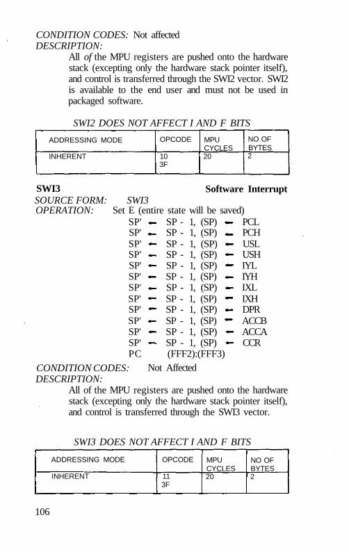
CONDITION CODES: Not affected DESCRIPTION:
All of the MPU registers are pushed onto the hardware stack (excepting only the hardware stack pointer itself), and control is transferred through the SWI2 vector. SWI2 is available to the end user and must not be used in packaged software.
SWI2 DOES NOT AFFECT I AND F BITS
ADDRESSING MODE
INHERENT
OPCODE
10 3F
MPU CYCLES 20
NO OF BYTES 2
SWI3 SOURCE FORM: SWI3
Software Interrupt
OPERATION: Set E (entire state will be saved) SP' SP' SP' SP' SP' SP' SP' SP' SP' SP' SP' SP' PC
CONDITION CODES:
SP - 1, (SP) SP - 1, (SP) SP - 1, (SP) SP - 1, (SP) SP - 1, (SP) SP - 1, (SP) SP - 1, (SP) SP - 1, (SP) SP - 1, (SP) SP - 1, (SP) SP - 1, (SP) SP - 1, (SP) (FFF2):(FFF3)
Not Affected
PCL PCH USL USH IYL IYH IXL IXH DPR ACCB ACCA CCR
DESCRIPTION: All of the MPU registers are pushed onto the hardware stack (excepting only the hardware stack pointer itself), and control is transferred through the SWI3 vector.
SWI3 DOES NOT AFFECT I AND F BITS
ADDRESSING MODE
INHERENT
OPCODE
11 3F
MPU CYCLES 20
NO OF BYTES 2
106

SYNC Synchronize to External Event SOURCE FORM: SYNC OPERATION: Stop processing instructions CONDITION CODES: Unaffected DESCRIPTION:
When a SYNC instruction is executed, the MPU enters a SYNCING state, stops processing instructions and waits on an interrupt. When an interrupt occurs, the SYNCING state is cleared and processing continues. IF the interrupt is enabled, and the interrupt lasts 3 cycles or more, the processor will perform the interrupt routine. If the interrupt is masked or is shorter than 3 cycles long, the processor simply continues to the next instruction (without stacking registers). While SYNCING, the address and data buses are tri-state.
COMMENTS: This instruction provides software synchronization with a hardware process. Consider the high-speed acquisition of data:
FOR DATA
FAST SYNC WAIT FOR DATA interrupt!
LDA DISC DATA FROM DISC AND CLEAR INTERRUPT
STA ,X+ PUT IN BUFFER DECB COUNT IT, DONE? BNE FAST GO AGAIN IF NOT.
The SYNCING state is cleared by any interrupt, and any enabled interrupt will probably destroy the transfer (this may be used to provide MPU response to an emergency condition). The same connection used for interrupt-driven I/O service may thus be used for high-speed data transfers by setting the interrupt mask and using SYNC.
SYNC
ADDRESSING MODE
INHERENT
OPCODE
13
MPU CYCLES > = 2
NO OF BYTES 1
107

TFR Transfer Register to Register SOURCE FORM: TFR R1, R2
OPERATION: R2 R1
CONDITION CODES: Not affected (Unless R2 = CCR) DESCRIPTION:
Bits 7-4 of the immediate byte of the instruction define the source register, while bits 3-0 define the destination register, as follows:
0000 = A:B 0001 = X 0010 = Y 0011 = US 0100 = SP 0101 =PC 0110 = Undefined 0111 = Undefined
1000 = A 1001 = B 1010 =CCR 1011 = DPR 1100 = Undefined 1101 = Undefined 1110 = Undefined 1111= Undefined
Registers may only be transferred between registers of like size; i.e., 8-bit to 8-bit, and 16 to 16.
TFR R1.R2
ADDRESSING MODE
INHERENT
OPCODE
1F
MPU CYCLES 7
NO OF BYTES 2
Test TST SOURCE FORM: TST Q OPERATION: TEMP M - 0 CONDITION CODES:
H: Not affected N: Set if bit 7 of the result is Set Z: Set if all bits of the result are Clear V: Cleared C: Not affected
DESCRIPTION: Set condition code flags N and Z according to the contents of M, and clear the V flag. The 6800 processor clears the C flag.
COMMENTS: The TST instruction provides only minimum information when testing unsigned values; since no unsigned value is less than zero, BLO and BLS have no utility. While BHI could be used after TST, it provides exactly the same control as BNE, which is preferred. The signed branches are available.
108

TSTA
ADDRESSING MODE
INHERENT
OPCODE
4D
MPU CYCLES
NO OF BYTES
2 1
TSTB
ADDRESSING MODE
INHERENT
OPCODE
5D
MPU CYCLES
2
NO OF BYTES
1
TST
ADDRESSING MODE
DIRECT EXTENDED INDEXED
OPCODE
OD 7D 6D
MPU CYCLES
6 7 6+
NO OF BYTES
2 3 2+
HARDWARE INSTRUCTION FIRQ Fast Interrupt Request
OPERATION: if F bit CLEAR, then: SP' SP - 1, (SP) PCL SP' SP - 1, (SP) PCH Clear E (subset state is saved) SP' SP - 1, (SP) CCR Set if, I (mask further interrupts) PC' (FFF6):(FFF7)
CONDITION CODES: Not affected DESCRIPTION:
A low level on the FIRQ input with the F bit clear causes this interrupt sequence to occur at the end of the current instruction. The program counter and condition code register are pushed onto the hardware stack. Program control is transferred through the FIRQ vector. An RTI returns to the original task. It is possible to enter an FIRQ handler with the entire state saved if the FIRQ occurs after CWAI.
ADDRESSING MODE: Absolute Indirect COMMENTS:
An IRQ interrupt, having lower priority than the FIRQ, is prevented from interrupting the FIRQ handling routine by automatic setting of the I flag. This mask bit could then
109

be reset if priority was not desired, The IRQ allows operations on memory, TST, INC, DEC, etc., without the overhead of saving the entire machine state on the stack.
HARDWARE INSTRUCTION IRQ Interrupt Request OPERATION: IFF I bit CLEAR, then:
SP' SP' SP' SP' SP' SP' SP' SP'
SP - 1, (SP) SP - 1, (SP) SP - 1, (SP) SP - 1, (SP) SP - 1, (SP) SP - 1, (SP) SP - 1, (SP) SP - 1, (SP)
PCL PCH USL USH IYL IYH IXL IXH
110
CONDITION CODES: Not affected DESCRIPTION:
If the IRQ mask bit I is clear, a low level on the IRQ input causes this interrupt sequence to occur at the end of the current instruction. Control is returned to the interrupted program via an RTI. An FIRQ may interrupt an IRQ handling routine and be recognized anytime after the IRQ vector is taken.
ADDRESSING MODE: Absolute Indirect
HARDWARE INSTRUCTION NMI Non-Maskable Interrupt
OPERATION:
SP' SP' SP' SP' SP' SP' SP' SP' SP' SP' SP'
SP - 1, (SP) SP - 1, (SP) SP - 1, (SP) SP - 1, (SP) SP - 1, (SP) SP - 1, (SP) SP - 1, (SP) SP - 1, (SP) SP - 1, (SP) SP - 1, (SP) SP - 1, (SP)
PCL PCH USL USH IYL IYH IXL IXH DPR ACCB ACCA
Set E (entire state saved) SP' SP - 1, (SP) CCR Set I (mask further IRQ interrupts) PC' (FFF8):(FFF9)

CONDITION CODES: Not affected DESCRIPTION:
A negative edge on the NMI input causes all of the MPU registers (except the hardware stack pointer SP) to be pushed onto the hardware stack, starting at the end of the current instruction. Program control is transferred through the NMI vector. Successive negative edges on the NMI input will cause successive NMI operations. The NMI operation is internally blocked by RESET, any NMI-edge will be latched, and the operation will occur after the first load into the stack pointer (LDS; TFR r,s; EXG r,s; etc.).
ADDRESSING MODE: Absolute Indirect
HARDWARE INSTRUCTION RESTART OPERATION: CCR' X1X1XXXX
DPR' 0016 PC (FFFE):(FFFF)
CONDITION CODES: Not affected DESCRIPTION:
The MPU is initialized (required after power-on) to start program execution.
ADDRESSING MODE: Absolute Indirect
111
SP' SP' SP'
SP - 1, (SP) SP - 1, (SP) SP - 1, (SP)
Set E (entire state save) SP' SP - 1, (SP)
DPR ACCB ACCA
CCR Set I, F (mask interrupts) PC' (FFFC):(FFFD)

MEK6809EA Assembler Motorola has not only developed the 6809D4 evaluation unit, but is supporting it with a variety of software. One piece of software available from Motorola is the MEK6809EA assembler. This is a specialized program that is designed to process source programs written in M6809 assembly language. This "source" is then translated into object programs that the firmware loaders on the D4 evaluation unit can understand.
The previous chapter gave you definitions to the various instruction codes that the 6809 understands and, in some cases, examples of an assembly code. I will attempt in this chapter to give you only the basics of the assembler. Should you desire to learn more, the supporting software and D4 unit should be purchased from Motorola, or the Radio Shack TRS-80 Color Computer or Videotex should be bought.
BASICS OF THE ASSEMBLER
The assembler, as stated before, performs operations on source code that contains specific operations which determine what will happen when the program executes as an object, or run-time, program. Some of these internals of the source file are operations such as instruction codes, or assembler directives, and labels—sometimes called symbolic names, special operators and special symbols. Directives, which are part of the assembler's operation, are special codes that are entered into the source file to tell the assembler to perform a specific operation.
112

Essentially, the role of the assembler is to translate source programs into object code in a format required by the systems' loader. As you will see in Chapter 6, this will be for the D4. The assembler is also used for archival purposes. Debugging the assembler provides a listing which contains all the information about the program in logical fashion.
TYPICAL REQUIREMENTS The assembler takes information in source form and trans
lates it into object form. To do this, however, certain rules are usually followed.
First, the source form of the program is a sequence of statements written in ASCII characters following conventions that the specific assembler requires. Each input source line is terminated with a carriage return. The source form usually consists of five fields:
• Sequence number. This is not always required, but is useful especially in the editing function.
• Label or an asterik (*) implying a comment. • Operation. • Operand. • Optional comment.
Sequence Number This is an option for programmer convenience for the
Motorola assembler. A sequence number can consist of up to five decimal digits but less than 65,536. When used, the sequence number must be followed by a space.
Label Field This field is right after the sequence number, or it can appear
as the first field. When an asterisk (*) is used, the line is considered by the assembler to be comment and is thus ignored. A blank indicates that the field is empty and the line contains no label.
The symbol is a special form of a label and has the following attributes:
• Usually consists of 1 to 6 characters. • Only the following are considered valid symbol charac
ters: A through Z, 0 through 9, "."—period, and a dollar sign "$". • A symbol must consist of either a period ".", or an
alphanumeric character as the first character.
113
• Certain symbols: A, B, D, X, Y, U, S, CC, PC, PCR and DP are reserved symbols used by the assembler and are never used in the label field.
When a symbol is used, it may occur only once in the label field. If it occurs in more than one label field, a reference to that symbol will cause an error, since the assembler will have no idea to what you are referring.
A typical label can be used in an equate statement, that unique statement that sets a label equal to a specific value. Some examples of labels are:
INCH EQU $FC00 .Gl LDA #$41
Operating Field
The operation field occurs directly after the label field in an assembly language source statement. This field consists of an operation code of three or four characters. Entries in the operation code field may be one of two types. Machine mnemonic operation code entries correspond directly to M6809 machine instructions. This operation code field includes the "A" or "B" character for the "dual" or "accumulator" addressing modes. Directives are special operation codes known to the assembler which control the assembly process rather than being translated directly to machine language.
The assembler searches for operation codes in the table of machine operation codes and directives. If not found, an error message is printed.
Operand Field
Interpretation of the operand field is dependent on the operation field. For the M6809 machine instructions, the operand field must specify the addressing mode. The operand field formats and the corresponding addressing modes are in Table 5-1.
Comment Field
The last field of an M6809 Assembly Language source line is the comment field. This field is optional and is ignored by the assembler except for being included in the listing. The comment field is separated from the operand field (or the operator field if there is no operand) by one or more blanks and may consist of any
114

Table 5 -1 . Operand Field Formats and Corresponding Addressing Modes.
M6809 Machine Instruction Operand Format Addressing Mode
inherent and accumulator direct or extended
(direct will be used if possible) immediate indexed (where "R" is an indexable register)
ASCII character. This field is important in documenting the operation of a program.
EXPRESSIONS
An expression is a combination of symbols and/or numbers separated by one of the arithmetic operators (+ , - , *, or / ) . The assembler evaluates expressions algebraically from left to right without parenthetical grouping. There is no precedence hierarchy among the arithmetic operators. A fractional result, or intermediate result obtained during the evaluation of an expression, will be truncated to an integer value.
Constants
Decimal: < number > Hexadecimal: $ < number > or < number > H (first digit in
latter case must be 0 - 9) Octal: @ < number > or < number > 0 or < number > Q Binary: % < number > or < number > B
ASCII Literals
' <character>: apostrophe followed by an ASCII character, except carriage return. The result is the numeric value for the ASCII character.
SYMBOLS
A symbol in an expression is similar to a symbol in the label field except that the value of the symbol is referenced instead of defined. An asterisk "*" is a special symbol recognized by the
no operand expression
# (expression) (expression), R
115

Table 5-2. Assembly Listing.
0001 0002 0004 00005 00006 00007 00008 00010 TOTAL TOTAL
PAGE
00001 00002 00004 00005 00006 00007 00008
00010
TOTAL TOTAL
2000 2000 10CE 2004 10AE 2007 10AF 200A 32
ERRORS WARNINGS
E0000 E4 84 16 2000
00000 00000
4 6 6 5
NAM ENDST OPT LLEN=80 ORG
START $2000 LDY +$F0000 STY S LEAS X END -10,X
001 ENDST1 *PROGRAM NOT INDICATING EXECUTION START*
2000 2000 10CE 2004 10AE 2007 10AF 200A 32
ERRORS WARNINGS
E000O E4 84 16
0000
0000 00000
6 6 5
NAM ENDST1 OPT LLEN ORG 140080
$2000 LDY +$E000 STY S LEAS X END -10,X
assembler and represents the value of the current location counter (first byte of an instruction), when used in the context of the symbol.
A 16-bit integer value is associated with each symbol. This value is used in place of the symbol during expression evaluation.
Table 5-3. Standard Format for Assembly Listings.
Column
1-5
7-10 12-15 17-23 25-26 28-33 35-39 41-48
50-Last Column
Contents
Source line 1 - 5 digit decimal counter kept by assembler. Current Location Counter value (in hex). Machine Operation Code (hex). Operand Machine Code (if any) (hex). Cycle Count of Execution Time (decimal). Label Field. Operation Field. Operand Field (longer operand extends into comment field). Comment Field.
116

The MEK6809EA assembler is a two-pass assembler. The symbol table is built on the first pass. Object records and listing are produced on the second pass. Certain expressions cannot be fully evaluated during the first pass because they may contain (forward) references to symbols which have not yet been defined. In some cases, a symbol may not be defined before being used in the second pass. Since the assembler cannot evaluate such symbols, these cases are treated as errors. Only one level of forward referencing is allowed.
ASSEMBLER LISTING
Assembler outputs include an assembly listing and an object program (Table 5-2). The assembly listing includes the source program as well as additional information generated by the assembler. Most lines in the listing correspond directly to a source statement. Lines which do not correspond directly to a source line include: page header line, error lines and expansion lines for the FCC, FDB and FCB directives. Most listing lines follow the standard format shown in Table 5-3.
117
Implementation of VTL-09 The implementation of BASIC that is to be presented in the next few pages is based on a design created by Gary Shannon and Frank McCoy for the MITs 680b microcomputer. Their implementation was named VTL-2 for Very Tiny Language, and permitted users of the 680b to have high-level language capability with only 1K bytes of working memory space. VTL-2, originally implemented, required only 768 bytes of memory and was written in such a manner to be ROMable.
As you proceed through this chapter, you will realize that the small BASIC-like language we are talking about is quite powerful. In fact, it most likely is still the most powerful small interpreter available today. The original copyright was 1977 for the 6800 version of VTL-2 and is still held by the Computer Store of Santa Monica, California. The following pages are designed to assist you in how to use what I call VTL-09.
DIRECT AND PROGRAM STATEMENTS
The statements that may be entered as input to the VTL-09 interpreter are of two types: the direct statement, which has no line number and is executed immediately after being entered; and the program statement, which requires line numbers used to build a program. Program statements are not executed until the program is run as opposed to the immediate execution of direct statements.
118

The design of VTL-09 is simple, making it ideal for the beginner and powerful enough for advanced purposes. An important feature, not found with other versions of VTL, is the inclusion of calls to permit loading and dumping of programs to tape. The implementation that is presented in this book is strictly for the Motorola 6809D4 unit which is designed to load at $2000 hex.
PRELIMINARY CONCEPTS
Line numbers must precede each program statement. The statements following the line number must be separated from the number by at least one space. As designed, each line must end with a carriage return and be less than 73 characters in length.
Typically, line numbers are incremented in steps of 10. This permits the addition of other statements if necessary. No line renumbering utility is included, so care must be taken when first beginning the program process.
Variables may be represented by any single alphabetic or special character such as !"#$%&'()=-+*:;?/ .><[]. Most of these are available for the user to define as he wishes. A few of the variable names, however, have been set aside for special purposes. These so-called system variables will be discussed in detail later.
The value assigned to a variable may be either a numeric value in the range 0-65535, or a single ASCII character, including control characters. Numeric and string values may be freely interchanged, in which case the characters are equivalent to the decimal value of their ASCII code representation. Thus, it becomes possible to add 1 to the letter A, giving as a result the letter B.
ARITHMETIC OPERATIONS
The arithmetic operations permitted for use in expressions are:
• • • • • • •
+ addition - subtraction * multiplication / division = test for equality > test for greater than or equal to < test for less than
119

The test operations—equal to, greater than or equal to and less than—all return a value of zero if the test fails and a value of one if the test is successful.
Expressions in VTL-09 may contain any number of variables or numeric values—literals—connected by any of the above operations. Parentheses may be used to alter the order of execution of the operations. If no parentheses are included, the operations proceed in strictly right to left order.
The value resulting from the expression must be assigned to some variable name. This is done with the equal sign. Note that the symbol has two meanings depending on where it occurs in the expression. The expression "A=B=C" means test b and c for equality. If they are equal put a one in A; if they are unequal, put a zero in A. Some of the examples of valid arithmetic expressions would be:
Y=A*(X*X)+B*X+C with left to right execution. This is equivalent to Y=(A*X*X+B)*X+C
Y=(A*X*X)+(B*X)+C which is equivalent o AX2+BX+C
Notice how the absence of parentheses around the quantity B*X in the first expression has completely altered its meaning. Keep the right to left order in mind, and when in doubt use parentheses to control the order of evaluation.
SYSTEM VARIABLES
In order to conserve space and to provide a more consistent syntax, VTL-09, like VTL-2 uses system variables to accomplish functions usually done with special key words in other languages. This convention is probably the single most important reason for its tiny size. These special variables are used for such functions as the BASIC PRINT, GOTO, GOSUB, RETURN, IF AND RANDOM functions.
Pound Sign
The system variable number or pound sign (#) represents the line number of the line being executed. Until the statement has been completed, it will contain the current line number. For example, the statement 100 A=# is equivalent to simply writing 100 A=100. After completion of a line, this variable will contain the number of the next line to be executed. If nothing is done to the variable, this will be the next line in the program text. If a state-
1 2 0
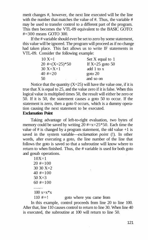
merit changes #, however, the next line executed will be the line with the number that matches the value of #. Thus, the variable # may be used to transfer control to a different part of the program. This then becomes the VTL-09 equivalent to the BASIC GOTO: #=300 means GOTO 300.
If the # variable should ever be set to zero by some statement, this value will be ignored. The program will proceed as if no change had taken place. This fact allows us to write IF statements in VTL-09. Consider the following example:
10 X=l Set X equal to 1 20 #=(X=25)*50 If X=25 goto 50 30 X=X+1 add 1 to x 40 #=20 goto 20 50 and so on
Notice that the quantity (X=25) will have the value one, if it is true that X is equal to 25, and the value zero if it is false. When this logical value is multiplied times 50, the result will either be zero or 50. If it is 50, the statement causes a goto 50 to occur. If the statement is zero, then a goto 0 occurs, which is a dummy operation causing the next statement to be executed. Exclamation Point
Taking advantage of left-to-right evaluation, two bytes of memory could be saved by writing 20 #=x=25*50. Each time the value of # is changed by a program statement, the old value +1 is saved in the system variable—exclamation point (!). In other words, after executing a goto, the line number of the line that follows the goto is saved so that a subroutine will know where to return to when finished. Thus, the # variable is used for both goto and gosub operations.
10X=1 20 #=100 30 30 X=2 40 #=100 50 X=3 60 #=100
100 x=x*x 110 #=! goto where you came from
In this example, control proceeds from line 20 to line 100. After that, line 110 causes control to return to line 30. When line 40 is executed, the subroutine at 100 will return to line 50.
121

The actual value stored in the ! variable is old line number +1. If VTL doesn't find the exact line number, it will GO to the next higher line number.
Question Mark
The system variable question mark (?) represents the user's terminal. It can be either an input or an output, depending on which side of the equal sign it appears.
The statement ?=A' is interpreted as PRINT A, and the statement X=? is interpreted as INPUT X. A ? can be included anywhere within an expression.
10 ?="ENTER THREE VALUES" 20 A=(?+?+?)/3 30 ?="THE AVERAGE IS" 40 ?=A
This program will request three inputs while executing line 20. When typing in a reply to a request for input, the user may
enter any one of three different types of data: a decimal number, a variable name or any valid VTL-09 expression. Thus, for example, the user may reply with such things as "1004" or A+B*(9/X). In each case the expression is completely evaluated before the result is passed to the input statement. The only exception is that you are not allowed to respond with another question mark as this will mess up the line pointer in the interpreter, causing it to return an improper value.
When the question mark is on the left side of the first equal sign, it represents a print statement; on the right it is an input. The formatting of printing output can be controlled by either the inclusion or omission of leading or trailing blanks, thus giving a similar operation and PRINT USING.
Percent and Apostrophe
The system variable percent (%) contains the value of the remainder of the last division operation. This value will remain the same until the next division takes place.
The system variable apostrophe (') represents a random number. This number will have an unpredictable value in the range 0-65535. If called twice on the same line, the same value will be
1 2 2
returned both times. The value of the variable is scrambled each time any statement is executed. Therefore, for best results it is highly recommended that at least one computation be performed before calling for the random value again.
Dollar Sign
In addition to decimal numeric input and output, the system variable dollar sign ($) is used to input and output single characters. As with the question mark variable, A=$ means input a single ASCII character and place its numeric value in A. Similarly, $=X means PRINT the single ASCII character whose value is stored in X.
10 A=65 20 $=A 30 A=A+1 40 #=A<91*20 50 ?=" "
This example will print out as one continuous string all the letters of the alphabet. If you wish to find out what decimal values correspond to which characters, these can be found in any conversion chart. Simply compute by typing the direct statement ?=$ and then entering the character whose decimal value is to be found.
Asterisk
The system variable asterisk (*) represents the memory size of your computer. For a system with 1K, this would be 1024. Entering ?=* will give the amount of memory.
The system will accept a different definition to the amount of memory. This can be entered by typing *=1024*17, for example, for a 17K system that reserves 1K for user space.
Ampersand
The system variable ampersand (&) represents the next available byte of memory in the program buffer. When first initilized, VTL-09 must be set to 264. Enter &=264 to set the buffer to first byte. You will be able to find out how much remaining memory you have after entering programs by typing ?=*-&.
Greater Than
The system variable greater than > is used to pass a value to a machine language subroutine. When encountered on the left side of
123

the equal sign the expression is evaluated, the value is placed as a 16-bit integer in the A and B registers, and a software interrupt is generated. The value stored in > is pulled off the stack by the RTI instruction. If you wish to change the value placed into the variable you should first pull the condition of the stack. Then reset the registers. See Chapters 3 and 4.
Cassette In (CI) and Cassette Out (CO) Two very special variables used by the VTL-09 are CI for
cassette in, which permits loading of programs from the tape cassette; and CO for cassette out, which permits the saving of programs. Programs and data can be saved using these commands. For programs, they are entered in the direct mode, or they can be embedded in a program. For example, to load data from a program, the program must first spec space for the data using the &=xxxx. Then CI is invoked in concert with the ?.
10 &=2492 Some value that will allow sufficient space for the data.
20?=CI Load the data.
Notice no names are permitted—only very fundamental loading and saving.
SAMPLE PROGRAMS As you can see, VTL-09 is easy as pie with no big surprises
built in. The purpose of it is to show you how easy it is to program a 6809 with a very useful application. The next several pages serve as a summary to this chapter, on how to use VTL, and a roundup to put this book in proper perspective (Table 6-1).
Relocatable Program
1 2 4
64000 64010 64020 64030 64040 64050 64060 64070 64080 64090
A=# B=& C=# &=B ?="STARTING#?"; D=? ?="STEP SIZE? "; E=? &=1 G=131
64100 64110 64120 64130 64140 64150 64160 64170 64180 64190
J=0 H = # + l G=&+l/2+G &=% #=:G)>A*5*(C-A)+# #=D->(A-1)+G>D)>1*C :G)=D &=&+l J=D D=D+E
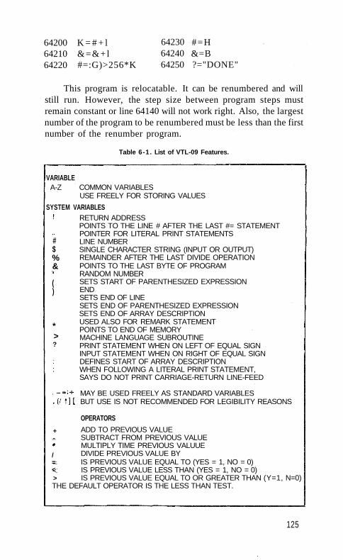
This program is relocatable. It can be renumbered and will still run. However, the step size between program steps must remain constant or line 64140 will not work right. Also, the largest number of the program to be renumbered must be less than the first number of the renumber program.
Table 6-1. List of VTL-09 Features.
VARIABLE A-Z COMMON VARIABLES
USE FREELY FOR STORING VALUES
SYSTEM VARIABLES RETURN ADDRESS POINTS TO THE LINE # AFTER THE LAST #= STATEMENT POINTER FOR LITERAL PRINT STATEMENTS LINE NUMBER SINGLE CHARACTER STRING (INPUT OR OUTPUT) REMAINDER AFTER THE LAST DIVIDE OPERATION POINTS TO THE LAST BYTE OF PROGRAM RANDOM NUMBER SETS START OF PARENTHESIZED EXPRESSION END SETS END OF LINE SETS END OF PARENTHESIZED EXPRESSION SETS END OF ARRAY DESCRIPTION USED ALSO FOR REMARK STATEMENT POINTS TO END OF MEMORY MACHINE LANGUAGE SUBROUTINE PRINT STATEMENT WHEN ON LEFT OF EQUAL SIGN INPUT STATEMENT WHEN ON RIGHT OF EQUAL SIGN DEFINES START OF ARRAY DESCRIPTION WHEN FOLLOWING A LITERAL PRINT STATEMENT, SAYS DO NOT PRINT CARRIAGE-RETURN LINE-FEED
MAY BE USED FREELY AS STANDARD VARIABLES BUT USE IS NOT RECOMMENDED FOR LEGIBILITY REASONS
OPERATORS
ADD TO PREVIOUS VALUE SUBTRACT FROM PREVIOUS VALUE MULTIPLY TIME PREVIOUS VALUUE DIVIDE PREVIOUS VALUE BY IS PREVIOUS VALUE EQUAL TO (YES = 1, NO = 0) IS PREVIOUS VALUE LESS THAN (YES = 1, NO = 0) IS PREVIOUS VALUE EQUAL TO OR GREATER THAN (Y=1, N=0)
THE DEFAULT OPERATOR IS THE LESS THAN TEST.
125
+ -* / = < >
64200 64210 64220
K = # + l &=&+l #=:G)>256*K
64230 64240 64250
#=H &=B ?="DONE"
* > ?
# $ % & ' ( )

Time of Day Digital Clock Programs FOR 300 BAUD TERMINALS
10 20 30 40 50 60 70 80 90 100 110 120 130 140
10 20 30 40 50 60
?="HOUR ?"; H=? ?="MINUTE ?"; M=? ?="SECOND ?"; S=? ?="READY" A=$ S=S+1
M=S/60+M S=% H=M/60+H M=% H=H/24*0+%
150 160 170 180 190 200 210 220 230 240 250 260 270 280 290
?="TIME: "; ?=H/10 ?=% ?=": "; ?=M/10 ?=%
?=": "; ?=S/10 ?=% $=13 A=B T=31 T = T - 1 #=T=0*90 #=270
FOR 110 BAUD TERMINALS ?="HOUR ?"; H=? ?="MINUTE ?"; M=? ?="SECOND ?"; S=?
70 80 90 100 110 120
?="READY" A=$ S=S+1 M=S/60+M S=% H=M/60+H
126
Hurkle Program 100 110 120 130 140 150 160 170 180 190 200 210 220 230 240 250 260 270 280 290 300 310 320 330
?="" ?="A HURKLE IS HIDING ON A" ?="10 BY 10 GRID. HOMEBASE" ?="ON THE GRID IS POINT 00" ?="AND A GRIDPOINT IS ANY" ?="PAIR OF WHOLE NUMBERS" ?="TRY TO GUESS THE HURKLE'S" ?="GRIDPOINT. YOU GET 5 GUESSES' ?="" R=7100*0+% A=R/10 8=% K=1 ?="GUESS#"; ?=K ?=" ?"; X=?/10 Y=%
?="" #=X*10+Y=R*540 K=K+1 #=K=6*440 ?="GO "; #=Y=B*370+(4<B*360)
340 350 360 370 380 390 400 410 420 430 440 450 460 470 480 490 500 510 520 530 540 550 560 570
?="SOUTH"; #=370 ?="NORTH"; #=X-A*410+(X<A*400) ?="WEST"; #=410 ?="EAST"; ?="" ?="" #=230 ?="" ?="SORRY THAT'S 5 GUESSES" ?="THE HURKLE IS AT "; ?=A ?=B ?="" ?="" ?="LETS PLAY AGAIN." ?="HURKLE IS HIDING" # = 1 8 0 ?="YOU FOUND HIM IN "; ?=K ?=" GUESSES" #=490
130 140 150 160 170 180 190 200 210
M=% H=H/24*0+% ?=H/10 ?=% ?=": "; ?=M/10 ?=%
?=": " ?=S/10
220 230 240 250 260 270 280 290 300 310
?=% $=13 A=B A=B A=B A=B+B T=14 T = T - 1 #=T=0*90 #=290
Factorials Program
This program calculates factorials until it runs out of memory. For 1K of memory, this is about 208!
10 20 30 40 50 60 70 80 90 ioo 110 120 130 140 150 160 170 180
A=l L=2 :1)=1 I=2 :I)=0 I=I+1 #=L>I*50 ?="" ?="" ?=A ? = " : = " ?="" I=L+1 I = I - 1 # = : I)=0*140 ?=: I) I = I - 1 #=I=0*220
190 200 210 220 230 240 250 260 270 280 290 300 310 320 330 340 350 360 370
?=:I)/10 ?=% #=170 A=A+1 I=1 C=0 X=:I) :I)=A*X # = : I)<X*320 : I)=: I)+C C=: I)/100 : l)=% I=I+1 #=L>I*250 #=C=0*80 L=L+1 #=*-&/2<L*380 : I )=C #=290
127
Weekday Program 10 20 30 40 50 60 70 80
#=440 ?="DAY OF THE WEEK" ?="" ?="MONTH? "; M=? #=M>13*40 #=M=0*40 ?="DAY OF MONTH? ";
90 100 110 120 130 140 150 160
D=? ?="YEAR? " Y=? #=Y>1800*230 #=Y<100*150 #=70 ?="" ?="IS THAT 19";
170 180 190 200 210 220 230 240 250 260 270 280 290 300 310 320 330 340 350 360
?=Y ?="? "; K=$ #=K=89=0*70 ?="ES" Y=Y+1900 C=Y/100 Y=% #=Y/4*0+% =0*280 : 1)=6 : 2)=2 N=Y/4+Y+D+:M)+(2*(C=18))/7*0+% #=300+(20*W) ?="SUN"; #=430 ?="MON"; #=430 ?="TUES"; #=430 ?="WEDNES";
370 380 390 400 410 420 430 440 450 460 470 480 490 500 510 520 530 540 550 560
#=340 ?="THURS"; #=430 ?="FRI"; #=430 ?="SATUR"; ?="DAY" :1)=0 :2)=3 :3)=3 :4)=6 :5)=1 :6)=4 :7)=6 :8)=2 :9)=5 :10)=0 :11)=3 :12)=5 #=20
Starshooter Program
10 20 30 40 50 60 70 80 90 100 110 120 130 HO 150 160 170 180 190 200
I=0 I=I+1 : I)=46 #=I<41*20 :25)=42 I=8 J = l $=I - /7+64
?" - "; S=I+J $=:S) J=J+1 #=J=6*160
?=" "; #=100 I=I+7 ?="" ?="" #=I<43*70 ?=""
210 220 230 240 250 260 270 280 290 300 310 320 330 340 350 360 370 380 390 400
?=" 1 2 3 4 5" ?="" ?="YOUR MOVE --"; I=42 I=I+1 : I )=$ # = : I)=13*320 # = : I)=3*580 # = : I)=95=0*250 I = I - 1 #=260 A=:43)-64 ?="" #=A>6*230 B=:44)-48 #=B>6*230 S=A*7+1+B ?="" #=:S)=42*420 ?="THAT'S NOT A STAR!"
128

410 420 430 440 450 460 470 480
#=230 :S)=46 C = S - 7 #=520 C = S - 1 #=520 C=S+1 #=520
490 500 510 520 530 540 550 560 570
C=S+7 #=520 #=60 =! # = : C)=42*560 :C)=42 # = :C)=46 # =
The object of the game is to change this:
129
Factors of a Number Program
This version is for the TVT: 10 20 30 40 50 60 70 80 90 100 110 130 140 150 160 170 180 190
#=200 D=D+2/3*0+%=0*2+(D>3)+D+l Q=N/D #=Q<D*300 #=%>1*20 ?="" ?=D N=Q Q=N/D
#=%>1*20 ?=" "; P=l N=Q Q=N/D P=P+1 #=% =0*140 ?=P #=20
200 210 220 230 240 250 260 270 280 300 310 320 330 340 350 360 370 380
?="NUMBER? "; N=? X=N $=22 ?=" " ?=N ?=" IS "; D=2 #=30 #=N=X*370 #=N=1*340 ?="" ?=N ?="" ?="DONE" #=200 ?="PRIME" #=200
Primes Program
This version is for the 32 Char Terminal: 10 #=100 30 D=D+2/3*0+%=0*2+(D>3)+D+l 20 #=D>Q*150 40 Q=N/D
50 #=%>1*20 60 70 80 90 100 101 102 104 106 110 115 120
N=N+2/3*0+%=0*2+(N>3)+N+l D=2 #=N<65533*40 #=N $=28 #=102 ?=" PRIMES" ?="" ?=" "; ?=1
?=" "; N=2
130 150 160 170 180 190 195 200 205 210 220 230 240 250
A=l B=N #=B>10000*200 $=32 #=B>1000*200 B*B*10 #=170 ?=N
?=""; A=A+1 #A<5*60 ?="" A=0 #=60
130
10 20 30 40 50 60 70 80 90 100
no 120 130 140 150 160 170 180 190 200 210 220 230 240 250 260 270 280 290 300
T=100 $=22 ?="CRAPS!" ? = " " ?="HOW MUCH DO YOU BET? - "; B=? #=B=0*90 ?="GOOD LUCK!" #=B=8*480 #=T>B*160 ?="TOO MUCH!" ?="YOU HAVE $"; ?=T ?=" LEFT. " #=40 ?="" ?="ROLL-"; A=? $=22 ?="FIRST ROLL: "; #=500 #=R=7*360 #=R11*360 #=R<4*390 #=R=12*390 ?="" ?=R ?=" IS YOUR POINT" P=R ?="ROLL-":
310 320 330 340 350 360 370 380 390 400 410 420 430 440 450 460 470 480 490 500 510 520 530 540 550 560 570 580 590 600 610
A=$ #=500 #=R=7*390 #=R=P*360 #=300 ?="YOU WIN" T=T+B #=120 T = T - B ?="YOU LOSE" #=T=0*430 #=120 ?="YOU ARE BUSTED!" ?="MOVE OVER AND LET THE NEXT" ?="SUCKER TRY." ? = " "
#=10 ?="BE SERIOUS" #=40 R='/6*0+% + l ?=R X=X+11213 ?=" AND "; S='/6*0+%+1 X=X*56001 ?=5 ?=" ("; R=R+S ?=R ?=")"
#=!
Craps! Program
Cipher Game Program
10 I=0 20 I=I+1 30 : - ) = I + 6 4
40 50 60
+=I<26*20
I=I ?=""
70 80 90
M='/26*0+%+l H=:M) : M)=: I)
100 110 120 130 140 150 160 170 180 190 200 210 220 230 240 250 260 270 280
: I)=H I=I+1 #=I<27*70 ?="TEXT?" ?="" I=27 : I)=$ #=: I)=13*220 #=: I)=95=0*200 I=I-2 I=I+1 #=160 ?="" I=27 #=: I)<64*270 T=: I)-64 : I)=T) I=I+1 #=: I)>14*240
290 300 310 320 330 340 350 360 370 380 390 400 410 420 430 440 450 460 470 480 490 500
?="" ?="CODE: " ?="" I=27 $=: 1) #=: I)=l3*370 I=I+1 #=330 ?="" ?="SWITCH? - "; A=$ B=$ #=B=64*370 I=27 #=: 1)=A*490 #=: I)=B=0*460 :I)=A I=I+1 #=: I)=13*290 #=430 : I)=B #=460
10 20 30 40 50 60 70 80 90
$=22 1=0 I=I+1 : I)=$ L=: I)=95*2 I=I- L #=: I)>14*30 ?="" I=1
100 110 120 130 140
K=I J=K #=:K)=32*160 #=:J)=32*150 #=:K)>: J)*160
150 160 170 180 190 200 210 220 230 240 250 260 270
J=K K=K+1 #=:K)>14*120 H=: I) : I)=: J) :J)=H I=I+1 #=: I)>14*100 I=0 I=I+1 $=:I) #=: I)>14*240 ?=""
Phrase Sort Program
131

Life (Fast Version) Program
10 20
25 30 40 50 70 80 90 100 110 120 130 140 150 160 180 190 200 210 220 230 240 250 260 270 280 290 300 310 320 330 340 350 360 370 380 390 400
#=370 S=Y<F*Y+(Y=0*E)+(Y=F)-1*0+(X<Q*X+(X=0*0)+(X=Q)) : S)=: S)+2 X=X+1-(J<X*3)+(J-1=X*(Y=I)) Y=J-1=X+Y #=I+1>Y*20 #=90 #=: I-l*O+J)/2*0+%*20 J=J+1-(O=J*O) I=J=I+I ?=""; X=J-1 Y=I-1 #=I<F*80 I=1 J=l ?="" P=0 K=I-1*O+J : K)=: K)<5+(: K)>8)=0 P=P+: K) $=: K)*10+32 J=J+1-(J=0*0) #=1<J*200 ?="" I=I+1 #=I<F*200 ?="GEN = "; ?=G G=G+1 ?=" POP = "; ?=P I=1 J=l #=0<P*110+(P=0*650) I=1 G=0 ?="SIZE? "; O=?
132

410 420 430 440 450 460 470 480 490 495 500 510 520 530 540 550 560 570 580 590 600 610 620 625 626 627 631 632 633 634 635 636 637 638 640
Q=O+1 ?="BY? "; E=? F=E+1 J=O*E+2 #=J*2+&>**390 : I)=0 I=I+1 #=J>I*470 #=631 I=1 ?="" J=l #=10*550 ?=""; ?=I ?=""; L=$ : I- l*O+J)=L=32+(L=13)+(L=95)+(L=64)=0*6 J=J+1-(L=95*2) #=L=13*620+(L=64*510) #=J<Q*570 I=I+1 #=I<F*510 #=631 #=150 $=22 $=18 $=32 $=18 $=22 $=18 $=32 $=18 $=!
This program takes at least 2 K of memory to operate satisfactorily.
133
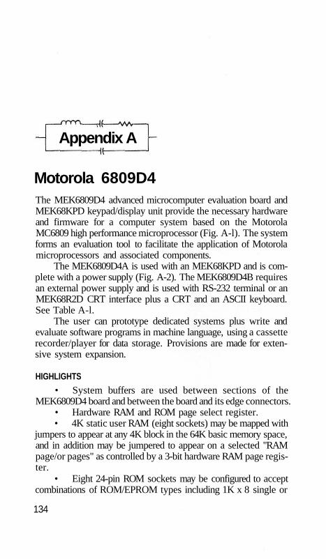
Appendix A
Motorola 6809D4 The MEK6809D4 advanced microcomputer evaluation board and MEK68KPD keypad/display unit provide the necessary hardware and firmware for a computer system based on the Motorola MC6809 high performance microprocessor (Fig. A-l). The system forms an evaluation tool to facilitate the application of Motorola microprocessors and associated components.
The MEK6809D4A is used with an MEK68KPD and is complete with a power supply (Fig. A-2). The MEK6809D4B requires an external power supply and is used with RS-232 terminal or an MEK68R2D CRT interface plus a CRT and an ASCII keyboard. See Table A-l.
The user can prototype dedicated systems plus write and evaluate software programs in machine language, using a cassette recorder/player for data storage. Provisions are made for extensive system expansion.
HIGHLIGHTS
• System buffers are used between sections of the MEK6809D4 board and between the board and its edge connectors.
• Hardware RAM and ROM page select register. • 4K static user RAM (eight sockets) may be mapped with
jumpers to appear at any 4K block in the 64K basic memory space, and in addition may be jumpered to appear on a selected "RAM page/or pages" as controlled by a 3-bit hardware RAM page register.
• Eight 24-pin ROM sockets may be configured to accept combinations of ROM/EPROM types including 1K x 8 single or
134

Fig. A-1. The MEK6809KPD keypad/display unit (courtesy of Motorola Semiconductor Products Inc.).
triple supply EPROMs or ROMs, 2K x 8 single or triple supply EPROMs or ROMs, 4K x 8 ROMs or EPROMs, or 8K x 8 ROMs or EPROMs.
• A ROM-based mapping technique is used to allow completely general address mapping of the eight ROM sockets anywhere in the 64K basic memory space with 1K resolution. In addition, the sockets may be mapped on any "ROM page/or pages" as controlled by a 3-bit hardware ROM page register.
• All memory and I/O on the board is fully decoded, so that address space not specifically required on the D4 is available for off-board mapping.
• A - 1 2 volt to - 5 volt regulator is provided to allow use of 3-supply EPROMs on the D4. Supply voltages of +12, - 1 2 , and +5 must be provided by the user.
• Hardware is provided which allows Monitor software to store and recover Kansas City Standard 300-baud or 1200-baud format cassette tape data.
• Interrupt driven stop-on-address comparator. • System clock derived from 3.579 MHz on-board XTAL or
from a 4 x TTL compatible external source. • "Test" signal and logic provided to allow control of on
board memory and I/O from an external processor through the 70-pin edge connector.
• Control and status lines provided for flexible hardware control of MPU and bus decode drive logic. This allows for: —Testing and debug -Interrupts (RESET, NMI, IRQ, FIRQ)
135

—Interrupt vectoring by device (IVE, STKOP) -Interrupt disable (IRQE, FIRQE) —Halt and bus request (BREQ) —Slow memory (MEMRDY) -DMA
The following features are standard on the MEK6809D4B and may be included as options on the MEK6809D4A: RS-232 compatible serial port including buffered handshake signals; baud rate generator providing baud rate clocks for 110, 300, 600, 1200, 4800, and 9600 baud rates; and address, data and control lines fully buffered at bus interface.
MODEL TYPES The MEK6909D4A has no RS-232 circuitry or address and
data buffers to the edge connector. The D4A is intended for use with the MEK68KPD keypad/display unit which has an on-board power supply to operate the system. No RAMs are provided in the "user RAM" array. A 4K monitor program is provided (Fig. A-3 and Table A-2).
The MEK6809D4B is intended for use with an RS-232 serial terminal or an MEK68R2D CRT interface as the system terminal. The D4B has RS-232 circuitry and data and address buffers.
To operate the RS-232 interface, the user must supply +12V, +5V, and -12 V power. A4K + 2K monitor is provided. No RAMs are provided in the "user RAM" array.
Fig. A-2. The basic MEK6809D4 advanced microcomputer evaluation board (courtesy of Motorola Semiconductor Products Inc.).
136
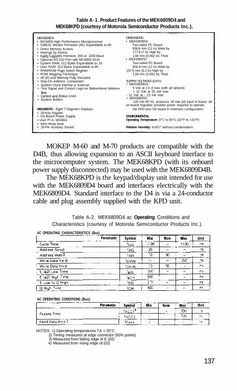
Table A-1. Product Features of the MEK6809D4 and MEK68KPD (courtesy of Motorola Semiconductor Products Inc.).
MEK6809D4 • MC6809 Hiqh Performance Microprocessor • D4BUG Monitor Firmware (4K) Expandable to 6K • Direct Memory Access • Interrupt by Device • Audio Cassette Interlace, 300 or 1200 Baud • Optional RS-232 Port with MC6850 ACIA • System RAM, 512 Bytes Expandable to 1K • User RAM. 512 Bytes Expandable to 4K • RAM/ROM Pago Select Register • ROM Mapping Technique • All I/O and Memory Fully Decoded • Stop-On-Address Comparator • System Clock Internal or External • Test Signal and Control Logic tor Bidirectional Address
Bus • Control and Status Lines • System Buffers
MEK68KPD- Eight 7-Segment Displays • 25-Key Keypad • On-Board Power Supply • User PI A, MC6821 • Wire-Wrap Area • 16-Pin Auxiliary Socket
DIMENSIONS • MEK6809D4:
Two-sided PC Board 309.8 mm (12 in) Wide by 177.8 (7 in) High by 1.59 mm (0.062 in) Thick
• MEK68KPD: Two-sided PC Board 304.8 mm (12 in) Wide by
157.5 mm (6.2 in) High by 1.59 mm (0.062 in) Thick
SUPPW VOLTAGES (£5%) • MEK6809D4:
5 Vdc at 2.0 A max (with all options) + 12 Vdc at 25 mA max
- 12 Vdc at - 23 mA max • MEK68KPD:
120 Vac 60 Hz, produces 18 Vac (ct) input to board. An on-board regulator provides power required to operate
the KPD plus D4 board in minimum configuration.
ENVIRONMENTAL Operating Temperature: 0°C to 55°C (32°F to 131°F)
Relative Humidity: to 8 0 * without condensation.
MOKEP M-60 and M-70 products are compatible with the D4B, thus allowing expansion to an ASCII keyboard interface to the microcomputer system. The MEK68KPD (with its onboard power supply disconnected) may be used with the MEK6809D4B.
The MEK68KPD is the keypad/display unit intended for use with the MEK6809D4 board and interfaces electrically with the MEK6809D4. Standard interface to the D4 is via a 24-conductor cable and plug assembly supplied with the KPD unit.
Table A-2. MEK6809D4 ac Operating Conditions and Characteristics (courtesy of Motorola Semiconductor Products Inc.).
AC OPERATING CHARACTERISTICS (Bus)
NOTES: 1) Operating temperatures TA = 25°C 2) Timing measured at edge connector (50% points) 3) Measured from falling edge of E (02) 4) Measured from rising edge of (02)
137
AC OPERATING CONDITIONS (Bus)

Fig. A-3. MEK6809D4 timing diagram (courtesy of Motorola Semiconductor Products Inc.).
EXPANSION
With the rapid advancements in the microprocessor industry, there is vital need to provide educational and evaluation material to help engineering/technical personnel stay abreast of this technology.
In response to this need Motorola Memory Systems has evolved a series of kit boards intended for the educational evaluation of the MC6800 family of integrated circuits. The series is called "MOKEP" (for Motorola Kit Expansion Products) and includes the following wide range of boards.
MEK68CC Card Cage. The MEK68CC is used with the MEK68MB5 motherboard.
MEK68MB5 Motherboard Module. The MEK68MB5 motherboard module has provisions for 10 card slots on " centers, with alternate slots populated with 70-Pin connectors.
MEK68CMB Card Cage/Motherboard. The MEK68CMB can accommodate ten cards of the MOKEP series. The card cage is identical to the MEK68CC. The motherboard is a fully populated version of the MEK68MB5 without the stand-alone card guides. The completed assembly measures 8-¼" high by 7-¼" wide by 13¼" deep.
MEK68R2/R2D/R2M Programmable CRT Interface Modules. The MEK68R2/R2D/R2M programmable CRT inter-
138

face modules are used in conjunction with other products in the MOKEP family to form a microcomputer system. The MEK68R2D is to be used with the MEK6809D4 microcomputer module and an MEK68MB series motherboard. All units feature software programmable line and character format, upper and lower case 5x7 matrix display, semigraphics, and up to 4K of screen display memory. All modules provide an interface for an ASCII keyboard.
MEK6810 Input/Output Module. The MEK6810 is supplied with a 300/1200 baud cassette interface, two MC6850 A CIAs, an MC14411 baud rate generator and one MC6821 PIA.
MEK68EP EPROM Programmer Module. The MEK68EP has provisions for programming both single and triple power supply types of 1K, 2K and 4K EPROMs.
MEK68RR ROM/RAM Module. The MEK68RR has provisions for eight ROM sockets which may be configured to accept 1K, 2K 4K or 8K single or triple supply ROMs or EPROMs. The board also has sockets for up to 8K bytes of static RAM.
MEK68MM16/MM32 16K/32K Memory Modules. The MEK68MM16 has 16K bytes of RAM and the MEK68MM32 has 32K bytes. The MEK68MM boards employ 16K dynamic RAMs and a hidden refresh technique to achieve the low cost, low power consumption and high density of dynamic memory systems, while appearing as static memory to the system. The MEK68MM fully supports the RAM paging technique of the D4 microcomputer module, allowing up to eight boards or 256K bytes of RAM to be used in one system.
MEK6809A Editor /Assembler . The MEK6809EA editor/assembler provides the user of the MEK6809D4B with the ability to enter, assemble, edit and save assembly language programs for execution on the M6809. The editor may also be used to enter and edit text files that will not be assembled for execution. The assembler will accept both M6800 and M6809 mnemonics. The object code from the assembler can be placed in memory or saved on tape. The MEK68R2D display and stand alone terminals are supported by software.
MEK68WW/WW1 Wirewrap Modules. The MEK68WW is used with the MEK6800AD adapter motherboard, and interfaces directly with the 60-Pin bus of the AB. The MEK68 WW1 utilizes a 70-pin bus, directly interfacing with the MEK68MB series motherboards. Either product can be used as a card extender. Both are supplied with components required for buffering of address, data and control buses.
139

SOFTWARE FEATURES
• Memory change display • Register change/display • Breakpoint editor • 4K monitor in position independent code (6K for
MEK6809D4B version) • Trace single step and user line • Go to user program • Calculate offset • Cassette punch/load/verify • Stop on address • Escape from all functions • 16 User special functions • Additional features on D48 include memory dump to
examine blocks of data, memory fill, memory search, memory move and ASCII entry
The MEK6809D4 operating system allows the development and operation of user-defined programs. The basic monitor program interfaces with an MEK68KPD keypad/display unit and is contained in a 4K byte ROM (MCM68332 or equivalent). This ROM is factory installed in all versions of the MEK6809D4 assembled units.
A second 2K byte ROM (MCM68316E or equivalent) is used with an MEK68R2D CRT monitor/ASCII keyboard interface or RS-232 compatible terminal. This additional 2K ROM is provided in the.MEK6809D4B version.
The monitor program source listings, complete with comments, are available from Motorola. The monitor program is written in highly subroutined, position independent code. These source listings provide a valuable starting point for many types of user programs.
The monitor program provides the following functions.
Examine/Change Memory Location This allows the user to open any memory location and display
the contents. New data may then be entered if desired, assuming read/write memory is present at the selected location. If an attempt is made to write into an invalid location, the new data will be displayed together with the fixed data at the invalid location. Only the new data is displayed when a valid change of read/write memory is accomplished. After the examine/change step, the user has
1 4 0

t h e o p t i o n o f a u t o m a t i c a l l y o p e n i n g e i t h e r t h e n e x t o r p r e v i o u s
l o c a t i o n — o r e s c a p i n g t o t h e m o n i t o r p r o g r a m .
E x a m i n e — C h a n g e R e g i s t e r s
T h i s f u n c t i o n a l l o w s t h e u s e r t o e x a m i n e / c h a n g e t w o e x t e r n a l
r e g i s t e r s p l u s t h o s e a r e a s o f t h e s t a c k R A M c o r r e s p o n d i n g t o t h e
s t o r a g e l o c a t i o n s o f t h e n i n e i n t e r n a l r e g i s t e r s o f t h e M C 6 8 0 9 . T h i s
h a s t h e e f f e c t o f a l l o w i n g t h e u s e r t o e x a m i n e / c h a n g e t h e s e r e g i s
t e r s .
T h i s f u n c t i o n d i f f e r s f r o m m e m o r y e x a m i n e / c h a n g e i n t h a t t h e
r e g i s t e r s a r e d i s p l a y e d i n a s e t s e q u e n c e . R e g i s t e r d e s i g n a t i o n a s
w e l l a s c o n t e n t s a r e d i s p l a y e d t o f a c i l i t a t e u s e o f t h e f u n c t i o n . T h e
t w o e x t e r n a l r e g i s t e r s a r e i n c o r p o r a t e d o n t h e M E K 6 8 0 9 D 4 t o
p e r f o r m o p e r a t i o n s n o t i n h e r e n t w i t h t h e M C 6 8 Q 9 .
S t o p o n A d d r e s s
I n d e - b u g g i n g p r o g r a m s , i t i s o f t e n a d v a n t a g e o u s t o b e a b l e t o
h a l t t h e m a c h i n e w h e n a s p e c i f i c a d d r e s s i s e n c o u n t e r e d . A t y p i c a l
e x a m p l e o f t h e u s e o f t h i s f u n c t i o n i s t o d e t e r m i n e t h e r e a s o n f o r a n
i n a d v e r t e n t ( o r i n c o r r e c t ) c h a n g e o f a m e m o r y l o c a t i o n d u r i n g t h e
r u n n i n g o f a U s e r p r o g r a m .
T h e s t o p o n a d d r e s s f u n c t i o n ( S O A ) f u n c t i o n i s i m p l e m e n t e d
o n t h e M E K 6 8 0 9 D 4 b y c i r c u i t r y w h i c h c o m p a r e s t h e M P U a d d r e s s
o u t p u t s w i t h u s e r - e n t e r e d d a t a i n t h e s t o p o n a d d r e s s r e g i s t e r .
P r o v i d i n g t h e S O A f u n c t i o n i s a r m e d , a n o n - m a s k a b l e i n t e r r u p t i s
g e n e r a t e d w h e n a c o m p a r i s o n i s a c h i e v e d .
D e p e n d i n g o n t h e t y p e o f i n s t r u c t i o n ( m o r e s p e c i f i c a l l y , u p o n
t h e t i m i n g r e l a t i o n s h i p o f t h e a d d r e s s a s s e r t i o n i n t h e i n s t r u c t i o n
c y c l e s ) , t h e N M I m a y b e r e c o g n i z e d a t t h e e n d o f t h e p r e v i o u s
i n s t r u c t i o n . C o n t r o l t h e n p a s s e s t o t h e m o n i t o r , a l l o w i n g t h e u s e r
t o d e t e r m i n e t h a t o n e o f t w o s p e c i f i c i n s t r u c t i o n s h a s a c c e s s e d t h e
s p e c i f i e d m e m o r y l o c a t i o n .
I n s o m e i n s t a n c e s i t i s d e s i r a b l e t o a l l o w t h e p r o g r a m t o s t o p
o n l y o n t h e N t h t i m e a n a d d r e s s i s e n c o u n t e r e d . T h e M E K 6 8 0 9 D 4
c a n i m p l e m e n t t h i s f u n c t i o n . I t i s a l s o p o s s i b l e t o o u t p u t a t r i g g e r
p u l s e e a c h t i m e t h e a d d r e s s i s e n c o u n t e r e d , r a t h e r t h a n s t o p p i n g
p r o g r a m e x e c u t i o n .
B r e a k p o i n t s
T h e S O A f u n c t i o n i s i m p l e m e n t e d i n h a r d w a r e . S o f t w a r e
m e t h o d s o f p r o g r a m e x e c u t i o n i n t e r r u p t i o n s i n c l u d e t h e s e t t i n g o f
1 4 1

breakpoints at desired locations in the program. This effectively substitutes a software interrupt for the instruction at that location.
Up to eight breakpoints can be set in the user program (provided the program is in RAM). As with SOA, the user has the option of allowing N-l breakpoints to be bypassed if desired. (The maximum value of N for either SOA or breakpoints is 255). The User can set, clear or examine breakpoints via the breakpoint editor function.
Trace Instruction
This function allows the User to step through a program one instruction at a time. At the end of each instruction, the examine/ change register routine is automatically entered, and the new program counter value is displayed.
Trace Line It is often desirable to trace through a program while treating a
subroutine as a single instruction. One obvious example of this is the situation wherein all subroutines have previously been thoroughly de-bugged. The MEK6809D4 debug routines allow this to be accomplished in either of two ways.
One of these (software method) involves a comparison of each instruction in a subroutine until the instruction following the subroutine is encountered. Thus, the portion of the program from a subroutine call to its return is treated as one instruction as far as the trace function is concerned. Nested subroutines are automatically handled by the monitor program.
The second trace line option uses the SOA circuitry. This has an advantage over the software method in that subroutine execution is in real time. This is particularly helpful in de-bugging time-dependent I/O routines. (It is also desirable for long subroutines, since the software method greatly increases the run time of a subroutine). Its disadvantage is that program execution often continues for one instruction after the return.
User Program Control
The MEK6809D4 de-bug routines include functions to allow the user to go to, continue, or abort user programs.
Offset Calculation In generation or modification of programs, it is often neces
sary to calculate the offset from the location of a jump or branch
1 4 2

instruction to its destination. Some indexed mode instructions also use relative offsets. The examine/change memory location includes a subfunction to allow this to be easily accomplished.
The user opens the location of the offset, types the offset command, then enters the desired destination address. The MEK6809D4 calculates the required offset, displays it, and enters the data in the appropriate memory location(s). The offset calculation supports both short and long offsets.
Punch/Load/Verify Audio Cassette
The audio cassette interface is a modified Kansas City Standard version capable of operation at either 300 or 1200 baud. The interface allows any of the three functions (punch, load or verify with memory) to operate with or without an optional offset. This is particularly useful for user programs written in position independent code.
ADDED D4B SOFTWARE FEATURES
The memory dump command allows the user to display blocks of memory with ASCII equivalents. The display for mats differ slightly depending on the display device configuration. The ending address must be a larger hexadecimal number than the beginning address or a warning will be issued, followed by a new request for a begin address. The dump command cannot proceed until a satisfactorily address range has been specified.
Memory fill allows the user to fill a block of memory with a four byte pattern. The beginning and ending addresses are entered as in the memory dump command.
Memory search allows search of a specified block of memory for a 4 byte pattern subject to a corresponding 4 byte mask. For all bits in the mask which are zero, the corresponding bit in the pattern is considered to be "don't care."
After the mask has been specified, the search function will be performed over the specified address range. Each time the comparison alogrithm is successful, the address of the first location of the match is displayed. If the list of successful addresses is being displayed too quickly, the listing may be temporarily halted by typing (ESCAPE) as in the memory dump command.
Memory Move allows the user to move a block of data from one area in memory to a new area. The beginning and ending addresses are entered the same way as in memory dump. Following entry of
1 4 3

the end address, a message will appear requesting entry of the new beginning address where the block of data is to be moved.
ASCII Entry allows a user to store ASCII data to memory quickly and easily without having to look up each ASCII character to determine its hexadecimal equivalent. Features are incorporated to assist in setting up messages for the D4BUG callable subroutine "PDATA."
MEK6809D4 DESCRIPTION
The CPU consists of an MC6809 high performance micro-procesor, a 3.579 HMz crystal, and buffers which interface the MC6809 to other circuit blocks on the D4 board.
The MC6809 supports programming techniques such as position independence, re-entrancy and modular programming. The MC6809 has hardware and software features which make it a suitable processor for higher level language execution or standard controller application (Fig. A-4).
Rom
The ROM system consists of eight ROM sockets which may be configured to accept various combinations of ROM types. These include single or triple power supply varieties of 1K, 2K, 4K, or 8K x 8 ROMs or EPROMs. The ROM type configurations are controlled by mini-jumpers which may be easily moved without the need for any tools.
Mapping of the eight ROMs in memory space is accomplished by a mapping ROM which is used as a programmed logic array. A paging technique allows up to 192K bytes of ROM to be used in the D4 system.
Ram
There are two groups of 1K x 4 RAMs. One group is the stack RAM and the other is the user RAM,
The stack RAM is used mainly for the D4 operating system stack and scratch RAM. Also, 512 bytes are available for user RAM application. This RAM is always located in the D4 system at memory location $E400 through $E7FF. The user RAM is a 4K x 8 block of memory that can be positioned anywhere in the D4 memory map, using jumper connections.
It is possible to disable the eight user RAM sockets to allow use of a MOKEP MEK68MM memory board for system expansion.
144

CPU
Y2
MC6809 MPU U39
16
MA0-MA15
ROM PROGRAM ROM C U47
ADDRESS BUFFERS U57. U58
BDG-BD7
ADDRESS
ADDRESS DECODE &
BUFFER CONTROLS
SELECT LINES BUFFER CONTROLS
STOP-ON-ADDRESS
BDO-
BD7
XTAL
BAUD RATE
GENERATOR U1
LEVEL TRANSLATORS
U2. 10
INPUT POWER
CONTROL & STATES BUFFERS U49. 5 1 . 52. 53. 54. 55 MEK68 KPD
(KEYPAID DISPLAY) R8232 TERMINAL
(CRT KEYBOARD]
M-7Q BUS (EDGE CONN) INPUT POWER -CONTROL & STATUS BUFFERS
U49, 51, 52, 53, 54, 55
Fig. A-4, MEK6809D4 block diagram (courtesy of Motorola Semiconductor Products Inc.).
MD0-MD7
ADDRESS BUFFERS U42. U 4 3 .
BD0-BD7 16 BA0-BA15
DATA U41
BA0-BA15
DATA
BA0-BA16 16 BD0-BD7
DATA U56
D0-D7 A0-A15 161 8
16
DATA U28
IDQ-ID-7 ID0-ID7
BDO-BD" BA0-BA15
ROM
D
U48
MONITOR
ROM
A
U45
ROM
B
U46
USER
ROM
E
U59
ROM
F
U60
ROM
G
U61
16 BAQ-BA15
RD0-RD7
ROM
H
U62 DATA U29
ID0-ID7 16
EAR CASSETTE INTERFACE
U5 MIC
STOP PIA U 4 U13
U12
U11
U14
RAM USER STACK
U18 U19 U20 U21 U17
RAM D RAM C RAM B RAM A
U34 U35 U36 U37 U33
ID0-ID7
BA0-BA15
BAC-
BA15
KPD CONNECTOR
AUX CONNECTOR
16 24
CONN CONN OPTIONAL
CONN
ACIA U3
R8232
Y1
R8232 CONNECTOR
COMPARATORS
145

Another jumper, when removed, prevents the user RAM from being written into (write protect), but the stack RAM is not affected. With the jumper in place, read and write to the user RAM is normal.
Address Bus System In some microprocessor systems, the address flow is from the
microprocessor through buffers and to the motherboard bus. The D4 uses a more complex arrangement that permits disabling the microprocessor. This allows addresses to be fed to the D4 from an external source, to access board components and permits DMA (direct memory access) for some applications.
The Data Bus System
There are four bi-directional data buffers used in the D4; a ROM buffer, RAM/IO buffer, edge buffer, and MPU buffer. Each buffer has an enable and a direction input. Control logic configures these buffers to route data between sections of the D4 board.
The Stop-On-Address Circuit
The purpose of a stop address is to enable a user program to be executed until a certain address is reached. The address to be stopped on is stored and when the board address bus bits coincide, an output results. This causes a nonmaskable interrupt to occur which switches the microprocesor to a service routine.
When a coincidence of address occurs, an NMI is not necessarily generated. In these cases, the comparator output is available at a test point to provide a trigger signal to an oscilloscope.
The RS-232 Circuit
The RS-232 specification defines a standard for interconnecting computer terminals of different makes. The ACIA converts the parallel data on the buses to serial data. The serial data is then translated into RS-232 levels.
The Cassette Circuit Interface
The D4 uses very few components to interface a tape recorder to its operating system. Most of the cassette operation occurs in software, to create tapes and recover data from tapes. The tape information consists of a stream of 1200 and 2400 Hz serial audio data.
146
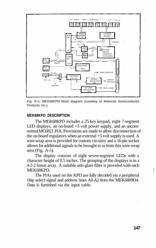
DISPLAYS
120 VAC
+5 (OPTION!
Fig. A-5. MEK68KPD block diagram (courtesy of Motorola Semiconductor Products Inc.).
MEK68KPD DESCRIPTION The MEK68KPD includes a 25-key keypad, eight 7-segment
LED displays, an on-board +5 volt power supply, and an uncommitted MC6821 PIA. Provisions are made to allow disconnection of the on-board regulators when an external +5 volt supply is used. A wire-wrap area is provided for custom circuitry and a 16-pin socket allows for additional signals to be brought to or from this wire-wrap area (Fig. A-5).
The display consists of eight seven-segment LEDs with a character height of 0.5 inches. The grouping of the displays is in a 4-2-2 linear array. A suitable anti-glare filter is provided with each MEK68KPD.
The PIAs used on the KPD are fully decoded via a peripheral chip select signal and address lines A0-A2 from the MEK6809D4. Data is furnished via the input cable.
147
KEYPAD MATRIX 6-ROWS BY 4-COLUMNS
MUX U13
4-COL
KEY
U14
RS
6-ROWS
CATHODE DRIVERS
U11, 13, 15, 16
ANODE DRIVERS 01-06 _
KPD PIA
6 7
LEDi Ui
LED U2
LED U3
LED U4
LED U5
LED U6
LED U7
LED U8
KPD CONN
ID0-ID7
USER PIA
U10
AUX CONN
XFMR 18 VAC
RECTIFIER CR1.CR2
J1
+5V LOGIC REGULATOR
VR1
DRIVE LOGIC
DISPLAY BUFFERS
+ 5V DISP. REGULATOR
VR2
DRIVE DISPLAYS
WIRE-WRAP
AREA
U9
J2
2
20

O R I G I N A L W H I T E

Appendix B
Hexadecimal Values of Machine Codes
OP Mown
113F SWI/3
1183 CMPU
118C CMPS
1193 CMPU
Mode
Inherent
immed
immed
Direct
~
20
5
5
7
#
2
4
4
3
NOTE All unused opcodes are both undefined and illegal
OP Mnem
119C CMPS
11A3 CMPU
11AC CMPS
11B3 CMPU
11BC CMPS
Mode
Direct
Indexed
Indexed
Extended
Extended
~
7
7 +
7 +
8
8
#
3
3 +
3 +
4
4
Coui'leBy of American Microsystems, Inc.
149

150 OP Mnem
00 NEG
01 •
02 •
03 COM
04 LSR
05 •
06 ROR
07 ASR
08 ASL/LSL
09 ROL
OA DEC
OB •
OC INC
OD TST
OE JMP
OF CLR
10 Page 2
11 Page 3
12 NOP
13 SYNC
14 •
15 •
16 LBRA
17 LBSR
18 •
19 DAA
Mode
Direct
Direct
— —
Inherent
Inherent
Relative
Relative
~
6
6
6
6
6
6
6
6
6
6
3
6
—
—
2
2
5
9
2
#
2
2
2
2
2
2
2
2
2
2
2
2
—
—
1
1
3
3
1
OP Mnem
30 LEAX
31 LEAY
32 LEAS
33 LEAU
34 PSHS
35 PULS
36 PSHU
37 PULLI
38 •
39 RTS
3A ABX
3B RTI
3C CWAI
3D MUL
3E •
3F SWI
40 NEGA
41 •
42 •
43 COMA
44 LSRA
45 •
46 RORA
47 ASRA
48 ASLA/LSLA
49 ROLA
Mode
Indexed
indexed
Inherent
Inherent
Inherent
~
4 +
4 +
4 +
4 +
5 +
5 +
5 +
5 +
5
3
6/15
20
11
19
2
2
2
2
2
2
2
#
2 +
2 +
2 +
2 +
2
2
2
2
1
1
1
2
1
1
1
1
1
1
1
1
1
OP Mnem
60 NEG
61 •
62 •
63 COM
64 LSR
65 •
66 ROR
67 ASR
68 ASL/LSL
69 ROL
6A DEC
6B •
6C INC
60 TST
6E JMP
6F CLR
70 NEG
71 •
72 •
73 COM
74 LSR
75 •
76 ROR
77 ASR
78 ASL/LSL
79 ROL
Mode
Indexed
Indexed
Extended
A
~
6+
6+
6+
6+
6+
6+
6+
6+
6+
6+
3 +
6+
7
7
7
7
7
7
7
#
2+
2+
2+
2+
2+
2+
2+
2+
2+
2+
2+
2+
3
3
3
3
3
3
3

1A ORCC
IB •
1C ANDCC
1D SEX
1E EXG
1F TFR
20 BRA
21 BRN
22 BHI
23 BLS
24 BHS/BCC
25 BLO/BCS
26 BNI
i 27 BEQ
i 28 BVC
29 BVS
2A BPL
2B BM
2C BGE
20 BIT
2E BGT
2F BLE
Immed
Immed
Inherent
Inherent
Relative
Relative
3
3
2
8
6
3
3
3
3
3
3
3
3 3
3
3
3
3
3
3
3
2
2
1
2
2
2
2
2
2
2 2
2
2
2
2
2
2
2
2
2
2
NOTE: All unused opcodes are both undefined and ilegal
4A DECA
4B •
4C INCA
4D TSTA
4E •
4F CLRA
50 NEGB
51 •
52 •
53 COMB
54 LSRB
55 •
56 •
56 RORB
57 ASRA
58 ASLB/LSLB
59 ROLB
5A DECB
58 •
5C INCB
50 TSTB
5E •
5F CLRB
Inherent
Inherent
Inherent
2
2
2
2
2
2
2
2
2
2
2
2
2
2
2
1
1
1
1
. 1
1
1
1
1
1
1
1
1
1
1
7A DEC
7B •
7C INC
7D TST
7E JMP
7F CLR
80 SUBA
81 CMPA
82 SBCA
83 SUBD
84 ANDA
85 BITA
86 LDA
87 •
88 EORA
89 ADCA
8A ORA
8B ADDA
8C CMPX
80 BSR
8E LDX
8F •
Extended
Immed
Immed
Relative
Immed
7
7
7
4
7
2
2
2
4
2
2
2
2
2
2
2
4
7
3
3
3
3
3
3
2
2
2
3
2
2
2
2
2
2
2
3
2
3
Legend
~ Number of MPU cycles (less possible push/pull or indexed-mode cycles)
# Number of program bytes
* Denotes unused opcode
151

OP Mnem
90 SUBA
91 CMPA
92 SBCA
93 SUBD
94 ANDA
95 BITA
96 LDA
97 STA
98 EORA
99 ADCA
9A ORA
9B ADDA
9C CMPX
9D JSR
9E LDX
9F STX
A0 SUBA
A1 CMPA
A2 SBCA
A3 SUBD
A4 ANDA
A5 BITA
A6 LDA
A7 STA
A8 EORA
A9 ADCA
Mode
Dir
Direct
Indexed
~
4
4
4
6
4
4
4
4
4
4
4
4
6
7
5
5
4+
4+
4+
6+
4+
4+
4+
4+
4+
4+
#
2
2
2
2
2
2
2
2
2
2
2
2
2
2
2
2
2+
2+
2+
2+
2+
2+
2+
2+
2+
2+
OP Mnem
C3 ADDD
C4 ANDB
C5 BITB
C6 LDB
C7 •
C8 EORQ
C9 ADCB
CA ORB
CB ADDB
CC LDD
CD •
CE LDU)
CF •
D0 SUBB
D1 CMPB
D2 SBCB
D3 ADDD
D4 ANDB
D5 BITB
D6 LDB
D7 STB
D8 EORB
D9 ADCB
DA ORB
DB ADDB
DC LDD
Mode
Immed
Immed
~
4
2
2
2
2
2
2
2
3
3
4
4
4
6
4
4
4
4
4
4
4
4
5
#
3
2
2 2
2
2
2
2
3
3
2
2
2
2
2
2
2
2
2
2
2
2
2
OP Mnem
F6 LDB
F7 STB
F8 EORB
F9 ADCB
FA ORB
FB ADDB
FC LDD
FD STD
FE LDU
FF STU
1021 LBRN
1022 LBHI
1023 LBLS
1024 LBHS/LBCC
1025 LBCS/LBLO
1026 LBNE
1027 LBEQ
1028 LBVC
1029 LBVS
102A LBPL
102B LBMI
Mode
Extended
Extended
Relative
~
5
5
5
5
5
5
6
6
6
6
5
5(6)
5(6)
5(6)
5(6)
5(6)
5(6)
5(6)
5(6)
5(6)
5(6!
#
3
3
3
3
3
3
3
3
3
3
4
4
4
4
4
4
4
4
4
4
4
152

AA
AB
AC
AD
AE
AF
B0
B1
B2
B3
B4
B5
B6
B7
B8
B9
BA
BB
BC
BC
BE
BF
C0
C1
C2
ORA
ADDA
CMPX
JSR
LDX
STX
SUBA
CMPA
SBCA
SUBD
ANDA
BITA
LDA
STA
EORA
ADCA
ORA
ADDA
CMPX
JSR
LDX
SFX
SUBB
CMPB
SBCB
4+
4+
6+
7+
5+
5+
5
5
5
7
5
5
5
5
5
5
5
5
7
8
6
6
2
2
2
2+
2+
2+
2+
2+
2+
3
3
3
3
3
3
3
3
3
3
3
3
3
3
3
3
2
2
2
Immed
NOTE: All unused opcodes are both undefined and illegal
DD
DE
DF
E0
E1
E2
E3
E4
E5
E6
E7
E8
E9
EA
EB
EC
ED
EE
EF
F0
F1
F2
F3
F4
F5
STD
LDU
STU
SUBB
CMPB
SBCB
ADDD
ANDB
BITB
LDB
STB
EORB
ADCB
ORB
ADDB
LDD
STD
LOU
STU
SUBB
CMPB
SBCB
ADDC
ANDE
BITB
102C
102D
102E
102F
103F
1083
108C
108E
1093
109C
109E
109F
10A3
10AC
10AE
10AF
1083
10BC
10BE
10BF
10CE
10DE
10DF
10EE
10EF
10FE
10FF
LBGE
LBLT
LBGT
LBLE
SWI/2
CMPD
CMPY
LDY
CMPD
CMPY
LDY
STY
CMPD
CMPY
LDY
STY
CMPD
CMPY
LDY
STY
LDS
LDS
STS
LDS
STS
LDS
STS
153
Indexed
Extended
Extended
Immed
5
5
5
1+
4+
4+
6+
4+
4+
4+
4+
4+
4+
4+
4+
5+
5+
5+
5+
b
5
5
7
5
5
2
2
2
2+
2+
2+
2+
2+
2+
2+
2+
2+
2+
2+
2+
2+
2+
2+
2+
3
3
3
3
3
3
5(6)
5(6)
5(6)
5(6)
20
5
5
4
7
7
6
6
7+
7+
6+
6+
8
8
7
7
4
5
6
6+
6+
7
7
3+
3+
3+
3+
4
4
4
4
4
3
3
3+
3+
4
4
Relative
Relative
Relative
Inherent
Immed
Immed
Direct
Direct
Indexed
Indexed
Extended
Extended
immed
Direct
Direct
indexed
Indexed
Extended
Extended
Direct
Indexed
Indexed
Extended
Extended
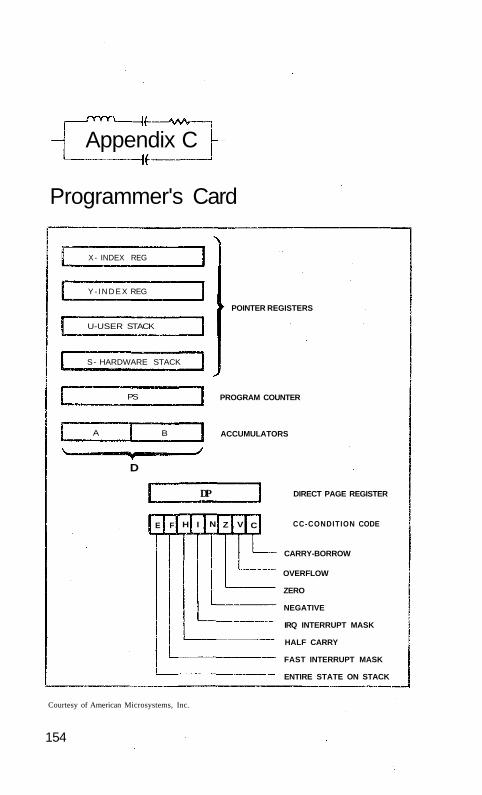
Appendix C
Programmer's Card
POINTER REGISTERS
PROGRAM COUNTER
ACCUMULATORS
DP DIRECT PAGE REGISTER
CC-CONDITION CODE
CARRY-BORROW
OVERFLOW
ZERO
NEGATIVE
IRQ INTERRUPT MASK
HALF CARRY
FAST INTERRUPT MASK
ENTIRE STATE ON STACK
Courtesy of American Microsystems, Inc.
154
X- INDEX REG
Y - I N D E X REG
U-USER STACK
S- HARDWARE STACK
PS
A B
D
E F H I N Z V C

HOW TO USE THE TABLES
CONVERSION TO DECIMAL: Find the decimal weighls For cor
responding hexadecimal characters beginning with the least
significant character. The sum of the decimal weight is the
decimal value of the hexadecimal number.
CONVERSION TO HEXADECIMAL: Find the highest decimal
value in the table which is lower than or equal to the decimal
number to be converted. The corresponding hexadecimal
character is the most significant character. Subtract the
decimal value found from the decimal number to be converted.
With the difference. repeat the process to find subsequent
hexadecimal characters.
HEXADECIMAL AND DECIMAL CONVERSION
15
1 5
HEX
0
1
2
3 4
5
6
7
8
9 A
B
C
D
E
F
CHAR
4
8
12
16
20
24
28
32
36
40
45
49
53
57
61
BYTE
12
DEC
0
096
192
288
384
480
576
672
768 864
960
056
152
248
344
440
1 1
HEX
0
1
2
3 4
5
6
7
8
9 A
B
C
D
E
F
CHAR
1
1
1
1
2
2
2
2
3
3
3
3
8
8
DEC
0
256
512
768 024
280
536
792
048 304
560
816
072
328 584
840
7
7
HEX
0
1
2
3 4
5
6
7
8
9 A
B
C
0
E
F
BYTE
CHAR 4
DEC
0
16
32
48 64
80
96
112
128
144
160
176
192
208 224
240
3 CHAR
HEX
0
1
2
3
4
5
6
7
8
9
A
B
C
0
E
F
0
0
DEC
0
1
2
3
4
5
6
7
8
9
10
11
12
13
14
15
POWERS OF TWO
2n
1
2 4
8
16
32
64
128
256
512
1.024
2.048
4.096
8.192
16.384
32.768
65.536
131.072 262.144
524.288
1.048.576
n
1
2
3
3
4
5
6
7
8
9
10
11
12
13 14
15
16
17
18
19
20
155
INCREASING MEMORY
HEXADECIMAL AND DECIMAL CONVERSION
6 8 0 9 STACKING ORDER SIMPLE CONDITIONAL BRANCHES
P U L L O R D E R
PUSH ORDER
CC
A
B
DP
X Hi
X Lo
Y Hi
Y Lo
U/S Hi
U /S Lo
PC Hi
PC Lo
FFFE FFFC FFFA FFF8 FFF6 FFF4 FFF2 FFF0
6809 VECTORS RESTART NMI SWI IRQ FIRQ SWI2 SWI3 RESERVED
Condition
BEQ
BMI
BCS
BVS
Complement
BNE
BPL
BCC
BVC
Condition
BGT
BGE
BEQ
BLE
BLT
Complement
BLE
BLT
BNE
BGT
BGE
Condition
BHI
BHS
BEQ
BLS
BLO
Complement
BLS
BLO
BNE
BHI
BHS
UNSIGNED CONDITIONAL BRANCHES
SIGNED CONDITIONAL BRANCHES
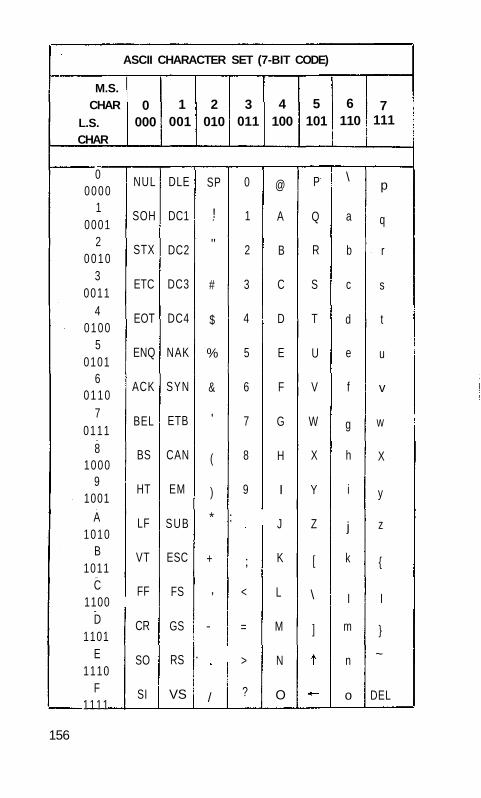
ASCII CHARACTER SET (7-BIT CODE)
M.S. CHAR
L.S. CHAR
0 0000
1 0001
2 0 0 1 0
3 0011
4 0100
5 0101
6 0 1 1 0
7 0111
8 1000
9 1001
A 1010
B 1011
C 1100
D 1101
E 1110
F 1111
0 000
1 001
NUL
SOH
STX
ETC
EOT
ENQ
ACK
BEL
BS
HT
LF
VT
FF
CR
SO
SI
DLE
DC1
DC2
DC3
DC4
NAK
SYN
ETB
CAN
EM
SUB
ESC
FS
GS
RS
VS
2 010
SP
!
"
#
$
%
&
'
(
)
*
+
,
-
.
/
3 011
0
1
2
3
4
5
6
7
8
9
:
;
<
=
>
?
4 100
@
A
B
C
D
E
F
G
H
I
J
K
L
M
N
O
5 101
P
Q
R
S
T
U
V
W
X
Y
Z
[
\
]
6 110
\
a
b
c
d
e
f
g
h
i
j
k
I
m
n
o
7 111
p
q
r
s
t
u
v
w
X
y
z
{
I
}
~
DEL
156

INDEXED ADDRESSING
POST BYTE REGISTER
BIT ASSIGNMENTS
POST-BYTE REGISTER BIT INDEXED
ADDRESSING
MODE
EA = R ± 4 BIT OFFSET
R+ +
E A = , R ± 0 OFFSET E A = , R ± ACCB OFFSET E A = , R ± ACCA OFFSET E A = , R ± 7 BIT OFFSET E A = , R ± 1 5 BIT OFFSET EA=,R± 0 OFFSET E A = , P C = 7 BIT OFFSET E A = , P C ± 1 5 BIT OFFSET EA= ADDRESS
ADDRESSING MODE FIELD FIELD FOR B7= 1 INDIRECT FOR B7 = 0 SIGN BIT
REGISTER FIELD 00 R = X 01 R = Y 10 R = U 11 R = S
REGISTER FIELD 0000 = D (A:B) 0 0 0 1 = X 0 0 1 0 = Y 0 0 1 1 = U 0 1 0 0 = S 0101 = PC 1000 = A 1001 = B 1010 = CCR 1011 = DPR
CCR
A
B
DPR
X
Y
S/U
PC
TRANSFER/EXCHANGE POST BYTE
OP 00 03 04 06 07 08 09 0A 0C 0D 0E 0F 12 13 16 17 19 1A
MNEM NEG COM LSR ROR ASR ASL/LSL ROL DEC INC TST JMP CLEi NOP SYNC LBRA LBSR DAA ORCC
MODE DIRECT
DIRECT INHERENT INHERENT RELATIVE RELATIVE INHERENT IMMED
~ 6 6 6 6 6 6 6 6 6 6 3 6 2 2 5 9 2 3
# 2
2 2 2 2 2 2 2 2 2 2 2 1 1 3 3 1 2
OP 1C
1D 1E
1F 20 21 22 23 24 25 26 27
28 29 2A 2B 2C 2D
MNEM ANDCC SEX EXG TFR BRA BRN BHI BLS BRS/BCC BLO/BCS BNE BEQ BVC BVS BPL SMI BGE BLT
MODE IMMED INHERENT
INHERENT RELATIVE
RELATIVE
~ 3 2 8 6 3 3 3 3 3 3 3 2 3 3 3 3 3 3
# 2
1 2 2 2 2 2 2 2 2 2 2 2 2 2 2 2 2
OP 2E 2F 30 31 32 33 34 35 36 37 39 3A 3B 3C 3D 3F 4Q 43
MNEM BGT BLE LEAX LEAV LEAS LEAU PSHS PULS PSHU PULU RTS ABX RTI CWAI MUL SWI NEGA COMA
MODE RELATIVE RELATIVE INDEXED
INDEXED INHERENT
INHERENT
~ 3 3
4 + 4 + 4 + 4 +
5 5 5 5 5 3
6/15 21 11 19 2 2
# 2 2
2 + 2 + 2 + 2 +
3 2 2 2
1 1 1 2 1
1 1 1
157
DESTINATION SOURCE
PUSH/PULL POST BYTE
- - R
7
0 1 1 1 1 1 1 1 1 1 1 1 1 1
6
X X X X X X X X X X X X X X
5
X X X X X X X X X X X X X X
4
X 0 X 0 X X X X X X X X X 1
3
X 0 0 0 0 0 0 0
1 1 1 1 1 1
2
X 0 0 0 0 1 1 1 0 0 0 1 1 1
1
X 0 0 1 1
0 0 1 0 0 1 0 0 1
0
X 0
1
0 1
0 1
0 0
1
1
0 i 1
- R
R +

OP 44 46 47 48 49 4A 4C 4D 4F 50 53 54 56 57 58 59 5A 5C
MNEM LSRA RORA ASRA ASLA/LSLA ROLA DECA INCA TSTA CLRA NEGB COMB LSRB RORB ASRA ASLB/LSLB ROLB DECB INCB
MODE INHERENT
INHERENT
~ 2 2 2 2 2 2 ? 2 2 2 2 2 2 2 2 2 2 2
# 1 1 1 1 1 1 1 1 1 1 1 1 1 1 1 1 1 1
OP 5D 5F 60 63 64 66 67 68 69 6A 6C 6D 6E 6F 70 73 74 76
MNEM TSTB CLRB NEG COM LSR ROR ASR ASL/LSL ROL DEC INC TST JMP CLR NEG COM LSR ROR
MODE INHERENT INHERENT INDEXED
INDEXED EXTENDED
EXTENDED
~ 2 2
6 + 6+ 6 + 6 + 6 + 6 + 6 + 6 + 6 + 6 + 3 + 6 +
7 7 7 7
# 1 1
2 + 2 + 2 + 2+ 2+ 2 + 2 + 2 + 2 + 2 + 2 + 2 +
3 3 3 3
OP 77 78 79 7A 7C 7D 7E 7F 80 81 82 83 84 85 86 88 89 8A
MNEM ASR ASL/LSL ROL DEC INC TST JMP CLR SUBA CMPA SBCA SUBD ANDA BITA LDA EORA ADCA ORA
MODE EXTENDED
EXTENDED IMMED
IMMED
~ 7 7 7 7 7 7 4 7 2 2 2 4 2 2 2 2 2 2
# 3 3 3 3 3 3 3 3 2 2 2 3 2 2 2 2 2 2
OP 8B 8C 8D 8E 90 91 92 93
MNEM ADDA CMPX BSR LDX SUBA CMPA SBCA SUBD
MODE IMMED IMMED RELATIVE IMMED DIRECT
~ 2 4 7 3 4 4 4 6
# 2 3 2 3 2 2 2 2
OP 9E 9F A0 A1 A2 A3 A4 A5
MNEM LDX STX SUBA CMPA SBCA SUBD ANDA BITA
MODE DIRECT DIRECT INDEXED
~ 5 5
4 + 4 + 4 + 6 + 4 + 4 +
# 2 2
2 + 2 + 2 + 2 + 2 + 2 +
OP B0 B1 B2 B3 B4 B5 B6 B7
MNEM SUBA CMPA SBCA SUBD ANDA BITA LDA STA
MODE EXTENDED
~ 5 5 5 7 5 5 5 5
# 3 3 3 3 3 3 3 3
158

94 95 96 97 98 99 9A 9B 9C 9D
ANDA BITA LDA STA EORA ADCA ORA ADDA CMPX JSR DIRECT
4 4 1 4 4 4 4 4 6 7
2 2 2 2 2 2 2 2 2
2
A6 A7 A8 A9 AA AB AC AD AE AF
LDA STA EORA ADCA ORA ADDA CMPX JSR LDX STX INDEXED
4 + 4 + 4 + 4 + 4 + 4 + 6 + 7 + 5 + 5 +
2 + 2 + 2 + 2 + 2 + 2 + 2 + 2 + 2 + 2 +
B8 B9 BA BB BC BD BE BF C0 C1
EORA ADCA ORA ADDA CMPX JSR LDX STX SUBB CMPB
EXTENDED IMMED IMMED
5 5 5 5 7 8 6 6 2 2
3 3 3 3 3 3 3 3 2 2
OP C2 C3 C4 C5 C6 C8 C9 CA CB CC CE D0 D1 D2 D3 D4 D5 D6
MNEM SBCB AODD ANDB BITB LDB EORB ADCB ORB ADDB LDD LDU SUBB CMPB SBCB ADDD ANDB BITB LDB
MODE IMMED
IMMED DIRECT
DIRECT
~ 2 4 2 2 2 2 2 2 2 3 3 4 4 4 6 4 4 4
# 2 3 2 2 2 2 2 2 2 3 3 2 2 2 2 2 2 2
OP D7 D8 D9 DA DB DC DD 0E DF E0 E1 E2 E3 E4 Eb E6 E7 E8
MNEM STB EORB ADCB ORB ADDB LDD STD LDU STU SUBB CMPB SBCB ADDD ANDB BITB LDB STB EORB
MODE DIRECT
DIRECT INDEXED
INDEXED
~ 4 4 4 4 4 5 5 5 5
4 + 4 + 4 + 6 + 4 + 4 + 4 + 4 + 4 +
# 2 2 2 2 2 2 2 2 2
2+ 2 + 2 + 2 + 2 + 2 + 2 + 2 + 2 +
OP E9 EA EB EC ED EE EF F0 F1 F2 F3 F4 F5 F6 F7 F8 F9 FA
MNEM ADCB ORB ADDB LDD STD LDU STU SUBB CMPB SBCB ADDD ANDB BITS LDB STB EORB ADCB ORB
MODE INDEXED
INDEXED EXTENDED
EXTENDED
~ 4 + 4 + 4 + 5+ 5+ 5 + 5 +
5 5 5 7 5 5 5 5 5 5 5
# 2 + 2 + 2 + 2 + 2 + 2 + 2 +
3 3 3 3 3 3 3 3 3 3 3
159

OP FB FC FD FE FF
1021 1022 1023 1024 1025 1026 1027 1028 1029 102A 102B 102C 102D
MNEM ADDB LDD STD LDU STU LBRN LBHI LBLS LBHS/LBCC LBCS/LBLO LBNE LBEQ LBVC LBVS LBPL LBMI LBGE LBLT
MODE EXTENDED
EXTENDED RELATIVE
RELATIVE
~ 5 6 6 6 6 5
5(6) 5(6) 5(6) 5(6) 5(6) 5(6) 5(6) 5(6) 5(6) 5(6) 5(6) 5(6)
# 3 3 3 3 3 4 4 4 4 4 4 4 4 4 4 4 4 4
OP 102E 102F 103F 1083 108C 108E 1093 109C 109E 109F 10A3 10AC 10AE 10AF 10B3 10BC 10BE 10BF
MNEM LBGT LBLE SWl/2 CMPD CMPY LDY CMPD CMPY LDY STY CMPD CMPY LDY STY CMPD CMPY LDY STY
MODE RELATIVE RELATIVE INHERENT
IMMED
IMMED DIRECT
DIRECT INDEXED
INDEXED EXTENDED
EXTENDED
~
5(6) 5(6) 20 5 5 4 7 7 6 6
7 + 7 + 6 + 6 +
8 6 7 7
# 4 4 2 4 4 4 3 3 3 3
3 + 3 + 3 + 3 +
4 4 4 4
OP 10CE 10DE 10DF 10EE 10EF 10FE 10FF 113F 1183 118C 1193 119C 11A3 11AC 11B3 11BC
MNEM LDS LDS STS LDS STS LDS STS SWI/3 CMPU CMPS CMPU CMPS CMPU CMPS CMPU CMPS
MODE IMMED DIRECT DIRECT INDEXED INDEXED EXTENDED EXTENDED INHERENT IMMED IMMED DIRECT DIRECT INDEXED INDEXED EXTENDED
~ 4 6 6
6 + 6 +
7 7 20 5 5 7 7
7 + 7 +
8 8
# 4 3 3
3 + 3 +
4 4 2 4 4 3 3
3 + 3 +
4 4
INSTRUCTION/ FORMS
ABX
ADC ADCA ADCB
ADD ADDA ADDB ADDD
0 0
INHERENT OP ~ # 3A 3 1
2
DIRECT OP ~
99 4 D9 4 9B 4 DB 4 D3 6
#
2 2 2 2 2
4 1 6809 ADDRESSING MODES EXTENDED IMMEDIATE
OP ~ # OP ~ #
B9 5 3 89 2 2 F9 5 3 C9 2 2 BB 5 3 8B 2 2 FB 5 3 CB 2 2 F3 7 3 C3 4 3
3
INDEXED1
OP ~ #
A9 4 + 2 + E9 4 + 2 + AB 4 + 2 + EB 4 + 2 + E3 6 + 2 +
RELATIVE OP ~5 # DESCRIPTION
B + X X (UNSIGNED)
A + M + C A B + M + C B A + M A B + M B D + M:M + 1 D
5 3 2 1 0 H N Z V C
160
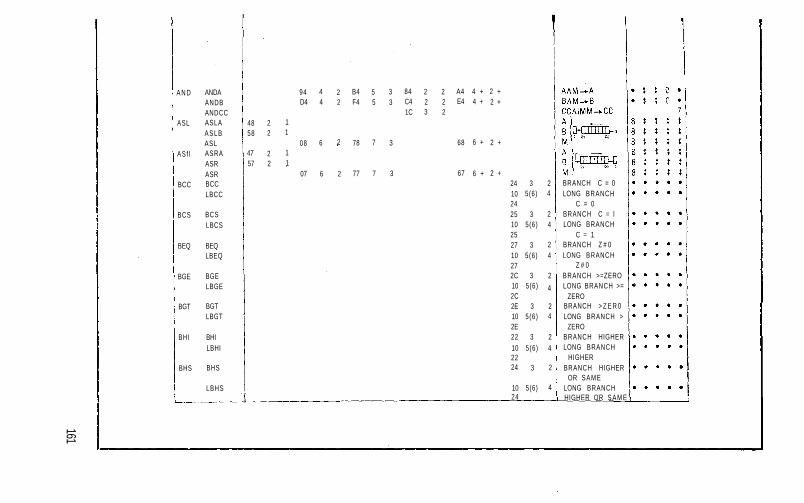
161
A N D
ASL
ASf l
BCC
BCS
BEQ
BGE
BGT
BHI
BHS
ANDA ANDB ANDCC ASLA ASLB ASL ASRA ASR ASR BCC LBCC
BCS LBCS
BEQ LBEQ
BGE LBGE
BGT LBGT
BHI LBHI
BHS
LBHS
48 58
47 57
2 2
2 2
1 1
1 1
94 D4
08
07
4 4
6
6
2 2
2
2
B4 F4
78
77
5 5
7
7
3 3
3
3
84 C4 1C
2 2 3
2 2 2
A4 E4
68
67
4 + 4 +
6 +
6 +
2 + 2 +
2 +
2 + 24 10 24 25 10 25 27 10 27 2C 10 2C 2E 10 2E 22 10 22 24
10 24
3 5(6)
3 5(6)
3 5(6)
3 5(6)
3 5(6)
3 5(6)
3
5(6)
2 4
2 4
2 4
2
4
2 4
2 4
2
4
BRANCH C = 0 LONG BRANCH
C = 0 BRANCH C = l LONG BRANCH
C = 1 BRANCH Z # 0 LONG BRANCH
Z # 0 BRANCH >=ZERO LONG BRANCH >=
ZERO BRANCH > Z E R 0 LONG BRANCH >
ZERO BRANCH HIGHER LONG BRANCH
HIGHER BRANCH HIGHER
OR SAME LONG BRANCH HIGHER OR S A M E

INSTRUCTION FORMS
BIT
BLE
BLO
BLS
BLT
BMI
BNE
BPL
BRA
BITA BITB BLE LBLE
BLO LBLO
BLS
LBLS
BLT LBLT
BMI LBMI
BNE LBNE
BPL LBPL
BRA LBRA
INHERENT OP ~ #
DIRECT OP 95 05
~ 4 4
# 2 2
6809 ADDRESSING MODES EXTENDED
OP B5 F5
~ 5 5
# 3 3
IMMEDIATE OP 85 C5
~ 2 2
# 2 2
INDEXED1
OP A5 E5
~ 4 + 4 +
# 2 + 2 +
RELATIVE OP
2F 10 2F 25 10 25 23
10 23
2D 10 2D 2B 10 2B 26 10 26 2A 10 2A 20 16
~5
3 5(6)
3 5(6)
3
5(6)
3 5(6)
3 5(6)
3 5(6)
3 5(6)
3 5
#
2 4
2 4
2
4
2 4
2 4
2 4
2 4
2 3
DESCRIPTION BIT TEST A(M A) BIT TEST B(M B) BRANCH ZERO LONG BRANCH ZERO
BRANCH LOWER LONG BRANCH
LOWER BRANCH LOWER
OR SAME LONG BRANCH
LOWER OR SAME
BRANCH <ZERO LONG BRANCH <
ZERO BRANCH MINUS LONG BRANCH
MINUS BRANCH Z = 0 LONG BRANCH
Z = 0 BRANCH PLUS LONG BRANCH
PLUS BRANCH ALWAYS LONG BRANCH Al WAYS
162
5 3 2 1 0 H N Z V C
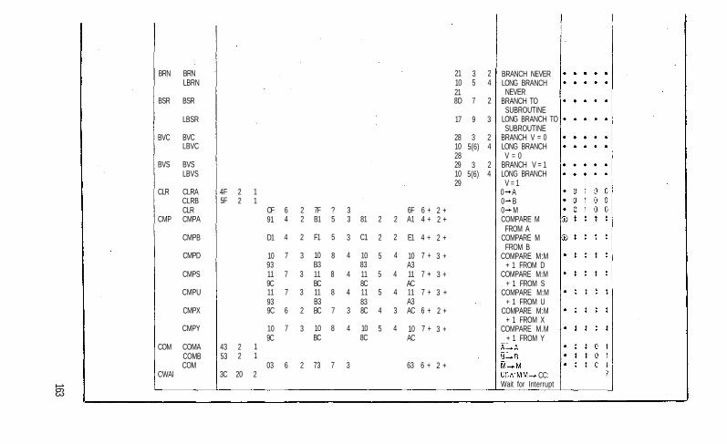
163
BRANCH NEVER LONG BRANCH NEVER
BRANCH TO SUBROUTINE
LONG BRANCH TO SUBROUTINE
BRANCH V = 0 LONG BRANCH
V = 0 BRANCH V = 1 LONG BRANCH
V = 1 0 A 0 B 0 M COMPARE M
FROM A COMPARE M
FROM B COMPARE M:M
+ 1 FROM D COMPARE M:M
+ 1 FROM S COMPARE M:M
+ 1 FROM U COMPARE M:M
+ 1 FROM X COMPARE M.M
+ 1 FROM Y
CC: Wait for Interrupt
BRN
BSR
BVC
BVS
CLR
CMP
COM
CWAI
BRN LBRN
BSR
LBSR
BVC LBVC
BVS LBVS
CLRA CLRB CLR CMPA
CMPB
CMPD
CMPS
CMPU
CMPX
CMPY
COMA COMB COM
4F 5F
43 53
3C
2 2
2 2
20
1 1
1 1
2
OF 91
D1
10 93 11 9C 11 93 9C
10 9C
03
6 4
4
7
7
7
6
7
6
2 2
2
3
3
3
2
3
2
7F B1
F1
10 B3 11 BC 11 B3 BC
10 BC
73
? 5
5
8
8
8
7
8
7
3 3
3
4
4
4
3
4
3
81
C1
10 83 11 8C 11 83 8C
10 8C
2
2
5
5
5
4
5
2
2
4
4
4
3
4
6F A1
E1
10 A3 11 AC 11 A3 AC
10 AC
63
6 + 4 +
4 +
7 +
7 +
7 +
6 +
7 +
6 +
2 + 2 +
2 +
3 +
3 +
3 +
2 +
3 +
2 +
21 10 21 8D
17
28 10 28 29 10 29
3 5
7
9
3 5(6)
3 5(6)
2 4
2
3
2 4
2 4

164
INSTRUCTION/ FORMS
DAA DEC
EOR
EXG INC
JMP JSR
LD
LEA
LSL
DECA DECB DEC EORA EORB R1, R2 INCA INCB INC
LDA LDB LDD LDS
LDU LDX LDY
LEAS LEAU LEAX LEAY LSLA LSLB LSL
INHERENT OP 19 4A 5A
1E 4C 5C
48 58
~ 2 2 2
8 2 2
2 2
# 1 1 1
2 1 1
1 1
DIRECT OP
OA 93 D8
0C 0E 9D
96 C6 DC 10 CE OE 9E 10 9E
08
~
S 4 4
6 3 7
4 4 5 6
5 5 6
6
#
2 2 2
2 2 2
2 2 2 3
2 2 3
2
6809 ADDRESSING MODES EXTENDED
OP
7A B8 F8
7C 7E BD
B6 F6 FC 10 FE FE BE 10 BE
78
~
7 5 5
7 4 8
5 5 6 7
6 6 7
7
#
3 3 3
3 3 3
3 3 3 4
3 3 4
3
IMMEDIATE OP
88 C8
86 C6 CC 10 CE CE 8E 10 8E
~
2 2
2 2 3 4
3 3 4
#
2 2
2 2 3 4
3 3 4
INDEXED1
OP
6A A8 E8
6C 6E AD
A6 E6 EC 10 EE EE AE 10 AE 32 33 30 31
68
~
6 + 4 + 4 +
6 + 3 + 7 +
4 + 4 + 5 + 6 +
5 + 5 + 6 +
4 + 4 + 4 + 4 +
6 +
#
2 + 2 + 2 +
2 + 2 + 2 +
2 + 2 + 2 + 3 +
2 + 2 + 3 +
2 + 2 + 2 + 2 +
2 +
RELATIVE OP ~5 # DESCRIPTION
5 3 2 1 0 H N Z V C
Decimal Adjust A
JUMP TO
SUBROUTINE

165
LSR
MUL
NEG
NOP OR
PSH
PUL
ROL
ROH
RTI
RTS
SBC
SEX
LSRA LSRB LSR
NEGA NEGB NEG
ORA ORB ORCC PSHS
PSHU
PULS
PULU
ROLA ROLB ROL RORA RORB ROR
SBCA SBCB
44 54
3D
40 50
12
34
36
35
37
49 59
46 56
3B
39
10
2 2
11
2 2
2
5 + 4
5 + 4
5 + 4
5 + 4
2 2
2 2
6/15
5
2
1
2
2
2
2
1
04
00
9A DA
09
06
92 D2
6
6
4 4
6
6
4 4
2
2
2 2
2
2
2 2
74
70
BA LA
79
76
B2 F2
7
7
5 5
7
7
5 5
3
3
3 3
3
3
3 3
8A CA 1A
82 C2
2 2 3
2 2
2 2 2
2 2
64
60
AA FA
69
66
A2 E2
6 +
6 +
4 + 4 +
6 +
6 +
4 + 4 +
2 +
2 +
2 + 2 +
2 +
2 +
2 + 2 +
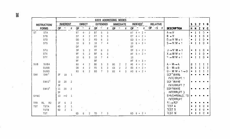
INSTRUCTION/ FORMS
ST STA STB STD STS
STU STX STY
S U B S U B A S U B B S U B D
SWI S W I 6
S W I 2 6
S W I 3 6
SYNC
TFR R1, R2 TST TSTA
TSTB TST
INHERENT OP
3F
10 3F 11 3F 13
1F 4D 5D
~
19
20
20
>=2
6 2 2
#
1
2
2
1
2 1 1
DIRECT OP 97 D7 DD 10 DF DF 9F 10 9F 90 D0 93
0D
~
4 4 5 6
5 5 6
4 4 6
6
# 2 2 2 3
2 2 3
2 2 2
2
6809 ADDRESSING MODES EXTENDED
OP B7 F7 FD 10 FF FF BF 10 BF B0 F0 B3
7D
~
5 5 6 7
6 6 7
5 5 7
7
# 3 3 3 4
3 3 4
3 3 3
3
IMMEDIATE OP
80 C0 83
~
2 2 4
#
2 2 3
INDEXED1
OP A7 E7 ED 10 EF EF AF 10 AF A0 E0 A3
6D
~
4 + 4 + 5 + 6 +
5 + 5 +
6 + 4 + 4 + 6 +
6 +
# 2 + 2 + 2 + 3 +
2 + 2 +
3 + 2 + 2 + 2 +
2 +
RELATIVE OP ~ 5 #
166

INDEXED ADDRESSING MODES
TYPE CONSTANT OFFSET FROM R
ACCUMULATOR OFFSET FROM R
AUTO INCREMENT/DECREMENT R
CONSTANT OFFSET FROM PC
EXTENDED INDIRECT
FORMS NO OFFSET
5 BIT OFFSET 8 BIT OFFSET
16 BIT OFFSET A—REGISTER OFFSET B—REGISTER OFFSEI D—REGISTER OFFSET INCREMENT BY 1 INCREMENT BY 2 DECREMENT BY 1 DECREMENT BY 2 8 BIT OFFSET 16 BIT OFFSET 16 BIT ADDRESS
NON INDIRECT ASSEMBLER
FORM R
n,R n,R n,R A ,R B,R D,R ,R+
, R + + ,-R
. - - R n,PCR n,PCR
—
POST-BYTE OP CODE
1RR00100 0RRnnnnn 1RR01000 1RR01001 1RR00110 1RR00101 1RR01011 1RR00000 1RR00001 1RR00010 1RR00011 1XX01100 1XX01101
—
+ ~ 0 1 1 4 1 1 4 2 3 2 3 1 5 —
+ # 0 0 1 2 0 0 0 0 0 0 0 1 2 —
INDIRECT ASSEMBLER
FORM [,R|
POST-BYTE OPCODE
1RR10100 DEFAULTS TO 8-BIT
[ n , R ] [ n , R ] [A,R] [B,R] [D,R]
1RR11000 1RR11001 1RR10110 1RR10101 1RR11011
NOT ALLOWED [ , R + + ] 1RR10001
NOT ALLOWED [ , - - R ] [n,PCR] [n,PCR]
[n]
1RR10011 1XX11100 1XX11101 10011111
+ ~
+ # 0
1 2 0 0 0
0
0 1 2 2
R = X, Y, U, or S
X = DON'T CARE
NOTES:
1. GIVEN IN THE TABLE ARE THE BASE CYCLES AND BYTE COUNTS TO DETERMINE THE TOTAL CYCLES AND BYTE COUNTS ADD THE VALUES
FROM THE 6809 INDEXING MODES' TABLE
2. R1 AND R2 MAY BE ANY PAIR OF 8 BIT OR ANY PAIR OF 16 BIT REGISTERS THE 8 BIT REGISTERS ARE: A, B, CC, DP THE 16 BIT REGISTERS ARE: X, Y, U, S, D, PC
X = 00 Y = 01
U = 10 S = 11
167

INDEXED ADDRESSING MODES
3 EA IS THE EFFECTIVE ADDRESS
4 THE PSH AND PUL INSTRUCTIONS REQUIRE 5 CYCLES PLUS 1 CYCLE FOR EACH BYTE PUSHED OR PULLED
5 5(6) MEANS: 5 CYCLES IF BRANCH NOT TAKEN. 6 CYCLES IF TAKEN.
6 SWI SETS I & F BITS. SWI2 AND SWI3 DO NOT AFFECT I & F.
7 CONDITIONS COOES SET AS A DIRECT RESULT OF THE INSTRUCTION
8 VALUE OF HALF-CARRY FLAG IS UNDEFINED.
9 SPECIAL CASE - CARRY SET IF b7 IS SET.
LEGEND: OP ~ # + -*
OPERATION CODE (HEXADECIMAL): NUMBER OF MPU CYCLES: NUMBER OF PROGRAM BYTES. ARITHMETIC PLUS: ARITHMETIC MINUS: MULTIPLY COMPLEMENT OF M:
H N Z V C
TRANSFER INTO; HALF-CARRY FROM BIT 3: NEGATIVE (SIGN BIT) ZERO (BYTE) OVERFLOW 2'S COMPLEMENT CARRY FROM BIT 7
• CC
V
TEST AND SET IF TRUE. CLEARED OTHERWISE
NOT AFFECTED CONDITION CODE REGISTER CONCATENATION LOGICAL OR LOGICAL AND LOGICAL EXCLUSIVE OR
168

Appendix D
Instruction Index MNEMONIC
ABX ADCA
ADCB
ADDA
ADDB
ADDD
ANDA
ANDB
A N D C C ASLA ASLB ASL
ASR
ADDRESSING MODE
INHERENT IMMEDIATE DIRECT INDEXED EXTENDED IMMEDIATE DIRECT INDEXED EXTENDED IMMEDIATE DIRECT INDEXED EXTENDED IMMEDAITE DIRECT INDEXED EXTENDED IMMEDIATE DIRECT INDEXED EXTENDED IMMEDIATE DIRECT INDEXED EXTENDED IMMEDIATE DIRECT INDEXED EXTENDED IMMEDIATE ACCUMULATOR ACCUMULATOR DIRECT EXTENDED INDEXED INHERENT
OP CODE
3A 89 99 A9 B9 C9 D9 E9 F9 8B 9B AB BB CB DB EB FB C3 D3 E3 F3 84 94 A4 B4 C4 D4 E4 C4 1C 48 58 08 78 68 57
169
CYCLES
3 2 4 4 + 5 2 4 4 + 5 2 4 4 + 5 2 4 4 + 5 4 6 6 + 7 2 4 4 + 5 2 4 4 + 5 3 2 2 6 7 6 + 2
PAGE NUMBER
59 60
60
61
61
61
63
63
63 64 64 64
65
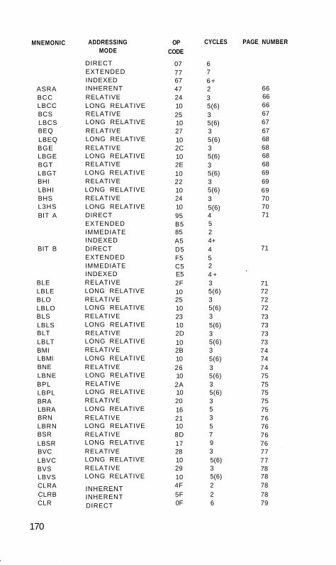
MNEMONIC
ASRA BCC LBCC BCS LBCS BEQ LBEQ BGE LBGE BGT LBGT BHI LBHI BHS L3HS BIT A
BIT B
BLE LBLE BLO LBLO BLS LBLS BLT LBLT BMI LBMl BNE LBNE BPL LBPL BRA LBRA BRN LBRN BSR LBSR BVC LBVC BVS LBVS CLRA CLRB CLR
ADDRESSING MODE
DIRECT EXTENDED INDEXED INHERENT RELATIVE LONG RELATIVE RELATIVE LONG RELATIVE RELATIVE LONG RELATIVE RELATIVE LONG RELATIVE RELATIVE LONG RELATIVE RELATIVE LONG RELATIVE RELATIVE LONG RELATIVE DIRECT EXTENDED IMMEDIATE INDEXED DIRECT EXTENDED IMMEDIATE INDEXED RELATIVE LONG RELATIVE RELATIVE LONG RELATIVE RELATIVE LONG RELATIVE RELATIVE LONG RELATIVE RELATIVE LONG RELATIVE RELATIVE LONG RELATIVE RELATIVE LONG RELATIVE RELATIVE LONG RELATIVE RELATIVE LONG RELATIVE RELATIVE LONG RELATIVE RELATIVE LONG RELATIVE RELATIVE LONG RELATIVE
INHERENT INHERENT DIRECT
OP CODE
07 77 67 47 24 10 25 10 27 10 2C 10 2E 10 22 10 24 10 95 B5 85 A5 D5 F5 C5 E5 2F 10 25 10 23 10 2D 10 2B 10 26 10 2A 10 20 16 21 10 8D 17 28 10 29 10 4F 5F 0F
CYCLES
6 7 6 + 2 3 5(6) 3 5(6) 3 5(6) 3 5(6) 3 5(6) 3 5(6) 3 5(6) 4 5 2 4+ 4 5 2 4 + 3 5(6) 3 5(6) 3 5(6) 3 5(6) 3 5(6) 3 5(6) 3 5(6) 3 5 3 5 7 9 3 5(6) 3 5(6) 2 2 6
PAGE NUMBER
66 66 66 67 67 67 68 68 68 68 69 69 69 70 70 71
71
71 72 72 72 73 73 73 73 74 74 74 75 75 75 75 75 76 76 76 76 77 77 78 78 78 78 79
170

171
MNEMONIC
CMPA
CMPB
CMPD
CMPS
CMPU
CMPX
CMPY
COMA COMB COM
CWAI
ADDRESSING MODE
EXTENDED INDEXED DIRECT EXTENDED IMMEDIATE INDEXED DIRECT EXTENDED IMMEDIATE INDEXED DIRECT
EXTENDED
IMMEDIATE
INDEXED
DIRECT
EXTENDED
IMMEDIATE
INDEXED
DIRECT
EXTENDED
IMMEDIATE
INDEXED
DIRECT EXTENDED IMMEDIATE INDEXED
DIRECT
EXTENDED
IMMEDIATE
INDEXED
INHERENT INHERENT DIRECT EXTENDED INDEXED INHERENT
OP CODE
7F 6F 91 B1 81 A1 D1 F1 C1 E1 10 93 10 B3 10 83 10 A3 11 9C 11 BC 11 8C 11 AC 11 93 11 B3 11 83 11 A3
9C BC 8C
A C
10C 9C 10 BC 10 8C 10 AC 43 53 03 73 63 3C
CYCLES
7 6 + 4 5 2 4 + 4 5 2 4 + 7
8
5
7 +
7
8
5
7 +
7
8
5
7 +
6 7 4 6 +
7
8
5
7 +
2 2 6 7 6 + 20
PAGE NUMBER
79
79
80
80
81
81
81
82 82 82
82

MNEMONIC
DAA DECA DECB DEC
EORA
EORB
EXG R 1 , R2 INCA INCB
INC
J MP
JSR
LDA
LDB
LDD
LDS
LDU
LDX
ADDRESSING MODE
INHERENT INHERENT INHERENT DIRECT EXTENDED INDEXED DIRECT EXTENDED IMMEDIATE INDEXED DIRECT EXTENDED IMMEDIATE INDEXED INHERENT INHERENT INHERENT
DIRECT EXTENDED INDEXED DIRECT EXTENDED INDEXED DIRECT EXTENDED INDEXED DIRECT EXTENDED IMMEDIATE INDEXED DIRECT EXTENDED IMMEDIATE INDEXED DIRECT EXTENDED IMMEDIATE INDEXED DIRECT
EXTENDED
IMMEDIATE
INDEXED
DIRECT EXTENDED IMMEDIATE INDEXED DIRECT EXTENDED
OP CODE
19 4A 5A OA 7A 6A 9B B8 88 A8 D8 F8 C8 E8 1E 4C 5C
0C 7C 6C OE 7E 6E 9D BD AD 96 B6 86 A6 D6 F6 C6 E6 DC FC CC EC 10 DE 10 FE 10 CE 10 EE DE FE CE EE 9E BE
1 7 2
CYCLES
2 2 2 6 7 6+ 4 5 2 4+ 4 5 2 4 + 7 2 2
6 7 6 + 3 4 3 + 7 8 7+ 4 5 2 4 + 4 5 2 4 + 5 6 3 5 + 6
7
4
6 +
5 6 3 5 + 5 6
PAGE NUMBER
84 85 85 85
85
86
86 87 87
87
87
88
88
88
89
89
89
89

MNEMONIC
LDY
LEAS LEAU LEAX LEAY LSLA LSLB LSL
LSRA LSRB LSR
MUL NEGA NEGB NEG
NOP ORA
ORB
ORCC PSHS PSHU PULS PULU ROLA ROLB ROL
RORA RORB ROR
ADDRESSING MODE
IMMEDIATE INDEXED DIRECT
EXTENDED
IMMEDIATE
INDEXED
RELATIVE RELATIVE RELATIVE RELATIVE INHERENT INHERENT DIRECT EXTENDED INDEXED INHERENT INHERENT DIRECT EXTENDED INDEXED INHERENT INHERENT INHERENT DIRECT EXTENDED INDEXED INHERENT DIRECT EXTENDED IMMEDIATE INDEXED DIRECT EXTENDED IMMEDIATE INDEXED IMMEDIATE INHERENT INHERENT INHERENT INHERENT INHERENT INHERENT DIRECT EXTENDED INDEXED INHERENT INHERENT DIRECT
173
OP CODE
8E A E 10 9F 10 BE 10 8E 10
A E
32 33 3 0 31 48 58 08 78 68 44 54 04 74 6 4 3 D 40 50 00 70 60 12 9A BA 8A A A DA FA CA EA 1A 34 36 35
37 49 59 09 79 69 46 56 06
CYCLES
3 5 + 6
7
4
6 +
4 + 4 + 4 + 4 + 2 2 6 7 6 + 2 2 6 7 6 + 11 2 2 6 7 6 + 2 4 5 2 4 + 4 5 2 4 + 3 5 + 4 5 + 4 5 + 4
5 + 4 2 2 6 7 6 + 2 2 6
PAGE NUMBER
89
90 90 90 90 91 91 91
92 92 92
93 93 93 93
94 94
94
95 96 96 96 97 98 98 98
99 99 99
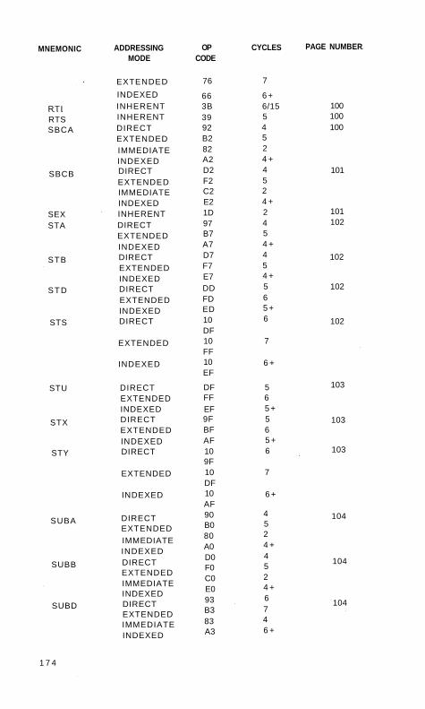
MNEMONIC
RTI RTS SBCA
SBCB
SEX STA
STB
S T D
STS
STU
STX
STY
SUBA
SUBB
SUBD
ADDRESSING MODE
EXTENDED
INDEXED INHERENT INHERENT DIRECT EXTENDED IMMEDIATE INDEXED DIRECT EXTENDED IMMEDIATE INDEXED INHERENT DIRECT EXTENDED INDEXED DIRECT EXTENDED INDEXED DIRECT EXTENDED INDEXED DIRECT
EXTENDED
INDEXED
DIRECT EXTENDED INDEXED DIRECT EXTENDED INDEXED DIRECT
EXTENDED
INDEXED
DIRECT EXTENDED IMMEDIATE INDEXED DIRECT EXTENDED IMMEDIATE INDEXED DIRECT EXTENDED IMMEDIATE INDEXED
1 7 4
OP CODE
76
66 3B 39 92 B2 82 A2 D2 F2 C2 E2 1D 97 B7 A7 D7 F7 E7 DD FD ED 10 DF 10 FF 10 EF
DF FF EF 9F BF AF 10 9F 10 DF 10 AF 90 B0 80 A0 D0 F0 C0 E0 93 B3 83 A3
CYCLES
7
6 + 6/15 5 4 5 2 4 + 4 5 2 4 + 2 4 5 4 + 4 5 4 + 5 6 5 + 6
7
6 +
5 6 5 + 5 6 5 + 6
7
6 +
4 5 2 4 + 4 5 2 4 + 6 7 4 6 +
PAGE NUMBER
100 100 100
101
101 102
102
102
102
103
103
103
104
104
104

MNEMONIC
SWI SWI2
SWI3
SYNC TFR TSTA TSTB TST
ADDRESSING MODE
INHERENT
INHERENT
INHERENT
INHERENT INHERENT INHERENT INHERENT DIRECT EXTENDED INDEXED
OP CODE
3F 10 3F 11 3F 13 1F 4D 5D OD 7D 6D
CYCLES
19 20
20
> = 2 7 2 2 6 7 6 +
PAGE NUMBER
105 105
106
107 108 109 109 109
175

Index
A Accumulator
offset indexed ADD Add to accumulator Addressing Addressing modes, basic
concepts innerent summary
Address it ALU American Microsystems Inc. AMI Arithmetic Logic Unit
operations Assembler, basics
listing typical requirements
Auto increment indexed
B Bit 5
4 1 7 6 3 2
BUSY Byte-oriented BitO
C Changed configuration Comment field Condition codes Constant offset indexed
D Direct addressing
Memory Access Page statements
DMA
E EA Effective address Enable input Error trapping
26 47 37 37
37-55
37 38 55 56 is 17 17 29
119 112 117 113 49
30 30 29 31 31 30 30 16 11 29
12 114
28,31 45
41 13 28
118 13
37 37 13
119
Edited by Robert E. Ostrander
176
Equivalencies Expressions Extended addressing
F Fast Interrupt Request FIRQ
H Halt/Bus grant Hardware Stack Pointer High level language processor
I Immediate addressing Indexed addressing
indirect Index registers Inherent addressing mode Interrupt Request
tracing IRQ
L Label field Last instruction Cycle LEA LIC Line numbering Load effective address
M Metal Oxide Substrate MOS Most Significant Bit MSB
0 Operand field Operating field
P Performance summary Pipelining effect Pointer
registers Preliminary concepts Processor busy signal Program Counter
statements
32 115 40
12 12
21 27 11
39 44 50 27 38 30 19 30
113 16 57 16
119 57
10 10 29 29
114 114
32 36 27 27
1.19 16 27
118
PSHU/PSHS Push/pull
Q Quadrature output
R Radio Shack TRS-80
Videotex Registers
addressing Relative addressing Right nomenclature
S Schmitt-trigger, pulling Set Direct Page Pointer SETDP Sequence number 6800/6809, software
incompatibilities 6809 mP, basics
condition codes individual instructions 59-interrupts introduction MPU signal description
Software interrupts
Statements SWI Symbols 9ync acknowledge System, establishing
variables 119,120
T Tri-state control TSC
U User Stack Pointer
V Variety in clocks VTL-09, sample programs
Z Zero-offset indexed
57 56
14
9 27 43 51 13
19 42 42
113
31 10 31
111 31 9
17 25 58
118 58
115 21 24
-124
15 15
27
13 124
45