december 2009 rev. 1.0 - future electronics · sp510 is ideal for space constrained applications....
TRANSCRIPT

SP510ULTRA HIGH SPEED MULTIPROTOCOL TRANSCEIVER
DECEMBER 2009 REV. 1.0.0
GENERAL DESCRIPTION The SP510 is a highly integrated physical layer solution that is configurable to support multiple serial standards. It incorporates eight (8) drivers and eight (8) receivers, configurable for either differential (V.11 or V.35) or single ended (V.28 and V.10) signaling. The device architecture is designed to support the data and clock signals used in HDLC or SDLC serial ports as either a DTE or DCE. SP510 enables a Serial Communications Controller (SCC) to implement a variety of serial port types including V.24, V.25, V.36, EIA-530, EIA-530-A, X.21, RS-232.
Operating configuration is in-system programmable using the mode-select pins. The V.11 and V.35 modes contain built in bus termination that may be switched in or out using the TERM_OFF pin.
SP510 is ideal for space constrained applications. It requires only a single 5V supply for full operation. The VL pin determines the receiver output voltage (VOH). For single supply operation at 5V the VL pin may be connected to VCC. Fully compliant V.28 and V.10 driver output voltages are generated using onboard charge pumps. Special power sequencing is not required during system startup. Charge pump outputs are internally regulated to minimize power consumption. The SP510 requires only four 1µF capacitors for complete functionality. The device may be put into a 1µA low power shutdown mode when not in active use.
All receivers have fail-safe protection to put outputs into a known state when inputs are open, terminated but open or shorted.
TYPICAL APPLICATIONS
• Data Communication Networks
• Telecommunication Equipment
• Secured Data Communication
• CSU and DSU
• Data Routers
• Network Switches
• WAN Access Equipment
• VoIP-PBX Gateways
Exar Corporation 48720 Kato Road, Fremont CA, 94538 • (5
FEATURES
• 52Mbps Differential Transmission Rates
• Adjustable Logic Level Pin (Down to 1.65V)
• +/-15kV ESD Tolerance for Analog I/O’s
• Internal Transceiver Termination Resistors for V.11/V.35
• Interface Modes:
RS-232 (V.28) EIA-530 (V.10 & V.11) X.21 (V.11) EIA-530A (V.10 & V.11) RS-449/V.36
• Software Selectable Protocols with 3-Bit Word
• Eight Drivers and Eight Receivers
• V.35/V.11 Receiver Termination Network Disable Option
• Internal Line or Digital Loopback Testing
• Adheres to NET1/NET2 and TBR2 Requirements
• Easy Flow-Through Pinout
• Single +5V Supply Voltage
• Individual Driver/Receiver Enable/Disable Controls
• Operates in DTE or DCE Mode
ORDERING INFORMATION
PART NUMBER PACKAGE OPERATING TEMPERATURE RANGE DEVICE STATUS
SP510EM 100-pin LQFP -40°C to +85°C Active
SP510CM 100-pin LQFP 0°C to +70°C Active
10) 668-7000 • FAX (510) 668-7017 • www.exar.com

SP510 ULTRA HIGH SPEED MULTIPROTOCOL TRANSCEIVER REV. 1.0.0
ABSOLUTE MAXIMUM RATINGS
These are stress ratings only and functional operation of the device at these ratings or any other above those indicated in the operation sections of the specifications below is not implied. Exposure to absolute maximum rating conditions for extended periods of time may affect reliability.
Supply Voltage (Vcc)……………...+ 7.0V
Logic-Interface Voltage (VL)………. VL ≤ Vcc
Input voltage at TTL input pins ... - 0.3V to VL+0.5V
Receiver Input voltage….. ………..±15.5V
Driver output (from Ground)…… -7.5V to +12.5V
Short Circuit Duration, TxOUT to GND, Continuous
2
Continuous Power Dissipation at Ta = +70° C
100-Pin QFP…………………….…1520 mW
(derate 19.0 mW / °C above 70° C)
ΘJA 52.7 °C/W, ΘJC 6.5 °C/W
Storage Temperature………...-65°C to +150°C
Lead Temperature (soldering, 10s)….. 300° C
RECOMMENDED OPERATING CONDITIONS
Supply Voltage (Vcc)... 4.75V to 5.25V
Logic-Interface Supply Voltage (VL)…..1.65V to 5.25V
Operating Temperature Range……-40° C to +85° C

SP510REV. 1.0.0 ULTRA HIGH SPEED MULTIPROTOCOL TRANSCEIVER
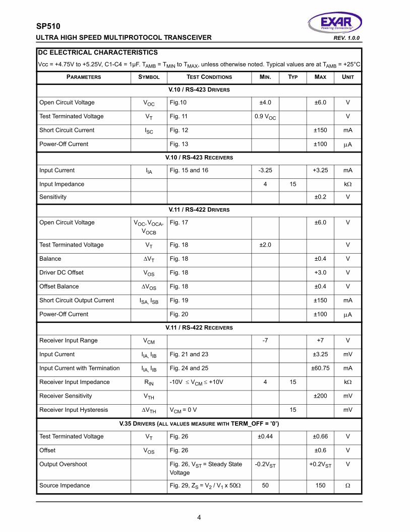
TABLE 1: DC ELECTRICAL CHARACTERISTICS
DC ELECTRICAL CHARACTERISTICS
Vcc = +4.75V to +5.25V, C1-C4 = 1µF. TAMB = TMIN to TMAX, unless otherwise noted. Typical values are at TAMB = +25°C
PARAMETERS SYMBOL TEST CONDITIONS MIN. TYP MAX UNIT
Vcc Supply Voltage VCC 4.75 5.25 V
Logic Interface Voltage VL VCC ≥ VL 1.65 5.25 V
ICC Shutdown ICCSD 200 µA
ICC Supply Current ICC 300 mA
DRIVER INPUT AND LOGIC INPUT PINS
Logic Input High VIH 2.0 V
Logic Input Low VIL 0.4 V
RECEIVER OUTPUTS
Receiver Logic Output Low VOL IOUT = -3.2 mA 0.4 V
Receiver Logic Output High VOH IOUT = 1 mA VL - 0.3 VL + 0.3 V
Receiver Output Short-Circuit Current
IOSS 0V < VO < VCC ±20 ±60 mA
Receiver Output Leakage Cur-rent
IOZ Receivers disabled. 0.4V < VO < 5.25V
±0.05 ±1 µA
V.28 / RS-232 DRIVERS
Output Voltage Swing VT Output load = 3kΩ to GND Fig. 3
±5.0 ±6.0 ±15.0 V
VOC Output load = Open CircuitFig.2
±15.0 V
Short Circuit Current ISC VOUT = 0V, Fig 5 ±100 mA
Power-Off Impedance Fig. 6 300 Ω
V.28 / RS-232 RECEIVERS
Input Voltage Range -15 15 V
Input Threshold Low 0.8 1.2 V
Input Threshold High 1.7 3.0 V
Input Hysteresis 500 mV
Input Resistance Fig. 8 3 5 7 kΩ
Open Circuit Bias VOC Fig. 9 ±2.0 V
3
SP510 ULTRA HIGH SPEED MULTIPROTOCOL TRANSCEIVER REV. 1.0.0
PARAMETERS SYMBOL TEST CONDITIONS MIN. TYP MAX UNIT
V.10 / RS-423 DRIVERS
Open Circuit Voltage VOC Fig.10 ±4.0 ±6.0 V
Test Terminated Voltage VT Fig. 11 0.9 VOC V
Short Circuit Current ISC Fig. 12 ±150 mA
Power-Off Current Fig. 13 ±100 µA
V.10 / RS-423 RECEIVERS
Input Current IIA Fig. 15 and 16 -3.25 +3.25 mA
Input Impedance 4 15 kΩ
Sensitivity ±0.2 V
V.11 / RS-422 DRIVERS
Open Circuit Voltage VOC, VOCA, VOCB
Fig. 17 ±6.0 V
Test Terminated Voltage VT Fig. 18 ±2.0 V
Balance ∆VT Fig. 18 ±0.4 V
Driver DC Offset VOS Fig. 18 +3.0 V
Offset Balance ∆VOS Fig. 18 ±0.4 V
Short Circuit Output Current ISA, ISB Fig. 19 ±150 mA
Power-Off Current Fig. 20 ±100 µA
V.11 / RS-422 RECEIVERS
Receiver Input Range VCM -7 +7 V
Input Current IIA, IIB Fig. 21 and 23 ±3.25 mV
Input Current with Termination IIA, IIB Fig. 24 and 25 ±60.75 mA
Receiver Input Impedance RIN -10V ≤ VCM ≤ +10V 4 15 kΩ
Receiver Sensitivity VTH ±200 mV
Receiver Input Hysteresis ∆VTH VCM = 0 V 15 mV
V.35 DRIVERS (ALL VALUES MEASURE WITH TERM_OFF = ’0’)
Test Terminated Voltage VT Fig. 26 ±0.44 ±0.66 V
Offset VOS Fig. 26 ±0.6 V
Output Overshoot Fig. 26, VST = Steady State Voltage
-0.2VST +0.2VST V
Source Impedance Fig. 29, ZS = V2 / V1 x 50Ω 50 150 Ω
DC ELECTRICAL CHARACTERISTICS
Vcc = +4.75V to +5.25V, C1-C4 = 1µF. TAMB = TMIN to TMAX, unless otherwise noted. Typical values are at TAMB = +25°C
4

SP510REV. 1.0.0 ULTRA HIGH SPEED MULTIPROTOCOL TRANSCEIVER
PARAMETERS SYMBOL TEST CONDITIONS MIN. TYP MAX UNIT
Short Circuit Impedance Fig. 28 135 165 Ω
V.35 RECEIVERS (ALL VALUES MEASURE WITH TERM_OFF = ’0’)
Sensitivity ±100 ±200 mV
Source Impedance Fig. 30, ZS = V2 / V1 x 50Ω 90 110 Ω
Short-Circuit Impedance Fig. 31 135 165 Ω
TRANSCEIVER LEAKAGE CURRENT
Driver Output 3-state Current Drivers disabled, per Fig. 32 500 µA
Receiver Output 3-state Current Tx and Rx Disabled, 0.4V - Vo - 2.4V
1 10 µA
DC ELECTRICAL CHARACTERISTICS
Vcc = +4.75V to +5.25V, C1-C4 = 1µF. TAMB = TMIN to TMAX, unless otherwise noted. Typical values are at TAMB = +25°C
5

SP510 ULTRA HIGH SPEED MULTIPROTOCOL TRANSCEIVER REV. 1.0.0
TABLE 2: AC TIMING CHARACTERISTICS
TIMING CHARACTERISTICS
VCC = +4.75 to 5.25V, C1-C4 = 1µF; TAMB = TMIN to TMAX, unless noted. Typical values are at TAMB = +25°C.
PARAMETERS SYMBOL TEST CONDITIONS MIN. TYP MAX UNIT
V.28 / RS-232
Maximum Transmission Rate Fig. 7 250 kbps
Driver Propagation Delay tDPHL, tDPLH
0.5 1 5 µs
Transition Time +3V to -3V, -3V to +3V per Fig. 7
0.2 1.5 µs
Instantaneous Slew Rate +3V to -3V, -3V to +3V per Fig. 4
4 30 V/µs
Driver Skew | tDPHL - tDPLH| at zero crossing
100 800 ns
Driver Channel to Channel Skew 20 ns
Driver Output Enable TimeTri-state to output Low
tZL CL = 100 pF, Fig. 34 and 40, S1 closed
2.0 µs
Driver Output Enable TimeTri-state to output High
tZH CL = 100 pF, Fig. 34 and 40, S2 closed
2.0 µs
Driver Output Disable TimeOutput Low to Tri-state
tLZ CL = 15 pF, Fig. 34 and 40, S1 closed
2.0 µs
Driver Output Disable TimeOutput High to Tri-state
tHZ CL = 15 pF, Fig. 34 and 40, S2 closed
20 µs
Receiver Propagation Delay tPHL, tPLH R_IN to R_OUT, CL = 15 pF 50 100 500 ns
Receiver Skew | tPHL - tPLH| at 1.5V 50 ns
Receiver Output Rise / Fall Time tR, tF CL = 15 pF 15 ns
Receiver Output Enable TimeTri-state to output Low
tZL CL = 100 pF, Fig. 35 and 40, S1 closed
2.0 µs
Receiver Output Enable TimeTri-state to output High
tZH CL = 100 pF, Fig. 35 and 40, S2 closed
2.0 µs
Receiver Output Disable TimeOutput Low to Tri-state
tLZ CL = 15 pF, Fig. 35 and 40,S1 closed
2.0 µs
Receiver Output Disable TimeOutput High to Tri-state
tHZ CL = 15 pF, Fig. 35 and 40,S2 closed
2.0 µs
Charge Pump Rise Time Shutdown to normal opera-tion
2 ms
V.10 / RS-423
Maximum Transmission Rate 250 kbps
6

SP510REV. 1.0.0 ULTRA HIGH SPEED MULTIPROTOCOL TRANSCEIVER
PARAMETERS SYMBOL TEST CONDITIONS MIN. TYP MAX UNIT
Driver Propagation Delay tPHL, tPLH 30 150 500 ns
Driver Rise / Fall Time tR, tF 10% to 90% - Fig. 14 500 ns
Driver Skew | tDPHL - tDPLH| at zero cross-ing
100 ns
Driver Output Enable TimeTri-state to Output Low
tZL CL = 100 pF, Fig. 34 and 40, S1 closed
2 µs
Driver Output Enable TimeTri-state to Output High
tZHCL = 100 pF, Fig. 34 and 40, S2 closed
2 µs
Driver Output Disable TimeOutput Low to Tri-state
tLZ CL = 15 pF, Fig. 34 and 40, S1 closed
2 µs
Driver Output Disable TimeOutput High to Tri-state
tHZ CL = 15 pF, Fig. 34 and 40, S2 closed
2 µs
Receiver Propagation Delay tPHL, tPLH 100 500 ns
Receiver Output Enable TimeTri-state to output Low
tZL CL = 100 pF, Fig. 35 and 40, S1 closed
2 µs
Receiver Output Enable TimeTri-state to output High
tZH CL = 100 pF, Fig. 35 and 40, S2 closed
2 µs
Receiver Output Disable TimeOutput Low to Tri-state
tLZ CL = 15 pF, Fig. 35 and 40, S1 closed
2 µs
Receiver Output Disable TimeOutput High to Tri-state
tHZ CL = 15 pF, Fig. 35 and 40, S1 closed
Receiver Output Rise / Fall Time tR, tF CL = 15 pF 15 ns
Receiver Skew | tPHL - tPLH| at 1.5V 5 ns
HIGH SPEED V.11 / RS-422 (DRIVERS 1, 2 & 3, RECEIVERS 1, 2 & 3)
Maximum Bit Rate NRZI Encoding 52 Mbps
Driver Rise and Fall Time tR, tF Fig. 22 and 36, 10-90% 0.5 6 ns
Propagation Delay Time tDPHL, tDPLH
Fig. 33 and 36, CL = 50 pF 5 25 ns
Differential Skew | tDPHL - tDPLH| 3.8 ns
Driver Output Enable TimeTri-state to Output Low
tZL CL = 100 pF, Fig. 34 and 37, S1 closed
100 ns
Driver Output Enable TimeTri-state to Output High
tZH CL = 100 pF, Fig. 34 and 37, S2 closed
100 ns
Driver Output Disable TimeOutput Low to Tri-state
tLZ CL = 15 pF, Fig. 34 and 37, S1 closed
100 ns
TIMING CHARACTERISTICS
VCC = +4.75 to 5.25V, C1-C4 = 1µF; TAMB = TMIN to TMAX, unless noted. Typical values are at TAMB = +25°C.
7

SP510 ULTRA HIGH SPEED MULTIPROTOCOL TRANSCEIVER REV. 1.0.0
PARAMETERS SYMBOL TEST CONDITIONS MIN. TYP MAX UNIT
Driver Output Disable TimeOutput High to Tri-state
tHZ CL = 15 pF, Fig. 34 and 37, S2 closed
100 ns
Receiver Propagation Delay tPHL, tPLH Fig. 33, 36CL = 50 pF
20 50 ns
Receiver Skew | tPHL - tPLH| Fig. 33, 36CL = 50 pF
3.8 ns
Receiver Output Enable TimeTri-state to Output Low
tZL CL = 100 pF, Fig. 35 and 39, S1 closed
100 ns
Receiver Output Enable TimeTri-state to Output High
tZH CL = 100 pF, Fig. 35 and 39, S2 closed
100 ns
Receiver Output Disable TimeOutput Low to Tri-state
tLZ CL = 15 pF, Fig. 35 and 39, S1 closed
100 ns
Receiver Output Disable TimeOutput High to Tri-state
tHZ CL = 15 pF, Fig. 35 and 39, S2 closed
100 ns
Receiver Output Rise / Fall Time tR, tF 3.0 V < VL < 5.5V1.65 V < VL < 3.0VCL = 50 pF
0.5 6 ns
Channel to channel Skew 2 ns
V.11 / RS-422 HANDSHAKE SIGNALS (DRIVERS 4, 5 & 6, RECEIVERS 4, 5 & 6)
Maximum Transmission Rate Fig. 33 10 Mbps
Driver Rise and Fall Time tR, tF Fig. 22 and 36 2 10 ns
Propagation Delay Time tDPHL, tDPLH
Fig. 33 and 36, CL = 50 pF 20 50 ns
Driver Propagation Delay Skew | tDPHL - tDPLH | 10 ns
Driver Channel to Channel Skew 2 ns
Driver Output Enable TimeTri-state to Output Low
tZL CL = 100 pF, Fig. 34 and 37, S1 closed
100 ns
Driver Output Enable TimeTri-state to Output High
tZH CL = 100 pF, Fig. 34 and 37, S2 closed
100 ns
Driver Output Disable TimeOutput Low to Tri-state
tLZ CL = 15 pF, Fig. 34 and 37, S1 closed
100 ns
Driver Output Disable TimeOutput High to Tri-state
tHZ CL = 15 pF, Fig. 34 and 37, S2 closed
100 ns
Receiver Propagation Delay tPHL, tPLH Fig. 33, 36CL = 50 pF
20 50 ns
TIMING CHARACTERISTICS
VCC = +4.75 to 5.25V, C1-C4 = 1µF; TAMB = TMIN to TMAX, unless noted. Typical values are at TAMB = +25°C.
8

SP510REV. 1.0.0 ULTRA HIGH SPEED MULTIPROTOCOL TRANSCEIVER
PARAMETERS SYMBOL TEST CONDITIONS MIN. TYP MAX UNIT
Receiver Skew | tPHL - tPLH| Fig. 33, 36CL = 50 pF
10 ns
Receiver Output Enable TimeTri-state to Output Low
tZL CL = 100 pF, Fig. 35 and 39, S1 closed
100 ns
Receiver Output Enable TimeTri-state to Output High
tZH CL = 100 pF, Fig. 35 and 39, S2 closed
100 ns
Receiver Output Disable TimeOutput Low to Tri-state
tLZ CL = 15 pF, Fig. 35 and 39, S1 closed
100 ns
Receiver Output Disable TimeOutput Low to Tri-state
tHZ CL = 15 pF, Fig. 35 and 39, S2 closed
100 ns
Receiver Output Rise / Fall Time tR , tF 1 20 ns
Channel to Channel Skew 2 ns
V.35 (DRIVERS 1, 2 & 3, RECEIVERS 1, 2 & 3)
Maximum Transmission Rate Fig. 33, fMAX = 20 MHz 40 Mbps
Driver Rise and Fall Time tR , tF Fig. 29 10 ns
Propagation Delay Time tDPHL , tDPLH
Fig. 33 and 36, CL = 50 pF 20 50 ns
Driver Differential Skew | tDPHL - tDPLH| Fig. 33 and 36
5.0 ns
Driver Channel to Channel Skew 2 ns
Driver Output Enable TimeTri-state to Output Low
tZL CL = 100 pF, Fig. 34 and 37, S1 closed
200 ns
Driver Output Enable TimeTri-state to Output High
tZH CL = 100 pF, Fig. 34 and 37, S2 closed
200 ns
Driver Output Disable TimeOutput Low to Tri-state
tLZ CL = 15 pF, Fig. 34 and 37, S1 closed
200 ns
Driver Output Disable TimeOutput High to Tri-state
tHZ CL = 15 pF, Fig. 34 and 37, S2 closed
200 ns
Receiver Propagation Delay tPHL , tPLH Fig. 33, 38CL = 50 pF
18 30 ns
Receiver Skew | tPHL - tPLH| Fig. 33 and 38CL = 50 pF
5.0 ns
Receiver Output Enable TimeTri-state to Output Low
tZL CL = 100 pF, Fig. 35 and 39, S1 closed
200 ns
TIMING CHARACTERISTICS
VCC = +4.75 to 5.25V, C1-C4 = 1µF; TAMB = TMIN to TMAX, unless noted. Typical values are at TAMB = +25°C.
9

SP510 ULTRA HIGH SPEED MULTIPROTOCOL TRANSCEIVER REV. 1.0.0
PARAMETERS SYMBOL TEST CONDITIONS MIN. TYP MAX UNIT
Receiver Output Enable TimeTri-state to Output High
tZH CL = 100 pF, Fig. 35 and 39, S2 closed
200 ns
Receiver Output Disable TimeOutput Low to Tri-state
tLZ CL = 15 pF, Fig. 35 and 39, S1 closed
200 ns
Receiver Output Disable TimeOutput High to Tri-state
tHZ CL = 15 pF, Fig. 35 and 39, S2 closed
200 ns
TIMING CHARACTERISTICS
VCC = +4.75 to 5.25V, C1-C4 = 1µF; TAMB = TMIN to TMAX, unless noted. Typical values are at TAMB = +25°C.
10
SP510REV. 1.0.0 ULTRA HIGH SPEED MULTIPROTOCOL TRANSCEIVER
FIGURE 1. PIN OUT DIAGRAM
SP510
TR(a
)G
ND
VDD
C1P
VCC
C2P
C1N
GN
DC
2NVS
S1
RL(
a)V
CC
LL(a
)TM
(a)
IC RR
T(a)
RR
T(b)
GN
DV
10D
M(a
)D
M(b
)C
S(a
)C
S(b)
TXC
(a)
GN
DTX
C(b
)
VL
GN
DS
DE
NTT
EN
STE
NR
SEN
TRE
NR
RC
ENR
LEN
LLE
N#
RD
EN#
RTE
N#
TXC
EN
#C
SE
N#
DM
EN
#R
RTE
N#
ICE
N#
TMEN D
0D
1D
2TE
RM
_OFF
D_L
ATC
H#
NC
GN
D
RT(a)RT(b)RD(a)RD(b)V35RGNDVLGNDTMRIDCD_DTEDSRCTSTXCRXCRXDLLRLDCD_DCEDTRRTSSTTX_CETXDLOOPBACK#VCC
NCVCC
TR(b)RRC(b)
VCCRRC(a)
GNDRS(a)VCC
RS(b)GND
ST(a)VCC
V35TGND3ST(b)GND
TT(a)VCC
V35TGND2TT(b)GND
SD(a)VCC
V35TGND1SD(b)
767778798081828384858687888990919293949596979899100
1 2 3 4 5 6 7 8 9 10 11 12 13 14 15 16 17 18 19 20 21 22 23 24 25
75 74 73 72 71 70 69 68 67 66 65 64 63 62 61 60 59 58 57 56 55 54 53 52 51
50494847464544434241403938373635343332313029282726
11
SP510 ULTRA HIGH SPEED MULTIPROTOCOL TRANSCEIVER REV. 1.0.0
TABLE 3: PIN DESCRIPTIONS BY FUNCTION
Pin Name Pin Number I/O DESCRIPTION
DIFFERENTIAL DRIVERS
TxD 28 I TTL TxD Driver Input
SD(b) / SD(a) 100, 97 O TTL Differential Transmit data non-inverting (b) and inverting (a) outputs
V35TGND1 99 I SD Termination Reference
SDEN 3 I TTL TxD Driver Enable
TxCE 29 I TTL TxCE Driver Input
TT(b) / TT(a) 95, 92 O TTL Differential TxCE non-inverting (b) and inverting (a) out-puts
V35TGND2 94 I TT Termination Reference
TTEN 4 I TTL TxCE Driver Enable
ST 30 I TTL ST Driver Input
ST(b) / ST(a) 90, 87 O TTL Differential ST non-inverting (b) and inverting (a) outputs
V35TGND3 89 I ST Termination Reference
STEN 5 I TTL ST Driver Enable
RTS 31 I TTL RTS Driver Input
RS(b) / RS(a) 85, 83 O TTL Differential RTS non-inverting (b) and inverting (a) outputs
RSEN 6 I TTL RTS Driver Enable
DTR 32 I TTL DTR Driver Input
TR(b) / TR(a) 78, 75 O TTL Differential DTR non-inverting (b) and inverting (a) outputs
TREN 7 I TTL DTR Driver Enable
DCD_DCE 33 I TTL DCD_DCE Driver Input
RRC(b) / RRC(a) 79, 81 O TTL Differential DCD non-inverting (b) and inverting (a) outputs
RRCEN 8 I TTL DCD Driver Enable
SINGLE ENDED DRIVERS
RL 34 I TTL RL Driver Input
RL(a) 65 O TTL RL Driver Output
RLEN 9 I TTL RL Driver Enable
LL 35 I TTL LL Driver Input
LL(a) 63 O TTL LL Driver Output
LLEN# 10 I TTL LL Driver Enable, active low
12

SP510REV. 1.0.0 ULTRA HIGH SPEED MULTIPROTOCOL TRANSCEIVER
DIFFERENTIAL RECEIVERS
RxD 36 O TTL RxD Receiver Output
RD(b) / RD(a) 47, 48 I TTL Differential RXD non-inverting (b) and inverting (a) inputs
RDEN# 11 I TTL RxD Receiver Enable, active low
RxC 37 O TTL RxC Receiver Output
RT(b) / RT(a) 49, 50 I TTL Differential RXC non-inverting (b) and inverting (a) inputs
RTEN# 12 I TTL RxC Receiver Enable, active low
TxC 38 O TTL TxC Receiver Output
TxC(b) / TxC(a) 51, 53 I TTL Differential TxC non-inverting (b) and inverting (a) inputs
TxCEN# 13 I TTL TxC Receiver Enable, active low
CTS 39 O TTL CTS Receiver Output
CS(b) / CS(a) 54, 55 I TTL Differential CTS non-inverting (b) and inverting (a) inputs
CSEN# 14 I TTL CTS Receiver Enable, active low
DSR 40 O TTL DSR Receiver Output
DM(b) / DM(a) 56, 57 I TTL Differential DSR non-inverting (b) and inverting (a) inputs
DMEN# 15 I TTL DSR Receiver Enable, active low
DCD_DTE 41 O TTL DCD_DTE Receiver Output
RRT(b) / RRT(a) 59, 60 I TTL Differential DCD_DTE non-inverting (b) and inverting (a) inputs
RRTEN# 16 I TTL DCD_DTE Receiver Enable, active low
SINGLE ENDED RECEIVERS
IC 61 I TTL RI Receiver Input
RI 42 O TTL RI Receiver Output
ICEN# 17 I TTL RI Receiver Enable, active low
TM(a) 62 I TTL TM Receiver Input
TM 43 O TTL TM Receiver Output
TMEN 18 I TTL TM Receiver Enable
PROTOCOL MODE SELECTION SIGNALS
D2, D1, D0 21, 20, 19 I TTL Mode Select - Refer to Table 5 and Table 6
Pin Name Pin Number I/O DESCRIPTION
13
SP510 ULTRA HIGH SPEED MULTIPROTOCOL TRANSCEIVER REV. 1.0.0
NOTE: Pin type: I = Input, O = Output, I/O = Input/output.
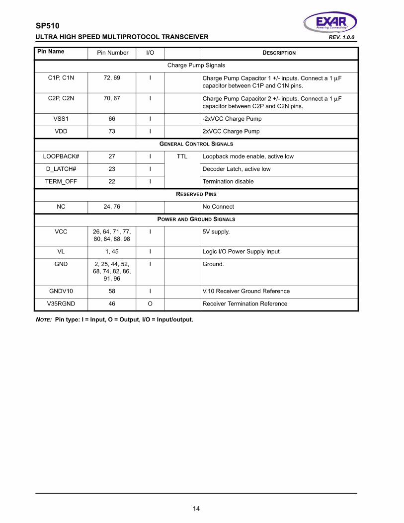
Charge Pump Signals
C1P, C1N 72, 69 I Charge Pump Capacitor 1 +/- inputs. Connect a 1 µF capacitor between C1P and C1N pins.
C2P, C2N 70, 67 I Charge Pump Capacitor 2 +/- inputs. Connect a 1 µF capacitor between C2P and C2N pins.
VSS1 66 I -2xVCC Charge Pump
VDD 73 I 2xVCC Charge Pump
GENERAL CONTROL SIGNALS
LOOPBACK# 27 I TTL Loopback mode enable, active low
D_LATCH# 23 I Decoder Latch, active low
TERM_OFF 22 I Termination disable
RESERVED PINS
NC 24, 76 No Connect
POWER AND GROUND SIGNALS
VCC 26, 64, 71, 77, 80, 84, 88, 98
I 5V supply.
VL 1, 45 I Logic I/O Power Supply Input
GND 2, 25, 44, 52, 68, 74, 82, 86,
91, 96
I Ground.
GNDV10 58 I V.10 Receiver Ground Reference
V35RGND 46 O Receiver Termination Reference
Pin Name Pin Number I/O DESCRIPTION
14

SP510REV. 1.0.0 ULTRA HIGH SPEED MULTIPROTOCOL TRANSCEIVER
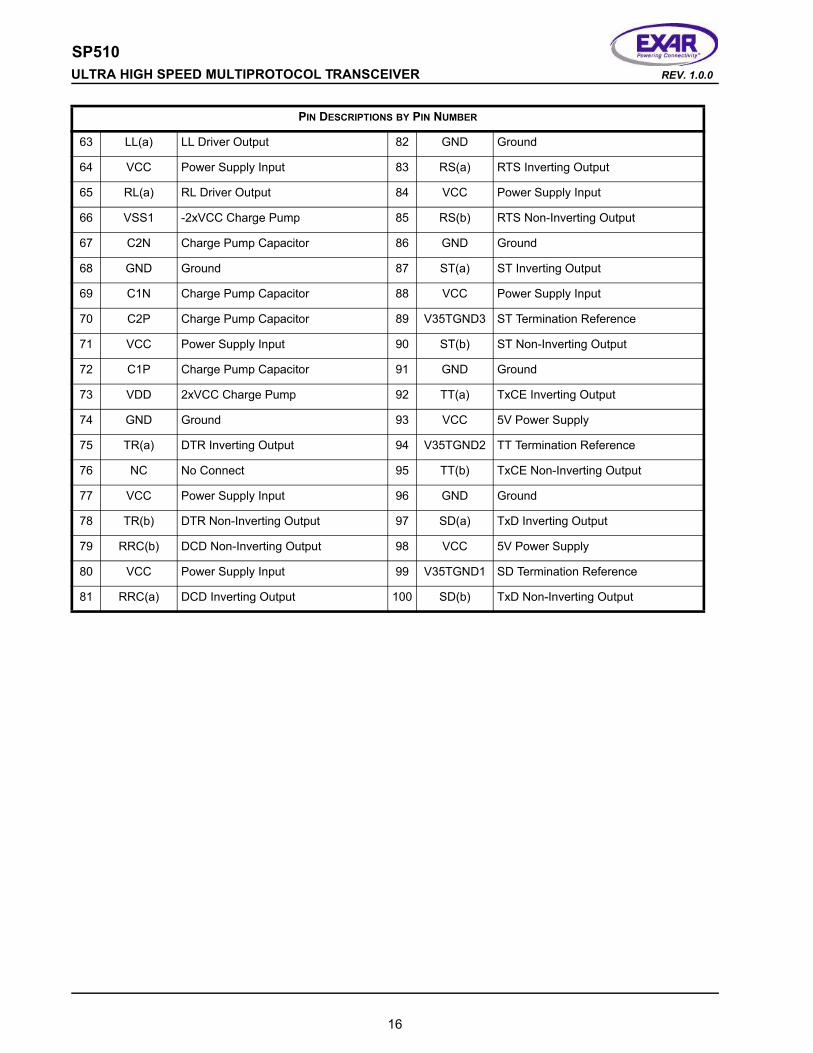
TABLE 4: PIN DESCRIPTIONS BY PIN NUMBER
PIN DESCRIPTIONS BY PIN NUMBER
1 VL Logic I/O Power Supply Input 32 DTR DTR Driver TTL Input
2 GND Ground 33 DCD_DCE DCD_DCE Driver TTL Input
3 SDEN TxD Driver Enable Input 34 RL RL Driver TTL Input
4 TTEN TxCE Driver Enable Input 35 LL LL Driver TTL Input
5 STEN ST Driver Enable Input 36 RxD RxD Receiver TTL Output
6 RSEN RTS Driver Enable Input 37 RxC RxC Receiver TTL Output
7 TREN DTR Driver Enable Input 38 TxC TxC Receiver TTL Output
8 RRCEN DCD Driver Enable Input 39 CTS CTS Receiver TTL Output
9 RLEN RL Driver Enable Input 40 DSR DSR Receiver TTL Output
10 LLEN# LL Driver Enable Input 41 DCD_DTE DCD_DTE Receiver TTL Output
11 RDEN# RxD Receiver Enable Input 42 RI RI Receiver TTL Output
12 RTEN# RxC Receiver Enable Input 43 TM TM Receiver TTL Output
13 TxCEN# TxC Receiver Enable Input 44 GND Ground
14 CSEN# CTS Receiver Enable Input 45 VL Logic I/O Power Supply Input
15 DMEN# DSR Receiver Enable Input 46 V35RGND Receiver Termination Reference
16 RRTEN# DCD_DTE Receiver Enable Input 47 RD(b) RXD Non-Inverting Input
17 ICEN# RI Receiver Enable Input 48 RD(a) RXD Inverting Input
18 TMEN TM Receiver Enable Input 49 RT(b) RxC Non-Inverting Input
19 D0 Mode Select Input - Bit 0 50 RT(a) RxC Inverting Input
20 D1 Mode Select Input - Bit 1 51 TxC(b) TxC Non-Inverting Input
21 D2 Mode Select Input - Bit 2 52 GND Ground
22 TERM_OFF Termination Disable Input 53 TxC(a) TxC Inverting Input
23 D_LATCH# Decoder Latch Input 54 CS(b) CTS Non-Inverting Input
24 NC No Connect 55 CS(a) CTS Inverting Input
25 GND Ground 56 DM(b) DSR Non-Inverting Input
26 Vcc Power Supply Input 57 DM(a) DSR Inverting Input
27 LOOP-BACK#
Loopback Mode Enable Input 58 GNDV10 V.10 Rx Ground Reference
28 TxD TxD Driver TTL Input 59 RRT(b) DCD_DTE Non-Inverting Input
29 TxCE TxCE Driver TTL Input 60 RRT(a) DCD_DTE Inverting Input
30 ST ST Driver TTL Input 61 IC RI Receiver Input
31 RTS RTS Driver TTL Input 62 TM(a) TM Receiver Input
15
SP510 ULTRA HIGH SPEED MULTIPROTOCOL TRANSCEIVER REV. 1.0.0
16
63 LL(a) LL Driver Output 82 GND Ground
64 VCC Power Supply Input 83 RS(a) RTS Inverting Output
65 RL(a) RL Driver Output 84 VCC Power Supply Input
66 VSS1 -2xVCC Charge Pump 85 RS(b) RTS Non-Inverting Output
67 C2N Charge Pump Capacitor 86 GND Ground
68 GND Ground 87 ST(a) ST Inverting Output
69 C1N Charge Pump Capacitor 88 VCC Power Supply Input
70 C2P Charge Pump Capacitor 89 V35TGND3 ST Termination Reference
71 VCC Power Supply Input 90 ST(b) ST Non-Inverting Output
72 C1P Charge Pump Capacitor 91 GND Ground
73 VDD 2xVCC Charge Pump 92 TT(a) TxCE Inverting Output
74 GND Ground 93 VCC 5V Power Supply
75 TR(a) DTR Inverting Output 94 V35TGND2 TT Termination Reference
76 NC No Connect 95 TT(b) TxCE Non-Inverting Output
77 VCC Power Supply Input 96 GND Ground
78 TR(b) DTR Non-Inverting Output 97 SD(a) TxD Inverting Output
79 RRC(b) DCD Non-Inverting Output 98 VCC 5V Power Supply
80 VCC Power Supply Input 99 V35TGND1 SD Termination Reference
81 RRC(a) DCD Inverting Output 100 SD(b) TxD Non-Inverting Output
PIN DESCRIPTIONS BY PIN NUMBER

SP510REV. 1.0.0 ULTRA HIGH SPEED MULTIPROTOCOL TRANSCEIVER
TABLE 5: DRIVER MODE SELECTION
DRIVER OUTPUT PIN MODE MODE
MODE (V.28) MODE
MODE (V.36) MODE
(V.11)
SHUT-DOWN
SUGGESTED SIGNAL
MODE (D2, D1, D0)
T1OUT(a) V.35 V.11 V.28 V.11 V.11 V.11 High-Z TxD(a)
T1OUT(b) V.35 V.11 High-Z V.11 V.11 V.11 High-Z TxD(b)
T2OUT(a) V.35 V.11 V.28 V.11 V.11 V.11 High-Z TxCE(a)
T2OUT(b) V.35 V.11 High-Z V.11 V.11 V.11 High-Z TxCE(b)
T3OUT(a) V.35 V.11 V.28 V.11 V.11 V.11 High-Z TxC_DCE(a)
T3OUT(b) V.35 V.11 High-Z V.11 V.11 V.11 High-Z TxC_DCE(b)
T4OUT(a) V.28 V.11 V.28 V.11 V.11 V.11 High-Z RTS(a)
T4OUT(b) High-Z V.11 High-Z V.11 V.11 V.11 High-Z RTS(b)
T5OUT(a) V.28 V.11 V.28 V.10 V.11 V.11 High-Z DTR(a)
T5OUT(b) High-Z V.11 High-Z High-Z V.11 V.11 High-Z DTR(b)
T6OUT(a) V.28 V.11 V.28 V.11 V.11 V.11 High-Z DCD_DCE(a)
T6OUT(b) High-Z V.11 High-Z V.11 V.11 V.11 High-Z DCD_DCE(b)
T7OUT(a) V.28 V.10 V.28 V.10 V.10 High-Z High-Z RL
T8OUT(a) V.28 V.10 V.28 V.10 V.10 High-Z High-Z LL
17
V.35 EIA-530 RS-232 EIA-530A
RS-449 X.21
001 010 011 100 101 110 111

SP510 ULTRA HIGH SPEED MULTIPROTOCOL TRANSCEIVER REV. 1.0.0
TABLE 6: RECEIVER MODE SELECTION
RECEIVER INPUT PIN MODE MODE
MODE (V.28) MODE
MODE (V.36) MODE
(V.11)
SHUT-DOWN
SUGGESTED SIGNAL
MODE (D2, D1, D0)
R1IN(a) V.35 V.11 V.28 V.11 V.11 V.11 High-Z RxD(a)
R1IN(b) V.35 V.11 High-Z V.11 V.11 V.11 High-Z RxD(b)
R2IN(a) V.35 V.11 V.28 V.11 V.11 V.11 High-Z RxCE(a)
R2IN(b) V.35 V.11 High-Z V.11 V.11 V.11 High-Z RxCE(b)
R3IN(a) V.35 V.11 V.28 V.11 V.11 V.11 High-Z TxC_DTE(a)
R3IN(b) V.35 V.11 High-Z V.11 V.11 V.11 High-Z TxC_DTE(b)
R4IN(a) V.28 V.11 V.28 V.11 V.11 V.11 High-Z CTS(a)
R4IN(b) High-Z V.11 High-Z V.11 V.11 V.11 High-Z CTS(b)
R5IN(a) V.28 V.11 V.28 V.10 V.11 V.11 High-Z DSR(a)
R5IN(b) High-Z V.11 High-Z High-Z V.11 V.11 High-Z DSR(b)
R6IN(a) V.28 V.11 V.28 V.11 V.11 V.11 High-Z DCD_DTE(a)
R6IN(b) High-Z V.11 High-Z V.11 V.11 V.11 High-Z DCD_DTE(b)
R7IN(a) V.28 V.10 V.28 V.10 V.10 High-Z High-Z RI
R8IN(a) V.28 V.10 V.28 V.10 V.10 High-Z High-Z TM
V.35 EIA-530 RS-232 EIA-530A
RS-449 X.21
001 010 011 100 101 110 111
18

SP510REV. 1.0.0 ULTRA HIGH SPEED MULTIPROTOCOL TRANSCEIVER
TABLE 7: V.11 & V.35 DRIVERS
INPUTS OUTPUTS
TX_EN# TX_IN TX(A) TX(B)
1 1 0 1
1 0 1 0
TABLE 8: V.11 & V.35 RECEIVERS
INPUTS OUTPUTS
RX(A) - RX(B)
≥ 200 mV 1
≤ −200 mV 0
Open / shorted 1
TABLE 9: V.28 DRIVERS
INPUTS OUTPUTS
TX_EN# TX_IN TX(A) TX(B)
1 1 < -5V > 30 kΩ
1 0 > +5V > 30 kΩ
TABLE 10: V.28 RECEIVERS
INPUTS OUTPUTS
RX(A) - RX(B)
≥ +3V 0
≤ −3V 1
Open / ground 1
RO
RO
1
TABLE 11: V.10 DRIVERS
INPUTS OUTPUTS
TX_EN# TX_IN TX(A) TX(B)
1 1 < -4V > 30 kΩ
1 0 > +4V > 30 kΩ
TABLE 12: V.10 RECEIVERS
INPUTS OUTPUTS
RX(A) - RX(B)
≥ +0.3V 0
≤ −0.3V 1
Open / ground 1
RO
9

SP510 ULTRA HIGH SPEED MULTIPROTOCOL TRANSCEIVER REV. 1.0.0
FIGURE 2. V.28 DRIVER OUTPUT OPEN CIRCUIT VOLT-AGE
FIGURE 3. V.28 DRIVER OUTPUT LOADED VOLTAGE
FIGURE 4. V.28 DRIVER OUTPUT SLEW RATE
2
FIGURE 5. V.28 DRIVER OUTPUT SHORT CIRCUIT CUR-RENT
FIGURE 6. V.28 DRIVER OUTPUT POWER-OFF IMPED-ANCE
FIGURE 7. V.28 DRIVER OUTPUT RISE/FALL TIME
0

SP510REV. 1.0.0 ULTRA HIGH SPEED MULTIPROTOCOL TRANSCEIVER
FIGURE 8. V.28 RECEIVER INPUT IMPEDANCE
FIGURE 9. V.28 RECEIVER INPUT OPEN-CIRCUIT BIAS
FIGURE 10. V.10 DRIVER OUTPUT OPEN-CIRCUIT VOLTAGE
2
FIGURE 11. V.10 DRIVER OUTPUT TEST TERMINATED VOLTAGE
FIGURE 12. V.10 DRIVER OUTPUT SHORT-CIRCUIT CURRENT
FIGURE 13. V.10 DRIVER OUTPUT POWER-OFF IMPED-ANCE
1

SP510 ULTRA HIGH SPEED MULTIPROTOCOL TRANSCEIVER REV. 1.0.0
FIGURE 14. V.10 DRIVER OUTPUT TRANSITION TIME
FIGURE 15. V.10 RECEIVER INPUT CURRENT
FIGURE 16. V.10 RECEIVER INPUT IV GRAPH
2
FIGURE 17. V.11 DRIVER OUTPUT TEST TERMINATED VOLTGE
FIGURE 18. V.11 DRIVER OUTPUT TEST TERMINATED VOLTAGE
FIGURE 19. V.11 DRIVER OUTPUT SHORT-CIRCUIT CURRENT
2

SP510REV. 1.0.0 ULTRA HIGH SPEED MULTIPROTOCOL TRANSCEIVER
FIGURE 20. V.11 DRIVER OUTPUT POWER-OFF CUR-RENT
A
B
C
Ixa
±0.25V
A
B
C
Ixb
±0.25V
VCC
= 0V
VCC
= 0V
2
FIGURE 21. V.11 RECEIVER INPUT CURRENT
A
B
C
Iia
±10V
C
Iib
±10V
A
B
3

SP510 ULTRA HIGH SPEED MULTIPROTOCOL TRANSCEIVER REV. 1.0.0
FIGURE 22. V.11 DRIVER OUTPUT RISE/FALL TIME
FIGURE 23. V.11 RECEIVER INPUT IV GRAPH
2
FIGURE 24. V.11 RECEIVER INPUT CURRENT WITH TER-MINATION
A
B
C
Iia
±6V
C
Iib
±6V
A
B
100 to150
100 to150
4

SP510REV. 1.0.0 ULTRA HIGH SPEED MULTIPROTOCOL TRANSCEIVER
FIGURE 25. V.11 RECEIVER INPUT IV GRAPH WITH TERMINATION
FIGURE 26. V.35 DRIVER OUTPUT TEST TERMINATED VOLTAGE
FIGURE 27. V.35 DRIVER OUTPUT SOURCE IMPEDANCE
25

SP510 ULTRA HIGH SPEED MULTIPROTOCOL TRANSCEIVER REV. 1.0.0
FIGURE 28. V.35 DRIVER OUTPUT SHORT-CIRCUIT IMPEDANCE
FIGURE 29. V.35 DRIVER OUTPUT RISE/FALL TIME
FIGURE 30. V.35 RECEIVER INPUT SOURCE IMPEDANCE
26

SP510REV. 1.0.0 ULTRA HIGH SPEED MULTIPROTOCOL TRANSCEIVER
FIGURE 31. V.35 RECEIVER INPUT SHORT-CIRCUIT IMPEDANCE
FIGURE 32. DRIVER OUTPUT CURRENT LEAKAGE TEST
FIGURE 33. DRIVER / RECEIVER TIMING TEST CIRCUIT
27

SP510 ULTRA HIGH SPEED MULTIPROTOCOL TRANSCEIVER REV. 1.0.0
FIGURE 34. DRIVER TIMING TEST LOAD CIRCUIT
FIGURE 35. RECEIVER TIMING TEST LOAD CIRCUIT
FIGURE 36. DRIVER PROPAGATON DELAYS
28

SP510REV. 1.0.0 ULTRA HIGH SPEED MULTIPROTOCOL TRANSCEIVER
FIGURE 37. DRIVER ENABLE AND DISABLE TIMES
FIGURE 38. RECEIVER PROPAGATION DELAYS
FIGURE 39. RECEIVER ENABLE AND DISABLE TIMES
29

SP510 ULTRA HIGH SPEED MULTIPROTOCOL TRANSCEIVER REV. 1.0.0
FIGURE 40. V.28 (RS-232) AND V.10 (RS-423) DRIVER ENABLE AND DISABLE TIMES
FIGURE 41. TYPICAL V.28 DRIVER OUTPUT WAVEFORM
30

SP510REV. 1.0.0 ULTRA HIGH SPEED MULTIPROTOCOL TRANSCEIVER
FIGURE 42. TYPICAL V.10 DRIVER OUTPUT WAVEFORM
FIGURE 43. TYPICAL V.11 DRIVER OUTPUT WAVEFORM
FIGURE 44. TYPICAL V.35 DRIVER OUTPUT WAVEFORM
31

SP510 ULTRA HIGH SPEED MULTIPROTOCOL TRANSCEIVER REV. 1.0.0
FIGURE 45. FUNCTIONAL DIAGRAM
TxD
SD(a)
V35TGND1
SD(b)
SDEN
VCC
VDD
C1-
VSS
C1+
+5V (decoupling capacitor not shown)
1µF
Regulated Charge Pump
SP510
TxCE
TT(a)
V35TGND2
TT(b)
TTEN
ST
ST(a)
V35TGND3
ST(b)
STEN
RD(a)
RxD
RDEN
RD(b)
RT(a)
RxC
RTEN
RT(b)
TxC(a)
TxC
TxCEN
TxC(b)
CS(a)
CTS
CSEN
CS(b)
DM(a)
DSR
DMEN
DM(b)
RRT(a)
DCD_DTE
RRTEN
RRT(b)
TM(a)
TM
TMEN
RTS
RS(a)
RS(b)
RSEN
DTR
TR(a)
TR(b)
TREN
DCD_DCE
RRC(a)
RRC(b)
RRCEN
LL
LL(a)
LLEN
C2-C2+
GND
D0
D1
D2
TERM-OFF
D-LATCH
V.10-GND
V.35 MODE
TX ENABLE
51ohms
51ohms
124ohms
V.35 DRIVER TERMINATION NETWORK
V.35 MODE
RX ENABLE
51ohms
51ohms
124ohms
RECEIVER TERMINATION NETWORK
V.11 MODE
RL
RL(a)
RLEN
IC
RI
ICEN
V35RGND
LOOPBACK
72 69 70 67
6673
46
48
36
11
47
50
37
12
49
53
3813
51
55
39
14
54
57
4015
56
60
41
16
59
61
42
17
62
43
18
19
20
21
23
22
27
28
97
99
100
3
29
92
94
95
4
30
87
89
90
5
31
83
85
6
32
75
78
7
33
81
79
8
34
65
9
35
63
10
58
VCC pins (26, 64, 71, 77, 80, 84, 88, 93, 98)
GND pins (2, 25, 44, 52, 68, 74, 82, 86, 91, 96)
N.C. pins (24 and 76)1µF
1µF
1µF
Logic Voltage
VL
VL pins (1 and 46)
32
SP510REV. 1.0.0 ULTRA HIGH SPEED MULTIPROTOCOL TRANSCEIVER
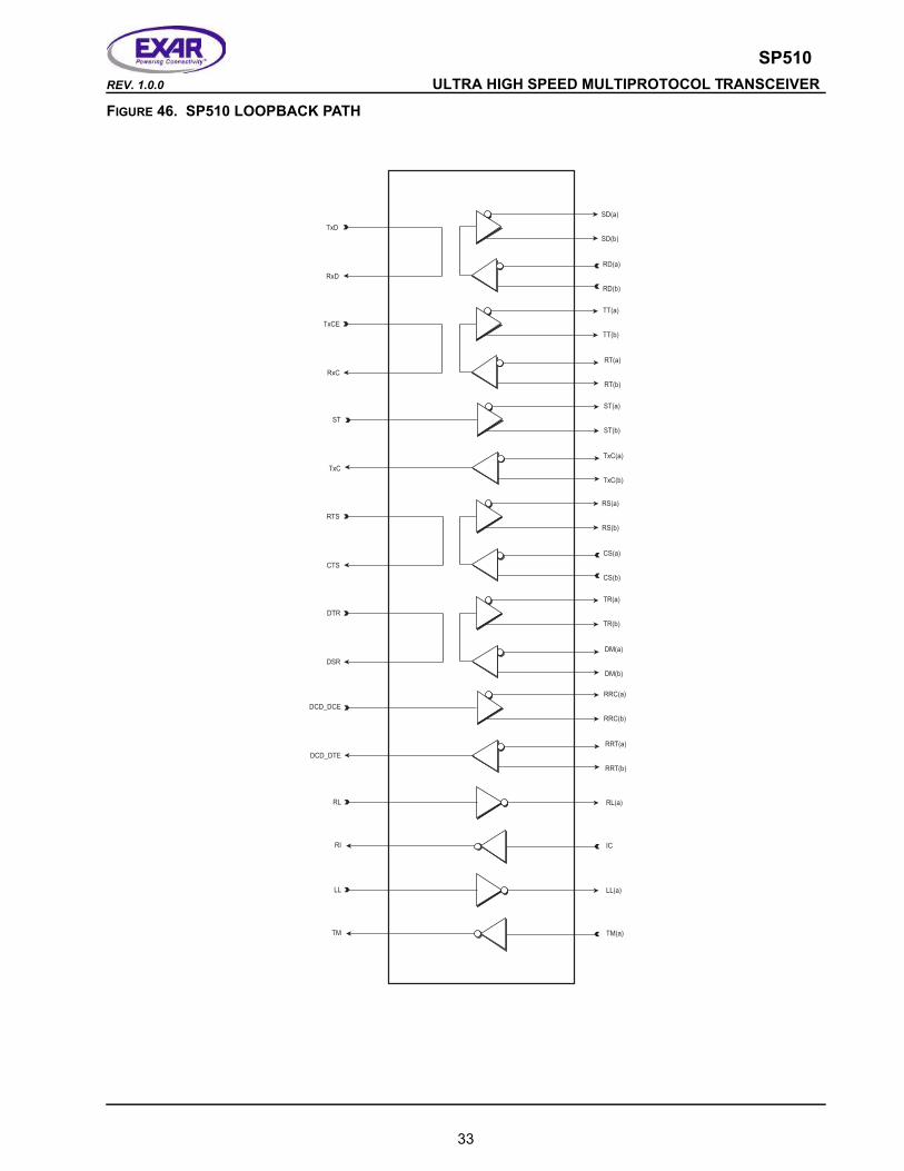
FIGURE 46. SP510 LOOPBACK PATH
SD(a)
SD(b)
RD(a)
RD(b)
TT(a)
TT(b)
RT(a)
RT(b)
TxD
RxD
TxCE
RxC
ST(a)
ST(b)
TxC(a)
TxC(b)
ST
TxC
RS(a)
RS(b)
CS(a)
CS(b)
TR(a)
TR(b)
DM(a)
DM(b)
RTS
CTS
DTR
DSR
RRC(a)
RRC(b)
RRT(a)
RRT(b)
DCD_DCE
DCD_DTE
RL(a)
IC
RL
RI
LL(a)
TM(a)
LL
TM
33

SP510 ULTRA HIGH SPEED MULTIPROTOCOL TRANSCEIVER REV. 1.0.0
FIGURE 47. TYPICAL OPERATING CONFIGURATION TO SERIAL PORT CONNECTOR WITH DCE/DTE PROGRAMMABIL-ITY
20 (V
.11,
V.28
)D
TR_D
SR_A
23 (V
.11)
DTR
_DSR
_B
1µF
1µF
1µF
VC
C
VD
DC
1-C
2- VS
S
C1+
C2+
1µF
SP
510
TxD
TxC
E ST
RTS
DTR
DC
D_D
CE RL
RxC TxC
CTS DS
R
DC
D_D
TE RI
TM
10µ
F
µD
B-26
Ser
ial P
ort C
onne
ctor
Pin
s
Si
gnal
(DTE
_DC
E)
2 (V
.11,
V.35
,V.2
8)TX
D_R
XD_A
14 (V
.11,
V.35
)TX
D_R
XD_B
11 (V
.11,
V.35
)TX
CE_
TXC
_B
25 (V
.10,
V.28
)LL
_TM
15 (V
.11,
V.35
,V.2
8)*T
XC_R
XC_A
12 (V
.11,
V.35
)*T
XC_R
XC_B
SD
EN
24 (V
.11,
V.35
,V.2
8)TX
CE_
TXC
_A
3 (V
.11,
V.35
,V.2
8)R
XD_T
XD_A
16 (V
.11,
V.35
)R
XD_T
XD_B
8 (V
.11,
V.28
)D
CD
_DC
D_A
10 (V
.11)
DC
D_D
CD
_B
Typi
cal S
P51
0 D
B-2
6 S
eria
lPor
t Con
figur
atio
n
Cust
om
er:
Titl
e:
Date
:D
oc.
# :
Rev
.
0
Ref
eren
ce D
esig
n S
chem
atic
SIG
NAL
GN
D (1
0 Pi
ns)
9 (V
.11,
V.35
)R
XC_T
XCE_
B17
(V.1
1,V.
35,V
.28)
RXC
_TXC
E_A
LLE
N
STE
N
GN
D
* -
Dri
ver
applie
s fo
r D
CE
only
on p
ins
15 a
nd 1
2.
Rece
iver
applie
s fo
r D
TE
only
on p
ins
15 a
nd 1
2.
+5
V
#103 (
TxD
)
#108 (
DT
R)
#105 (
RT
S)
#141 (
LL)
#105 (
RX
D)
#115 (
RX
C)
#106 (
CT
S)
#107 (
DS
R)
#109 (
DC
D) D
TE
I/O Li
nes r
epre
sente
d by d
ouble
arro
whea
d sign
ifies a
bi-d
irecti
onal
bus.
Input
Line
Outpu
t Line
#114 (
TxC
)
#113 (
TX
CE
)
#109 (
DC
D) D
CE
LL
RxD
TTE
N
TRE
N
RS
EN
RR
CE
N
RLE
N
RD
EN
TME
N
TxC
EN
RTE
N
DM
EN
CS
EN
RR
TEN
ICE
NV
10_G
ND
V35
TGN
D1
V35
TGN
D2
V35
TGN
D3
V35
RG
ND
TER
M_O
FF
D_L
ATC
HD0
D1
D2
Cha
rge
Pum
p S
ectio
n
Tran
scei
ver S
ectio
n
Logi
c S
ectio
nV
L
21 (V
.10,
V.28
)R
L_R
I
22 (V
.10,
V.28
)R
I_R
L
18 (V
.10,
V.28
)LL
_TM
#125 (
RI)
#142 (
TM
)
#140 (
RL)
DC
E/D
TE
Dri
ver
applie
s fo
r D
CE
only
on p
ins
8 a
nd 1
0.
Rece
iver
applie
sfo
r D
TE
only
on p
ins
8 a
nd 1
0.
LOO
PB
ACK
VL
19 (V
.11)
RTS_
CTS
_B4
(V.1
1,V.
28)
RTS_
CTS
_A
6 (V
.11,
V.28
)D
SR_D
TR_A
22 (V
.11)
DSR
_DTR
_B
13 (V
.11)
CTS
_RTS
_B5
(V.1
1,V.
28)
CTS
_RTS
_A
VL
Logic
Volta
ge
34

SP510REV. 1.0.0 ULTRA HIGH SPEED MULTIPROTOCOL TRANSCEIVER
Thermal Considerations
High speed devices like the SP510 dissipate heat during normal operation. Actual power dissipation is a function of the switching frequency and loading. For maximum system performance and reliability designers should ensure sufficient air flow. Other commonly used methods for managing heat include heat sinks for higher powered devices, forced air flow (fans) and lower density board stuffing.
PCB Design
The use of multi layer printed circuit boards is recommended to provide both a better ground plane and a thermal path for heat dissipation. If possible, the ground plane should face the bottom of the package to form the thermal conduction plane. Two-sided printed circuit boards may be used where board dimensions and package count are small, but multi-layer boards allow for improved signal routing as well as improved signal integrity. A multi layer board allows the use of microstrip line techniques to provide for high speed signal interconnections. On multi-layer boards route the high speed signal lines on the inner layers.
35

SP510 ULTRA HIGH SPEED MULTIPROTOCOL TRANSCEIVER REV. 1.0.0
36

SP510REV. 1.0.0 ULTRA HIGH SPEED MULTIPROTOCOL TRANSCEIVER
REVISION HISTORY
DATE REVISION DESCRIPTION
December 2009 Rev 1.0.0 Final datasheet.
37
NOTICE
EXAR Corporation reserves the right to make changes to the products contained in this publication in order to improve design, performance or reliability. EXAR Corporation assumes no responsibility for the use of any circuits described herein, conveys no license under any patent or other right, and makes no representation that the circuits are free of patent infringement. Charts and schedules contained here in are only for illustration purposes and may vary depending upon a user’s specific application. While the information in this publication has been carefully checked; no responsibility, however, is assumed for inaccuracies.
EXAR Corporation does not recommend the use of any of its products in life support applications where the failure or malfunction of the product can reasonably be expected to cause failure of the life support system or to significantly affect its safety or effectiveness. Products are not authorized for use in such applications unless EXAR Corporation receives, in writing, assurances to its satisfaction that: (a) the risk of injury or damage has been minimized; (b) the user assumes all such risks; (c) potential liability of EXAR Corporation is adequately protected under the circumstances.
Copyright 2009 EXAR Corporation
Datasheet December 2009.
Send your UART technical inquiry with technical details to hotline: [email protected].
Reproduction, in part or whole, without the prior written consent of EXAR Corporation is prohibited.