decay spectroscopy at fair with aida
DESCRIPTION
Decay Spectroscopy at FAIR with AIDA. presented by Tom Davinson on behalf of the AIDA collaboration (Edinburgh – Liverpool – STFC DL & RAL). Tom Davinson School of Physics & Astronomy The University of Edinburgh. Presentation Outline. r-process Nuclear Physics Observables FAIR - PowerPoint PPT PresentationTRANSCRIPT
Decay Spectroscopy at FAIR with AIDA
presented byTom Davinson
on behalf of the AIDA collaboration(Edinburgh – Liverpool – STFC DL & RAL)
Tom DavinsonSchool of Physics & AstronomyThe University of Edinburgh

Presentation Outline
• r-process• Nuclear Physics Observables• FAIR• SuperFRS• Decay Spectroscopy (DESPEC)• Advanced Implantation Detector Array (AIDA)
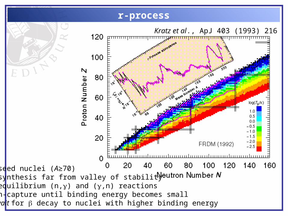
r-process
• seed nuclei (A≥70)• synthesis far from valley of stability • equilibrium (n,) and (,n) reactions• n-capture until binding energy becomes small• wait for decay to nuclei with higher binding energy
Kratz et al., ApJ 403 (1993) 216

r-process: Nuclear physics observables
Observable Effect
Sn path
T1/2 • abundance pattern
• timescale
Pn freezeout abundance pattern
Primary nuclear physics observables from studying the decay spectroscopy(principally and -delayed neutron emission) of r-process nuclei

•Cost
–Approx €1000M
–€650M central German government
–€100M German regional funding
–€250M from international partners
•Timescale
–Feb 2006- German funds in budget 2007-14
–2007 project start
–2016 phased start experiments
–2018 completion
NUSTAR
SuperFRS
Future facilityFuture facility100 m
GSI todayGSI today
SIS 100/300
UNILAC
ESR
SIS 18
HESR
RESR
NESR
FAIR: Facility for Antiproton and Ion Research

FAIR: SuperFRS layout
courtesy of Martin Winkler, GSI
Fast radioactive beams can be used to study r-process• chemistry independent• fast production• measure several nuclei simultaneously• measurements possible with low rates

FAIR: Production Rates
from FAIR CDR, section 2
Predicted Lifetimes > 100ns

DESPEC: Implantation DSSD Concept
• SuperFRS, Low Energy Branch (LEB)• Exotic nuclei – energies ~ 50 – 200MeV/u• Implanted into multi-plane, highly segmented DSSD array• Implant – decay correlations• Multi-GeV DSSD implantation events• Observe subsequent p, 2p, p, n … low energy (~MeV) decays• Measure half lives, branching ratios, decay energies …• Tag interesting events for gamma and neutron detector arrays

Implantation DSSD Configurations
Two configurations proposed:
a) 8cm x 24cm “cocktail” mode many isotopes measured simultaneously
b) 8cm x 8cm concentrate on particular isotope(s) high efficiency mode using:
total absorption spectrometermoderated neutron detector array

Implantation – Decay Correlation
• DSSD strips identify where (x,y) and when (t0) ions implanted
• Correlate with upstream detectors to identify implanted ion type
• Correlate with subsequent decay(s) at same position (x,y) at times t1(,t2, …)
• Observation of a series of correlations enables determination of energy distribution and half-life of radioactive decay
• Require average time between implants at position (x,y) >> decay half-lifedepends on DSSD segmentation and implantation rate/profile
• Implantation profilex ~ y ~ 2cm, z ~ 1mm
• Implantation rate (8cm x 24cm) ~ 10kHz, ~ kHz per isotope (say)
• Longest half life to be observed ~ seconds
Implies quasi-pixel dimensions ~ 0.5mm x 0.5mm
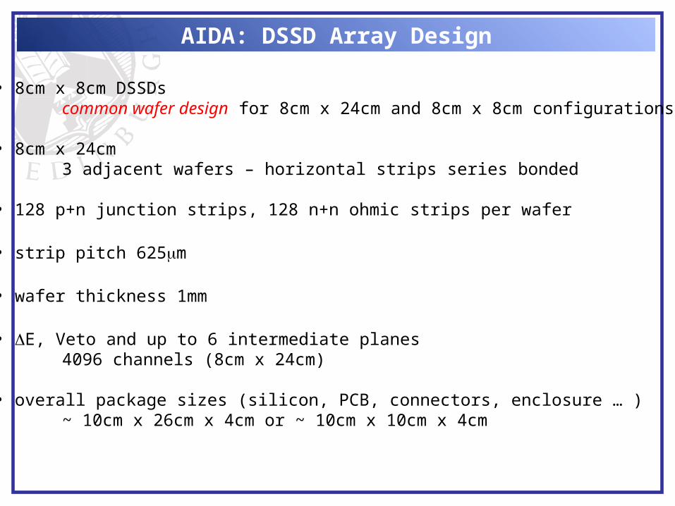
AIDA: DSSD Array Design
• 8cm x 8cm DSSDscommon wafer design for 8cm x 24cm and 8cm x 8cm configurations
• 8cm x 24cm3 adjacent wafers – horizontal strips series bonded
• 128 p+n junction strips, 128 n+n ohmic strips per wafer
• strip pitch 625m
• wafer thickness 1mm
• E, Veto and up to 6 intermediate planes4096 channels (8cm x 24cm)
• overall package sizes (silicon, PCB, connectors, enclosure … )~ 10cm x 26cm x 4cm or ~ 10cm x 10cm x 4cm

ASIC Design Requirements
Selectable gain 20 1000 20000 MeV FSRLow noise 12 600 50000 keV FWHM
energy measurement of implantation and decay events
Selectable threshold < 0.25 – 10% FSRobserve and measure low energy detection efficiency
Integral non-linearity < 0.1% and differential non-linearity < 2% for > 95% FSRspectrum analysis, calibration, threshold determination
Autonomous overload detection & recovery ~ sobserve and measure fast implantation – decay correlations
Nominal signal processing time < 10sobserve and measure fast decay – decay correlations
Receive (transmit) timestamp datacorrelate events with data from other detector systems
Timing trigger for coincidences with other detector systemsDAQ rate management, neutron ToF

Schematic of Prototype ASIC Functionality
Note – ASIC will also evaluate use of digital signal processing
Potential advantages• decay – decay correlations to ~ 200ns• pulse shape analysis• ballistic deficit correction
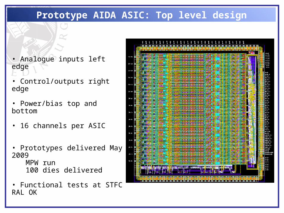
• Analogue inputs left edge
• Control/outputs right edge
• Power/bias top and bottom
• 16 channels per ASIC
• Prototypes delivered May 2009MPW run100 dies delivered
• Functional tests at STFC RAL OK
Prototype AIDA ASIC: Top level design

AIDA ASIC simulation: example
0 1 2 3 4 5 6 7 8 9 10 11 12 13 14 15I_LF fdbk=0
I_LF fdbk=6.4
I_LF fdbk=12.81.00E -041.10E -041.20E -041.30E -041.40E -041.50E -041.60E -041.70E -041.80E -041.90E -042.00E -04
Noise [V rm s]
S ha ping T ime (from 0.5us to 8us)
AIDA rms NOIS E : I_L F fdbk vs S haping T ime (C det=4.7pF , Ibias _preAmp=8)
1.90E -04-2.00E -04
1.80E -04-1.90E -04
1.70E -04-1.80E -04
1.60E -04-1.70E -04
1.50E -04-1.60E -04
1.40E -04-1.50E -04
1.30E -04-1.40E -04
1.20E -04-1.30E -04
1.10E -04-1.20E -04
1.00E -04-1.10E -04
Optimum ASIC parameters identified by simulation

Prototype AIDA ASIC

Fixed high-energy (HE) event (610pC) followed by three ME events (15pC, 30pC, 45pC): the ASIC recovers autonomously from the overload of the L-ME channel and the second event is read correctly.
Input signals (voltage step capacitive-coupled)
Preamp buffered output(Low-Medium Energy Channel)
“Range” signalHigh = high-energy channel active
“Data Ready” signal
3: High Energy (HE) + ME
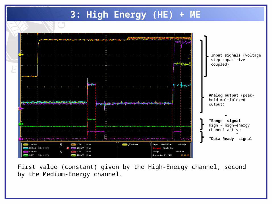
First value (constant) given by the High-Energy channel, second by the Medium-Energy channel.
Input signals (voltage step capacitive-coupled)
“Range” signalHigh = high-energy channel active
“Data Ready” signal
Analog output (peak-hold multiplexed output)
3: High Energy (HE) + ME

FEE Assembly Sequence

AIDA: status• Systems integrated prototypes available
- prototype tests in progress• Production planned Q3/2010
Mezzanine: 4x 16 channel ASICs Cu cover EMI/RFI/light screen cooling
FEE: 4x 16-bit ADC MUX readout (not visible) 8x octal 50MSPS 14-bit ADCs Xilinx Virtex 5 FPGA PowerPC 40x CPU core – Linux OS
Gbit ethernet, clock, JTAG portsPower
FEE width: 8cmPrototype – air coolingProduction – recirculating coolant
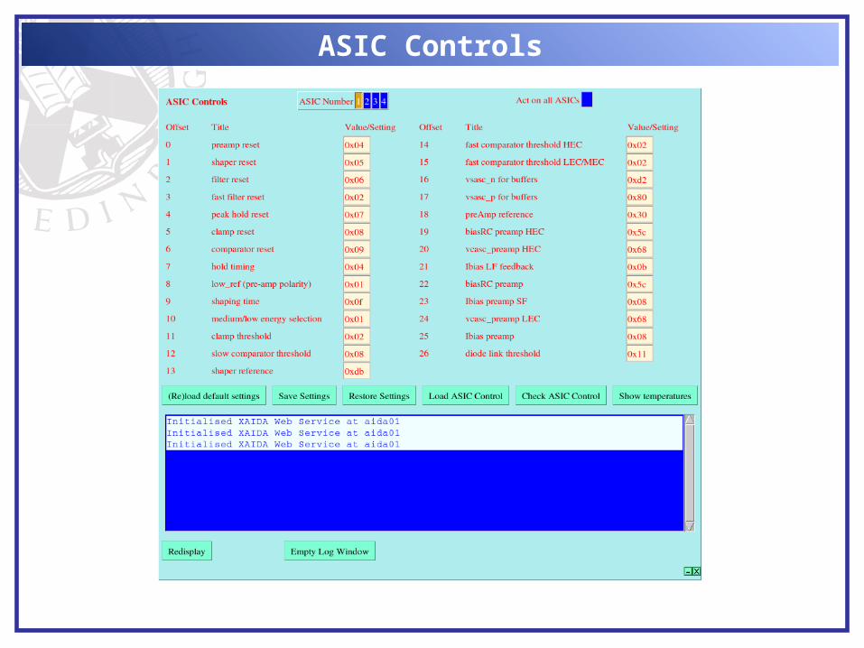
ASIC Controls

Examples of prototype bench tests
1keV = 61V0.15mV rms ~ 2.5keV rms Si
Test range ~ 20k channels

Prototype AIDA Enclosure
- Design drawings (PDF) available http://www.eng.dl.ac.uk/secure/np-work/AIDA/

AIDA Enclosure
• Prototype mechanical design• Based on 8cm x 8cm DSSSD
evaluate prior to design for 24cm x 8cm DSSSD• Compatible with RISING, TAS, 4 neutron detector
• 12x 8cm x 8cm DSSSDs 24x AIDA FEE cards
• 3072 channels
• Design complete
• Mechanical assembly in progress

AIDA
AIDA: outlook
• DSSSD with sub-contractor (MSL)
• ASIC submitted for wafer production run (AMS)– delivery January 2011
• FEE mezzanine PCB – will be submitted for manufacture Nov 2010– delivery January 2011
• FEE PCB with sub-contractor- delivery January 2011
• Mechanical design and infrastructure (HV, PSUs, cooling etc.)- STFC DL & University of Liverpool arranging manufacture/purchase
Production complete hardware now available for integration/initial tests
AIDA expected to be ready for commissioning/first experiments from 2011/Q3
Continuing development work in progress, e.g. MWD, integration with otherdetector systems

AIDA: Project Partners
• The University of Edinburgh (lead RO)Phil Woods et al.
• The University of LiverpoolRob Page et al.
• STFC DL & RALJohn Simpson et al.
Project Manager: Tom Davinson
Further information: http://www.ph.ed.ac.uk/~td/AIDA
Technical Specification:http://www.ph.ed.ac.uk/~td/AIDA/Design/AIDA_Draft_Technical_Specification_v1.pdf

Acknowledgements
My thanks to:
STFC DLPatrick Coleman-Smith, Ian Lazarus, Simon Letts, Paul Morrall, Vic Pucknell, John Simpson & Jon Strachan
STFC RALDavide Braga, Mark Prydderch & Steve Thomas
University of LiverpoolTuomas Grahn, Paul Nolan, Rob Page, Sami Ritta-Antila & Dave Seddon
University of EdinburghZhong Liu, Phil Woods
Prototype AIDA hardware tests at MARSLivius Trache et al., Cyclotron Institute, Texas A&M


Heavy Element Abundance: Solar System
from B.S.Meyer, Ann. Rev. Astron. Astrophys. 32 (1994) 153
Si=106
r-process produces roughly one-half of all elements heavier than iron

Heavy element nucleosynthesis
Process Environment Timescale Endpoint Site
s-process (n,)
T9~0.1
n>>n~1-1000a
n~108/cm3
<106a 209Bi AGB stars
r-process (n,)
T9~1-2
n<<n~s
n~1024-1030/cm3
<1s beyond U Type II supernovae?
NS-NS mergers?
p-process T9~2-3 ~1s Type II supernovae

r-process: What do observations tell us?
12log)(logH
NN
X xε
from Cowan & Sneden, Nature 440 (2006) 1151
CS22892-052• galactic halo star (intermediate population II)• red giant• ‘metal poor’ [Fe/H] = -3.0
solar
loglog]/[
Y
X
Y
X
NN
NN
YX
Matches relative elementalsolar abundance pattern
• common site/event type?• applies to ‘metal poor’ and ‘metal rich’ stars – rapid evolution of old stars?

r-process: U/Th Cosmo-chronology
from Cowan & Sneden, Nature 440 (2006) 1151
(13.8±4)Ga
(14.1±2.5)Ga
Cowan et al., ApJ 572 (2002) 861
Wanajo et al., ApJ 577 (2002) 853
• long half-lives• very similar mass• r-process production only

r-process: -delayed neutron emission
Effect of -delayed neutron emission:modification (smoothing) of final abundance pattern at freezeout
• Sn<Q
• increasing N → lower Sn,higher Q
Kratz et al., ApJ 403 (1993) 216
before -decay after -decay

Proposed layout August 2006(for illustrative purposes – way out of date!)
courtesy of Martin Winkler, GSI
FAIR: HISPEC/DESPEC

AIDA: ASIC schematic
High-speed bufferx10
DC fdbk
shaper
9R
R
Slowcomparator
Clamp comparator(for x10)
PeakHoldpositivePolarity
PeakHoldnegativePolarity
RC filter(with reset)
Fastcomparator
RC filter(with reset)
CM
OS
sw
itches
I thresholdR threshold
I thresholdR threshold
DC fdbk
shaperPeakHold
positivePolarity
PeakHoldnegativePolarity
Fastcomparator
RC filter(with reset)
I thresholdR threshold
4:1 MUX
1
2
2
3 4
4
5
6
6
7
8
9
9
10
10
10
10
1010
11
11
11
11
1111
12
13
14
14
15
16
17
18
18
1919
1919
19
19
19
19
19
19