dc2428a 4-channel pmbus power system manager with …€¦ · 1 2428 demo manual dc2428a...
TRANSCRIPT

1dc2428afa
DEMO MANUAL DC2428A
Description
LTC29754-Channel PMBus Power System Manager
with LTM4644 Quad 4A Power Supply
The DC2428A is a two-board demonstration system consisting of the DC2382A and DC2363A. The DC2382A contains all the circuitry needed to use the LTC®2975 Power System Manager to control four power supplies. The DC2363A contains four power supplies (LTM4644-1 quad 4A µModule® regulator) that the LTC2975 configures and controls. The DC2363A and DC2382A demo boards together provide a sophisticated 4-channel digitally pro-grammable power supply system.
The LTC2975 is a 4-channel I2C/SMBus/PMBus power system manager that features accurate input current and energy measurement. The device monitors input current and input voltage, and calculates input power and energy. The DC2382A demonstrates the ability of the LTC2975 to sequence, trim, margin, supervise, monitor, and log faults for four power supplies. Each power supply chan-nel’s output voltage and output current is monitored and the LTC2975 monitors its own internal die temperature.
The DC2363A is a single circuit board that contains four independent power supply rails. The board employs a single LTM4644 4-channel 4A DC/DC regulator. The board comes pre-configured with 1V, 1.5V, 2.5V, and 3.3V supply rails and may be reconfigured with feedback resistors.
The LTpowerPlay® graphical user interface (GUI) supports this demonstration system and enables complete control of all the features of the LTC2975. Together, the LTpowerPlay software and DC2428A hardware system create a powerful development environment for designing and testing con-figuration settings of the LTC2975. LTpowerPlay stores these settings in the LTC2975’s internal EEPROM or in a project file. The software displays all of the configuration settings and real time measurements from the Power System Management IC. Telemetry allows easy access and decoding of the fault log created by the LTC2975. The board comes pre-programmed with the EEPROM
L, LT, LTC, LTM, Linear Technology, µModule, LTpowerPlay and the Linear logo are registered trademarks of Linear Technology Corporation. All other trademarks are the property of their respective owners.
values appropriate for the four power supply rails on the DC2428A. Just plug and play!
The following items are required:
• +12VDC Power Supply
• USB-to-I2C/SMBus/PMBus Controller (DC1613)
• LTpowerPlay Software
DC2428A Features
• Sequence, Trim, Margin, and Supervise Four Power Supplies
• Manage Faults, Monitor Telemetry, and Create Fault Logs
• PMBus Compliant Command Set
• Supported by LTpowerPlay GUI
• Margin or Trim Supplies to 0.25% Accuracy
• Four IOUT and One IIN Monitor
• Input Power Measurement and Energy Accumulation
• Fast OV/UV Supervisors Per Channel
• Multi-Channel Fault Management
• Automatic Fault Logging to Internal EEPROM
• Operates Autonomously without Additional Software
• Monitors: Voltage, Current, Power, Temperature
• 4-Channel Time-Based Output Sequencer
• I2C/SMBus Serial Interface
• Powered from 4.5V to 14V
Design files for this circuit board are available at http://www.linear.com/demo/DC2428A
2dc2428afa
DEMO MANUAL DC2428A
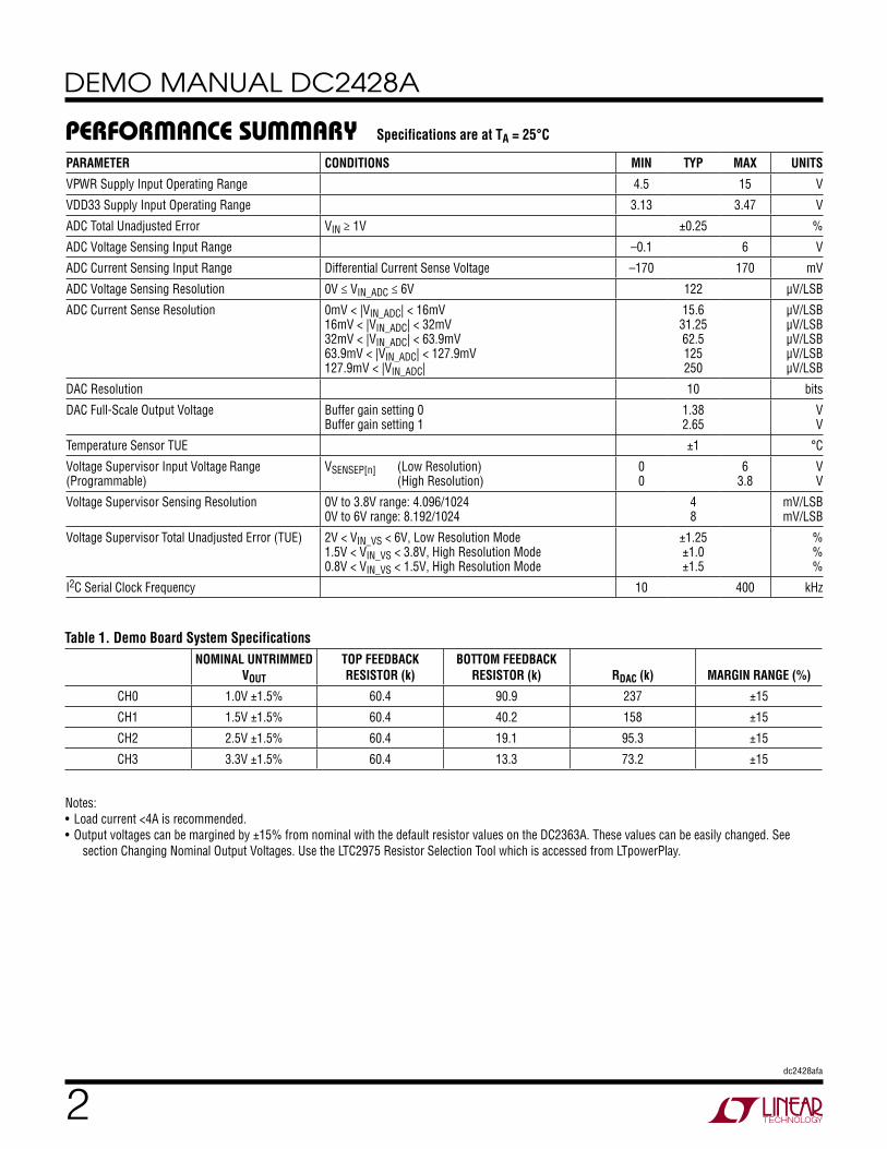
performance summary Specifications are at TA = 25°C
PARAMETER CONDITIONS MIN TYP MAX UNITS
VPWR Supply Input Operating Range 4.5 15 V
VDD33 Supply Input Operating Range 3.13 3.47 V
ADC Total Unadjusted Error VIN ≥ 1V ±0.25 %
ADC Voltage Sensing Input Range –0.1 6 V
ADC Current Sensing Input Range Differential Current Sense Voltage –170 170 mV
ADC Voltage Sensing Resolution 0V ≤ VIN_ADC ≤ 6V 122 µV/LSB
ADC Current Sense Resolution 0mV < |VIN_ADC| < 16mV 16mV < |VIN_ADC| < 32mV 32mV < |VIN_ADC| < 63.9mV 63.9mV < |VIN_ADC| < 127.9mV 127.9mV < |VIN_ADC|
15.6 31.25 62.5 125 250
µV/LSB µV/LSB µV/LSB µV/LSB µV/LSB
DAC Resolution 10 bits
DAC Full-Scale Output Voltage Buffer gain setting 0 Buffer gain setting 1
1.38 2.65
V V
Temperature Sensor TUE ±1 °C
Voltage Supervisor Input Voltage Range (Programmable)
VSENSEP[n] (Low Resolution) (High Resolution)
0 0
6 3.8
V V
Voltage Supervisor Sensing Resolution 0V to 3.8V range: 4.096/1024 0V to 6V range: 8.192/1024
4 8
mV/LSB mV/LSB
Voltage Supervisor Total Unadjusted Error (TUE) 2V < VIN_VS < 6V, Low Resolution Mode 1.5V < VIN_VS < 3.8V, High Resolution Mode 0.8V < VIN_VS < 1.5V, High Resolution Mode
±1.25 ±1.0 ±1.5
% % %
I2C Serial Clock Frequency 10 400 kHz
Table 1. Demo Board System SpecificationsNOMINAL UNTRIMMED
VOUT
TOP FEEDBACK RESISTOR (k)
BOTTOM FEEDBACK RESISTOR (k) RDAC (k) MARGIN RANGE (%)
CH0 1.0V ±1.5% 60.4 90.9 237 ±15
CH1 1.5V ±1.5% 60.4 40.2 158 ±15
CH2 2.5V ±1.5% 60.4 19.1 95.3 ±15
CH3 3.3V ±1.5% 60.4 13.3 73.2 ±15
Notes: • Loadcurrent<4Aisrecommended.•Outputvoltagescanbemarginedby±15%fromnominalwiththedefaultresistorvaluesontheDC2363A.Thesevaluescanbeeasilychanged.See
section Changing Nominal Output Voltages. Use the LTC2975 Resistor Selection Tool which is accessed from LTpowerPlay.

3dc2428afa
DEMO MANUAL DC2428A
Glossary of termsThe following list contain terms used throughout the document.
Channel: The collection of functions that monitor, super-vise, and trim a given power supply rail.
EEPROM: Non-volatile memory (NVM) storage used to retain data after power is removed.
Margin: Term used typically in board level testing that increases/decreases the output voltage to look for sensi-tivity/marginality problems.
Monitor: The act of measuring voltage, current, and tem-perature readings.
NVM: Non-volatile memory, see EEPROM.
OV: Overvoltage, the result of a voltage comparison that a pin voltage is above a programmable threshold voltage.
PMBus: An industry standard power-management protocol with a fully defined command language that facilitates communication with power converters and other devices in a power system.
Rail: The final output voltage that the LTC2975 supervises.
Supervise: The act of quickly responding (compared to a fault setting) to a voltage and current condition that is compared to pre-programmed values.
Trim: The act of adjusting the final output voltage. A servo loop is typically used to trim the voltage.
UV: Undervoltage, the result of a voltage comparison that a pin voltage is below a programmable threshold voltage.
What this Demo System Can Do
• Prototype your system. You can change the nominal output voltages to match your system. You can also change the range and resolution of margining. Set sequencing. Set OV/UV limits. Set OC limits.
• Create your own configuration that you can store in the EEPROM of the LTC2975 or save to a file. This file can be used to order pre-programmed parts.
• Test most conceivable fault scenarios. All outputs can be shorted.
Demo System Hardware
Hardware required:
1. PC+USB cable
2. 12V, >1A power supply
3. USB to I2C/SMBus/PMBus Controller
4. DC2428A = DC2363A+DC2382A
Figure 1. Single LTC2975 Demo Setup Using DC2428A

4dc2428afa
DEMO MANUAL DC2428A
LTpowerPlay is a powerful Windows-based development environment that supports Linear Technology Power Sys-tem Management ICs with EEPROM, including the LTC2975 4-Channel Power System Manager. The software supports a variety of different tasks. You can use LTpowerPlay to evaluate Linear Technology ICs by connecting to a demo board system. LTpowerPlay features an offline mode to build a multi-chip configuration file for later use with hardware. LTpowerPlay provides unprecedented system level diagnostic and debug features. It becomes a valu-able diagnostic tool during board bring-up to program or tweak the power management scheme in a system or to
ltpowerplay Gui softwarediagnose power issues when bringing up rails. LTpowerPlay utilizes the DC1613 I2C/SMBus/PMBus Controller to com-municate with one of many potential targets, including the DC2428A demo system or a customer board. The software also provides an automatic update feature to keep the software current with the latest set of device drivers and documentation. Download the software from:
http://www.linear.com/ltpowerplay
Select Help, View Online Help from the LTpowerPlay menu to access technical documents.
Figure 2. Screenshot of the LTpowerPlay GUI
5dc2428afa
DEMO MANUAL DC2428A
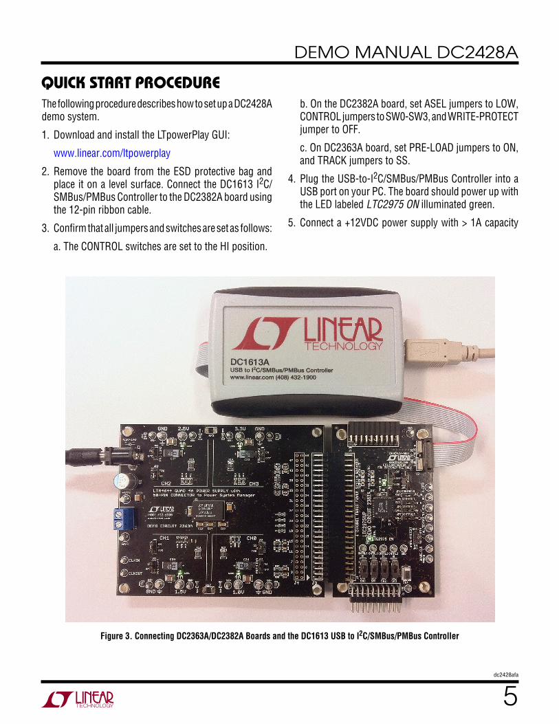
Figure 3. Connecting DC2363A/DC2382A Boards and the DC1613 USB to I2C/SMBus/PMBus Controller
Quick start proceDureThe following procedure describes how to set up a DC2428A demo system.
1. Download and install the LTpowerPlay GUI:
www.linear.com/ltpowerplay
2. Remove the board from the ESD protective bag and place it on a level surface. Connect the DC1613 I2C/SMBus/PMBus Controller to the DC2382A board using the 12-pin ribbon cable.
3. Confirm that all jumpers and switches are set as follows:
a. The CONTROL switches are set to the HI position.
b. On the DC2382A board, set ASEL jumpers to LOW, CONTROL jumpers to SW0-SW3, and WRITE-PROTECT jumper to OFF.
c. On DC2363A board, set PRE-LOAD jumpers to ON, and TRACK jumpers to SS.
4. Plug the USB-to-I2C/SMBus/PMBus Controller into a USB port on your PC. The board should power up with the LED labeled LTC2975 ON illuminated green.
5. Connect a+12VDC power supply with > 1A capacity
6dc2428afa
DEMO MANUAL DC2428A
Quick start proceDureto the VIN input jack of the DC2363A board. The four outputs will power up and the green LEDs will illuminate. The PWR GOOD LED (D6) on the DC2382A board will illuminate.
6. Launch the LTpowerPlay GUI.
a. The GUI automatically identifies the DC2382A and builds a system tree for each I2C device. The system tree on the left hand side will look like this:
b. A green message box will be displayed momentarily in the lower left hand corner confirming that the DC2382A is communicating.
c. You may make configuration changes. When you update registers in the GUI by using either function key F12 to write an individual register or use the Write All icon to write all registers, you may need these settings for future use. Save the demo board configuration to a (*.proj) file by clicking the Save icon. This creates a backup file on your C: drive. Name it whatever you like.
If you need to load the original board default configuration, select the GUI menu pulldown item DEMO > DC2382A_Defaults. This writes the board defaults into the LTC2975’s RAM and automatically to NVM as well.
7. The CONTROL switches are configured to control the channels individually. Slide the switch to HI to enable, GND to disable each channel. To demonstrate chan-nel sequencing, one CONTROL switch may be used to turn all channels on/off. Configuration changes to the LTC2975 are needed. This is covered later in the document.
Loading a Configuration (*.proj) File with the GUI
To load a previously saved proj file:
1. In the upper left hand corner of the GUI, File > Open > browse to your *.proj file. This will load the file into the GUI.
2. Click on the GO ONLINE icon,
then click on the PC RAM icon to write all registers.
This loads the configuration into the working RAM of the LTC2975.
3. To store the configuration to NVM (EEPROM), click on the RAM NVM icon.
7dc2428afa
DEMO MANUAL DC2428A
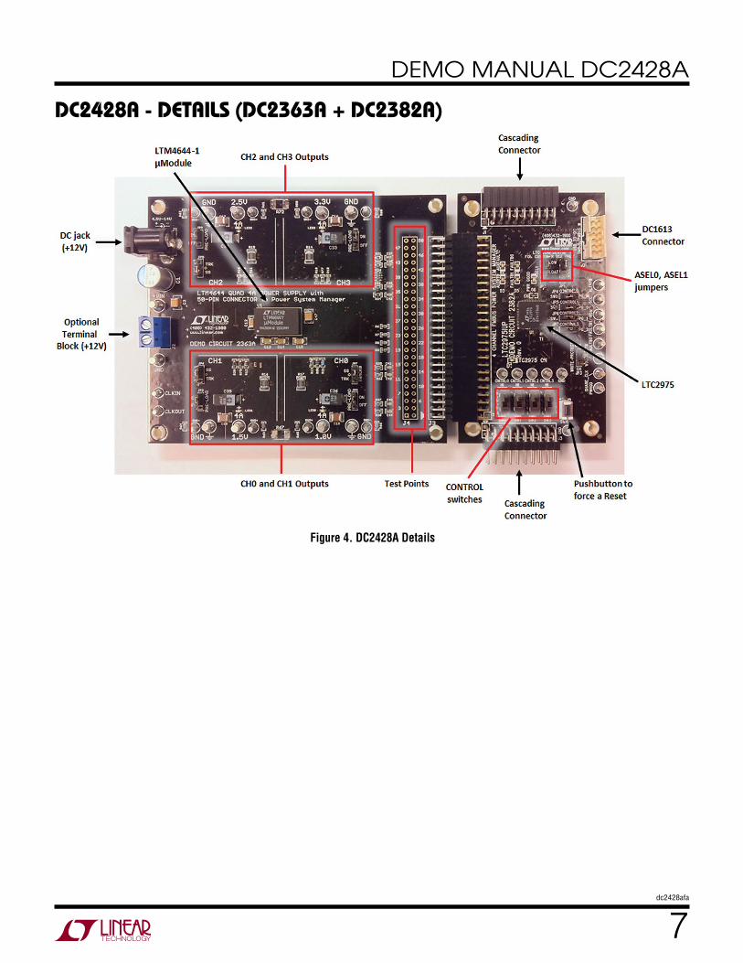
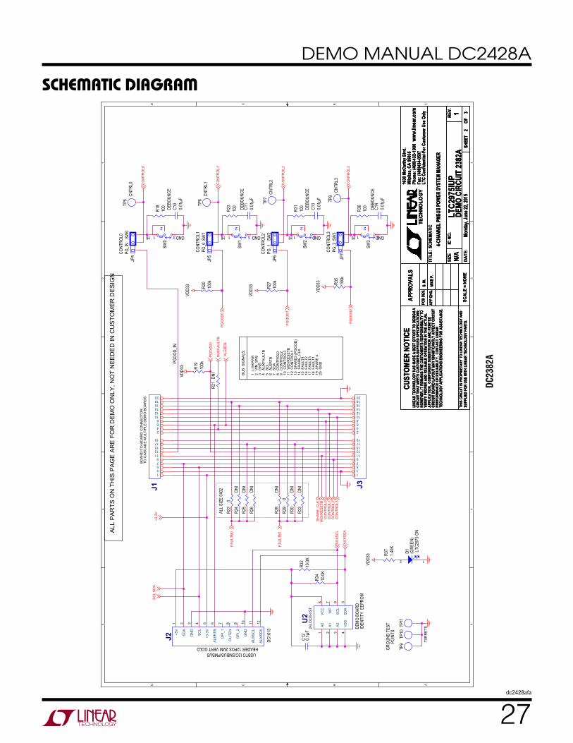
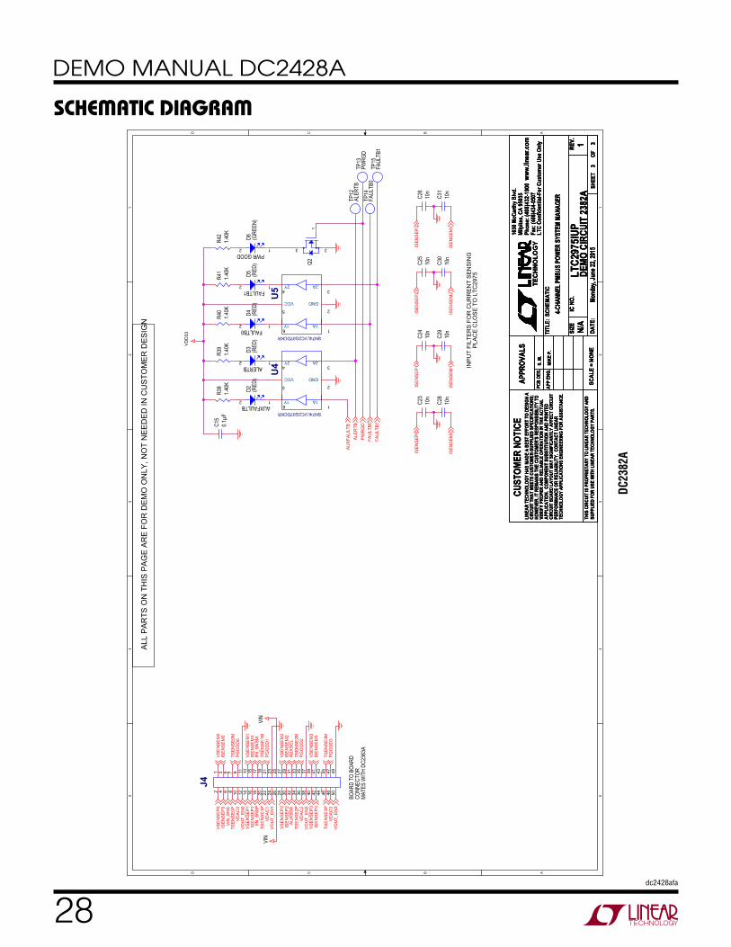
Dc2428a - Details (Dc2363a + Dc2382a)
Figure 4. DC2428A Details
8dc2428afa
DEMO MANUAL DC2428A
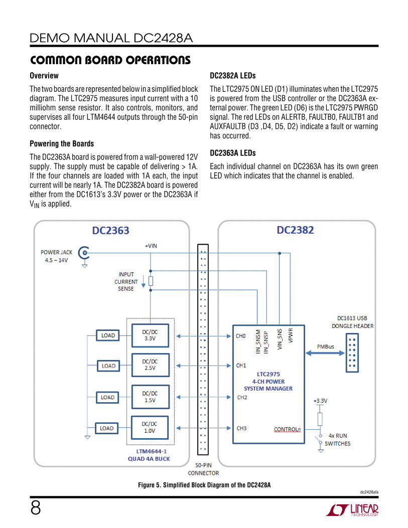
common BoarD operationsOverview
The two boards are represented below in a simplified block diagram. The LTC2975 measures input current with a 10 milliohm sense resistor. It also controls, monitors, and supervises all four LTM4644 outputs through the 50-pin connector.
Powering the Boards
The DC2363A board is powered from a wall-powered 12V supply. The supply must be capable of delivering > 1A. If the four channels are loaded with 1A each, the input current will be nearly 1A. The DC2382A board is powered either from the DC1613’s 3.3V power or the DC2363A if VIN is applied.
Figure 5. Simplified Block Diagram of the DC2428A
DC2382A LEDs
The LTC2975 ON LED (D1) illuminates when the LTC2975 is powered from the USB controller or the DC2363A ex-ternal power. The green LED (D6) is the LTC2975 PWRGD signal. The red LEDs on ALERTB, FAULTB0, FAULTB1 and AUXFAULTB (D3 ,D4, D5, D2) indicate a fault or warning has occurred.
DC2363A LEDs
Each individual channel on DC2363A has its own green LED which indicates that the channel is enabled.
9dc2428afa
DEMO MANUAL DC2428A
common BoarD operationsReset the LTC2975
To reset the LTC2975 and reload the EEPROM contents into operating memory (RAM), press SW4 on the DC2382A.
Pre-Load the Outputs
Each of the outputs on the DC2363A board has a jumper to pre-load the output. When enabled, the load current is pre-defined to be 100mA. This ensures an unloaded output voltage decays to GND quickly when the channel is disabled. This is useful when sequencing off then on quickly.
Controlling/Sequencing Channels
By default the DC2382A board comes with each of the four CTRL switches configured to enable its respective channel.
To demonstrate time-based sequencing, let’s use the CTRL0 switch as the master enable. Select CONTROL0 for each channel as shown. Click the All Paged button and expand the MFR_CONFIG register. Change the controln_sel bit for each channel using in the GUI’s system tree.
The LTC2975 are pre-configured with different TON_DELAY values for each channel. The TON_DELAY parameter is
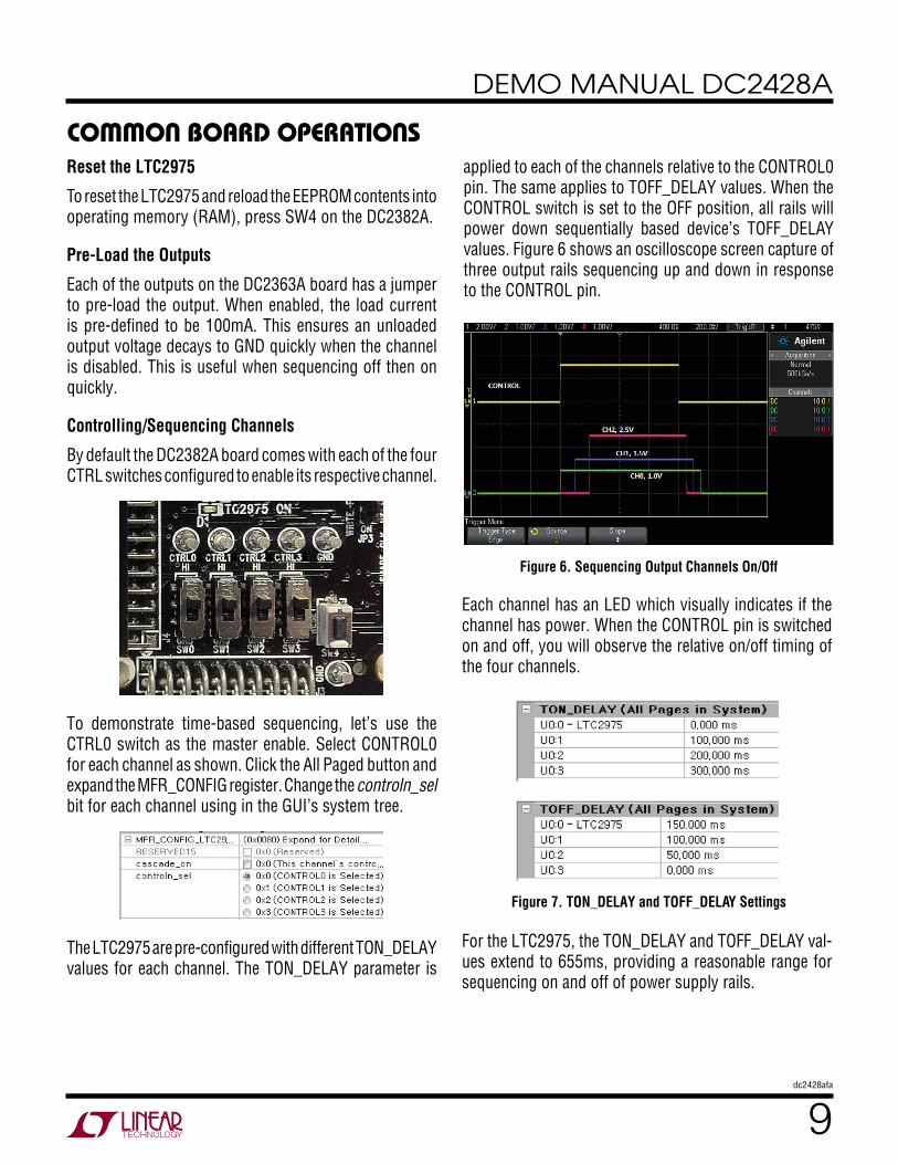
applied to each of the channels relative to the CONTROL0 pin. The same applies to TOFF_DELAY values. When the CONTROL switch is set to the OFF position, all rails will power down sequentially based device’s TOFF_DELAY values. Figure 6 shows an oscilloscope screen capture of three output rails sequencing up and down in response to the CONTROL pin.
Figure 6. Sequencing Output Channels On/Off
Figure 7. TON_DELAY and TOFF_DELAY Settings
Each channel has an LED which visually indicates if the channel has power. When the CONTROL pin is switched on and off, you will observe the relative on/off timing of the four channels.
For the LTC2975, the TON_DELAY and TOFF_DELAY val-ues extend to 655ms, providing a reasonable range for sequencing on and off of power supply rails.
10dc2428afa
DEMO MANUAL DC2428A
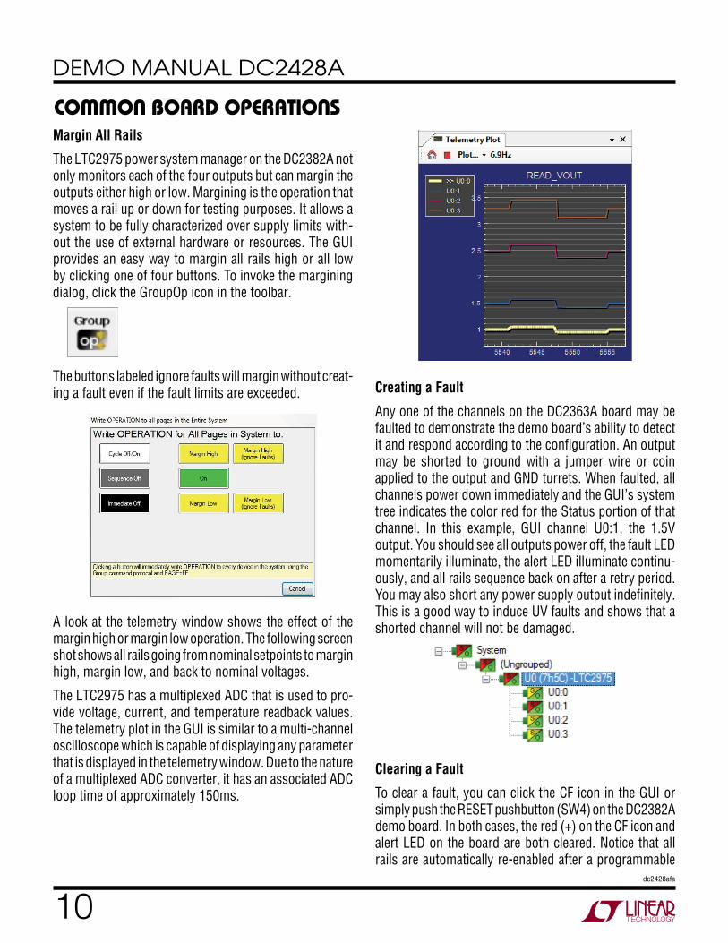
Margin All Rails
The LTC2975 power system manager on the DC2382A not only monitors each of the four outputs but can margin the outputs either high or low. Margining is the operation that moves a rail up or down for testing purposes. It allows a system to be fully characterized over supply limits with-out the use of external hardware or resources. The GUI provides an easy way to margin all rails high or all low by clicking one of four buttons. To invoke the margining dialog, click the GroupOp icon in the toolbar.
The buttons labeled ignore faults will margin without creat-ing a fault even if the fault limits are exceeded.
A look at the telemetry window shows the effect of the margin high or margin low operation. The following screen shot shows all rails going from nominal setpoints to margin high, margin low, and back to nominal voltages.
The LTC2975 has a multiplexed ADC that is used to pro-vide voltage, current, and temperature readback values. The telemetry plot in the GUI is similar to a multi-channel oscilloscope which is capable of displaying any parameter that is displayed in the telemetry window. Due to the nature of a multiplexed ADC converter, it has an associated ADC loop time of approximately 150ms.
common BoarD operations
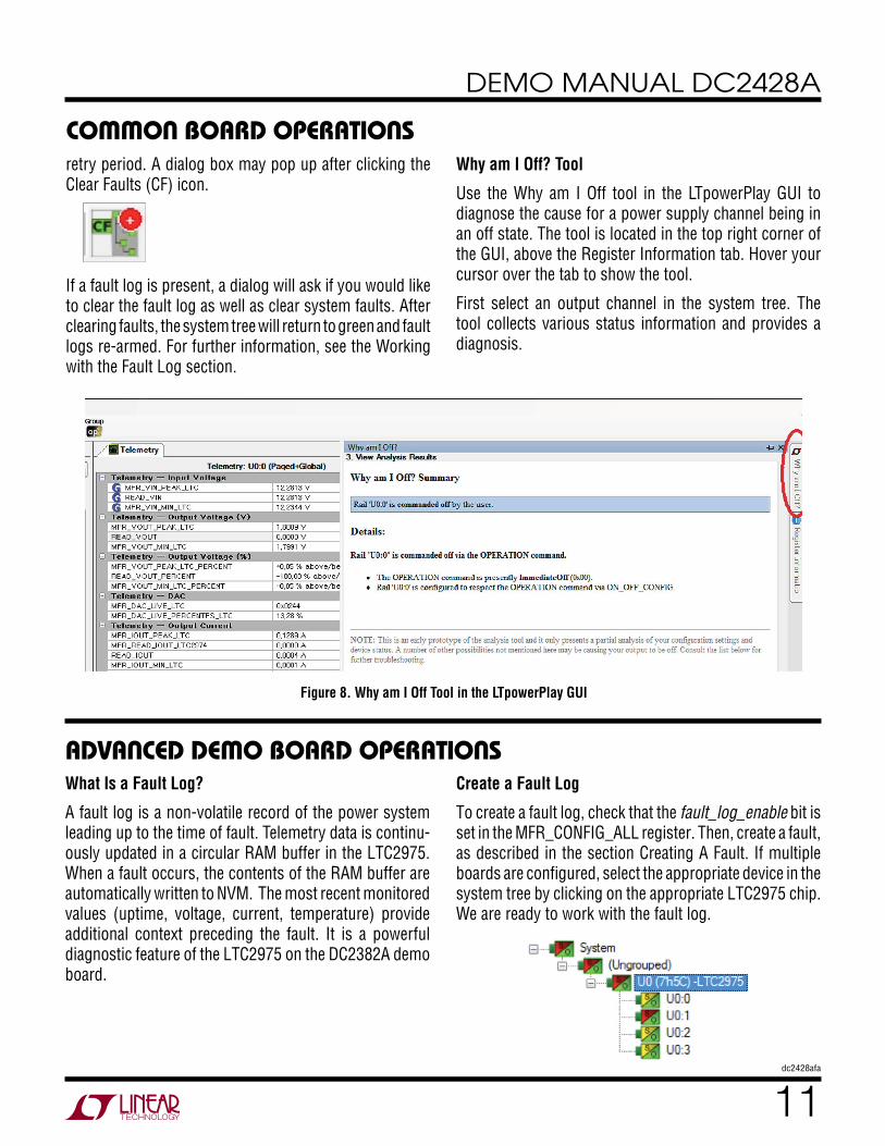
Creating a Fault
Any one of the channels on the DC2363A board may be faulted to demonstrate the demo board’s ability to detect it and respond according to the configuration. An output may be shorted to ground with a jumper wire or coin applied to the output and GND turrets. When faulted, all channels power down immediately and the GUI’s system tree indicates the color red for the Status portion of that channel. In this example, GUI channel U0:1, the 1.5V output. You should see all outputs power off, the fault LED momentarily illuminate, the alert LED illuminate continu-ously, and all rails sequence back on after a retry period. You may also short any power supply output indefinitely. This is a good way to induce UV faults and shows that a shorted channel will not be damaged.
Clearing a Fault
To clear a fault, you can click the CF icon in the GUI or simply push the RESET pushbutton (SW4) on the DC2382A demo board. In both cases, the red(+)on the CF icon and alert LED on the board are both cleared. Notice that all rails are automatically re-enabled after a programmable
11dc2428afa
DEMO MANUAL DC2428A
retry period. A dialog box may pop up after clicking the Clear Faults (CF) icon.
If a fault log is present, a dialog will ask if you would like to clear the fault log as well as clear system faults. After clearing faults, the system tree will return to green and fault logs re-armed. For further information, see the Working with the Fault Log section.
common BoarD operations
aDvanceD Demo BoarD operations
Why am I Off? Tool
Use the Why am I Off tool in the LTpowerPlay GUI to diagnose the cause for a power supply channel being in an off state. The tool is located in the top right corner of the GUI, above the Register Information tab. Hover your cursor over the tab to show the tool.
First select an output channel in the system tree. The tool collects various status information and provides a diagnosis.
Figure 8. Why am I Off Tool in the LTpowerPlay GUI
What Is a Fault Log?
A fault log is a non-volatile record of the power system leading up to the time of fault. Telemetry data is continu-ously updated in a circular RAM buffer in the LTC2975. When a fault occurs, the contents of the RAM buffer are automatically written to NVM. The most recent monitored values (uptime, voltage, current, temperature) provide additional context preceding the fault. It is a powerful diagnostic feature of the LTC2975 on the DC2382A demo board.
Create a Fault Log
To create a fault log, check that the fault_log_enable bit is set in the MFR_CONFIG_ALL register. Then, create a fault, as described in the section Creating A Fault. If multiple boards are configured, select the appropriate device in the system tree by clicking on the appropriate LTC2975 chip. We are ready to work with the fault log.

12dc2428afa
DEMO MANUAL DC2428A
aDvanceD Demo BoarD operationsWorking with the Fault Log
Once a fault has occurred, the Fault Log (FL) icon will show a red(+)sign on it, indicating that the GUI has detected a fault log in the device. Clicking the icon will bring up a dialog box.
Note that it is a context sensitive icon. If multiple DC2382A boards are connected, be sure that the desired device is selected in the system tree.
Once a fault occurs, the device will automatically write the fault log data to EEPROM (NVM). At this point, the log is locked and will not change until it is cleared by the user.
It is a 2-step process to read the fault log. First click the NVM to RAM button. At this point the RAM Log is locked. Click the Read NVM Log button. The log data will appear in the text box below.
The log contains timestamp, up-time, channel voltage readings, an input voltage reading, an on-chip temperature reading, etc. There will be a number of loops; each loop
contains data obtained in one ADC loop time with the most recent ADC loop data on top and the oldest data at the bottom of the log. The up-time indicates, at the time of fault, the amount of time the device had been powered up or time since the previous reset.
In this case, the fault log will show that channel U0:1 faulted due to a VOUT_UV_FAULT condition. On the pre-vious telemetry loop, the channel voltage reading was a nominal value (3.3V). You can save the fault log to a file (.rtf) by clicking the Export button.
To clear the fault log, click the Clear/Rearm EEPROM Log button. This allows the selected device to be ready for a new fault event. To clear all faults, click the Clear Faults (CF) icon.
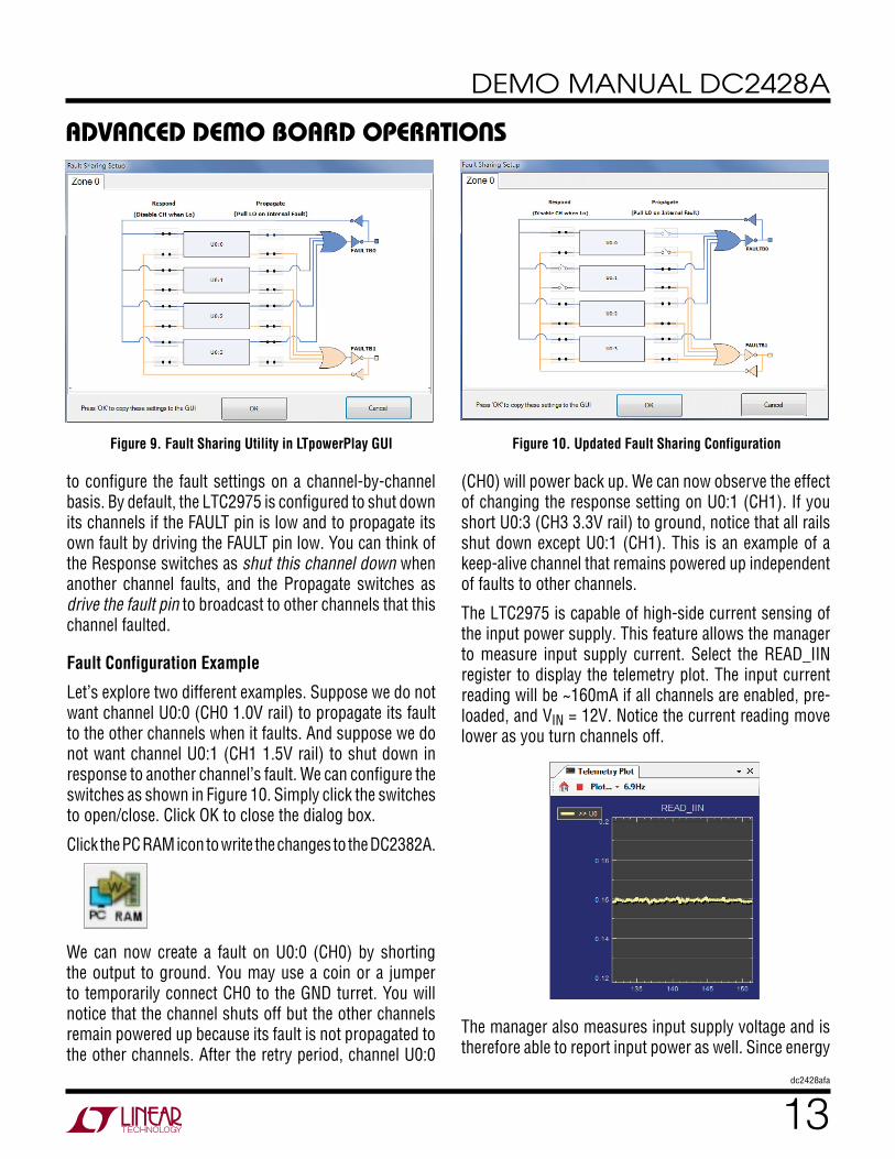
Fault Sharing Setup in the GUI
Fault sharing provides a means of propagating a fault detected by a power manager to other power managers via FAULT pins. Use the Fault Sharing Setup Tool to con-figure the fault sharing in the GUI. Select the LTC2975 in the system tree. Go to Utilities > Fault Sharing Diagram. (For more details on this topic, please refer to the Fault Management section in the data sheet.)
The fault sharing dialog will appear as shown in Figure 9. All Response and all Propagate switches are closed by default. In this configuration, a fault on a channel will shut down not only the faulted channel but all other channels since the Propagate switches are closed.
There are two types of actions to fault conditions: How a channel responds to another channel’s fault and whether a particular channel propagates its fault to other channels. FAULT pins are bi-directional, meaning the device may drive its fault pin low (output) or may respond to the fault pin when another device drives it low (input). Because the two fault pins are separated on the DC2382A, this allows you
13dc2428afa
DEMO MANUAL DC2428A
aDvanceD Demo BoarD operations
Figure 9. Fault Sharing Utility in LTpowerPlay GUI Figure 10. Updated Fault Sharing Configuration
to configure the fault settings on a channel-by-channel basis. By default, the LTC2975 is configured to shut down its channels if the FAULT pin is low and to propagate its own fault by driving the FAULT pin low. You can think of the Response switches as shut this channel down when another channel faults, and the Propagate switches as drive the fault pin to broadcast to other channels that this channel faulted.
Fault Configuration Example
Let’s explore two different examples. Suppose we do not want channel U0:0 (CH0 1.0V rail) to propagate its fault to the other channels when it faults. And suppose we do not want channel U0:1 (CH1 1.5V rail) to shut down in response to another channel’s fault. We can configure the switches as shown in Figure 10. Simply click the switches to open/close. Click OK to close the dialog box.
Click the PC RAM icon to write the changes to the DC2382A.
We can now create a fault on U0:0 (CH0) by shorting the output to ground. You may use a coin or a jumper to temporarily connect CH0 to the GND turret. You will notice that the channel shuts off but the other channels remain powered up because its fault is not propagated to the other channels. After the retry period, channel U0:0
(CH0) will power back up. We can now observe the effect of changing the response setting on U0:1 (CH1). If you short U0:3 (CH3 3.3V rail) to ground, notice that all rails shut down except U0:1 (CH1). This is an example of a keep-alive channel that remains powered up independent of faults to other channels.
The LTC2975 is capable of high-side current sensing of the input power supply. This feature allows the manager to measure input supply current. Select the READ_IIN register to display the telemetry plot. The input current reading will be ~160mA if all channels are enabled, pre-loaded, and VIN = 12V. Notice the current reading move lower as you turn channels off.
The manager also measures input supply voltage and is therefore able to report input power as well. Since energy

14dc2428afa
DEMO MANUAL DC2428A
aDvanceD Demo BoarD operationsis the product of power and time, accumulated energy is provided based on the manager’s internal timebase.
The meter displayed in the upper right hand corner of the GUI provides a number of bits of information. The needle is a real-time indicator of input power and the smaller five dials show the total accumulated energy similar to a home electricity meter. Digital readouts are also provided for convenience.
The DC2363A demo board has power supplies that are capable of high current. The LTC2975 is able to monitor and measure four outputs and its input power supply. LTpowerPlay offers a simple and easy to understand interface that brings together input and output current, voltage, power, and energy readings.
You may also view the input current, input voltage, input power, and input energy together in tabular format. These appear in the telemetry portion of the GUI. The MFR_EIN register holds the accumulated energy value in milliJoules. There is also a total time that the energy accumulator has been active and is shown as the MFR_EIN_TIME register. The GUI will automatically update the displayed SI prefix as the units change from mJ to J to kJ.
To demonstrate the meter readings and register values,
first select the MFR_EIN register to display the energy in the telemetry plot. Turn off channels 2 and 3 by setting those CTRL switches off. You will notice that the slope has changed. The accumulated energy rate is the slope. Energy is still being accumulating but at a lower rate since channels 0 and 1 remain enabled. Note that the input current has changed from about 160mA down to 48mA as seen in the READ_IIN register. The MFR_EIN_WATTS register displays the input power that is being drawn. This register is the product of the READ_VIN and READ_IIN values. Since the input voltage is 12V, the input power is 12V•160mA or 1.92W. You can confirm this by clicking these three registers one by one and view the telemetry window.
The MFR_EIN and MFR_EIN_TIME registers may be reset by right-clicking the MFR_EIN register which displays an option menu to Clear HW Register. It may also be reset by writing the MFR_EIN_CONFIG register.
Changing Nominal Output Voltages
The nominal output voltage of any channel on the DC2363A can be adjusted by changing feedback resistors. There are two external resistors that set the floating voltage, a topside feedback resistor (RTOP) and a bottom feedback resistor (RBOT). Note that these feedback resistors provide compensation for the IR drop of the sense resistor in the output path.
The equation that relates feedback resistors and VOUT is as follows:
VOUT = (RTOP/RBOT+1)•0.6V

15dc2428afa
DEMO MANUAL DC2428A
aDvanceD Demo BoarD operations
Use the LTpowerPlay’s Resistor Selection Tool to calcu-late resistor values and to display the proper DAC range settings. The Resistor Selection Tool refers to R10, R20, and R30. R10 is the bottom feedback resistor, R20 is the
top feedback resistor, and R30 is the DAC resistor. The DC2363 board uses the LTM4644-1 µModule which allows us to use an external sense resistor in the output path to measure output current. The topside feedback resistor RTOP is wired from the output turret, keeping RSENSE inside the feedback loop and minimizes the IR drop of the sense element.
The bottom feedback resistors (RBOT) for each channel are R10-R13. The output trim resolution and range can be adjusted for any output on the DC2363A by simply chang-ing the RDAC resistor value. The DAC resistors (R30) are R18-R21. Table 2 on shows a summary of the feedback resistor values and DAC resistor values.
Figure 11. Output Voltage Set by Feedback Resistors
Figure 12. LTpowerPlay’s Resistor Selection Tool
L1, 1µH
FB
C147µF
VREF = 0.6V
dc2428a F11
VOUT1V
ERRORAMP
LTM4644-1
RBOT90.9k
RLOADRTOP60.4k
ISENSERSENSE
0.01
16dc2428afa
DEMO MANUAL DC2428A
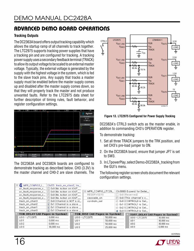
aDvanceD Demo BoarD operationsTracking Outputs
The DC2363A board offers output tracking capability which allows the startup ramp of all channels to track together. The LTC2975 supports tracking power supplies that have a tracking pin and are configured for tracking. A tracking power supply uses a secondary feedback terminal (TRACK) to allow its output voltage to be scaled to an external master voltage. Typically, the external voltage is generated by the supply with the highest voltage in the system, which is fed to the slave track pins. Any supply that tracks a master supply must be enabled before the master supply comes up and disabled after the master supply comes down, so that they will properly track the master and not produce unwanted faults. Refer to the LTC2975 data sheet for further description of timing rules, fault behavior, and register configuration settings.
The DC2363A and DC2382A boards are configured to demonstrate tracking as described below. CH3 (3.3V) is the master channel and CH0-2 are slave channels. The
DC2382A’s CTRL3 switch acts as the master enable, in addition to commanding CH3’s OPERATION register.
To demonstrate tracking:
1. Set all three TRACK jumpers to the TRK position, and set CH3’s pre-load jumper to ON.
2. On the DC2382A board, ensure that jumper JP7 is set to SW3.
3. In LTpowerPlay, select Demo>DC2382A_tracking from the GUI’s menu.
The following register screen shots document the relevant configuration settings.
Figure 13. LTC2975 Configured for Power Supply Tracking
CSS
dc2428a F13
LTM4644-1RUN VOUT3VFBTRACK
19.1k
RUNVFBTRACK
40.2k
RUNVFBTRACK
90.9k
60.4k
60.4k
60.4k
RUNVFBTRACK
LTC2975VOUT_EN3
CTRL3
VDAC3
VOUT_EN2VDAC2
VOUT_EN1VDAC1
VOUT_EN0VDAC0
LOAD
3.3V
VOUT2
LOAD
2.5V
VOUT1
LOAD
1.5V
VOUT0
LOAD
1V

17dc2428afa
DEMO MANUAL DC2428A
aDvanceD Demo BoarD operations
Figure 14. LTC2975 Configured for Cascaded Sequencing
Cascaded Sequencing
The DC2363A/DC2382A board set also offers cascaded sequencing capability. Cascade sequencing allows a master power supply to sequence ON a series of slave supplies by connecting each power supply’s power good output to the control pin of the next power supply in the chain. Note that the power good signal is that of the power supply and not derived from the LTC2975’s internal power good processing. Power good based cascade sequence OFF is not supported. OFF sequencing must be managed using immediate-off or time-based sequencing. A cascade sequence wiring diagram is shown in Figure 14. For each slave channel, the mfr_config_cascade_on bit is set (high) and the associated control input connects to the power good output of the previous power supply. In this configuration each slave channel’s startup is dependent on the previous supply being powered up. The channels cascade on/off via the CTRL0 switch on
the DC2382A board, or command CH0’s OPERATION register on/off. The LTC2975 configuration is such that the controln_sel bit is set to its respective channel. The cascade_on bit is set for the three slave channels (CH1-3) and cleared on the master channel (CH0).
To demonstrate cascade sequencing:
1. Set the three TRACK jumpers to SS on the DC2363A board.
2. Set JP5-JP7 to the PG setting on the DC2382A board.
3. In LTpowerPlay, select Demo>DC2382A_cascade_seq from the GUI’s menu.
dc2428a F14
DC/DC
RUN VOUTP
POWERGOOD0
LTC2975
VOUT_EN0
CONTROL0
FAULT90FAULT90
RECOMMENDEDCONNECTION
WHEN HARDWAREON/OFF CONTROL
IS REQUIRED
CONTROL0
CONTROL1
LOAD MASTER
VSENSP0
VSENSM0VOUTM
DC/DC
RUN VOUTP
POWERGOOD1
VOUT_EN1
CONTROL2
LOAD
SLAVES
TO NEXT CONTROL PIN
VSENSP1
VSENSM1VOUTM
DC/DC
RUN VOUTP
POWERGOOD2
VOUT_EN2
CONTROL3
LOAD
VSENSP2
VSENSM2VOUTM
DC/DC
RUN VOUTP
POWERGOOD3
VOUT_EN3
LOAD
VSENSP3
VSENSM3VOUTM

18dc2428afa
DEMO MANUAL DC2428A
setup proceDure for multi-BoarD arraysMultiple DC2428As can be combined to control as many nine board pairs.
1. Connect DC2363A/DC2382A to pair them.
2. Plug DC2382A’s together.
3. Set a unique address for each DC2382A in the array using ASEL0 and ASEL1 (JP1, JP2). See the following section for further details.
4. Plug the ribbon cable of the DC1613 into one of the DC2382As.
5. Connect a power supply to each of the DC2363A boards. Power is not distributed to other board pairs via the J1/J3 cascading connector.
Figure 15. Array of Multiple Board Sets

19dc2428afa
DEMO MANUAL DC2428A
setup proceDure for multi-BoarD arraysSelecting a Device Address
The DC2382A jumpers (JP1, JP2) are labeled ASEL0 and ASEL1 which allow the user to select one of nine I2C addresses. The I2C/SMBus address of the LTC2975 equals the base address+N where N is a number from 0 to 8. N is configured by setting the ASEL0 and ASEL1 pins to VDD33, GND or FLOAT. See Table 3 below. Using one base address and the nine different values of N, nine LTC2975s can co-exist on the same I2C bus to control 36 outputs. The base address is stored in the MFR_I2C_BASE_ADDRESS register. The base address can be written to any value, but generally should not be changed unless the desired range of addresses overlap existing addresses. Be careful that the address range does not overlap with other I2C/SMBus device or global addresses, including I2C/SMBus multiplexers and bus buffers.
NOTE: Regardless of the jumper setting, the part will always respond to the I2C global 7-bit address 0x5B.
Table 3. Address Selection of LTC2975I2C ADDRESS
(7-BIT)ASEL1
POSITIONASEL0
POSITION DEFAULT
0x5C L L ✓
0x5D L Z
0x5E L H
0x5F Z L
0x60 Z Z
0x61 Z H
0x62 H L
0x63 H Z
0x64 H H
20dc2428afa
DEMO MANUAL DC2428A
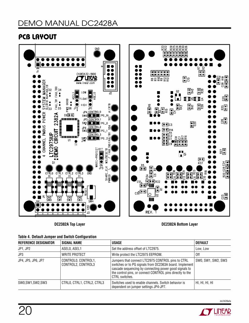
pcB layout
Table 4. Default Jumper and Switch ConfigurationREFERENCE DESIGNATOR SIGNAL NAME USAGE DEFAULT
JP1, JP2 ASEL0, ASEL1 Set the address offset of LTC2975. Low, Low
JP3 WRITE PROTECT Write protect the LTC2975 EEPROM. Off
JP4, JP5, JP6, JP7 CONTROL0, CONTROL1, CONTROL2, CONTROL3
Jumpers that connect LTC2975 CONTROL pins to CTRL switches or to PG signals from DC2363A board. Implement cascade sequencing by connecting power good signals to the control pins, or connect CONTROL pins directly to the CTRL switches.
SW0, SW1, SW2, SW3
SW0,SW1,SW2,SW3 CTRL0, CTRL1, CTRL2, CTRL3 Switches used to enable channels. Switch behavior is dependent on jumper settings JP4-JP7.
HI, HI, HI, HI
DC2382A Top Layer DC2382A Bottom Layer

21dc2428afa
DEMO MANUAL DC2428A
pcB layout
Table 5. Default Jumper SettingsREFERENCE DESIGNATOR SIGNAL NAME USAGE DEFAULT
JP1-JP4 VOUT_CH0, VOUT_CH1, VOUT_CH2, VOUT_CH3
Enable/Disable 100mA pre-load on CH0-CH3 outputs. All On
JP5-JP7 TRACK0, TRACK1, TRACK2 Select Soft-Start (SS) or Tracking feature of Slave Channels (CH0-CH2).
All SS
DC2363A Top Layer

22dc2428afa
DEMO MANUAL DC2428A
pcB layout
DC2363A Bottom Layer
23dc2428afa
DEMO MANUAL DC2428A
Dc2382a parts listITEM QTY REFERENCE PART DESCRIPTION MANUFACTURER/PART NUMBER
Required Circuit Components
1 1 U1 IC 4-CH POWER SYSTEM MANAGER 64QFN LINEAR TECH: LTC2975IUP#PBF
Additional Demo Board Circuit Components
2 9 C1, C2, C3, C4, C6, C8, C9, C12, C15 CAP CERAMIC 0.1µF 16V X7R 0402 AVX: 0402YC104KAT2A
3 6 C5, C10, C11, C13, C14, C20 CAP 0.01µF 25V CERAMIC X7R 0402 AVX: 04023C103KAT2A
4 1 C7 CAP CER 0.1µF 25V X5R 0402 AVX: 04023D104KAT2A
5 8 C23, C24, C25, C26, C28, C29, C30, C31 CAP 2.2nF 16V CERAMIC X7R 0402 AVX: 04023C222KAT2A
6 2 D1, D6 LED GREEN HI-BRT SMD 0603 PANASONIC: LNJ326W83RA
7 4 D2, D3, D4, D5 LED RED SMD 0603 PANASONIC: LNJ237W82RA
8 1 Q1 MOSFET P-CH 20V 200MΩ SOT323-3 ON SEMI: NTS4173PT1G
9 1 Q2 MOSFET N-CH 60V 115MA SOT-23 FAIRCHILD: 2N7002
10 15 R1, R3, R4, R6-R15, R32, R34 RES 10.0k 1/10W 1% 0402 SMD VISHAY: CRCW040210K0FKED
11 5 R2, R18, R23, R31, R36 RES 100Ω 1/10W 1% 0402 SMD VISHAY: CRCW0402100RFKED
12 1 R5 RES 5.49k 1/10W 1% 0402 SMD VISHAY: CRCW04025K49FKED
13 1 R16 RES 150k 1/10W 1% 0402 SMD VISHAY: CRCW0402150KFKED
14 1 R17 RES 49.9k 1/10W 1% 0402 SMD VISHAY: CRCW040249K9FKED
15 4 R19, R20, R27, R35 RES 100k 1/10W 1% 0402 SMD VISHAY: CRCW0402100KFKED
16 7 R21, R24, R25, R26, R28, R30, R33 (OPT) RES 0.0Ω 1/10W 0402 SMD DO NOT INSTALL!
17 2 R22, R29 RES 0.0Ω 1/10W 0402 SMD VISHAY: CRCW04020000Z0ED
18 6 R37, R38, R39, R40, R41, R42 RES 1.4k 1/10W 5% 0402 SMD VISHAY: CRCW04021K40JNED
19 1 U2 IC EEPROM 2KBIT 400Khz 8TSSOP MICROCHIP: 24LC025-I/ST
20 2 U4, U5 IC BUFF/DVR DL NON-INV SC70-6 TEXAS INSTR: SN74LVC2G07DCKR
Hardware: For Demo Board Only
21 1 J1 CONN SOCKET 20POS DUAL ROW MILL MAX 803-43-020-20-001000
22 1 J2 CONN HEADER 12POS 2MM STR DL PCB FCI: 98414-G06-12ULF
23 1 J3 CONN PIN HEADER 20POS DUAL ROW MILL MAX 802-40-020-20-001000
24 1 J4 CONN FEMALE 50POS DL 0.1" R/A GOLD SULLINS: PPPC252LJBN-RC
25 2 JP1, JP2 CONN HEADER 4POS 2MM VERT T/H WURTH: 620 004 111 21
26 5 JP3-JP7 CONN HEADER 3POS 2MM VERT T/H WURTH: 620 003 111 21
27 4 MH1-MH4 SPACER STACKING #4 SCREW NYLON KEYSTONE: 8831
28 4 SW0-SW3 SW SLIDE DPDT 6VDC 0.3A PCMNT C&K: JS202011CQN
29 1 SW4 PUSHBUTTON SWITCH 3.5x6 100GF SMD PANASONIC: EVQ-PJS04K
30 7 SH1-SH7 CONN SHUNT 2MM 2POS BLACK WURTH: 608 002 134 21
31 15 TP1-TP15 TERM SOLDER TURRET 0.156"H 0.084"L MILL MAX: 2308-2-00-80-00-00-07-0
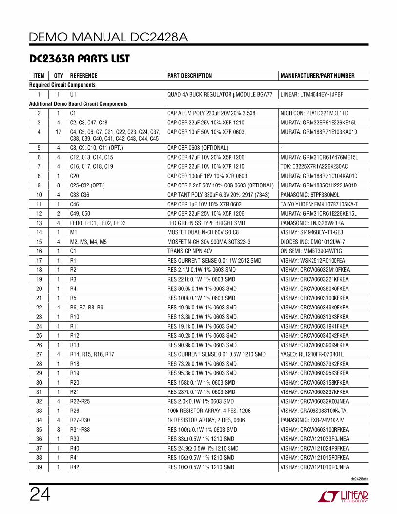
24dc2428afa
DEMO MANUAL DC2428A
Dc2363a parts listITEM QTY REFERENCE PART DESCRIPTION MANUFACTURER/PART NUMBER
Required Circuit Components
1 1 U1 QUAD 4A BUCK REGULATOR µMODULE BGA77 LINEAR: LTM4644EY-1#PBF
Additional Demo Board Circuit Components
2 1 C1 CAP ALUM POLY 220µF 20V 20% 3.5X8 NICHICON: PLV1D221MDL1TD
3 4 C2, C3, C47, C48 CAP CER 22µF 25V 10% X5R 1210 MURATA: GRM32ER61E226KE15L
4 17 C4, C5, C6, C7, C21, C22, C23, C24, C37, C38, C39, C40, C41, C42, C43, C44, C45
CAP CER 10nF 50V 10% X7R 0603 MURATA: GRM188R71E103KA01D
5 4 C8, C9, C10, C11 (OPT.) CAP CER 0603 (OPTIONAL) -
6 4 C12, C13, C14, C15 CAP CER 47µF 10V 20% X5R 1206 MURATA: GRM31CR61A476ME15L
7 4 C16, C17, C18, C19 CAP CER 22µF 10V 10% X7R 1210 TDK: C3225X7R1A226K230AC
8 1 C20 CAP CER 100nF 16V 10% X7R 0603 MURATA: GRM188R71C104KA01D
9 8 C25-C32 (OPT.) CAP CER 2.2nF 50V 10% C0G 0603 (OPTIONAL) MURATA: GRM1885C1H222JA01D
10 4 C33-C36 CAP TANT POLY 330µF 6.3V 20% 2917 (7343) PANASONIC: 6TPF330M9L
11 1 C46 CAP CER 1µF 10V 10% X7R 0603 TAIYO YUDEN: EMK107B7105KA-T
12 2 C49, C50 CAP CER 22µF 25V 10% X5R 1206 MURATA: GRM31CR61E226KE15L
13 4 LED0, LED1, LED2, LED3 LED GREEN SS TYPE BRIGHT SMD PANASONIC: LNJ326W83RA
14 1 M1 MOSFET DUAL N-CH 60V SOIC8 VISHAY: SI4946BEY-T1-GE3
15 4 M2, M3, M4, M5 MOSFET N-CH 30V 900MA SOT323-3 DIODES INC: DMG1012UW-7
16 1 Q1 TRANS GP NPN 40V ON SEMI: MMBT3904WT1G
17 1 R1 RES CURRENT SENSE 0.01 1W 2512 SMD VISHAY: WSK2512R0100FEA
18 1 R2 RES 2.1M 0.1W 1% 0603 SMD VISHAY: CRCW06032M10FKEA
19 1 R3 RES 221k 0.1W 1% 0603 SMD VISHAY: CRCW0603221KFKEA
20 1 R4 RES 80.6k 0.1W 1% 0603 SMD VISHAY: CRCW060380K6FKEA
21 1 R5 RES 100k 0.1W 1% 0603 SMD VISHAY: CRCW0603100KFKEA
22 4 R6, R7, R8, R9 RES 49.9k 0.1W 1% 0603 SMD VISHAY: CRCW060349K9FKEA
23 1 R10 RES 13.3k 0.1W 1% 0603 SMD VISHAY: CRCW060313K3FKEA
24 1 R11 RES 19.1k 0.1W 1% 0603 SMD VISHAY: CRCW060319K1FKEA
25 1 R12 RES 40.2k 0.1W 1% 0603 SMD VISHAY: CRCW060340K2FKEA
26 1 R13 RES 90.9k 0.1W 1% 0603 SMD VISHAY: CRCW060390K9FKEA
27 4 R14, R15, R16, R17 RES CURRENT SENSE 0.01 0.5W 1210 SMD YAGEO: RL1210FR-070R01L
28 1 R18 RES 73.2k 0.1W 1% 0603 SMD VISHAY: CRCW060373K2FKEA
29 1 R19 RES 95.3k 0.1W 1% 0603 SMD VISHAY: CRCW060395K3FKEA
30 1 R20 RES 158k 0.1W 1% 0603 SMD VISHAY: CRCW0603158KFKEA
31 1 R21 RES 237k 0.1W 1% 0603 SMD VISHAY: CRCW0603237KFKEA
32 4 R22-R25 RES 2.0k 0.1W 1% 0603 SMD VISHAY: CRCW06032K00JNEA
33 1 R26 100k RESISTOR ARRAY, 4 RES, 1206 VISHAY: CRA06S083100KJTA
34 4 R27-R30 1k RESISTOR ARRAY, 2 RES, 0606 PANASONIC: EXB-V4V102JV
35 8 R31-R38 RES 100Ω 0.1W 1% 0603 SMD VISHAY: CRCW0603100RFKEA
36 1 R39 RES 33Ω 0.5W 1% 1210 SMD VISHAY: CRCW121033R0JNEA
37 1 R40 RES 24.9Ω 0.5W 1% 1210 SMD VISHAY: CRCW121024R9FKEA
38 1 R41 RES 15Ω 0.5W 1% 1210 SMD VISHAY: CRCW121015R0FKEA
39 1 R42 RES 10Ω 0.5W 1% 1210 SMD VISHAY: CRCW121010R0JNEA

25dc2428afa
DEMO MANUAL DC2428A
Dc2363a parts listITEM QTY REFERENCE PART DESCRIPTION MANUFACTURER/PART NUMBER
40 4 R43-R46 RES 0Ω 0.1W 0603 SMD VISHAY: CRCW06030000Z0EA
41 10 R50, R52, R68-R71, R73-R76 (OPT) RESISTOR (OPTIONAL) VISHAY: CRCW06030000Z0EA
42 3 R53, R55, R57 RES 60.4k 0.1W 1% 0603 SMD VISHAY: CRCW060360K4FKEA
43 1 R54 RES 19.1k 0.1W 1% 0603 SMD VISHAY: CRCW060319K1FKEA
44 1 R56 RES 40.2k 0.1W 1% 0603 SMD VISHAY: CRCW060340K2FKEA
45 1 R58 RES 90.9k 0.1W 1% 0603 SMD VISHAY: CRCW060390K9FKEA
46 8 R59-R66 RES 1.0Ω 0.1W 1% 0603 SMD VISHAY: CRCW06031R00JNEA
47 2 R67, R72 (OPT) RES 0Ω 1W 2010 SMD (OPTIONAL) ROHM: MCR50JZHJ000
48 4 R77-R80 RES 60.4k 0.1W 1% 0603 SMD VISHAY: CRCW060360K4FKEA
49 1 U2 OV/UV SUPPLY PROTECTION CONTROLLER LINEAR: LTC4365ITS8#PBF
50 1 U3 FIXED 3.3V 100mA MICROPOWER LDO LINEAR: LT1761ES5-3.3#PBF
51 1 U4 2KBIT I2C SERIAL EEPROM SOT23-6 MICROCHIP: 24LC025T-I/OT
Hardware: For Demo Board Only
52 1 J1 POWER JACK FROM CUI INC. PJ-002A CUI INC: PJ-002AH
53 1 J2 TERMINAL BLOCK 5mm HORZ ENTRY 2POS WURTH: 691102710002
54 1 J3 CONN HEADER 50POS 0.050 RIGHT ANGLE MOLEX: 90122-0785
55 7 JP1, JP2, JP3, JP4, JP5, JP6, JP7 2MM PIN HEADER 1X3 WURTH: 620 003 111 21
56 1 JP8 4POS DIP SWITCH C&K: TDA04H0SB1R
57 4 MH1-MH4 SPACER STACKING #4 SCREW NYLON KEYSTONE: 8831
58 7 SH1-SH7 CONN SHUNT 2MM 2POS BLACK WURTH: 608 002 134 21
59 10 TP1-TP10 TERM SOLDER TURRET 0.219"H 0.109"L MILL MAX : 2501-2-00-80-00-00-07-0
60 10 TP11, TP12, TP17-TP24 TERM SOLDER TURRET 0.156"H 0.084"L MILL MAX : 2308-2-00-80-00-00-07-0

26dc2428afa
DEMO MANUAL DC2428A
DC23
82A
schematic DiaGram5 5
4 4
3 3
2 2
1 1
DD
CC
BB
AA
WRI
TE-P
ROTE
CT
ONOFF
ASEL
0AS
EL1
HI FLOA
T
LO
HI
FLOA
T
LO
RE
SE
T
NOTE
:TH
E NE
T PU
LLUP
RES
ISTA
NCE
ON S
HARE
_CLK
LINE
SHO
ULD
BE B
ETW
EEN
4.2K
AND
5.5K
NO
TES
- U
NLE
SS
OTH
ER
WIS
E S
PE
CIF
IED
:
NO
TE:
MA
KE
ALL
TS
EN
SE
TR
AC
ES
SH
IELD
ED
AN
D D
IFFE
RE
NTI
AL
PLA
CE
CA
PS
AN
D G
ND
CO
NN
EC
TIO
NS
CA
PS
NE
AR
LTC
2975
1 - A
LL C
HIP
CA
PS
AN
D C
HIP
RE
S A
RE
040
2
VDD3
3
VDD3
3
VDD3
3
VDD3
3
VDD3
3
VDD3
3
VDD3
3
VDD3
3
VDD3
3
VIN
VD
D33
VS
EN
SE
P2
VS
EN
SE
M2
ISE
NS
EP
2IS
EN
SE
M2
VD
AC
2
CO
NTR
OL2
VO
UT_
EN
2
VS
EN
SE
P3
VS
EN
SE
M3
ISE
NS
EP
3IS
EN
SE
M3
VD
AC
3
CO
NTR
OL3
VO
UT_
EN
3
VS
EN
SE
P1
VS
EN
SE
M1
ISE
NS
EP
1IS
EN
SE
M1
VD
AC
1
CO
NTR
OL1
VO
UT_
EN
1
VS
EN
SE
P0
VS
EN
SE
M0
ISE
NS
EP
0IS
EN
SE
M0
VIN
_SN
S
VD
AC
0
CO
NTR
OL0
VO
UT_
EN
0
SH
AR
E_C
LK
ALE
RTB
WD
I/RE
SE
TB
AU
XFA
ULT
B
FAU
LTB
1FA
ULT
B0
TSE
NS
E0P
TSE
NS
E1P
TSE
NS
E2P
TSE
NS
E3P
TSE
NS
E0P
TSE
NS
E0M
TSE
NS
E1P
TSE
NS
E1M
TSE
NS
E2P
TSE
NS
E2M
TSE
NS
E3P
TSE
NS
E3M
PW
RG
D
SC
LS
DA
+3.3
V
IIN_S
NS
MIIN
_SN
SP
REVI
SION
HIS
TORY
DESC
RIPT
ION
DATE
APPR
OVED
ECO
REV
MIC
HAEL
P.
PROT
OTYP
E1
05-1
8-15
__
REVI
SION
HIS
TORY
DESC
RIPT
ION
DATE
APPR
OVED
ECO
REV
MIC
HAEL
P.
PROT
OTYP
E1
05-1
8-15
__
REVI
SION
HIS
TORY
DESC
RIPT
ION
DATE
APPR
OVED
ECO
REV
MIC
HAEL
P.
PROT
OTYP
E1
05-1
8-15
__
SIZE
DATE
:
IC N
O.RE
V.
SHEE
TOF
TITL
E:
APPR
OVAL
S
PCB
DES.
APP
ENG.
TEC
HN
OLO
GY
Fax:
(408
)434
-050
7
Milp
itas,
CA 95
035
Phon
e: (4
08)4
32-1
900
1630
McC
arth
y Blvd
.
LTC
Conf
iden
tial-F
or C
usto
mer
Use
Onl
y
CUST
OMER
NOT
ICE
LINE
AR T
ECHN
OLOG
Y HA
S MA
DE A
BES
T EF
FORT
TO
DESI
GN A
CIRC
UIT
THAT
MEE
TS C
USTO
MER-
SUPP
LIED
SPE
CIFI
CATI
ONS;
HOW
EVER
, IT R
EMAI
NS T
HE C
USTO
MER'
S RE
SPON
SIBI
LITY
TO
VERI
FY P
ROPE
R AN
D RE
LIAB
LE O
PERA
TION
IN T
HE A
CTUA
LAP
PLIC
ATIO
N. C
OMPO
NENT
SUB
STIT
UTIO
N AN
D PR
INTE
DCI
RCUI
T BO
ARD
LAYO
UT M
AY S
IGNI
FICA
NTLY
AFF
ECT
CIRC
UIT
PERF
ORMA
NCE
OR R
ELIA
BILI
TY. C
ONTA
CT L
INEA
RTE
CHNO
LOGY
APP
LICA
TION
S EN
GINE
ERIN
G FO
R AS
SIST
ANCE
.
THIS
CIR
CUIT
IS P
ROPR
IETA
RY T
O LI
NEAR
TEC
HNOL
OGY
AND
SCHE
MAT
IC
SUPP
LIED
FOR
USE
WIT
H LI
NEAR
TEC
HNOL
OGY
PART
S.SC
ALE
= NO
NE
www.
linea
r.com 1
Mond
ay, J
une 2
2, 20
151
3
4-CHA
NNEL
PMBU
S POW
ER SY
STEM
MAN
AGER
S. M
.
MIKE
P.
N/A
LTC2
975I
UPDE
MO C
IRCU
IT 23
82A
R13
10.0K
C4 0.1µF
R14
10.0K
D
G
SQ1 NTS4
173P
T1G
3
1
2
T1
R10
10.0K
JP1
NT4
NET
TIE
R7 10.0K
R2 100
C9 0.1µF
R3 10.0K
R5 5.49K
TP2
SHAR
E_CL
K
R12
10.0K
C3 0.1µF
TP3
SDA
R9 10.0K
TP4
SCL
C60.1
µF
C2 0.1µF
R6 10.0K
JP3
NT2
NET
TIE
TP1
WDI
/RES
ETB
NT1
NET
TIE
R15
10.0K
C7 0.1µF
JP2
C8 0.1µF
R11
10.0K
C20 0.0
1µF
C1 0.1µF
CHANNEL 0CHANNEL 1CHANNEL 2 CHANNEL 3
E-P
AD
U1
LTC
2975
VS
EN
SE
P0
1
VS
EN
SE
M0
2
ISE
NS
EP
041
ISE
NS
EM
042
VIN
_SN
S9
NC
8
TSE
NS
E0
15
CO
NTR
OL0
32
VS
EN
SE
P1
63
VS
EN
SE
M1
64
ISE
NS
EP
143
ISE
NS
EM
144
GN
D60
GN
D59
TSE
NS
E1
16
CO
NTR
OL1
33
VS
EN
SE
P2
61
VS
EN
SE
M2
62
ISE
NS
EP
245
ISE
NS
EM
246
IIN_S
NS
M56
IIN_S
NS
P55
TSE
NS
E2
27
CO
NTR
OL2
22
VS
EN
SE
P3
49
VS
EN
SE
M3
50
ISE
NS
EP
347
ISE
NS
EM
348
GN
D52
VIN
_SN
S_C
AP
51
TSE
NS
E3
34
CO
NTR
OL3
23
VD
AC
053
VD
AC
154
VD
AC
257
VD
AC
358
VO
UT_
EN
03
VO
UT_
EN
14
VO
UT_
EN
25
VO
UT_
EN
36
AU
XFA
ULT
B7
RE
FP38
RE
FM40
VPWR10
VDD3311VDD3312
VDD25(IN)14
VDD25(OUT)13
WP
28
PW
RG
D17
SH
AR
E_C
LK18
SC
L30
SD
A29
ALE
RTB
31
FAU
LTB
025
FAU
LTB
126
AS
EL0
35
AS
EL1
36
GND19
GND20
GND21
GND37
GND39
WD
I/RE
SE
TB24
E-PAD65
R8 10.0K
C5 0.01µ
F
R4 10.0K
SW4
R16
150K
R1 10.0K
NT3
NET
TIE
R17
49.9K
27dc2428afa
DEMO MANUAL DC2428A
DC23
82A
schematic DiaGram5 5
4 4
3 3
2 2
1 1
DD
CC
BB
AA
DC16
13
1 L
GK
PW
R2
VIN
_SN
S3
GN
D4
AU
XFA
ULT
B5
SC
L6
ALE
RTB
7 S
DA
8 C
ON
TRO
L09
CO
NTR
OL2
10 C
ON
TRO
L311
WD
I/RE
SE
TB12
CO
NTR
OL1
13 S
PA
RE
3 (P
GO
OD
)14
SH
AR
E_C
LK15
FA
ULT
416
FA
ULT
217
FA
ULT
318
FA
ULT
119
SP
AR
E 4
20 G
ND
DEMO
BOA
RDID
ENTI
TY E
EPRO
M
HI GND
CONT
ROL1 HI GND
CONT
ROL2 HI GND
CONT
ROL3
BO
AR
D-T
O-B
OA
RD
CO
NN
EC
TOR
TO C
AS
CA
DE
MU
LTIP
LE D
EM
O B
OA
RD
S
DEBO
UNCE
DEBO
UNCE
DEBO
UNCE
ALL
PA
RTS
ON
TH
IS P
AG
E A
RE
FO
R D
EM
O O
NLY
, NO
T N
EE
DE
D IN
CU
STO
ME
R D
ES
IGN
HI GND
CONT
ROL0
DEBO
UNCE
PG_0
PG_1
PG_2
PG_IN
SW1
SW2
SW3
SW0
ALL S
IZE
0402
BU
S S
IGN
ALS
:
USBTO I2C/SMBUS/PMBUS
GROU
ND T
EST
P
OINT
S
PGOO
D_IN
LTC2
975 O
N
VDD3
3
VDD3
3VD
D33
VDD3
3
VDD3
3
SC
LS
DA
AU
XFA
ULT
B
FAU
LTB
1
FAU
LTB
0
CO
NTR
OL2
WD
I/RE
SE
TB
CO
NTR
OL3
ALE
RTB
CO
NTR
OL0
CO
NTR
OL1
PG
OO
D0
PG
OO
D1
PG
OO
D2
SH
AR
E_C
LK
CO
NTR
OL0
CO
NTR
OL1
CO
NTR
OL2
CO
NTR
OL3
PG
OO
D3
AU
XS
CL
AU
XS
DA
+3.3
V
SIZE
DATE
:
IC N
O.RE
V.
SHEE
TOF
TITL
E:
APPR
OVAL
S
PCB
DES.
APP
ENG.
TEC
HN
OLO
GY
Fax:
(408
)434
-050
7
Milp
itas,
CA 95
035
Phon
e: (4
08)4
32-1
900
1630
McC
arth
y Blvd
.
LTC
Conf
iden
tial-F
or C
usto
mer
Use
Onl
y
CUST
OMER
NOT
ICE
LINE
AR T
ECHN
OLOG
Y HA
S MA
DE A
BES
T EF
FORT
TO
DESI
GN A
CIRC
UIT
THAT
MEE
TS C
USTO
MER-
SUPP
LIED
SPE
CIFI
CATI
ONS;
HOW
EVER
, IT R
EMAI
NS T
HE C
USTO
MER'
S RE
SPON
SIBI
LITY
TO
VERI
FY P
ROPE
R AN
D RE
LIAB
LE O
PERA
TION
IN T
HE A
CTUA
LAP
PLIC
ATIO
N. C
OMPO
NENT
SUB
STIT
UTIO
N AN
D PR
INTE
DCI
RCUI
T BO
ARD
LAYO
UT M
AY S
IGNI
FICA
NTLY
AFF
ECT
CIRC
UIT
PERF
ORMA
NCE
OR R
ELIA
BILI
TY. C
ONTA
CT L
INEA
RTE
CHNO
LOGY
APP
LICA
TION
S EN
GINE
ERIN
G FO
R AS
SIST
ANCE
.
THIS
CIR
CUIT
IS P
ROPR
IETA
RY T
O LI
NEAR
TEC
HNOL
OGY
AND
SCHE
MAT
IC
SUPP
LIED
FOR
USE
WIT
H LI
NEAR
TEC
HNOL
OGY
PART
S.SC
ALE
= NO
NE
www.
linea
r.com 1
Mond
ay, J
une 2
2, 20
152
3
4-CHA
NNEL
PMBU
S POW
ER SY
STEM
MAN
AGER
S. M
.
MIKE
P.
N/A
LTC2
975I
UPDE
MO C
IRCU
IT 23
82A
JP4
R19
100k
R22
0
J1
135791113151719
2468101214161820
R27
100k
R24
DNI
R35
100k
C12
0.1µF
C10
0.01µ
F
TP11
J2
HEADER 12POS 2MM VERT GOLD
+5V
1
SD
A2
GN
D3
SC
L4
+3.3
V5
ALE
RTB
6
GP
I_1
7
OU
TEN
8
GP
I_2
9
GN
D10
AU
XS
CL
11
AU
XS
DA
12
JP6
C14
0.01µ
F
TP9
R32
10.0K
TP5
CNTR
L0
1
2
3
SW2
R33
DNI
TP6
CNTR
L1
C13
0.01µ
F
JP7
C11
0.01µ
F
R34
10.0K
R20
100k
R30
DNI
TP7
CNTR
L2
D1 (GRE
EN)
2 1
R21
DNI
R29
0
R25
DNI
R36
100
J3
13579
1113151719
2468
101214161820
1
2
3
SW0
R23
100
R28
DNI
TP8
CNTR
L3
TP10
TUR
RE
TS
R31
100
R18
100
R37
1.40K
R26
DNI
1
2
3
SW3
1
2
3
SW1
JP5
U2
24LC
025-
I/ST
A0
1
A1
2
A2
3
VS
S4
SD
A5
SC
L6
WP
7V
CC
8
28dc2428afa
DEMO MANUAL DC2428A
schematic DiaGram5 5
4 4
3 3
2 2
1 1
DD
CC
BB
AA
ALL
PA
RTS
ON
TH
IS P
AG
E A
RE
FO
R D
EM
O O
NLY
, NO
T N
EE
DE
D IN
CU
STO
ME
R D
ES
IGN
ALERTB
FAULTB1
FAULTB0
AUXFAULTB
PWR GOOD
BOAR
D TO
BOA
RDCO
NNEC
TOR
MATE
S W
ITH
DC23
63A
INP
UT
FILT
ER
S F
OR
CU
RR
EN
T S
EN
SIN
G
P
LAC
E C
LOS
E T
O L
TC29
75
VD
D33
VIN
VIN
AU
XFA
ULT
B
FAU
LTB
1
PW
RG
DFA
ULT
B0
ALE
RTB
ISE
NS
EP
0
ISE
NS
EM
0
ISE
NS
EP
1
ISE
NS
EM
1
ISE
NS
EP
2
ISE
NS
EM
2
ISE
NS
EP
3
ISE
NS
EM
3
AU
XS
DA
AU
XS
CL
PG
OO
D0
PG
OO
D1
VS
EN
SE
P1
ISE
NS
EP
1V
SE
NS
EM
1IS
EN
SE
M1
VO
UT_
EN
1
TSE
NS
E1P
TSE
NS
E1M
VS
EN
SE
P3
ISE
NS
EP
3V
SE
NS
EM
3IS
EN
SE
M3
TSE
NS
E3M
TSE
NS
E3P
VO
UT_
EN
3V
DA
C3
VS
EN
SE
P2
PG
OO
D2
ISE
NS
EP
2V
SE
NS
EM
2IS
EN
SE
M2
TSE
NS
E2M
TSE
NS
E2P
VO
UT_
EN
2V
DA
C2
VS
EN
SE
P0
VS
EN
SE
M0
ISE
NS
EP
0IS
EN
SE
M0
VIN
_SN
S
VD
AC
0V
OU
T_E
N0
TSE
NS
E0P
TSE
NS
E0M
VD
AC
1
PG
OO
D3
IIN_S
NS
PIIN
_SN
SM
SIZE
DATE
:
IC N
O.RE
V.
SHEE
TOF
TITL
E:
APPR
OVAL
S
PCB
DES.
APP
ENG.
TEC
HN
OLO
GY
Fax:
(408
)434
-050
7
Milp
itas,
CA 95
035
Phon
e: (4
08)4
32-1
900
1630
McC
arth
y Blvd
.
LTC
Conf
iden
tial-F
or C
usto
mer
Use
Onl
y
CUST
OMER
NOT
ICE
LINE
AR T
ECHN
OLOG
Y HA
S MA
DE A
BES
T EF
FORT
TO
DESI
GN A
CIRC
UIT
THAT
MEE
TS C
USTO
MER-
SUPP
LIED
SPE
CIFI
CATI
ONS;
HOW
EVER
, IT R
EMAI
NS T
HE C
USTO
MER'
S RE
SPON
SIBI
LITY
TO
VERI
FY P
ROPE
R AN
D RE
LIAB
LE O
PERA
TION
IN T
HE A
CTUA
LAP
PLIC
ATIO
N. C
OMPO
NENT
SUB
STIT
UTIO
N AN
D PR
INTE
DCI
RCUI
T BO
ARD
LAYO
UT M
AY S
IGNI
FICA
NTLY
AFF
ECT
CIRC
UIT
PERF
ORMA
NCE
OR R
ELIA
BILI
TY. C
ONTA
CT L
INEA
RTE
CHNO
LOGY
APP
LICA
TION
S EN
GINE
ERIN
G FO
R AS
SIST
ANCE
.
THIS
CIR
CUIT
IS P
ROPR
IETA
RY T
O LI
NEAR
TEC
HNOL
OGY
AND
SCHE
MAT
IC
SUPP
LIED
FOR
USE
WIT
H LI
NEAR
TEC
HNOL
OGY
PART
S.SC
ALE
= NO
NE
www.
linea
r.com 1
Mond
ay, J
une 2
2, 20
153
3
4-CHA
NNEL
PMBU
S POW
ER SY
STEM
MAN
AGER
S. M
.
MIKE
P.
N/A
LTC2
975I
UPDE
MO C
IRCU
IT 23
82A
C30
10n
D4 (RED
)
2 1
C26
10n
R41
1.40K
U4
SN74LVC2G07DCKR
1A1
GND
2
2A3
2Y4
VCC
5
1Y6
Q2
3
1
2
TP15
FAUL
TB1
C24
10n
R40
1.40K
D5 (RED
)
2 1
R39
1.40K
R38
1.40K
D6 (GRE
EN)
2 1
C28
10n
J41 3 5 7 9 11 13 15 17 19 21 23 25 27 29
2 4 6 8 10 12 14 16 18 20 22 24 26 28 30 32 34 36 38 40 42 44 46 48 50
31 33 35 37 39 41 43 45 47 49
U5
SN74LVC2G07DCKR
1A1
GND
2
2A3
2Y4
VCC
5
1Y6
TP13
PWRG
D
C31
10n
C25
10n
D2 (RED
)
2 1
C29
10n
C23
10n
D3 (RED
)
2 1
R42
1.40K
TP12
ALER
TB
C15
0.1µF
TP14
FAUL
TB0
DC23
82A

29dc2428afa
DEMO MANUAL DC2428A
schematic DiaGram
DC23
63A
VIN
_S
NS
VO
UT
_C
H3
VO
UT
_C
H2
VO
UT
_C
H1
VO
UT
_C
H0
LT
M4
64
4-1
LT
M4
64
4-1
Qu
ad
4A
Su
pp
ly
MT
P
MT
P
1b
Input P
rote
ction
Quad 4
A D
C/D
C C
onvert
er
(OV
/UV
/Revers
e)
+3.3
V
+2.5
V
+1.5
V
+1.0
V
+V
IN
GN
D
with
50
-pin
Co
nn
ecto
r to
Po
we
r S
yste
m M
an
ag
er
De
mo
Circu
it 2
36
3A
DC
M
CC
MO
PE
RA
TIO
NM
OD
E
4x 2
2uF
/25V
GN
D
10n
10
m
GN
D
LT
M4
64
4-1
GN
D
22uF
/25V
LT
C4
36
5
22
1k
80
.6k
GN
DG
ND
2.1
M1
00
k
69
11
02
71
00
02
GN
D
22
0u
F/2
0V
GN
D
13
.3k
19
.1k
40
.2k
90
.9k
22uF
/25V
OP
T
OP
T
OP
T
OP
T
GN
D
GN
D
GN
D
73
.2k
95
.3k
15
8k
23
7k
10
m
10
m
10
m
10
m
49
.9k
49
.9k
49
.9k
49
.9k
47uF
/10V
47uF
/10V
47uF
/10V
47uF
/10V
22uF
/10V
22uF
/10V
22uF
/10V
22uF
/10V
100n
10k
10k
10k
10k
GN
D
TE
MP
SE
NS
E
OP
T
GN
D
60
.4k
60
.4k
60
.4k
60
.4k
33
0u
F
33
0u
F
33
0u
F
33
0u
F
TD
A0
4H
0S
K1
AG
ND
AG
ND
AG
ND
AG
ND
AG
ND
GN
DG
ND
GN
D
GN
D
GN
D
OP
T
GN
DG
ND
GN
D
AG
ND
1 3 2
C4
R1
B4
E4
H4
L4
C6
F6
J6
K7
F3
F7
A4*21
A1*3
A7
A6
C1*3
D7
D6
F1*3
G7
G6
J1*3
J7
K6
B3
E3
H3
L3
B5
C4
B6
E5
F4
E6
H5
J4
H6
L5
K5
L6
B7
E7
H7
L7
C3
C2
F2
J2
C7
J3
U1
C2
SI4
946B
EY
M1
VIN
1
SH
DN
5
UV
2
OV
3
GND4
/FA
ULT
6
VO
UT
7
GATE8
U2
R3
R4
R2
R5
12J2
C1
R1
0
R11
R1
2
R1
3
C3
C8
C10
C9
C11
R1
8
R1
9
R2
0
R2
1
R1
4
R1
5
R1
6
R1
7
R6
R7
R8
R9
C12
C13
C14
C15
C16 C17
C18
C19
C20
R43
R44
R45
R46
Q1
R5
2
C47
R7
7
R7
8
R7
9
R8
0
C3
3
C3
4
C3
5
C3
6
5
6
7
81
2
3
4
JP
8
R5
0
C48
C49
C50
GN
D
GN
D
GN
D
GN
D
VIN
TS
EN
SE
0P
TR
AC
K3
IIN
_S
NS
P
IIN
_S
NS
M
CL
KIN
CL
KO
UT
3P
3V
RU
N_
CH
3
RU
N_
CH
2
RU
N_
CH
1
RU
N_
CH
0
ISP
3
ISM
3
VD
AC
3
ISP
2
ISM
2
VD
AC
2
ISP
1
ISM
1
VD
AC
1
ISP
0
ISM
0
VD
AC
0
TR
AC
K2
TR
AC
K1
TR
AC
K0
PG
3
PG
2
PG
1
PG
0
11
-28
-16
M P
ete
rsP
rod
uctio
n1
b
CU
ST
OM
ER
NO
TIC
E
BS
CA
LE
= N
ON
E
LTC
CO
NF
IDE
NT
IAL
FO
R C
US
TO
ME
RU
SE
ON
LYP
CB
DE
S.
AP
P E
NG
.w
ww
.lin
ear.
com
-
VIN
1
VIN
2
VIN
3
VIN
4
RU
N1
RU
N2
RU
N3
RU
N4
VO
UT
1
VO
UT
2
VO
UT
3
VO
UT
4
FB
1
FB
2
FB
3
FB
4
TR
AC
K/S
S1
TR
AC
K/S
S2
TR
AC
K/S
S3
TR
AC
K/S
S4
TEMP
SGND
GND
VIN
1
VIN
2
VIN
3
VIN
4
SV
IN1
INT
VC
C1
MO
DE
1
SV
IN2
INT
VC
C2
MO
DE
2
SV
IN3
INT
VC
C3
MO
DE
3
SV
IN4
INT
VC
C4
MO
DE
4
CO
MP
1
CO
MP
2
CO
MP
3
CO
MP
4
PG1PG2PG3PG4
CL
KIN
CL
KO
UT
S1
G1
D2
S2
G2
D1
12
34
ON

30dc2428afa
DEMO MANUAL DC2428A
schematic DiaGram
10
0k
VIN
_S
NS
2x1K
2x1K
2x1K
2x1K
LE
D I
nd
ica
tio
nC
urr
en
t S
en
se
Filt
erin
g
Vo
lta
ge
Se
nse
Filt
erin
g
Bo
ard
-to
-Bo
ard
Co
nn
ecto
r
MT
P
MT
P
1a
Te
st
Po
ints
/ O
ptio
na
l H
ea
de
r
VIN
_S
NS
VO
UT
_C
H3
VO
UT
_C
H2
VO
UT
_C
H1
VO
UT
_C
H0
SN
S+
SN
S+
SN
S+
SN
S+
SN
S-
SN
S-
SN
S-
SN
S-
NO
TE
: R
EM
OV
E R
59-R
66 F
OR
RE
MO
TE
SE
NS
ING
LT
M4
64
4 Q
ua
d 4
A S
up
ply
with
50
-pin
Co
nn
ecto
r to
Po
we
r S
yste
m M
an
ag
er
LT
M4
64
4
De
mo
Circu
it 2
36
3A
21
21
21
21
CO
NN
_2
X2
5_
MA
LE
2k
2k
2k
2k
GN
D
R_A
RR
AY
_4X
_C
RA
06S
DM
G1
01
2D
MG
10
12
DM
G1
01
2D
MG
10
12
OP
TO
PT
GN
D
GN
D
OP
TO
PT
GN
D
OP
TO
PT
GN
D
OP
TO
PT
GN
D
10
0
10
010n
10n
GN
D
10
0
10
010n
10n
GN
D
10
0
10
010n
10n
GN
D
10
0
10
010n
10n
GN
D
GN
D
1 1 1 1 1 1 1 1
R_A
RR
AY
_2X
_A
CA
S0606
R_A
RR
AY
_2X
_A
CA
S0606
10n
10n
10n
10n
J3
135
246
79
810
11
13
15
12
14
16
17
19
18
20
21
23
25
22
24
26
27
29
28
30
31
33
32
34
36
38
40
35
37
39
41
42
43
44
45
46
47
48
49
50
R2
2R
23
R2
4R
25
LE
D3
LE
D2
LE
D1
LE
D0
R26
M2
3 2
1
M3
3 2
1
M4
3 2
1
M5
3 2
1
C25
C26
C27
C28
C29
C30
C31
C32
R3
1
R3
2C
37
C38
R3
3
R3
4C
39
C40
R3
5
R3
6C
41
C42
R3
7
R3
8C
43
C44
135
246
79
810
11
13
15
12
14
16
17
19
18
20
21
23
25
22
24
26
27
29
28
30
31
33
32
34
36
38
40
35
37
39
41
42
43
44
45
46
47
48
49
50
J4
R5
9
R6
0
R6
1
R6
2
R6
3
R6
4
R6
5
R6
6
R27
1 234
R28
1 234
123 4
R29
123 4
R30
C21
C22
C23
C24
IIN
_S
NS
M
IIN
_S
NS
M
IIN
_S
NS
P
IIN
_S
NS
P
RU
N_
CH
0
RU
N_
CH
0
RU
N_
CH
2
RU
N_
CH
2
TS
EN
SE
0P
TS
EN
SE
0P
INT
1IN
T2
INT
3IN
T4
GN
D
GN
D
GN
D
GN
D
PG
0
PG
0
PG
0
PG
3
PG
3
PG
3
VIN
VIN
VIN
VIN
VD
AC
1
VD
AC
1
VD
AC
0
VD
AC
0
VD
AC
3
VD
AC
3
VD
AC
2
VD
AC
2
ISM
0
ISM
1
ISM
2
ISM
3
ISN
SP
_C
H3
ISN
SP
_C
H3
ISN
SP
_C
H3
ISN
SM
_C
H3
ISN
SM
_C
H3
ISN
SM
_C
H3
ISN
SP
_C
H2
ISN
SP
_C
H2
ISN
SP
_C
H2
ISN
SM
_C
H2
ISN
SM
_C
H2
ISN
SM
_C
H2
ISN
SP
_C
H1
ISN
SP
_C
H1
ISN
SP
_C
H1
ISN
SM
_C
H1
ISN
SM
_C
H1
ISN
SM
_C
H1
VS
NS
M_
CH
2
VS
NS
M_
CH
2
VS
NS
M_C
H2
VS
NS
P_
CH
2
VS
NS
P_
CH
2
VS
NS
P_C
H2
RU
N_
CH
1
RU
N_
CH
1
RU
N_
CH
3
RU
N_
CH
3
PG
1
PG
1
PG
1
PG
2
PG
2
PG
2
VS
NS
P_
CH
0
VS
NS
P_
CH
0
VS
NS
P_C
H0
VS
NS
M_
CH
0
VS
NS
M_
CH
0
VS
NS
M_C
H0
ISN
SM
_C
H0
ISN
SM
_C
H0
ISN
SM
_C
H0
ISN
SP
_C
H0
ISN
SP
_C
H0
ISN
SP
_C
H0
VS
NS
P_
CH
1
VS
NS
P_
CH
1
VS
NS
P_C
H1
VS
NS
M_
CH
1
VS
NS
M_
CH
1
VS
NS
M_C
H1
VS
NS
P_
CH
3
VS
NS
P_
CH
3
VS
NS
P_C
H3
VS
NS
M_
CH
3
VS
NS
M_
CH
3V
SN
SM
_C
H3
AU
X_
SC
L
AU
X_
SC
L
AU
X_
SD
A
AU
X_
SD
A
ISP
3
ISP
2
ISP
0
ISP
1
05
-12
-15
M P
ete
rsP
rod
uctio
n1
a
CU
ST
OM
ER
NO
TIC
E
BS
CA
LE
= N
ON
E
LTC
CO
NF
IDE
NT
IAL
FO
R C
US
TO
ME
RU
SE
ON
LYP
CB
DE
S.
AP
P E
NG
.w
ww
.lin
ear.
com
-
DC23
63A
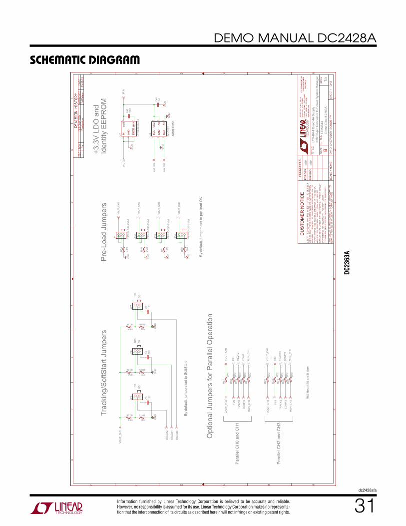
31dc2428afa
DEMO MANUAL DC2428A
Information furnished by Linear Technology Corporation is believed to be accurate and reliable. However, no responsibility is assumed for its use. Linear Technology Corporation makes no representa-tion that the interconnection of its circuits as described herein will not infringe on existing patent rights.
schematic DiaGram
Ide
ntity
EE
PR
OM
Pre
-Lo
ad
Ju
mp
ers
VO
UT
_C
H3
VO
UT
_C
H2
VO
UT
_C
H1
VO
UT
_C
H0
Tra
ckin
g/S
oft
Sta
rt J
um
pe
rs
VO
UT
_C
H3
TR
K
SS
TR
K
SS
TR
K
SS
LT
M4
64
4 Q
ua
d 4
A S
up
ply
with
50
-pin
Co
nn
ecto
r to
Po
we
r S
yste
m M
an
ag
er
Op
tio
na
l Ju
mp
ers
fo
r P
ara
llel O
pe
ratio
n
FB
0F
B1
TR
AC
K1
CO
MP
1
RU
N_
CH
1
TR
AC
K0
CO
MP
0
RU
N_
CH
0
VO
UT
_C
H0
VO
UT
_C
H2
VO
UT
_C
H3
VO
UT
_C
H1
FB
2F
B3
TR
AC
K3
CO
MP
3
RU
N_
CH
3
TR
AC
K2
CO
MP
2
RU
N_
CH
2
Pa
ralle
l C
H0
an
d C
H1
Pa
ralle
l C
H2
an
d C
H3
LT
M4
64
4
De
mo
Circu
it 2
36
3A
R6
7 th
ru R
76
are
0 o
hm
Addr
0x51
1a
MT
P
MT
P
By d
efa
ult, ju
mpers
set to
SoftS
tart
By d
efa
ult, ju
mpers
set to
pre
-load O
N
+3
.3V
LD
O a
nd
24
LC
02
5
LT
17
61
ES
5-3
.3
GN
D
GN
D10nF
1uF
GN
D
PIN
HD
-1X
3-2
MM
PIN
HD
-1X
3-2
MM
PIN
HD
-1X
3-2
MM
PIN
HD
-1X
3-2
MM
33
R
25
R
15
R
10
RG
ND
GN
D
GN
D
GN
D
60.4k 19.1k
60.4k 40.2k
60.4k 90.9k
GN
DG
ND
GN
D
10n
10n
10n
DN
I
DN
I
DN
I
DN
I
DN
I
DN
I
DN
I
DN
I
DN
I
DN
I
GN
D
U4
1 2 3456
1 2 345
U3
C45
C46
JP
11 2 3
JP
21 2 3
JP
31 2 3
JP
41 2 3
R3
9
R4
0
R4
1
R4
2
R53 R54
R55 R56
R57 R58
1 2 3
JP
51 2 3
JP
61 2 3
JP
7
C5
C6
C7
R6
7
R7
2
R6
8
R6
9
R7
0
R7
1
R7
3
R7
4
R7
5
R7
6
AU
X_
SD
A
AU
X_
SC
L
3P
3V
VIN
TR
AC
K1
TR
AC
K0
TR
AC
K2
05
-12
-15
M P
ete
rsP
rod
uctio
n1
a
CU
ST
OM
ER
NO
TIC
E
BS
CA
LE
= N
ON
E
LTC
CO
NF
IDE
NT
IAL
FO
R C
US
TO
ME
RU
SE
ON
LYP
CB
DE
S.
AP
P E
NG
.w
ww
.lin
ear.
com
-
SC
L
GN
D
SD
A
VC
C A0
A1
IN GN
D
SH
DN
BY
P
OU
T
DC23
63A

32dc2428afa
DEMO MANUAL DC2428A
Linear Technology Corporation1630 McCarthy Blvd., Milpitas, CA 95035-7417 (408) 432-1900 ● FAX: (408) 434-0507 ● www.linear.com LINEAR TECHNOLOGY CORPORATION 2015
LT 0217 REV A • PRINTED IN USA
DEMONSTRATION BOARD IMPORTANT NOTICE
Linear Technology Corporation (LTC) provides the enclosed product(s) under the following AS IS conditions:
This demonstration board (DEMO BOARD) kit being sold or provided by Linear Technology is intended for use for ENGINEERING DEVELOPMENT OR EVALUATION PURPOSES ONLY and is not provided by LTC for commercial use. As such, the DEMO BOARD herein may not be complete in terms of required design-, marketing-, and/or manufacturing-related protective considerations, including but not limited to product safety measures typically found in finished commercial goods. As a prototype, this product does not fall within the scope of the European Union directive on electromagnetic compatibility and therefore may or may not meet the technical requirements of the directive, or other regulations.
If this evaluation kit does not meet the specifications recited in the DEMO BOARD manual the kit may be returned within 30 days from the date of delivery for a full refund. THE FOREGOING WARRANTY IS THE EXCLUSIVE WARRANTY MADE BY THE SELLER TO BUYER AND IS IN LIEU OF ALL OTHER WARRANTIES, EXPRESSED, IMPLIED, OR STATUTORY, INCLUDING ANY WARRANTY OF MERCHANTABILITY OR FITNESS FOR ANY PARTICULAR PURPOSE. EXCEPT TO THE EXTENT OF THIS INDEMNITY, NEITHER PARTY SHALL BE LIABLE TO THE OTHER FOR ANY INDIRECT, SPECIAL, INCIDENTAL, OR CONSEQUENTIAL DAMAGES.
The user assumes all responsibility and liability for proper and safe handling of the goods. Further, the user releases LTC from all claims arising from the handling or use of the goods. Due to the open construction of the product, it is the user’s responsibility to take any and all appropriate precautions with regard to electrostatic discharge. Also be aware that the products herein may not be regulatory compliant or agency certified (FCC, UL, CE, etc.).
No License is granted under any patent right or other intellectual property whatsoever. LTC assumes no liability for applications assistance, customer product design, software performance, or infringement of patents or any other intellectual property rights of any kind.
LTC currently services a variety of customers for products around the world, and therefore this transaction is not exclusive.
Please read the DEMO BOARD manual prior to handling the product. Persons handling this product must have electronics training and observe good laboratory practice standards. Common sense is encouraged.
This notice contains important safety information about temperatures and voltages. For further safety concerns, please contact a LTC applica-tion engineer.
Mailing Address:
Linear Technology
1630 McCarthy Blvd.
Milpitas, CA 95035
Copyright © 2004, Linear Technology Corporation