dc2227a - lt3669-2 io-link device with multiple … · runs on an atmel atmega microcontroller...
TRANSCRIPT
1dc2227af
DEMO MANUAL DC2227A
Description
LT3669-2IO-Link Device with Multiple Sensors
Demonstration circuit 2227A is a complete IO-Link® de-vice built using the LT®3669-2 to implement an IO-Link v1.1 physical interface (PHY). The IO-Link stack protocol runs on an Atmel ATmega microcontroller which connects to LT3669-2’s logic IO-signals to communicate with an IO-Link master via the CQ1 transceiver.
An LTC2997 temperature sensor, an opto-coupler (light barrier) and a pushbutton demonstrate IO-Link device functionality and master-slave interoperability.
L, LT, LTC, LTM, Linear Technology and the Linear logo are registered trademarks of Linear Technology Corporation. IO-Link is a registered trademark of PROFIBUS User Organization (PNO). All other trademarks are the property of their respective owners.
performance summary
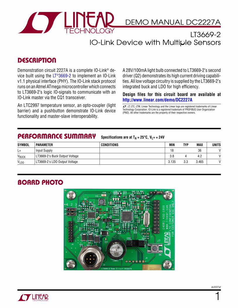
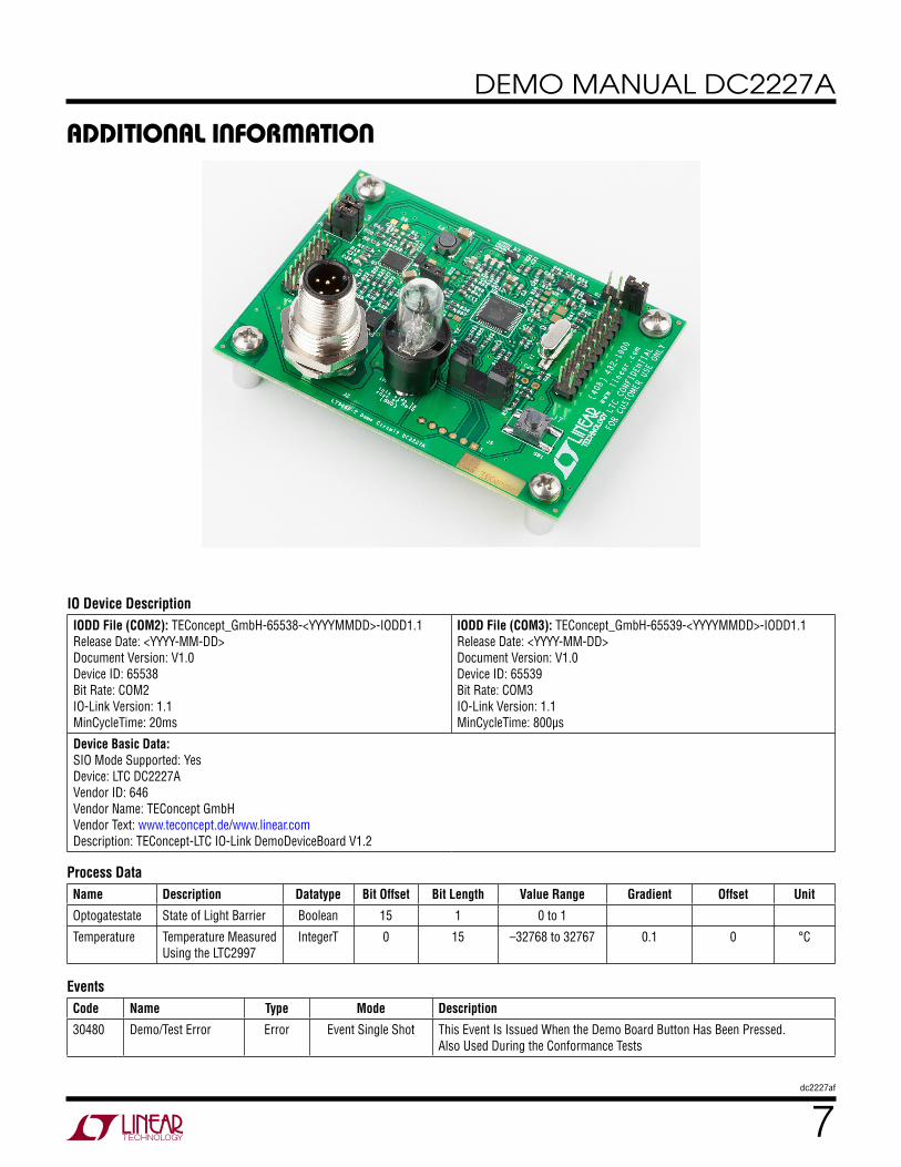
BoarD photo
A 28V/100mA light bulb connected to LT3669-2’s second driver (Q2) demonstrates its high current driving capabili-ties. All low voltage circuitry is supplied by the LT3669-2’s integrated buck and LDO for high efficiency.
Design files for this circuit board are available at http://www.linear.com/demo/DC2227A
Specifications are at TA = 25°C, VL+ = 24V
SYMBOL PARAMETER CONDITIONS MIN TYP MAX UNITS
L+ Input Supply 18 36 V
VBUCK LT3669-2's Buck Output Voltage 3.8 4 4.2 V
VLDO LT3669-2's LDO Output Voltage 3.135 3.3 3.465 V

2dc2227af
DEMO MANUAL DC2227A
Quick start proceDureAdditional Hardware and Software Requirements
To operate the DC2227A demo circuit in IO-Link mode, additional hardware and software are required:
• PC running Windows XP or later with Ethernet Card. Alternatively a USB-to-Ethernet adaptor can also be used
• LTC IO-Link Master Demo Circuit DC2228A
• DC2228A Control Tool Software
• PoE Injector or 24V Power Supply
• DC2227A IODD Files (COM2 and COM3)
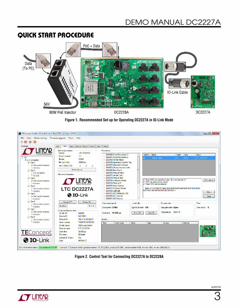
Set-up Preparation (See Figures 1 and 2)
1. Download and install the DC2228A Control Tool soft-ware from:
www.linear.com/demo/DC2228A
2. Connect the DC2228A to power and the host com-puter. Refer to the DC2228A demo manual for detailed information about the different configuration options to supply the DC2228A and interface it to the PC.
3. Using a 3-wire IO-Link cable of up to 20m in length with M12 connectors, plug the male terminal to one of the 8-ports of the DC2228A (for example port 2 like in Figure 1) and the female terminal to the DC2227A.
4. Run the DC2228A Control Tool on the PC and connect to the DC2228A. See the DC2228A demo manual for detailed information of how to select the DC2228A as the master, configure the IP parameters and establish communication between the host computer and the master.
Operation in IO-Link Mode (See Figures 1 and 2)
5. Download the DC2227A IODD files from:
www.linear.com/demo/DC2227A
6. Click on the “Select Device” button and import the IODD files by selecting the downloaded xml files and then clicking on the “Import” button (one at a time).
Operation in COM2
7. Click on the “Select Device” button again, this time making sure the correct port is selected. Use the fol-lowing IODD file:
TEConcept_GmbH-65538-<YYYYMMDD>-IODD1.1.xml
8. If the device is off, switch it on, enabling the L+ sup-ply of the connected master’s port by pressing the “Power ON” button keeping the light barrier open during power-up. If the device was already powered on coming from COM3 mode, power cycle it keeping the light barrier open to restart the device in COM2 mode. See the Light Barrier section for more information.
9. Start IO-Link communication by pressing the “IO-Link” button. The “Min. Cycle Time” is set to 20ms.
10. If a different IODD file is to be selected, stop IO-Link communication first by pressing the “Inactive” button to revert the DC2227A into SIO mode.
Operation in COM3
11. Click on the “Select Device” button again making sure the correct port is selected. Use the following IODD file:
TEConcept_GmbH-65539-<YYYYMMDD>-IODD1.1.xml
12. If the device is off, switch it on, enabling the L+ sup-ply of the connected master’s port by pressing the “Power ON” button keeping the light barrier closed during power-up. If the device was already powered on coming from COM2 mode, power cycle it keeping the light barrier closed to restart the device in COM3 mode. See the Light Barrier section for more information.
13. Start IO-Link communication by pressing the “IO-Link” button. The “Min. Cycle time” is set to 800µs.
14. If a different IODD file is to be selected, stop IO-Link communication first by pressing the “Inactive” button to revert the DC2227A in SIO mode.
3dc2227af
DEMO MANUAL DC2227A
Quick start proceDure
Figure 1. Recommended Set-up for Operating DC2227A in IO-Link Mode
Figure 2. Control Tool for Connecting DC2227A to DC2228A

4dc2227af
DEMO MANUAL DC2227A
aDDitional informationOperation in SIO Mode
The device can also operate in SIO mode. In this mode, no IO-Link communication takes place either because the master connected to the device is in the “Inactive” mode and it only supplies power to the device, or because there is no master connected to the device in which case the device is powered by a 24V supply. In SIO mode, the DC2227A reacts to the status of the light barrier as follows:
• If the light barrier is open, then drivers CQ1 and Q2 actively pull low. Since the onboard light bulb is con-nected between Q2 and ground, it is therefore turned off.
• If the light barrier is closed (by placing a piece of paper in its gap), CQ1 and Q2 actively pull high and the light bulb attached to Q2 turns on.
Temperature Sensor Configurations
In IO-Link mode, the DC2227A reports cyclically to the master (and thus to the PC Control Tool) the temperature measured by the on-board LTC2997. In order to measure temperature the LTC2997 uses an NPN configured as a diode. The NPN can be either on-chip, on PCB (Q1) or remote. Refer to the Connectors and Jumpers section for detailed information on how to choose the NPN.
Microcontroller ADC’s Offset Correction
The 12-bit ADC of the Atmel microcontroller samples both, the precise 1.8V reference voltage (VREF) and the VPTAT outputs of the LTC2997 to report the temperature in Celsius to the IO-Link master. The temperature is then calculated using a ratiometric measurement. The µC’s ADC is specified to have offsets from –40 to 40 LSBs. The temperature equation is:
100•T(°C)= ADC7 –OFFSET
ADC4–OFFSET• 45000 – 27315
ADC7 is the ADC’s code for the VPTAT output and ADC4 the code for the precise 1.8V VREF. OFFSET is the ADC’s offset (in LSB) parameter that can be set using the control tool (default is 0 LSB). In order to improve the accuracy of the temperature reading, a calibrated thermometer can be used to measure the temperature close to the LTC2997 and then the ADC Offset parameter can be set to the value (after several tries) that minimizes the error between the temperature reported by the Control Tool and that given by the calibrated thermometer.
Event Generator
The DC2227A is also equipped with a pushbutton to simulate events generated by IO-Link devices to inform IO-Link masters of requests that require special attention.
Light barrier
The light barrier offers many ways to interact with the device. It starts the device in COM3 mode if it is closed during power-up or in COM2 mode if left open. In IO-Link mode, its status is reported live on the PC control tool and in SIO mode its status is directly coupled to the CQ1 and Q2 drivers, thus allowing the user to operate the light bulb.
Light bulb
A 28V/100mA light bulb connects between Q2 and ground and serves to show the high current driving capability of the line drivers. It takes about 240ms to be turned on fully by the pulsing mechanism of the LT3669-2. To prevent data loss in IO-Link mode, driver Q2 is only enabled in between IO-Link telegrams. To turn it on and off from the control tool (in COM2 only) simply press the “Turn On” and “Turn Off” buttons within the light bulb section. In SIO mode, regardless on the IODD file chosen, the light bulb can be switched on and off by interacting with the light barrier.
5dc2227af
DEMO MANUAL DC2227A
aDDitional informationConnectors and Jumpers
The board has the following connectors:
Table 1. Connectors and Jumpers Overview
Name Type Form Comment
J1 Jumper Pin-2 Atmel µC Flash Erase
J2 Connector M12 IO-Link Signals (L+, L–, CQ1, Q2)
J3 Jumper Pin-2 LT3669-2 EN/UVLO Pin
J4 Header 8 × 2_2mm Eval Board DC1733
J5 Connector Pin-6 SPI Interface
J6 Jumper Pin-4 Sensor Selection
J7 JTAG Header10 × 2 JTAG Programming
J8 Jumper Pin-3 VDD3 Select
J9 Jumper Pin-3 Reset Select
Jumper J1
Jumper J1 sets the Erase/PB12 pin of the microcontroller to VDD3 (3.3V). By default the J1 header is not populated. For details about the Erase/PB12 pin see the ATSAM31S2AA microcontroller data sheet.
Connector J2
Connector J2 is a 5-pin M12 male connector. Plug a standard industrial sensor cable to this connector to sup-ply and communicate to the DC2227A using an IO-Link master. Table 2 shows the internal pin assignments to the LT3669-2 IO-Link PHY:
Table 2. Connector J2 Pinout
M12 Pin LT3669-2’s Pin Comment
1 L+ DC2227A Input Supply (24V)
2 Q2 LT3669-2 Second Driver
3 GND DC2227A Ground Node
4 CQ1 LT3669-2 Transceiver (IO-Link)
5 Not Connected
Jumper J3
Jumper J3 enables/disables the on board LT3669-2 (which also generates the internal 3.3V supply rail). Close this jumper (default position) to use the onboard LT3669-2 as the IO-Link PHY (it will start up for L+ voltages above 14.8V). Leave this jumper open if the external DC1733A-B board is used (via the J4 connector) as the IO-Link PHY instead.
Connector J4
J4 is for connecting an external DC1733A-B demo circuit bypassing the on-board LT3669-2. This connection allows access to more signals from LT3669-2. Connect jumper J3 from DC1733A-B pin-to-pin to jumper J4 on this board. Table 3 identifies each pin.
Table 3. Connector J4 PinoutPin Function Comment
1 TXD2 DC1733A-B Driver Input (Q2)
2 TXEN2 DC1733A-B Driver Input (Q2)
3 TXD1 DC1733A-B Driver Input (CQ1)
4 TXEN1 DC1733A-B Driver Input (CQ1)
5 RXD1 DC1733A-B Receiver Output (CQ1)
6 GND DC1733A-B Ground
7 WAKEn DC1733A-B Wake-Up Output
8 GND DC1733A-B Ground
9 SC2n DC1733A-B Driver Short Circuit Output (Q2)
10 SC1n DC1733A-B Driver Short Circuit Output (CQ1)
11 GND DC1733A-B Ground
12 RST_n DC1733A-B POR Reset Output
13 VDD(EXT) DC1733A-B LDO’s Output (3.3V)
14 GND DC1733A-B Ground
15 TP33 DC1733A-B Buck Output (5V)
16 SYNC DC1733A-B Buck Oscillator Synchronization Input
6dc2227af
DEMO MANUAL DC2227A
Connector J5
J5 is currently unused and may be helpful for the customer’s own applications that make use of the SPI interface of the Atmel microcontroller.
Table 4. Connector J5 SPI Pinout
Pin Function Comment
1 MISO Master In Slave Out
2 MOSI Master Out Slave In
3 SPCK SPI Clock
4 RESETn Reset
5 VDD3 Power
6 GND Ground
Jumper J6
J6 configures the sense device used by the LTC2997 to measure temperature. It could be either the LTC2997’s internal diode, the on-board diode-connected NPN Q1 or a remote NPN (connected as a diode) using a twisted pair:
Table 5. Jumper J6 Pinout (Temperature Sense Device)
Pin Description Comment
1 LTC2997’s VCC Close 1-2 to Use the LTC2997’s Int. NPN
2 LTC2997’s D+ To Base/Collector of Remote NPN
3 Q1’s Base/Collector Close 2-3 to Use the On-board NPN Q1
4 LTC2997’s D– To Emitter of Remote NPN
Connector J7
Standard 20-pin JTAG programming/debugging interface. This interface fits many JTAG/ICE connectors.
Table 6. JTAG Connector PinoutPin Function Comment
1, 2 VDD3
3 VDD3 Via 100k
5 TDI
7 TMS
9, 11 TCK
13 TDO
15 RESETn
17, 19 N.C.
6, 8, 10, 12, 14, 16, 18, 20 GND
aDDitional informationJumper J8
J8 selects the source for the VDD3 power.
Table 7. VDD3 Source Select Pinout
Pin Description Comment
1 DC1733A-B’s LDO Close 1-2 to Use DC1733A-B as PHY
2 Local VDD3 rail Default: Connected to Pin 3
3 Local LT3669-2’s LDO Close 2-3 to Use Local LT3669-2 as PHY
Jumper J9
J9 selects the source for the microcontroller’s reset pin.
Table 8. Reset Source Select Pinout
Pin Description Comment
1 DC1733A-B RSTn Close 1-2 to use DC1733A-B as PHY
2 Local RESETn Default: Connected to Pin 3
3 Local LT3669-2 RSTn Close 2-3 to Use Local LT3669-2 as PHY
Indicators
The following indicators are available:
Table 9. IndicatorsName Comment
LED1 ON (Green) if Device Is Powered up
LED2 ON (Red) if µC Started Successfully
LED3 ON (Red) if Device Is in IO-Link Mode
LP1 28V/100mA Light Bulb Between Q2 and GND
TVS Protection
The CQ1, Q2 and L+ pins are protected by 39V TVS diodes. Do not connect to any voltage higher than 36V.
Data Storage
Data Storage is not currently supported by DC2227A. Do not use pushbutton "DS upload" in Control Tool Software.
IO-Link Firmware
The firmware contained in the Atmel microcontroller is intellectual property owned by TEConcept GmbH in Germany. Any attempt to copy, transfer, or reverse en-gineer the firmware is forbidden. The source code or an object library for the IO-Link stack can be licensed from TEConcept.
7dc2227af
DEMO MANUAL DC2227A
aDDitional information
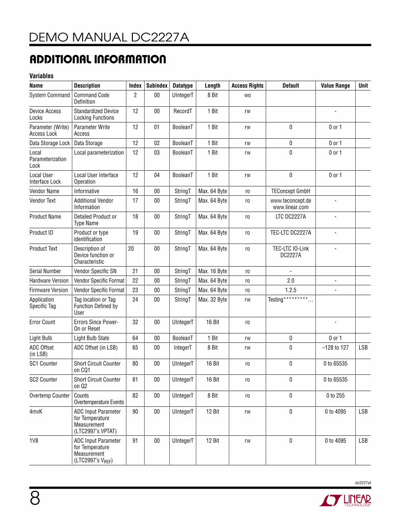
IO Device DescriptionIODD File (COM2): TEConcept_GmbH-65538-<YYYYMMDD>-IODD1.1Release Date: <YYYY-MM-DD>Document Version: V1.0Device ID: 65538Bit Rate: COM2IO-Link Version: 1.1MinCycleTime: 20ms
IODD File (COM3): TEConcept_GmbH-65539-<YYYYMMDD>-IODD1.1Release Date: <YYYY-MM-DD>Document Version: V1.0Device ID: 65539Bit Rate: COM3IO-Link Version: 1.1MinCycleTime: 800µs
Device Basic Data:SIO Mode Supported: YesDevice: LTC DC2227AVendor ID: 646Vendor Name: TEConcept GmbHVendor Text: www.teconcept.de/www.linear.com Description: TEConcept-LTC IO-Link DemoDeviceBoard V1.2
Process DataName Description Datatype Bit Offset Bit Length Value Range Gradient Offset Unit
Optogatestate State of Light Barrier Boolean 15 1 0 to 1
Temperature Temperature Measured Using the LTC2997
IntegerT 0 15 –32768 to 32767 0.1 0 °C
EventsCode Name Type Mode Description
30480 Demo/Test Error Error Event Single Shot This Event Is Issued When the Demo Board Button Has Been Pressed. Also Used During the Conformance Tests
8dc2227af
DEMO MANUAL DC2227A
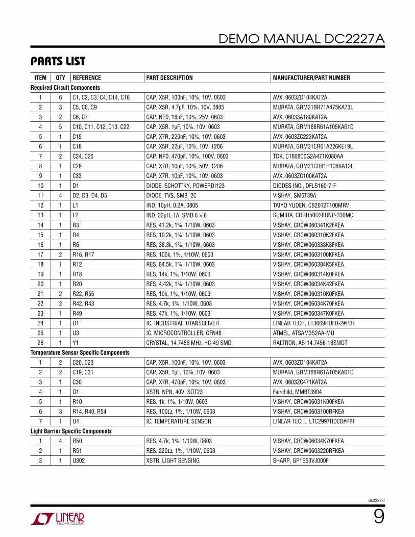
aDDitional informationVariablesName Description Index Subindex Datatype Length Access Rights Default Value Range Unit
System Command Command Code Definition
2 00 UIntegerT 8 Bit wo
Device Access Locks
Standardized Device Locking Functions
12 00 RecordT 1 Bit rw -
Parameter (Write) Access Lock
Parameter Write Access
12 01 BooleanT 1 Bit rw 0 0 or 1
Data Storage Lock Data Storage 12 02 BooleanT 1 Bit rw 0 0 or 1
Local Parameterization Lock
Local parameterization 12 03 BooleanT 1 Bit rw 0 0 or 1
Local User Interface Lock
Local User Interface Operation
12 04 BooleanT 1 Bit rw 0 0 or 1
Vendor Name Informative 16 00 StringT Max. 64 Byte ro TEConcept GmbH
Vendor Text Additional Vendor Information
17 00 StringT Max. 64 Byte ro www.teconcept.de www.linear.com
-
Product Name Detailed Product or Type Name
18 00 StringT Max. 64 Byte ro LTC DC2227A -
Product ID Product or type identification
19 00 StringT Max. 64 Byte ro TEC-LTC DC2227A -
Product Text Description of Device function or Characteristic
20 00 StringT Max. 64 Byte ro TEC-LTC IO-Link DC2227A
-
Serial Number Vendor Specific SN 21 00 StringT Max. 16 Byte ro -
Hardware Version Vendor Specific Format 22 00 StringT Max. 64 Byte ro 2.0 -
Firmware Version Vendor Specific Format 23 00 StringT Max. 64 Byte ro 1.2.5 -
Application Specific Tag
Tag location or Tag Function Defined by User
24 00 StringT Max. 32 Byte rw Testing*********…
Error Count Errors Since Power-On or Reset
32 00 UIntegerT 16 Bit ro -
Light Bulb Light Bulb State 64 00 BooleanT 1 Bit rw 0 0 or 1
ADC Offset (in LSB)
ADC Offset (in LSB) 65 00 IntegerT 8 Bit rw 0 –128 to 127 LSB
SC1 Counter Short Circuit Counter on CQ1
80 00 UIntegerT 16 Bit ro 0 0 to 65535
SC2 Counter Short Circuit Counter on Q2
81 00 UIntegerT 16 Bit ro 0 0 to 65535
Overtemp Counter Counts Overtemperature Events
82 00 UIntegerT 8 Bit ro 0 0 to 255
4mvK ADC Input Parameter for Temperature Measurement (LTC2997’s VPTAT)
90 00 UIntegerT 12 Bit rw 0 0 to 4095 LSB
1V8 ADC Input Parameter for Temperature Measurement (LTC2997’s VREF)
91 00 UIntegerT 12 Bit rw 0 0 to 4095 LSB
9dc2227af
DEMO MANUAL DC2227A
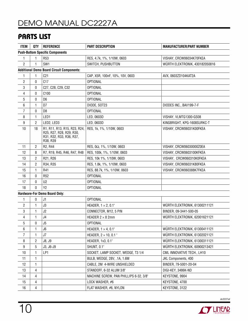
parts listITEM QTY REFERENCE PART DESCRIPTION MANUFACTURER/PART NUMBER
Required Circuit Components
1 6 C1, C2, C3, C4, C14, C16 CAP, X5R, 100nF, 10%, 10V, 0603 AVX, 0603ZD104KAT2A
2 3 C5, C8, C9 CAP, X5R, 4.7µF, 10%, 10V, 0805 MURATA, GRM21BR71A475KA73L
3 2 C6, C7 CAP, NP0, 18pF, 10%, 25V, 0603 AVX, 06033A180KAT2A
4 5 C10, C11, C12, C13, C22 CAP, X5R, 1µF, 10%, 10V, 0603 MURATA, GRM188R61A105KA61D
5 1 C15 CAP, X7R, 220nF, 10%, 10V, 0603 AVX, 0603ZC223KAT2A
6 1 C18 CAP, X5R, 22µF, 10%, 10V, 1206 MURATA, GRM31CR61A226KE19L
7 2 C24, C25 CAP, NP0, 470pF, 10%, 100V, 0603 TDK, C1608C0G2A471K080AA
8 1 C26 CAP, X7R, 10µF, 10%, 50V, 1206 MURATA, GRM31CR61H106KA12L
9 1 C33 CAP, X7R, 10pF, 10%, 10V, 0603 AVX, 0603ZC100KAT2A
10 1 D1 DIODE, SCHOTTKY, POWERDI123 DIODES INC., DFLS160-7-F
11 4 D2, D3, D4, D5 DIODE, TVS, SMB_2C VISHAY, SM6T39A
12 1 L1 IND, 10µH, 0.2A, 0805 TAIYO YUDEN, CB2012T100MRV
13 1 L2 IND, 33µH, 1A, SMD 6 × 6 SUMIDA, CDRH50D28RNP-330MC
14 1 R3 RES, 41.2k, 1%, 1/10W, 0603 VISHAY, CRCW060341K2FKEA
15 1 R4 RES, 10.2k, 1%, 1/10W, 0603 VISHAY, CRCW060310K2FKEA
16 1 R6 RES, 38.3k, 1%, 1/10W, 0603 VISHAY, CRCW060338K3FKEA
17 2 R16, R17 RES, 100k, 1%, 1/10W, 0603 VISHAY, CRCW0603100KFKEA
18 1 R12 RES, 84.5k, 1%, 1/10W, 0603 VISHAY, CRCW060384K5FKEA
19 1 R18 RES, 14k, 1%, 1/10W, 0603 VISHAY, CRCW060314K0FKEA
20 1 R20 RES, 4.42k, 1%, 1/10W, 0603 VISHAY, CRCW06034K42FKEA
21 2 R22, R55 RES, 10k, 1%, 1/10W, 0603 VISHAY, CRCW060310K0FKEA
22 2 R42, R43 RES, 4.7k, 1%, 1/10W, 0603 VISHAY, CRCW06034K70FKEA
23 1 R49 RES, 47k, 1%, 1/10W, 0603 VISHAY, CRCW060347K0FKEA
24 1 U1 IC, INDUSTRIAL TRANSCEIVER LINEAR TECH, LT3669HUFD-2#PBF
25 1 U3 IC, MICROCONTROLLER, QFN48 ATMEL, ATSAM3S2AA-MU
26 1 Y1 CRYSTAL, 14.7456 MHz, HC-49 SMD RALTRON, AS-14.7456-18SMDT
Temperature Sensor Specific Components
1 2 C20, C23 CAP, X5R, 100nF, 10%, 10V, 0603 AVX, 0603ZD104KAT2A
2 2 C19, C31 CAP, X5R, 1µF, 10%, 10V, 0603 MURATA, GRM188R61A105KA61D
3 1 C30 CAP, X7R, 470pF, 10%, 10V, 0603 AVX, 0603ZC471KAT2A
4 1 Q1 XSTR, NPN, 40V, SOT23 Fairchild, MMBT3904
5 1 R10 RES, 1k, 1%, 1/10W, 0603 VISHAY, CRCW06031K00FKEA
6 3 R14, R40, R54 RES, 100Ω, 1%, 1/10W, 0603 VISHAY, CRCW0603100RFKEA
7 1 U4 IC, TEMPERATURE SENSOR LINEAR TECH., LTC2997HDCB#PBF
Light Barrier Specific Components
1 4 R50 RES, 4.7k, 1%, 1/10W, 0603 VISHAY, CRCW06034K70FKEA
2 1 R51 RES, 220Ω, 1%, 1/10W, 0603 VISHAY, CRCW0603220RFKEA
3 1 U302 XSTR, LIGHT SENSING SHARP, GP1S53VJ000F
10dc2227af
DEMO MANUAL DC2227A
parts listITEM QTY REFERENCE PART DESCRIPTION MANUFACTURER/PART NUMBER
Push-Buttom Specific Components
1 1 R53 RES, 4.7k, 1%, 1/10W, 0603 VISHAY, CRCW06034K70FKEA
2 1 SW1 SWITCH, PUSHBUTTON WÜRTH ELEKTRONIK, 430182050816
Additional Demo Board Circuit Components:
1 1 C21 CAP, X5R, 100nF, 10%, 10V, 0603 AVX, 0603ZD104KAT2A
2 0 C17 OPTIONAL
3 0 C27, C28, C29, C32 OPTIONAL
4 0 C100 OPTIONAL
5 0 D6 OPTIONAL
6 1 D7 DIODE, SOT23 DIODES INC., BAV199-7-F
7 0 D8 OPTIONAL
8 1 LED1 LED, 0603D VISHAY, VLMTG1300-GS08
9 2 LED2, LED3 LED, 0603D KINGBRIGHT, KPG-1608SURKC-T
10 18 R1, R11, R13, R15, R23, R24, R25, R27, R28, R29, R30, R31, R32, R33, R36, R37, R38, R39
RES, 1k, 1%, 1/10W, 0603 VISHAY, CRCW06031K00FKEA
11 2 R2, R44 RES, 0Ω, 1%, 1/10W, 0603 VISHAY, CRCW06030000Z0EA
12 8 R7, R19, R45, R46, R47, R48 RES, 100k, 1%, 1/10W, 0603 VISHAY, CRCW0603100KFKEA
13 2 R21, R26 RES, 10k 1%, 1/10W, 0603 VISHAY, CRCW060310K0FKEA
14 2 R34, R35 RES, 1.8k, 1%, 1/10W, 0603 VISHAY, CRCW06031K80FKEA
15 1 R41 RES, 88.7k, 1%, 1/10W, 0603 VISHAY, CRCW060388K7FKEA
16 0 R52 OPTIONAL
17 0 U2 OPTIONAL
18 0 Y2 OPTIONAL
Hardware-For Demo Board Only:
1 0 J1 OPTIONAL
2 1 J3 HEADER, 1 × 2, 0.1" WÜRTH ELEKTRONIK, 61300211121
3 1 J2 CONNECTOR, M12, 5 PIN BINDER, 09-3441-500-05
4 1 J4 HEADER 2 × 8 2mm WÜRTH ELEKTRONIK, 62001621121
5 0 J5 OPTIONAL
6 1 J6 HEADER, 1 × 4, 0.1" WÜRTH ELEKTRONIK, 61300411121
7 1 J7 HEADER, 2 × 10, 0.1 " WÜRTH ELEKTRONIK, 61302021121
8 2 J8, J9 HEADER, 1x3, 0.1" WÜRTH ELEKTRONIK, 61300311121
9 5 J3, J6-J9 SHUNT, 0.1" WÜRTH ELEKTRONIK, 60900213421
10 1 LP1 SOCKET, LAMP SOCKET, WEDGE, T3 1/4 CML INNOVATIVE TECH., LH10
11 1 BULB, WEDGE, 28V, .1A, 1.6M JKL Components, 400
12 1 CABLE, 2M 4-WIRE UNSHIELDED BINDER, 79-5001-20-04
13 4 STANDOFF, 6-32 ALUM 3/8" DIGI-KEY, 3486K-ND
14 4 MACHINE SCREW, PAN PHILLIPS 6-32, 3/8" KEYSTONE, 9904
15 4 LOCK WASHER, #6 KEYSTONE, 4700
16 4 FLAT WASHER, #6, NYLON KEYSTONE, 3122

11dc2227af
DEMO MANUAL DC2227A
Information furnished by Linear Technology Corporation is believed to be accurate and reliable. However, no responsibility is assumed for its use. Linear Technology Corporation makes no representa-tion that the interconnection of its circuits as described herein will not infringe on existing patent rights.
schematic Diagram5 5
4 4
3 3
2 2
1 1
DD
CC
BB
AA
LED green
SMD or THT
TEMP-Sensor
to demoboard DC1733
optional
enable internal Pullup: PA0, PA1, PA3
SDA
SCL
LED red
Orbitec_OR1206_BA9
TE CONNECTIVITY / ALCOSWITCH
5V not needed
3.28V
J6:
Jumper 1-2 internal LTC2997 Sensor selected
Jumper 2-3 Sensor Q1 selected
ext. Diode wired to Pin 2 and Pin 4, no Jumper
1630 McCarthy Blvd.
Milpitas, CA 95035
Phone: (408) 432-1900
Fax: (408) 434-0507
www.linear.com
LTC CONFIDENTIAL FOR CUSTOMER USE ONLY
CUSTOMER NOTICE
LINEAR TECHNOLOGY HAS MADE A BEST EFFORT
TO DESIGN A CIRCUIT THAT MEETS CUSTOMER -
SUPPLIED SPECIFICATIONS; HOWEVER, IT REMAINS
THE CUSTOMERS RESPONSIBILITY TO VERIFY
PROPER AND RELIABLE OPERATION IN THE ACTUAL
APPLICATION. COMPONENT SUBSTITUTION AND
PRINTED CIRCUIT LAYOUT MAY SIGNIFICANTLY
AFFECT CIRCUIT PERFORMANCE OR RELIABILITY.
CONTACT LINEAR TECHNOLOGY APPLICATIONS
ENGINEERING FOR ASSISTANCE.
THIS CIRCUIT IS PROPRIETARY TO
LINEAR TECHNOLOGY AND SUPPLIED FOR
USE WITH LINEAR TECHNOLOGY PARTS.
TEConcept GmbH Wentzingerstr. 21 D 79106 Freiburg
tel.: +49-761 214436-0 www.teconcept.de
ground terminal should
be the external case of
light bulb socket!
50V
BST
SW
SYN
C
FBld
o
FBou
t
CPO
R
RT
SC1n
WAK
En
DA
WAK
En
TXD
2TX
D1
RXD
1
TXEN
2TX
EN1
SC2n
SC1n
SC2n
SYN
C
SR
TXEN
1
TXD
1
TXEN
2
TXD
2
Q2
CQ
1
DIO
SC2n
SR
TXD
2
RES
ETn
TXD1
Vpll
TDO
TMS
TCK
LED
MISO
MOSI
SPCK
Opt
o
SWIT
CH
D+
D-
TDI
SC1n
TDI
TMS
TCK
TDO
RES
ETn
Q2
EN
L+
RXD
1
TXEN
2
TXEN
1
RXD
2W
AKEn
RES
ETn
Opt
o
LED
SWIT
CH
RST
_nR
ESET
n
RST
_n
LDO
in
EN
L+D
IO
L+
RXD1
RST
n
CPO
R
0
0
0
00
00
0
0
0
VDD
3x
0
0
VDD
3
0
0 0
1V8r
ef
0
VDD
18
00
VDD
3
VDD
18
VDD
18
VDD
3
VDD
18
0
VDD
3
00
0
VDD
3
0
0
VDD
3
VDD
3VD
D3
VDD
18
00
0
00
00
0
0
VDD
3
0
1V8r
ef
0
0
0
0
00
0
00
00
VDD
3
VDD
30
0
VDD
3
0
VDD
3
0
VDD
3x
VDD
3
VDD
3
VDD
3
0
0
0
VDD
3
0
VDD
3
0
RST
n
4mV/
K
4mV/
K
RST
n
Title
Size
Rev
Dat
e:Sh
eet
of
1.1
LT36
69 D
EMO
CIR
CU
IT D
C22
27A
A3
18
Wed
nesd
ay, N
ovem
ber 0
5, 2
014
Title
Size
Rev
Dat
e:Sh
eet
of
1.1
LT36
69 D
EMO
CIR
CU
IT D
C22
27A
A3
18
Wed
nesd
ay, N
ovem
ber 0
5, 2
014
Title
Size
Rev
Dat
e:Sh
eet
of
1.1
LT36
69 D
EMO
CIR
CU
IT D
C22
27A
A3
18
Wed
nesd
ay, N
ovem
ber 0
5, 2
014
TP8
TP81
R41
88.7
kR
4188
.7k
C11
1uF
C11
1uF
R371k R371k
R51
220RR
5122
0R
C29
DN
PC
29D
NP
R2
0RR2
0R
C17
DN
PC
17D
NP
U4
LTC
2997
HD
CB
U4
LTC
2997
HD
CB
D+
1
D-
2VP
TAT
3
VCC4 GND 5
Vref
6
PP 7
C10
1uF
C10
1uF
C15
220n
F_X7
RC
1522
0nF_
X7R
L1 10uH
L1 10uH
12
D1
DFL
S160
D1
DFL
S160
R16
100k
R16
100k
TP3
TP3 1
Q1
MM
BT39
04
Q1
MM
BT39
04
1
23
TP29
Hol
e4m
mTP
29H
ole4
mm
1
R30
1kR
301k
D4
SM6T
39A
D4
SM6T
39A
C4
100n
FC
410
0nF
TP19 TP191
TP14
TP14
1
R14
100R
R14
100R
J1 DN
PJ1 D
NP
1 2
R40
100R
R40
100R
R361k R361k
D3
SM6T
39A
D3
SM6T
39A
R34
1.8k
R34
1.8k
Y2 DN
P
Y2 DN
P
R27
1kR
271k
C3
100n
FC
310
0nF
TP10
TP10
1
C2
100n
FC
210
0nF
R1
1kR1
1k
C18
22uF
_X5R
C18
22uF
_X5R
J7 JTAG
J7 JTAG
12
34
56
78
910
1112
1314
1516
1718
1920
J9Ju
mpe
r2-3
J9Ju
mpe
r2-3
123
R3
41.2
kR
341
.2k
R45
100k
R45
100k
LED
2
KPG
-160
8SU
RKC
-T
LED
2
KPG
-160
8SU
RKC
-T
C23
100n
FC
2310
0nF
R28
1kR
281k
D6
DN
PD
6D
NP
TP28
Hol
e4m
mTP
28H
ole4
mm
1
R12
84.5
kR
1284
.5k
R55
10k
R55
10k
L2 CD
RH
50D
28R
NP-
330M
CL2 C
DR
H50
D28
RN
P-33
0MC
12
LED
1VL
MTG
1300
-GS0
8LE
D1
VLM
TG13
00-G
S08
R54
100R
R54
100R
TP24
Fidu
cial
TP24
Fidu
cial
1
C7
18pF
C7
18pF
C9
4.7u
FC
94.
7uF
R11
1kR
111k
C1
100n
FC
110
0nF
TP22
TP221
TP21
TP21
1
R32
1kR
321k
R22
10k
R22
10k
U2
DN
PU2
DN
PIN1
OU
T2
GND 3
R53
4.7k
R53
4.7k
R15
1kR15
1k
U3
ATSA
M3S
2AA-
MU
U3
ATSA
M3S
2AA-
MU
ADVR
EF1
GN
D2
2
PB0/
AD4
3
PB1/
AD5
4
PB2/
AD6
5
PB3/
AD7
6
VDD
IN7
VDD
OU
T8
PA17
/PG
MD
5/AD
09
PA18
/PG
MD
6/AD
110
PA19
/PG
MD
7/AD
211
PA20
/AD
312
VDDIO13 13
PA16/PGMD4 14
PA15/PGMD3 15
PA14/PGMD2 16
PA13/PGMD1 17
VDDCORE 18
PA12/PGMD0 19
PA11/PGMM3 20
PA10/PGMM2 21
PA9/PGMM1 22
PA8/XOUT32/PGMM0 23
PA7/XIN32/PGMNVALID 24
TDI/P
B425
PA6/
PGM
NO
E26
PA5/
PGM
RD
Y27
PA4/
PGM
NC
MD
28
NR
ST29
TST
30
PA3
31
PA2/
PGM
EN2
32
VDD
IO33
33
GN
D34
34
PA1/
PGM
EN1
35
PA0/
PGM
EN0
36
TDO/TRACESWO/PB537
JTAGSEL38
TMS/SWDIO/PB639
TCK/SWCLK/PB740
VDDCORE4141
ERASE/PB1242
DDM/PB1043
DDP/PB1144
XOUT/PB845
XIN/PB9/PGMCK46
VDDIO4747
VDDPLL48
PP49
TP20
TP20
1
C6
18pF
C6
18pF
R35
1.8k
R35
1.8k
R46
100k
R46
100k
J6
Jum
per
J6
Jum
per1 2 3 4
C5
4.7u
FC
54.
7uF
TP25
Fidu
cial
TP25
Fidu
cial
1
R31
1kR
311k
R10
1kR
101k
C13
1uF
C13
1uF
C28
DN
PC
28D
NP
Y1
14.7
456M
Hz
Y1
14.7
456M
Hz
12
LED
3
KPG
-160
8SU
RKC
-T
LED
3
KPG
-160
8SU
RKC
-T
J2
Bind
er_0
9-34
41-5
00-0
5
J2
Bind
er_0
9-34
41-5
00-0
5
1 2 3 4 567
TP33
TP331
LP1
28V1
00m
A
LP1
28V1
00m
A
12
TP6
TP6
1
TP1
TP1 1
TP31
Hol
e4m
mTP
31H
ole4
mm
1
TP15
TP15
1
D7
BAV1
99D
7BA
V199
21
3
TP35
Fidu
cial
TP35
Fidu
cial
1
R13
1kR
131k
R33
1kR
331k
C19
1uF
C19
1uF
TP17
TP17
1
TP18
TP18
1
R25
1kR
251k
R6
38.3
kR
638
.3k
R38
1kR
381k
U30
2G
P1S5
3VJ0
00F
U30
2G
P1S5
3VJ0
00F
1 2
3 4
R49
47k
R49
47k
R42
4.7k
R42
4.7k
J4
HEA
DER
2X8
2M
M
J4
HEA
DER
2X8
2M
M
12
34
56
78
910
1112
1314
1516
R47
100k
R47
100k
TP9
TP9
1
TP26
Fidu
cial
TP26
Fidu
cial
1
R19
100k
R19
100k
R7
100k
R7
100k
R50
4.7k
R50
4.7k
SW1
FSM
4JSM
A
SW1
FSM
4JSM
A
1 234
U1
LT36
69H
UFD
-2
U1
LT36
69H
UFD
-2
BD17
LDO
in18
SW15
BST
16
SYN
C24
SR25
RST
n28
SC1n
1
SC2n
2
WAK
En3
RXD
14
TXEN
15
TXD
16
TXEN
27
TXD
28
GND29 29D
A14
CQ
110
Q2
9
L+11
EN/U
VLO
12
DIO
13
AGN
D23
FBLD
O20
LDO
19
ILIM
26
RT
22
CPO
R27
FBou
t21
TP27
Fidu
cial
TP27
Fidu
cial
1
C31
1uF
C31
1uF
J5 DN
PJ5 D
NP
1 2 3 4 5 6
J3 Jum
per
J3 Jum
per
12
R24
1kR
241k
R52
DN
PR
52D
NP
TP30
Hol
e4m
mTP
30H
ole4
mm
1
TP34
Fidu
cial
TP34
Fidu
cial
1
PT21PTPT21PT
1
C25
470p
F_10
0VC
2547
0pF_
100V
TP23
TP231
C14
100n
FC
1410
0nF
D2
SM6T
39A
D2
SM6T
39A
C16
100n
FC
1610
0nF
R4
10.2
kR
410
.2k
J8Ju
mpe
r2-3
J8Ju
mpe
r2-3
123
R48
100k
R48
100k
C10
0O
ptio
nal_
Tant
al_A
C10
0O
ptio
nal_
Tant
al_A
R18
14k
R18
14k
TP5
TP5
1
R29
1kR
291k
C26
10uF
_50V
_X7R
C26
10uF
_50V
_X7R
R44
0RR44
0R
R39
1kR
391k
R17
100k
R17
100k
D5
SM6T
39A
D5
SM6T
39A
C8
4.7u
F_X5
RC
84.
7uF_
X5R
TP32
TP32 1
C20
100n
FC
2010
0nF
R21
10k
R21
10k
PT4PTPT4PT
1
C27
DN
PC
27D
NP
TP13
TP13
1
R26
10k
R26
10k
C30
470p
C30
470p
C24
470p
F_10
0VC
2447
0pF_
100V
TP11
TP11
1R
204.
42k
R20
4.42
k
R43
4.7k
R43
4.7k
R23
1kR
231k
C21
100n
FC
2110
0nF
C12
1uF
C12
1uF
C22
1uF
C22
1uF
D8
DN
P
D8
DN
P
TP16
TP16
1
C32
DN
PC
32D
NP
TP2
TP2 1
C33
10pF
C33
10pF

12dc2227af
DEMO MANUAL DC2227A
Linear Technology Corporation1630 McCarthy Blvd., Milpitas, CA 95035-7417 (408) 432-1900 ● FAX: (408) 434-0507 ● www.linear.com LINEAR TECHNOLOGY CORPORATION 2015
LT 0415 • PRINTED IN USA
DEMONSTRATION BOARD IMPORTANT NOTICE
Linear Technology Corporation (LTC) provides the enclosed product(s) under the following AS IS conditions:
This demonstration board (DEMO BOARD) kit being sold or provided by Linear Technology is intended for use for ENGINEERING DEVELOPMENT OR EVALUATION PURPOSES ONLY and is not provided by LTC for commercial use. As such, the DEMO BOARD herein may not be complete in terms of required design-, marketing-, and/or manufacturing-related protective considerations, including but not limited to product safety measures typically found in finished commercial goods. As a prototype, this product does not fall within the scope of the European Union directive on electromagnetic compatibility and therefore may or may not meet the technical requirements of the directive, or other regulations.
If this evaluation kit does not meet the specifications recited in the DEMO BOARD manual the kit may be returned within 30 days from the date of delivery for a full refund. THE FOREGOING WARRANTY IS THE EXCLUSIVE WARRANTY MADE BY THE SELLER TO BUYER AND IS IN LIEU OF ALL OTHER WARRANTIES, EXPRESSED, IMPLIED, OR STATUTORY, INCLUDING ANY WARRANTY OF MERCHANTABILITY OR FITNESS FOR ANY PARTICULAR PURPOSE. EXCEPT TO THE EXTENT OF THIS INDEMNITY, NEITHER PARTY SHALL BE LIABLE TO THE OTHER FOR ANY INDIRECT, SPECIAL, INCIDENTAL, OR CONSEQUENTIAL DAMAGES.
The user assumes all responsibility and liability for proper and safe handling of the goods. Further, the user releases LTC from all claims arising from the handling or use of the goods. Due to the open construction of the product, it is the user’s responsibility to take any and all appropriate precautions with regard to electrostatic discharge. Also be aware that the products herein may not be regulatory compliant or agency certified (FCC, UL, CE, etc.).
No License is granted under any patent right or other intellectual property whatsoever. LTC assumes no liability for applications assistance, customer product design, software performance, or infringement of patents or any other intellectual property rights of any kind.
LTC currently services a variety of customers for products around the world, and therefore this transaction is not exclusive.
Please read the DEMO BOARD manual prior to handling the product. Persons handling this product must have electronics training and observe good laboratory practice standards. Common sense is encouraged.
This notice contains important safety information about temperatures and voltages. For further safety concerns, please contact a LTC applica-tion engineer.
Mailing Address:
Linear Technology
1630 McCarthy Blvd.
Milpitas, CA 95035
Copyright © 2004, Linear Technology Corporation