datasheet - distec.de · liquid crystal display (a-si tft lcd) panel structure with driver lsis for...
TRANSCRIPT

The information contained in this document has been carefully researched and is, to the best of our knowledge, accurate. However, we assume no liability for any product failures or damages, immediate or consequential, resulting from the use of the information provided herein. Our products are not intended for use in systems in which failures of product could result in personal injury. All trademarks mentioned herein are property of their respective owners. All specifications are subject to change without notice.
Datasheet Tianma
NL192108AC18-02D 15.6" TFT Display
NL-01-006
Document Number: DOD-PP-3095 (2nd edition) Published date: April 2019 CP(N)
Tianma Japan, Ltd. 2017-2019 All rights reserved.
1
This DATA SHEET is updated document from DATA SHEET DOD-PP-2571(1) All information is subject to change without notice. Please confirm the sales representative before starting to design your system.
TFT COLOR LCD MODULE
NL192108AC18-02D
40cm (15.6 Type) FHD
LVDS interface (2 ports)
DATA SHEET DOD-PP-3095 (2nd edition)
NL192108AC18-02D
DATA SHEET DOD-PP-3095 (2nd edition) 2 2 2
INTRODUCTION
The Copyright to this document belongs to Tianma Japan, Ltd. (hereinafter called "TMJ"). No part of this
document will be used, reproduced or copied without prior written consent of TMJ.
TMJ does and will not assume any liability for infringement of patents, copyrights or other intellectual property rights of any third party arising out of or in connection with application of the products described herein except for that directly attributable to mechanisms and workmanship thereof. No license, express or implied, is granted under any patent, copyright or other intellectual property right of TMJ.
Some electronic products would fail or malfunction at a certain rate. In spite of every effort to enhance
reliability of products by TMJ, the possibility of failures and malfunction might not be avoided entirely. To prevent the risks of damage to death, human bodily injury or other property arising out thereof or in connection therewith, each customer is required to take sufficient measures in its safety designs and plans including, but not limited to, redundant system, fire-containment and anti-failure.
The products are classified into three grades: "Standard", "Special", and "Specific". Each quality grade is designed for applications described below. Any customer who intends to use a
product for application other than that of Standard is required to contact TMJ sales representative in advance.
The Standard: Applications as any failure, malfunction or error of the products are free from any damage to death, human bodily injury or other property (Products Safety Issue) and not related the safety of the public (Social Issues), like general electric devices. Examples: Office equipment, audio and visual equipment, communication equipment, test and
measurement equipment, personal electronic equipment, home electronic appliances, car navigation system (with no vehicle control functions), seat entertainment monitor for vehicles and airplanes, fish finder (except marine radar integrated type), PDA, etc.
The Special: Applications as any failure, malfunction or error of the products might directly cause any damage to death, human bodily injury or other property (Products Safety Issue) and the safety of the public (Social Issues) and required high level reliability by conventional wisdom. Examples: Vehicle/train/ship control system, traffic signals system, traffic information control system, air
traffic control system, surgery/operation equipment monitor, disaster/crime prevention system, etc.
The Specific: Applications as any failure, malfunction or error of the products might severe cause any damage to death, human bodily injury or other property (Products Safety Issue) and the safety of the public (Social Issues) and developed, designed and manufactured in accordance with the standards or quality assurance program designated by the customer who requires extremely high level reliability and quality. Examples: Aerospace system (except seat entertainment monitor), nuclear control system, life support
system, etc.
The quality grade of this product is the "Standard" unless otherwise specified in this document.
NL192108AC18-02D
DATA SHEET DOD-PP-3095 (2nd edition) 3 3 3
CONTENTS
INTRODUCTION ........................................................................................................................................ 2
1. OUTLINE .................................................................................................................................................. 4
1.1 STRUCTURE AND PRINCIPLE ........................................................................................................ 4 1.2 APPLICATION .................................................................................................................................... 4 1.3 FEATURES .......................................................................................................................................... 4
2. GENERAL SPECIFICATIONS .............................................................................................................. 5 3. BLOCK DIAGRAM ................................................................................................................................. 6 4. DETAILED SPECIFICATIONS ............................................................................................................. 7
4.1 MECHANICAL SPECIFICATIONS ................................................................................................... 7 4.2 ABSOLUTE MAXIMUM RATINGS .................................................................................................. 7 4.3 ELECTRICAL CHARACTERISTICS ................................................................................................. 8
4.3.1 LCD panel signal processing board ............................................................................................. 8 4.3.2 LED driver ................................................................................................................................... 9 4.3.3 Fuse .............................................................................................................................................. 9
4.4 POWER SUPPLY VOLTAGE SEQUENCE ..................................................................................... 10 4.4.1 LCD panel signal processing board ........................................................................................... 10 4.4.2 LED driver ................................................................................................................................. 11
4.5 CONNECTIONS AND FUNCTIONS FOR INTERFACE PINS ...................................................... 12 4.5.1 LCD panel signal processing board ........................................................................................... 12 4.5.2 LED driver ................................................................................................................................. 13 4.5.3 Positions of socket ..................................................................................................................... 13 4.5.4 Input data mapping .................................................................................................................... 14
4.6 DISPLAY COLORS AND INPUT DATA SIGNALS ....................................................................... 15 4.7 DISPLAY POSITIONS ...................................................................................................................... 16 4.8 INPUT SIGNAL TIMINGS ............................................................................................................... 17
4.8.1 Outline of input signal timings .................................................................................................. 17 4.8.2 Timing characteristics ................................................................................................................ 18 4.8.3 Input signal timing chart ............................................................................................................ 19
4.9 LVDS Rx AC SPEC ........................................................................................................................... 20 4.10 OPTICS ............................................................................................................................................. 21
4.10.1 Optical characteristics .............................................................................................................. 21 4.10.2 Definition of contrast ratio ....................................................................................................... 22 4.10.3 Definition of luminance uniformity ......................................................................................... 22 4.10.4 Definition of response times .................................................................................................... 22 4.10.5 Definition of viewing angles .................................................................................................... 22
5. ESTIMATED LUMINANCE LIFETIME ............................................................................................ 23 6. RELIABILITY TESTS .......................................................................................................................... 24 7. PRECAUTIONS ..................................................................................................................................... 25
7.1 MEANING OF CAUTION SIGNS .................................................................................................... 25 7.2 CAUTIONS ........................................................................................................................................ 25 7.3 ATTENTIONS.................................................................................................................................... 25
7.3.1 Handling of the product ............................................................................................................. 25 7.3.2 Environment............................................................................................................................... 26 7.3.3 Characteristics ............................................................................................................................ 26 7.3.4 Others ......................................................................................................................................... 27
8. OUTLINE DRAWINGS ......................................................................................................................... 28 8.1 FRONT VIEW .................................................................................................................................... 28 8.2 REAR VIEW ...................................................................................................................................... 29
NL192108AC18-02D
DATA SHEET DOD-PP-3095 (2nd edition) 4 4 4
1. OUTLINE
1.1 STRUCTURE AND PRINCIPLE
Color LCD module NL192108AC18-02D is composed of the amorphous silicon thin film transistor liquid crystal display (a-Si TFT LCD) panel structure with driver LSIs for driving the TFT (Thin Film Transistor) array and a backlight.
The a-Si TFT LCD panel structure is injected liquid crystal material into a narrow gap between the TFT array glass substrate and a color-filter glass substrate.
Color (Red, Green, Blue) data signals from a host system (e.g. signal generator, etc.) are modulated into best form for active matrix system by a signal processing board, and sent to the driver LSIs which drive the individual TFT arrays.
The TFT array as an electro-optical switch regulates the amount of transmitted light from the backlight assembly, when it is controlled by data signals. Color images are created by regulating the amount of transmitted light through the TFT array of red, green and blue dots.
1.2 APPLICATION
• For industrial use
1.3 FEATURES
• Ultra-Wide viewing angle (Super Fine TFT (SFT)) • High resolution • High contrast • Wide color gamut • LVDS interface • 8-bit digital signals for data of RGB • Narrow border • LED backlight built in LED driver • Acquisition product for UL60950-1 /CSA C22.2 No.60950-1-03 (File number: E170632) • Compliant with the European RoHS directive (2011/65/EU)
NL192108AC18-02D
DATA SHEET DOD-PP-3095 (2nd edition) 5 5 5
2. GENERAL SPECIFICATIONS
Display area 344.16 (H) × 193.59 (V) mm Diagonal size of display 40cm (15.6 inches) Drive system a-Si TFT active matrix Display color 16,777,216 colors Pixel 1,920 (H) × 1,080 (V) pixels Pixel arrangement RGB (Red dot, Green dot, Blue dot) vertical stripe
Dot pitch 0.05975 (H) × 0.17925 (V) mm Pixel pitch 0.17925 (H) × 0.17925 (V) mm Module size 363.8 (W) × 215.9 (H) × 6.3 (D) mm (typ.) Weight 610g (typ.)
Contrast ratio 1,000:1 (typ.)
Viewing angle At the contrast ratio ≥10:1
• Horizontal: Right side 88° (typ.), Left side 88° (typ.) • Vertical: Up side 88° (typ.), Down side 88° (typ.)
Designed viewing direction Viewing angle with optimum grayscale (γ≒2.2): Normal axis (perpendicular)
Polarizer surface Antiglare Polarizer pencil-hardness 3H (min.) [by JIS K5600]
Color gamut At LCD panel center 72% (typ.) [against NTSC color space]
Response time Ton+Toff (10%←→ 90%) 25ms (typ.)
Luminance At the maximum luminance control 400cd/m2 (typ.)
Signal system LVDS interface (2 ports) [8-bit digital signals for data of RGB colors, Dot clock (CLK), Data enable (DE)]
Power supply voltage LCD panel signal processing board: 3.3V LED driver: 12.0V
Backlight LED backlight built in LED driver
Power consumption At the maximum luminance control, Checkered flag pattern 13.7W (typ.)
NL192108AC18-02D
DATA SHEET DOD-PP-3095 (2nd edition) 6 6 6
3. BLOCK DIAGRAM
Note1: Relation between GND (Signal ground and LED driver ground) and FG (Frame ground) in the LCD module is as follows. GND- FG Connected
Note2: GND and FG must be connected to customer equipment’s ground, and it is recommended that these grounds to be connected together in customer equipment.
Note3: Each pair of the LVDS signal has a 100Ω terminating resistance.
LVD
S pa
rt
LV
DS
part
Con
trolle
r with
rece
iver
for L
VD
S
Note1 Note2
LCD panel signal processing board
Host
5,760 lines
LCD panel H: 1,920 × 3 (R, G, B) V: 1,080
1,08
0 lin
es
VCC
LCD module (Product)
Fuse
H-driver
FG
DB0+ DB0-
Note1 Note2
V-d
river
Power supply for gradation
DB1+ DB1- DB2+ DB2- DB3+ DB3- CLKB+ CLKB-
DC/DC converter
LED Backlight
VDD Fuse
GND
PWM
BRTC
DA0+ DA0- DA1+ DA1- DA2+ DA2- DA3+ DA3- CLKA+ CLKA-
GND
100k
Ω
LED driver
39kΩ
100k
Ω
39kΩ
Note3
NL192108AC18-02D
DATA SHEET DOD-PP-3095 (2nd edition) 7 7 7
4. DETAILED SPECIFICATIONS
4.1 MECHANICAL SPECIFICATIONS
Parameter Specification Unit
Module size 363.8 ± 0.5 (W) × 215.9 ± 0.5 (H) × 6.3 ± 0.5 (D) Note1 mm
Display area 344.16 (H) × 193.59 (V) Note1 mm
Weight 610 (typ.), 670 (max.)
g
Note1: See "8. OUTLINE DRAWINGS".
4.2 ABSOLUTE MAXIMUM RATINGS
Parameter Symbol Rating Unit Remarks
Power supply voltage
LCD panel signal processing board VCC -0.3 to +4.0 V
Ta = 25°C
LED driver VDD -0.3 to +15.0
Input voltage for signals
LCD panel signal processing board
Display signals Note1
VD -0.3 to VCC+0.3 V
LED driver PWM -0.3 to +5.5 V
BRTC -0.3 to +5.5 V
Storage temperature Tst -20 to +70 °C -
Operating temperature Front surface TopF -20 to +70 °C Note2
Rear surface TopR -20 to +70 °C Note3
Relative humidity Note4 RH
≤ 95 % Ta ≤ 40°C
≤ 85 % 40°C < Ta ≤ 50°C
≤ 55 % 50°C < Ta ≤ 60°C
≤ 36 % 60°C < Ta ≤ 70°C
Absolute humidity Note4 AH ≤ 70
Note5 g/m3 Ta = 70°C
Note1: DA0+/-, DA1+/-, DA2+/-, DA3+/- ,CLKA+/-, DB0+/-, DB1+/-, DB2+/-, DB3+/-, CLKB+/- Note2: Measured at LCD panel surface (including self-heat) Note3: Measured at LCD module's rear shield surface (including self-heat) Note4: No condensation Note5: Water amount at Ta= 70°C and RH= 36%
NL192108AC18-02D
DATA SHEET DOD-PP-3095 (2nd edition) 8 8 8
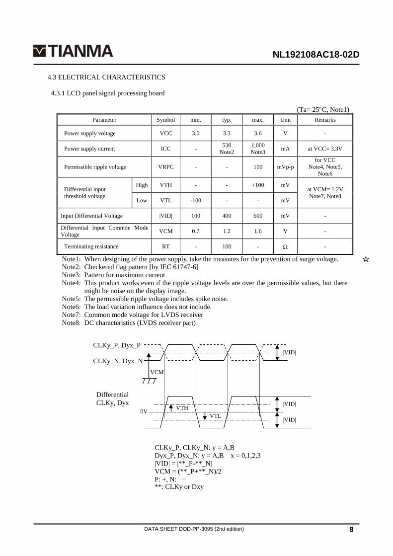
4.3 ELECTRICAL CHARACTERISTICS
4.3.1 LCD panel signal processing board
(Ta= 25°C, Note1)
Parameter Symbol min. typ. max. Unit Remarks
Power supply voltage VCC 3.0 3.3 3.6 V -
Power supply current ICC - 530 Note2
1,000 Note3 mA at VCC= 3.3V
Permissible ripple voltage VRPC - - 100 mVp-p for VCC
Note4, Note5, Note6
Differential input threshold voltage
High VTH - - +100 mV at VCM= 1.2V Note7, Note8
Low VTL -100 - - mV
Input Differential Voltage |VID| 100 400 600 mV -
Differential Input Common Mode Voltage VCM 0.7 1.2 1.6 V -
Terminating resistance RT - 100 - Ω -
Note1: When designing of the power supply, take the measures for the prevention of surge voltage. Note2: Checkered flag pattern [by IEC 61747-6] Note3: Pattern for maximum current Note4: This product works even if the ripple voltage levels are over the permissible values, but there
might be noise on the display image. Note5: The permissible ripple voltage includes spike noise. Note6: The load variation influence does not include. Note7: Common mode voltage for LVDS receiver Note8: DC characteristics (LVDS receiver part)
CLKy_P, Dyx_P |VID|
Differential CLKy, Dyx
0V
CLKy_N, Dyx_N
VCM
VTH VTL
|VID|
|VID|
CLKy_P, CLKy_N: y = A,B Dyx_P, Dyx_N: y = A,B x = 0,1,2,3 |VID| = |**_P-**_N| VCM = (**_P+**_N)/2 P: +, N: - **: CLKy or Dxy
NL192108AC18-02D
DATA SHEET DOD-PP-3095 (2nd edition) 9 9 9
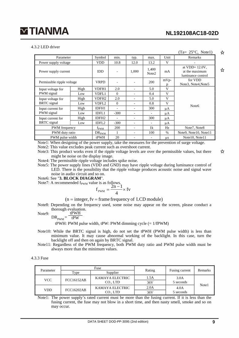
4.3.2 LED driver
(Ta= 25°C, Note1) Parameter Symbol min. typ. max. Unit Remarks
Power supply voltage VDD 10.8 12.0 13.2 V -
Power supply current IDD - 1,000 1,400 Note2 mA
at VDD= 12.0V, at the maximum
luminance control
Permissible ripple voltage VRPD - - 200 mVp-p
for VDD Note3, Note4,Note5
Input voltage for PWM signal
High VDFH1 2.0 - 5.0 V
Note6
Low VDFL1 0 - 0.4 V Input voltage for BRTC signal
High VDFH2 2.0 - 5.0 V Low VDFL2 0 - 0.8 V
Input current for PWM signal
High IDFH1 - - 300 µΑ Low IDFL1 -300 - - µΑ
Input current for BRTC signal
High IDFH2 - - 300 µΑ Low IDFL2 -300 - - µΑ
PWM frequency fPWM 200 - 1k Hz Note7, Note8 PWM duty ratio DRPWM 1 - 100 % Note9, Note10, Note11
PWM pulse width tPWH 20 - - µs Note10, Note11 Note1: When designing of the power supply, take the measures for the prevention of surge voltage. Note2: This value excludes peak current such as overshoot current. Note3: This product works even if the ripple voltage levels are over the permissible values, but there
might be noise on the display image. Note4: The permissible ripple voltage includes spike noise. Note5: The power supply lines (VDD and GND) may have ripple voltage during luminance control of
LED. There is the possibility that the ripple voltage produces acoustic noise and signal wave noise in audio circuit and so on.
Note6: See "3. BLOCK DIAGRAM". Note7: A recommended fPWM value is as follows. Note8: Depending on the frequency used, some noise may appear on the screen, please conduct a
thorough evaluation. Note9: Note10: While the BRTC signal is high, do not set the tPWH (PWM pulse width) is less than
minimum value. It may cause abnormal working of the backlight. In this case, turn the backlight off and then on again by BRTC signal.
Note11: Regardless of the PWM frequency, both PWM duty ratio and PWM pulse width must be always more than the minimum values.
4.3.3 Fuse
Parameter Fuse Rating Fusing current Remarks Type Supplier
VCC FCC16152AB KAMAYA ELECTRIC CO., LTD
1.5A 3.0A 5 seconds
Note1 36V
VDD FCC16202AB KAMAYA ELECTRIC CO., LTD
2.0A 4.0A 5 seconds 36V
Note1: The power supply’s rated current must be more than the fusing current. If it is less than the fusing current, the fuse may not blow in a short time, and then nasty smell, smoke and so on may occur.
module) LCD offrequency frame fv integer,(n
fv4
12nfPWM
==
×−
=
tPWH: PWM pulse width, tPW: PWM dimming cycle (= 1/fPWM) DRPWM =
tPWH tPW
NL192108AC18-02D
DATA SHEET DOD-PP-3095 (2nd edition) 10 10 10
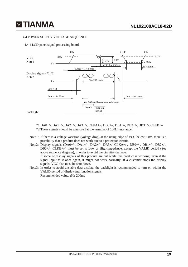
4.4 POWER SUPPLY VOLTAGE SEQUENCE
4.4.1 LCD panel signal processing board
*1 DA0+/-, DA1+/-, DA2+/-, DA3+/-, CLKA+/-, DB0+/-, DB1+/-, DB2+/-, DB3+/-, CLKB+/- *2 These signals should be measured at the terminal of 100Ω resistance.
Note1: If there is a voltage variation (voltage drop) at the rising edge of VCC below 3.0V, there is a
possibility that a product does not work due to a protection circuit. Note2: Display signals (DA0+/-, DA1+/-, DA2+/-, DA3+/-,CLKA+/-, DB0+/-, DB1+/-, DB2+/-,
DB3+/-, CLKB+/-) must be set to Low or High-impedance, except the VALID period (See above sequence diagram), in order to avoid the circuitry damage.
If some of display signals of this product are cut while this product is working, even if the signal input to it once again, it might not work normally. If a customer stops the display signals, VCC also must be shut down.
Note3: In order to avoid unstable data display, the backlight is recommended to turn on within the VALID period of display and function signals. Recommended value: t6 ≥ 200ms
Backlight
0ms < t3
0ms < t4< 35ms
500µs < t1 < 50ms
VALID period
3.0V
0V VCC Note1
t2 > 50ms
0V
3.0V
Display signals *1,*2 Note2
ON OFF ON
0ms < t5 < 35ms
0.3V 2.7V 3.0V VCC dip < 50ms
Turn-on period
t6 ≥ 200ms (Recommended value) Note3
NL192108AC18-02D
DATA SHEET DOD-PP-3095 (2nd edition) 11 11 11
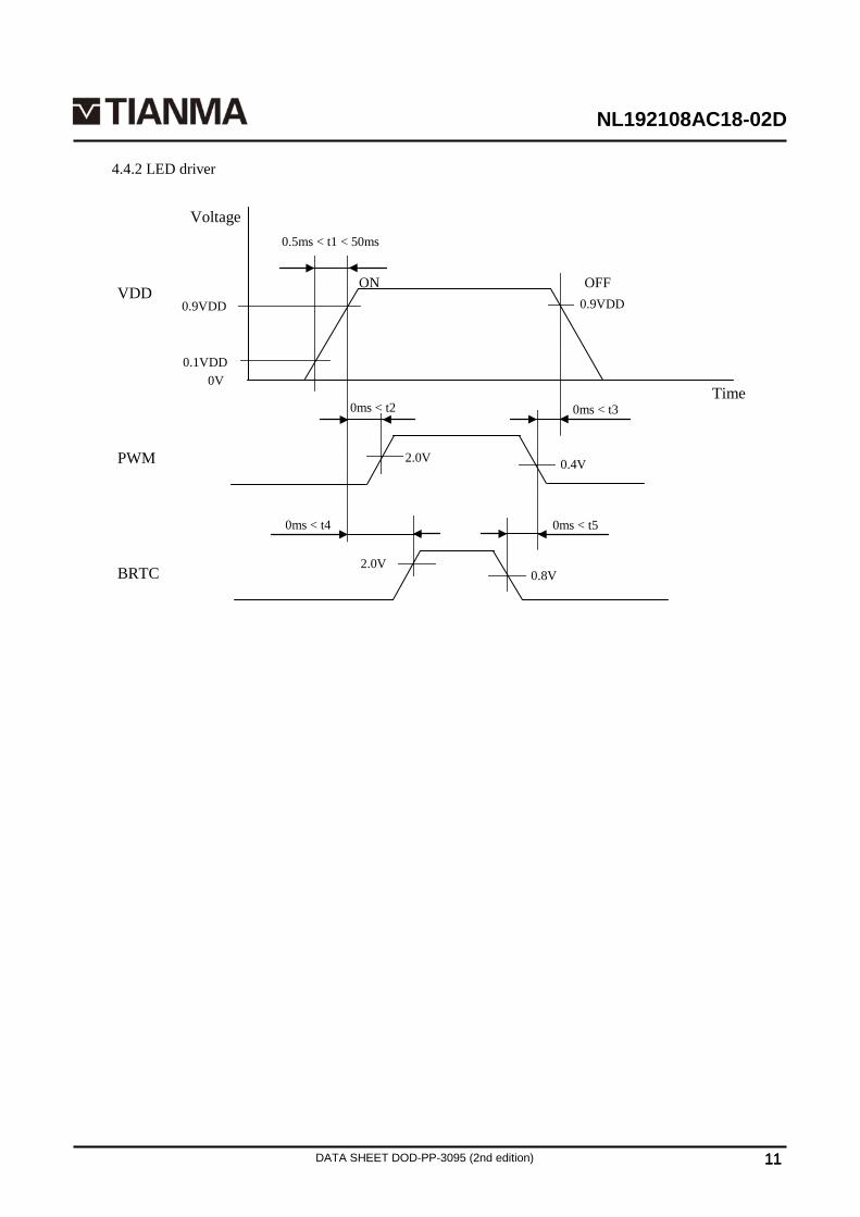
4.4.2 LED driver
ON OFF 0.9VDD 0.9VDD
0.1VDD
VDD
Voltage
Time 0V
PWM
BRTC
0.5ms < t1 < 50ms
0ms < t3 0ms < t2
0ms < t4 0ms < t5
2.0V
2.0V 0.8V
0.4V
NL192108AC18-02D
DATA SHEET DOD-PP-3095 (2nd edition) 12 12 12
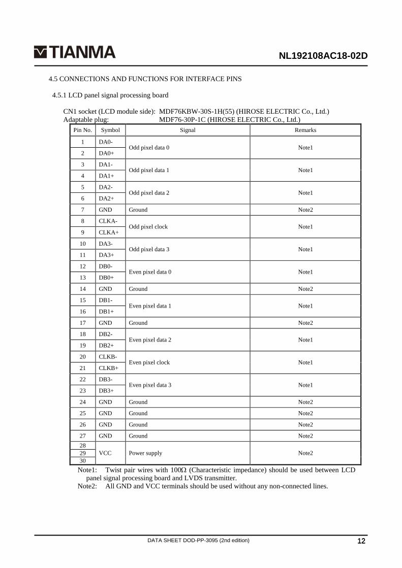
4.5 CONNECTIONS AND FUNCTIONS FOR INTERFACE PINS
4.5.1 LCD panel signal processing board
CN1 socket (LCD module side): MDF76KBW-30S-1H(55) (HIROSE ELECTRIC Co., Ltd.) Adaptable plug: MDF76-30P-1C (HIROSE ELECTRIC Co., Ltd.)
Pin No. Symbol Signal Remarks
1 DA0- Odd pixel data 0 Note1
2 DA0+
3 DA1- Odd pixel data 1 Note1
4 DA1+
5 DA2- Odd pixel data 2 Note1
6 DA2+
7 GND Ground Note2
8 CLKA- Odd pixel clock Note1
9 CLKA+
10 DA3- Odd pixel data 3 Note1
11 DA3+
12 DB0- Even pixel data 0 Note1
13 DB0+
14 GND Ground Note2
15 DB1- Even pixel data 1 Note1
16 DB1+
17 GND Ground Note2
18 DB2- Even pixel data 2 Note1
19 DB2+
20 CLKB- Even pixel clock Note1
21 CLKB+
22 DB3- Even pixel data 3 Note1
23 DB3+
24 GND Ground Note2
25 GND Ground Note2
26 GND Ground Note2
27 GND Ground Note2 28
VCC Power supply Note2 29 30
Note1: Twist pair wires with 100Ω (Characteristic impedance) should be used between LCD panel signal processing board and LVDS transmitter.
Note2: All GND and VCC terminals should be used without any non-connected lines.
NL192108AC18-02D
DATA SHEET DOD-PP-3095 (2nd edition) 13 13 13
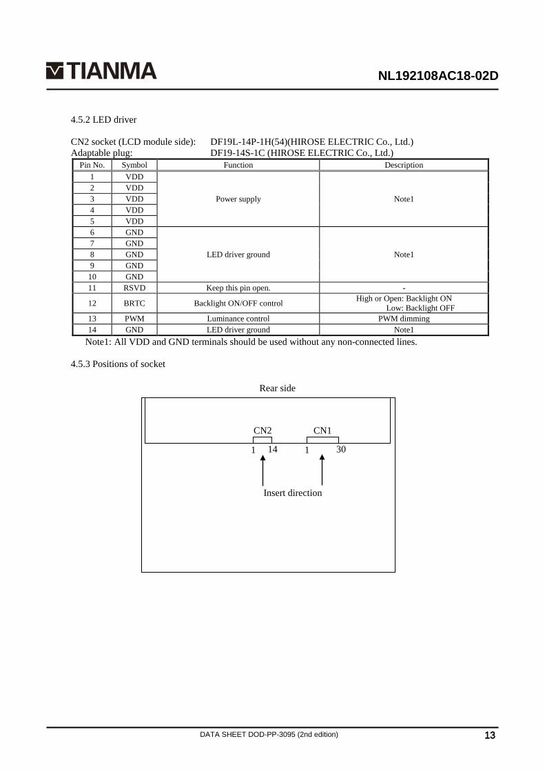
4.5.2 LED driver
CN2 socket (LCD module side): DF19L-14P-1H(54)(HIROSE ELECTRIC Co., Ltd.) Adaptable plug: DF19-14S-1C (HIROSE ELECTRIC Co., Ltd.)
Pin No. Symbol Function Description 1 VDD
Power supply Note1 2 VDD 3 VDD 4 VDD 5 VDD 6 GND
LED driver ground Note1 7 GND 8 GND 9 GND
10 GND 11 RSVD Keep this pin open. -
12 BRTC Backlight ON/OFF control High or Open: Backlight ON Low: Backlight OFF
13 PWM Luminance control PWM dimming 14 GND LED driver ground Note1
Note1: All VDD and GND terminals should be used without any non-connected lines.
4.5.3 Positions of socket
Rear side
CN1
30 1
CN2
14 1
Insert direction
NL192108AC18-02D
DATA SHEET DOD-PP-3095 (2nd edition) 14 14 14
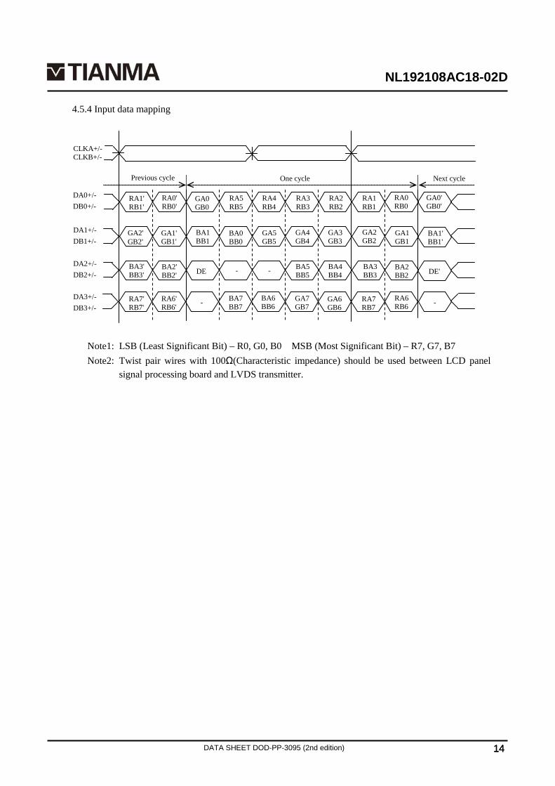
4.5.4 Input data mapping
Note1: LSB (Least Significant Bit) – R0, G0, B0 MSB (Most Significant Bit) – R7, G7, B7 Note2: Twist pair wires with 100Ω(Characteristic impedance) should be used between LCD panel
signal processing board and LVDS transmitter.
RA0 RB0
RA1 RB1
RA2 RB2
RA3 RB3
RA4 RB4
RA5 RB5
GA0 GB0
GA1 GB1
GA2 GB2
GA3 GB3
GA4 GB4
GA5 GB5
BA0 BB0
BA1 BB1
CLKA+/- CLKB+/-
DA0+/- DB0+/-
BA2 BB2
BA3 BB3
BA4 BB4
BA5 BB5 DE
One cycle
RA6 RB6
RA7 RB7
GA6 GB6
GA7 GB7
BA6 BB6
BA7 BB7
RA0'RB0'
RA1' RB1'
GA1' GB1'
GA2' GB2'
BA2' BB2'
BA3' BB3'
RA6' RB6'
RA7' RB7'
-
GA0' GB0'
BA1' BB1'
DE'
Previous cycle Next cycle
- -
-
DA1+/- DB1+/-
DA2+/- DB2+/-
DA3+/- DB3+/-
NL192108AC18-02D
DATA SHEET DOD-PP-3095 (2nd edition) 15 15 15
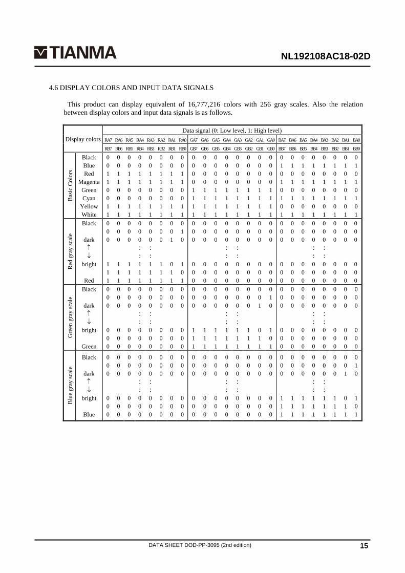
4.6 DISPLAY COLORS AND INPUT DATA SIGNALS
This product can display equivalent of 16,777,216 colors with 256 gray scales. Also the relation between display colors and input data signals is as follows.
Display colors Data signal (0: Low level, 1: High level)
RA7 RA6 RA5 RA4 RA3 RA2 RA1 RA0 GA7 GA6 GA5 GA4 GA3 GA2 GA1 GA0 BA7 BA6 BA5 BA4 BA3 BA2 BA1 BA0
RB7 RB6 RB5 RB4 RB3 RB2 RB1 RB0 GB7 GB6 GB5 GB4 GB3 GB2 GB1 GB0 BB7 BB6 BB5 BB4 BB3 BB2 BB1 BB0
Bas
ic C
olor
s
Black Blue Red
Magenta Green Cyan
Yellow White
0 0 1 1 0 0 1 1
0 0 1 1 0 0 1 1
0 0 1 1 0 0 1 1
0 0 1 1 0 0 1 1
0 0 1 1 0 0 1 1
0 0 1 1 0 0 1 1
0 0 1 1 0 0 1 1
0 0 1 1 0 0 1 1
0 0 0 0 1 1 1 1
0 0 0 0 1 1 1 1
0 0 0 0 1 1 1 1
0 0 0 0 1 1 1 1
0 0 0 0 1 1 1 1
0 0 0 0 1 1 1 1
0 0 0 0 1 1 1 1
0 0 0 0 1 1 1 1
0 1 0 1 0 1 0 1
0 1 0 1 0 1 0 1
0 1 0 1 0 1 0 1
0 1 0 1 0 1 0 1
0 1 0 1 0 1 0 1
0 1 0 1 0 1 0 1
0 1 0 1 0 1 0 1
0 1 0 1 0 1 0 1
Red
gra
y sc
ale
Black
dark ↑ ↓
bright
Red
0 0 0
1 1 1
0 0 0
1 1 1
0 0 0
1 1 1
0 0 0 : : 1 1 1
0 0 0 : : 1 1 1
0 0 0
1 1 1
0 0 1
0 1 1
0 1 0
1 0 1
0 0 0
0 0 0
0 0 0 0 0 0
0 0 0 0 0 0
0 0 0 : : 0 0 0
0 0 0 : : 0 0 0
0 0 0
0 0 0
0 0 0
0 0 0
0 0 0
0 0 0
0 0 0
0 0 0
0 0 0
0 0 0
0 0 0
0 0 0
0 0 0 : : 0 0 0
0 0 0 : : 0 0 0
0 0 0
0 0 0
0 0 0
0 0 0
0 0 0
0 0 0
Gre
en g
ray
scal
e
Black
dark ↑ ↓
bright
Green
0 0 0
0 0 0
0 0 0
0 0 0
0 0 0
0 0 0
0 0 0 : : 0 0 0
0 0 0 : : 0 0 0
0 0 0
0 0 0
0 0 0
0 0 0
0 0 0
0 0 0
0 0 0
1 1 1
0 0 0 1 1 1
0 0 0 1 1 1
0 0 0 : : 1 1 1
0 0 0 : : 1 1 1
0 0 0
1 1 1
0 0 1
0 1 1
0 1 0
1 0 1
0 0 0
0 0 0
0 0 0
0 0 0
0 0 0
0 0 0
0 0 0 : : 0 0 0
0 0 0 : : 0 0 0
0 0 0
0 0 0
0 0 0
0 0 0
0 0 0
0 0 0
Blu
e gr
ay sc
ale
Black
dark ↑ ↓
bright
Blue
0 0 0
0 0 0
0 0 0
0 0 0
0 0 0
0 0 0
0 0 0 : : 0 0 0
0 0 0 : : 0 0 0
0 0 0
0 0 0
0 0 0
0 0 0
0 0 0
0 0 0
0 0 0
0 0 0
0 0 0 0 0 0
0 0 0 0 0 0
0 0 0 : : 0 0 0
0 0 0 : : 0 0 0
0 0 0
0 0 0
0 0 0
0 0 0
0 0 0
0 0 0
0 0 0
1 1 1
0 0 0
1 1 1
0 0 0
1 1 1
0 0 0 : : 1 1 1
0 0 0 : : 1 1 1
0 0 0
1 1 1
0 0 1
0 1 1
0 1 0
1 0 1
NL192108AC18-02D
DATA SHEET DOD-PP-3095 (2nd edition) 16 16 16
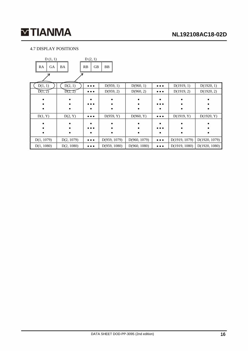
4.7 DISPLAY POSITIONS
D (1, 1) D (2, 1)
RA GA BA RB GB BB
D(1, 1) D(2, 1) • • • D(959, 1) D(960, 1) • • • D(1919, 1) D(1920, 1) D(1, 2) D(2, 2) • • • D(959, 2) D(960, 2) • • • D(1919, 2) D(1920, 2)
• • •
• • •
• • • •
•
• • •
• • •
• • • •
•
• • •
• • •
D(1, Y) D(2, Y) • • • D(959, Y) D(960, Y) • • • D(1919, Y) D(1920, Y)
• • •
• • •
• • • •
•
• • •
• • •
• • • •
•
• • •
• • •
D(1, 1079) D(2, 1079) • • • D(959, 1079) D(960, 1079) • • • D(1919, 1079) D(1920, 1079) D(1, 1080) D(2, 1080) • • • D(959, 1080) D(960, 1080) • • • D(1919, 1080) D(1920, 1080)
NL192108AC18-02D
DATA SHEET DOD-PP-3095 (2nd edition) 17 17 17
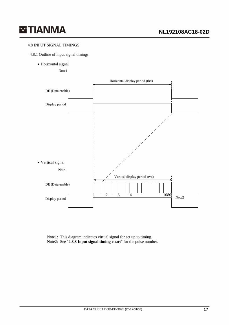
4.8 INPUT SIGNAL TIMINGS
4.8.1 Outline of input signal timings
• Horizontal signal • Vertical signal
Note1: This diagram indicates virtual signal for set up to timing. Note2: See "4.8.3 Input signal timing chart" for the pulse number.
Display period
Horizontal display period (thd)
DE (Data enable)
Note1
Vertical display period (tvd)
1 2 3 4 1080 Display period
DE (Data enable)
Note2
Note1
NL192108AC18-02D
DATA SHEET DOD-PP-3095 (2nd edition) 18 18 18
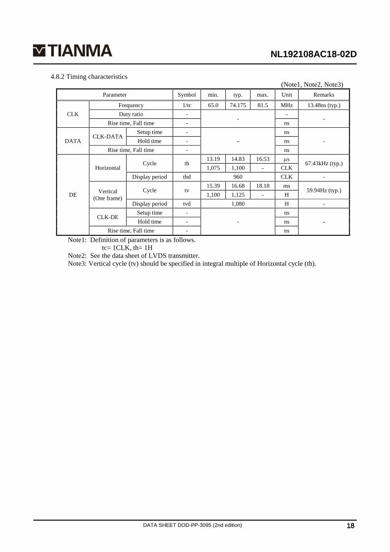
4.8.2 Timing characteristics
(Note1, Note2, Note3) Parameter Symbol min. typ. max. Unit Remarks
CLK Frequency 1/tc 65.0 74.175 81.5 MHz 13.48ns (typ.) Duty ratio -
- - -
Rise time, Fall time - ns
DATA CLK-DATA Setup time - -
ns - Hold time - ns
Rise time, Fall time - ns
DE
Horizontal Cycle th 13.19 14.83 16.53 µs 67.43kHz (typ.)
1,075 1,100 - CLK Display period thd 960 CLK -
Vertical (One frame)
Cycle tv 15.39 16.68 18.18 ms 59.94Hz (typ.)
1,100 1,125 - H Display period tvd 1,080 H -
CLK-DE Setup time - -
ns - Hold time - ns
Rise time, Fall time - ns Note1: Definition of parameters is as follows.
tc= 1CLK, th= 1H Note2: See the data sheet of LVDS transmitter. Note3: Vertical cycle (tv) should be specified in integral multiple of Horizontal cycle (th).
NL192108AC18-02D
DATA SHEET DOD-PP-3095 (2nd edition) 19 19 19
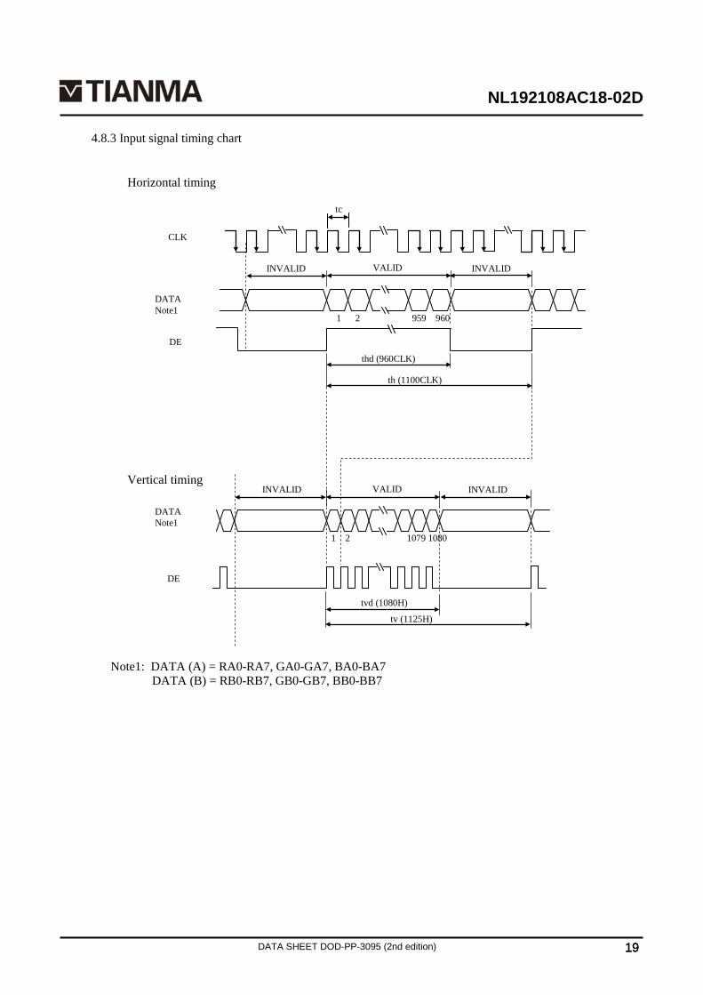
4.8.3 Input signal timing chart
Note1: DATA (A) = RA0-RA7, GA0-GA7, BA0-BA7 DATA (B) = RB0-RB7, GB0-GB7, BB0-BB7
Horizontal timing
INVALID
CLK
DE
DATA Note1
INVALID
thd (960CLK)
th (1100CLK)
DE
Vertical timing
tvd (1080H) tv (1125H)
tc
DATA Note1
INVALID
INVALID VALID
VALID
1 2 1079 1080
1 2 959 960
NL192108AC18-02D
DATA SHEET DOD-PP-3095 (2nd edition) 20 20 20
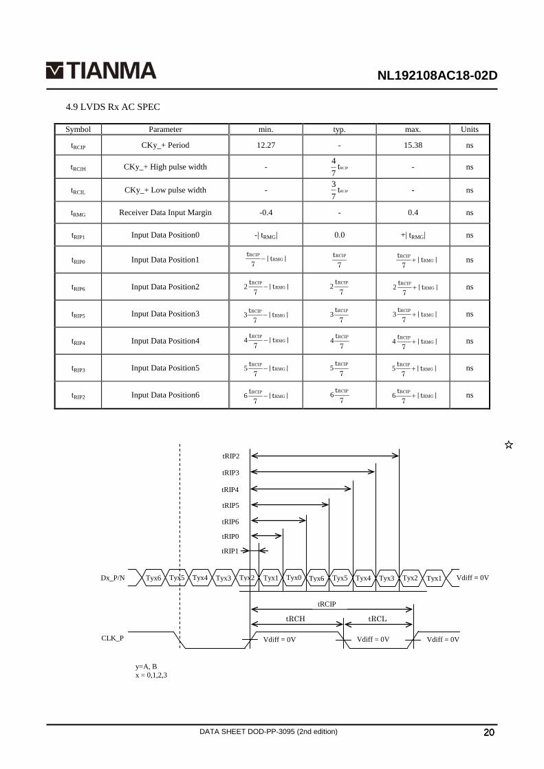
4.9 LVDS Rx AC SPEC
Symbol Parameter min. typ. max. Units
tRCIP CKy_+ Period 12.27 - 15.38 ns
tRCIH CKy_+ High pulse width - RCIPt74 - ns
tRCIL CKy_+ Low pulse width - RCIPt73 - ns
tRMG Receiver Data Input Margin -0.4 - 0.4 ns
tRIP1 Input Data Position0 -| tRMG| 0.0 +| tRMG| ns
tRIP0 Input Data Position1
ns
tRIP6 Input Data Position2
ns
tRIP5 Input Data Position3
ns
tRIP4 Input Data Position4
ns
tRIP3 Input Data Position5
ns
tRIP2 Input Data Position6
ns
|t|7
tRMG
RCIP− |t|
7t
RMGRCIP
+
|t|7
tRMG
RCIP−2
7tRCIP2 |t|
7t
RMGRCIP
+2
|t|7
tRMG
RCIP−3
7tRCIP3 ||t
7t
RMGRCIP
+3
|t|7
tRMG
RCIP−4
7tRCIP4 |t|
7t
RMGRCIP
+4
||t7
tRMG
RCIP−6 7
tRCIP6 ||t7
tRMG
RCIP+6
||t7
tRMG
RCIP−5
7tRCIP5 ||t
7t
RMGRCIP
+5
7tRCIP
tRCH tRCL
CLK_P
Dx_P/N Vdiff = 0V Tyx5
Vdiff = 0V Vdiff = 0V Vdiff = 0V
tRCIP
Tyx6 Tyx4 Tyx3 Tyx2 Tyx1 Tyx0
y=A, B x = 0,1,2,3
Tyx5 Tyx6 Tyx4 Tyx3 Tyx2 Tyx1
tRIP1
tRIP0
tRIP6
tRIP5
tRIP4
tRIP3
tRIP2
NL192108AC18-02D
DATA SHEET DOD-PP-3095 (2nd edition) 21 21 21
4.10 OPTICS
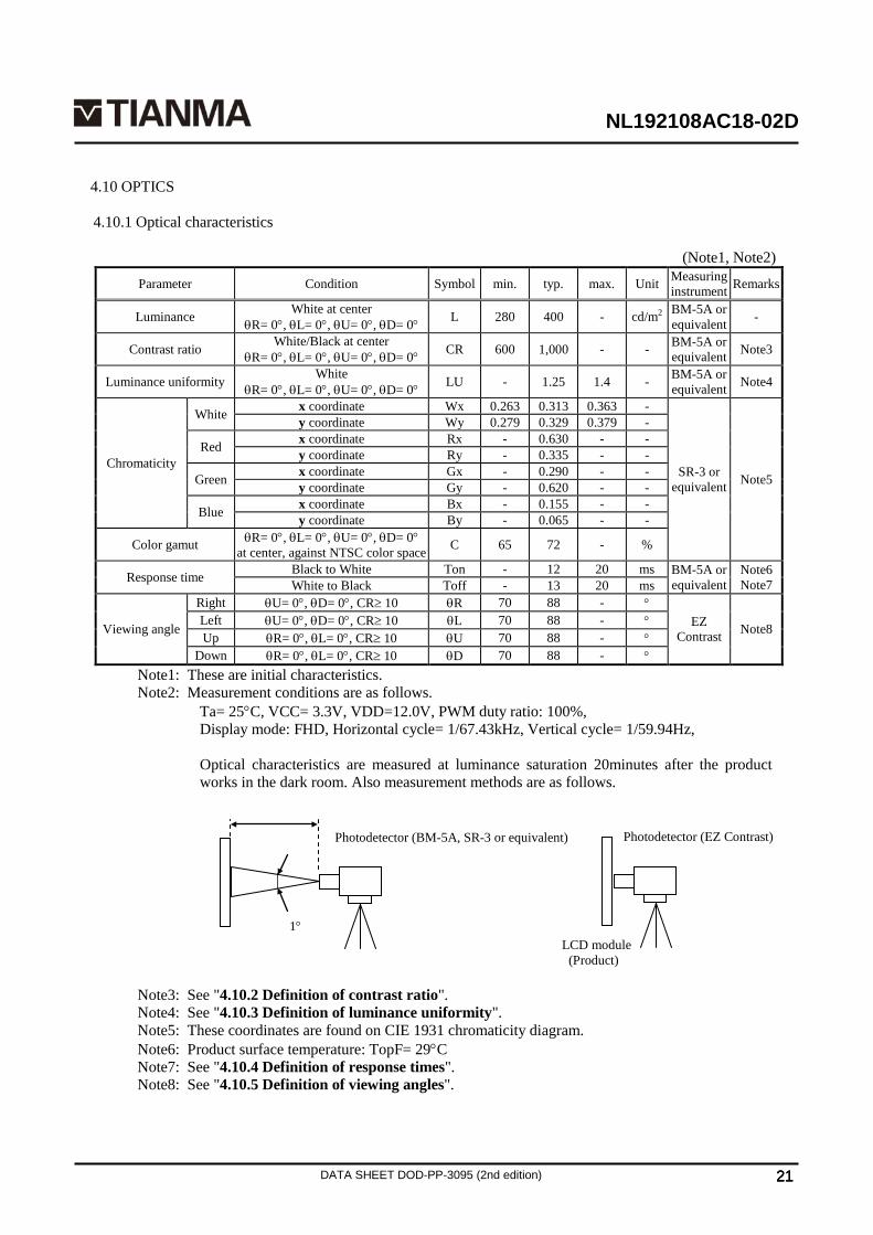
4.10.1 Optical characteristics
(Note1, Note2)
Parameter Condition Symbol min. typ. max. Unit Measuring instrument Remarks
Luminance White at center θR= 0°, θL= 0°, θU= 0°, θD= 0° L 280 400 - cd/m2 BM-5A or
equivalent -
Contrast ratio White/Black at center θR= 0°, θL= 0°, θU= 0°, θD= 0° CR 600 1,000 - - BM-5A or
equivalent Note3
Luminance uniformity White θR= 0°, θL= 0°, θU= 0°, θD= 0° LU - 1.25 1.4 - BM-5A or
equivalent Note4
Chromaticity
White x coordinate Wx 0.263 0.313 0.363 -
SR-3 or equivalent Note5
y coordinate Wy 0.279 0.329 0.379 -
Red x coordinate Rx - 0.630 - - y coordinate Ry - 0.335 - -
Green x coordinate Gx - 0.290 - - y coordinate Gy - 0.620 - -
Blue x coordinate Bx - 0.155 - - y coordinate By - 0.065 - -
Color gamut θR= 0°, θL= 0°, θU= 0°, θD= 0° at center, against NTSC color space C 65 72 - %
Response time Black to White Ton - 12 20 ms BM-5A or equivalent
Note6 Note7 White to Black Toff - 13 20 ms
Viewing angle
Right θU= 0°, θD= 0°, CR≥ 10 θR 70 88 - ° EZ
Contrast Note8 Left θU= 0°, θD= 0°, CR≥ 10 θL 70 88 - ° Up θR= 0°, θL= 0°, CR≥ 10 θU 70 88 - °
Down θR= 0°, θL= 0°, CR≥ 10 θD 70 88 - ° Note1: These are initial characteristics. Note2: Measurement conditions are as follows.
Ta= 25°C, VCC= 3.3V, VDD=12.0V, PWM duty ratio: 100%, Display mode: FHD, Horizontal cycle= 1/67.43kHz, Vertical cycle= 1/59.94Hz, Optical characteristics are measured at luminance saturation 20minutes after the product works in the dark room. Also measurement methods are as follows.
Note3: See "4.10.2 Definition of contrast ratio". Note4: See "4.10.3 Definition of luminance uniformity". Note5: These coordinates are found on CIE 1931 chromaticity diagram. Note6: Product surface temperature: TopF= 29°C Note7: See "4.10.4 Definition of response times". Note8: See "4.10.5 Definition of viewing angles".
1°
Photodetector (BM-5A, SR-3 or equivalent)
Photodetector (EZ Contrast)
LCD module (Product)
NL192108AC18-02D
DATA SHEET DOD-PP-3095 (2nd edition) 22 22 22
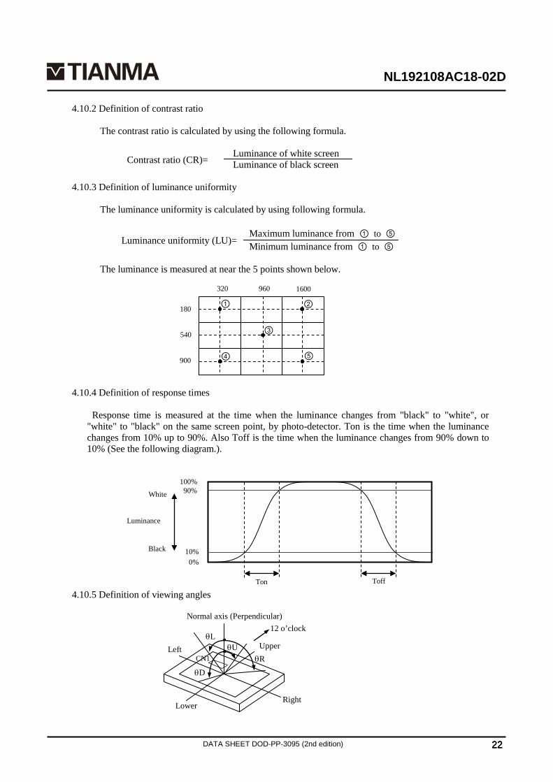
4.10.2 Definition of contrast ratio
The contrast ratio is calculated by using the following formula.
Luminance of white screen Luminance of black screen
4.10.3 Definition of luminance uniformity
The luminance uniformity is calculated by using following formula.
Maximum luminance from ① to ⑤ Minimum luminance from ① to ⑤
The luminance is measured at near the 5 points shown below.
4.10.4 Definition of response times
Response time is measured at the time when the luminance changes from "black" to "white", or "white" to "black" on the same screen point, by photo-detector. Ton is the time when the luminance changes from 10% up to 90%. Also Toff is the time when the luminance changes from 90% down to 10% (See the following diagram.).
4.10.5 Definition of viewing angles
Contrast ratio (CR)=
Luminance uniformity (LU)=
③
④ ⑤
① ② 320 960 1600
180
540
900
Left Upper
Lower
Normal axis (Perpendicular)
θU
θD θR
θL 12 o’clock
Right
CN1
100% 90%
10% 0%
Ton Toff
Luminance
White
Black
NL192108AC18-02D
DATA SHEET DOD-PP-3095 (2nd edition) 23 23 23
5. ESTIMATED LUMINANCE LIFETIME
The luminance lifetime is the time from initial luminance to half-luminance.
This lifetime is the estimated value, and is not guarantee value.
Condition Estimated luminance lifetime
(Life time expectancy) Note1, Note2, Note3
Unit
LED elementary substance
25°C (Ambient temperature of the product) Continuous operation, PWM duty ratio:100% 50,000
h 70°C (Temperature of LCD panel surface
and rear shield surface) Continuous operation, PWM duty ratio:100%
30,000
Note1: Life time expectancy is mean time to half-luminance. Note2: Estimated luminance lifetime is not the value for LCD module but the value for LED
elementary substance. Note3: By ambient temperature, the lifetime changes particularly. Especially, in case the product
works under high temperature environment, the lifetime becomes short.
NL192108AC18-02D
DATA SHEET DOD-PP-3095 (2nd edition) 24 24 24
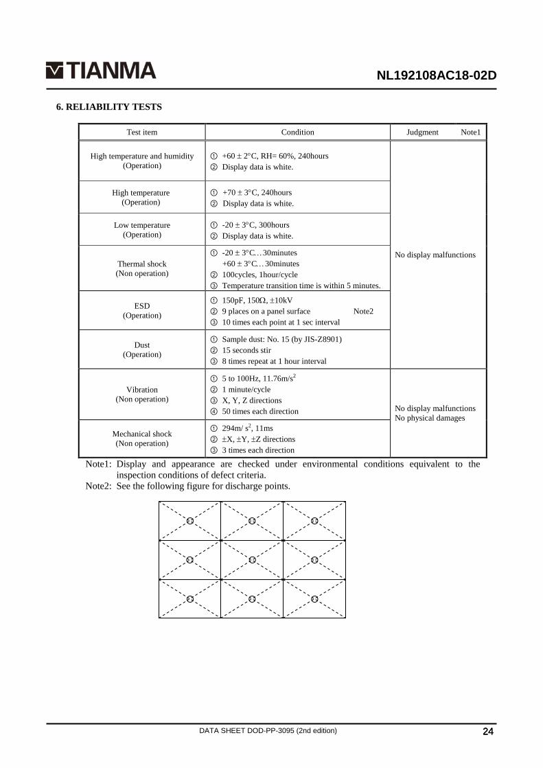
6. RELIABILITY TESTS
Test item Condition Judgment Note1
High temperature and humidity (Operation)
① +60 ± 2°C, RH= 60%, 240hours ② Display data is white.
No display malfunctions
High temperature (Operation)
① +70 ± 3°C, 240hours ② Display data is white.
Low temperature (Operation)
① -20 ± 3°C, 300hours ② Display data is white.
Thermal shock (Non operation)
① -20 ± 3°C…30minutes +60 ± 3°C…30minutes
② 100cycles, 1hour/cycle ③ Temperature transition time is within 5 minutes.
ESD (Operation)
① 150pF, 150Ω, ±10kV ② 9 places on a panel surface Note2 ③ 10 times each point at 1 sec interval
Dust (Operation)
① Sample dust: No. 15 (by JIS-Z8901) ② 15 seconds stir ③ 8 times repeat at 1 hour interval
Vibration (Non operation)
① 5 to 100Hz, 11.76m/s2 ② 1 minute/cycle ③ X, Y, Z directions ④ 50 times each direction No display malfunctions
No physical damages
Mechanical shock (Non operation)
① 294m/ s2, 11ms ② ±X, ±Y, ±Z directions ③ 3 times each direction
Note1: Display and appearance are checked under environmental conditions equivalent to the inspection conditions of defect criteria.
Note2: See the following figure for discharge points.

NL192108AC18-02D
DATA SHEET DOD-PP-3095 (2nd edition) 25 25 25
7. PRECAUTIONS
7.1 MEANING OF CAUTION SIGNS
The following caution signs have very important meaning. Be sure to read "7.2 CAUTIONS" and
"7.3 ATTENTIONS"!
! This sign has the meaning that a customer will be injured or the product will sustain
damage if the customer practices wrong operations.
This sign has the meaning that a customer will be injured if the customer practices
wrong operations.
7.2 CAUTIONS
∗ Do not shock and press the LCD panel and the backlight! There is a danger of breaking,
because they are made of glass. (Shock: Equal to or no greater than 294m/s2 and equal to or no greater than 11ms, Pressure: Equal to or no greater than 19.6 N (φ16mm jig))
7.3 ATTENTIONS
7.3.1 Handling of the product
① Take hold of both ends without touching the circuit board when the product (LCD module) is picked up from inner packing box to avoid broken down or misadjustment, because of stress to mounting parts on the circuit board.
② Do not hook nor pull cables such as lamp cable, and so on, in order to avoid any damage. ③ When the product is put on the table temporarily, display surface must be placed downward. ④ When handling the product, take the measures of electrostatic discharge with such as earth band,
ionic shower and so on, because the product may be damaged by electrostatic. ⑤ The torque for product mounting screws must never exceed 0.230N⋅m. Higher torque might result
in distortion of the bezel. And the length of product mounting screws must be ≤ 2.5mm. ⑥ The product must be installed using mounting holes without undue stress such as bends or twist
(See outline drawings). And do not add undue stress to any portion (such as bezel flat area). Bends or twist described above and undue stress to any portion may cause display mura. Recommended installing method: Ideal plane "A" is defined by one mounting hole (datum point) and other mounting holes. The ideal plane "A" should be the same plane within ±0.3 mm.
!
Product
Mounting hole
Ideal plane "A"
Mounting hole (Datum point) Mounting hole
NL192108AC18-02D
DATA SHEET DOD-PP-3095 (2nd edition) 26 26 26
⑦ Do not press or rub on the sensitive product surface. When cleaning the panel surface, wipe it with
a soft dry cloth. ⑧ Do not push or pull the interface connectors while the product is working. ⑨ When handling the product, use of an original protection sheet on the product surface (polarizer) is
recommended for protection of product surface. Adhesive type protection sheet may change color or characteristics of the polarizer.
⑩ Usually liquid crystals don't leak through the breakage of glasses because of the surface tension of thin layer and the construction of LCD panel. But, if you contact with liquid crystal by any chance, please wash it away with soap and water.
7.3.2 Environment
① Do not operate or store in high temperature, high humidity, dewdrop atmosphere or corrosive
gases. Keep the product in packing box with antistatic pouch in room temperature to avoid dusts and sunlight, when storing the product.
② In order to prevent dew condensation occurred by temperature difference, the product packing box must be opened after enough time being left under the environment of an unpacking room. Evaluate the storage time sufficiently because dew condensation is affected by the environmental temperature and humidity. (Recommended leaving time: 6 hours or more with the original packing state after a customer receives the package)
③ Do not operate in high magnetic field. If not, circuit boards may be broken. ④ This product is not designed as radiation hardened.
7.3.3 Characteristics
The following items are neither defects nor failures. ① Characteristics of the LCD (such as response time, luminance, color uniformity and so on) may be
changed depending on ambient temperature. If the product is stored under condition of low temperature for a long time, it may cause display mura. In this case, the product should be operated after enough time being left under condition of operating temperature.
② Display mura, flickering, vertical streams or tiny spots may be observed depending on display patterns.
③ Do not display the fixed pattern for a long time because it may cause image sticking. Use a screen saver, if the fixed pattern is displayed on the screen.
④ The display color may be changed depending on viewing angle because of the use of condenser sheet in the backlight.
⑤ Optical characteristics may be changed depending on input signal timings. ⑥ The interference noise between input signal frequency for this product's signal processing board
and luminance control frequency of backlight driving circuit may appear on a display. Set up luminance control frequency of backlight driving circuit so that the interference noise does not appear.

NL192108AC18-02D
DATA SHEET DOD-PP-3095 (2nd edition) 27 27 27
7.3.4 Others
① All GND, VCC and VDD terminals should be used without any non-connected lines. ② Do not disassemble a product or adjust variable resistors. ③ Pack the product with the original shipping package, in order to avoid any damages during
transportation, when returning the product to TMJ. ④ The information of China RoHS (Ⅱ) six hazardous substances or elements in this product is as
follows. China RoHS (Ⅱ) six hazardous substances or elements
Lead (Pb)
Mercury (Hg)
Cadmium (Cd)
Hexavalent Chromium
(Cr VI)
Polybrominated Biphenys
(PBB)
Polybrominated Biphenyl Ethers
(PBDE)
⃝ ⃝ ⃝ ⃝ ⃝
Note1: ⃝: This indicates that the poisonous or harmful material in all the homogeneous materials for this part is equal or below the limitation level of GB/T26572-2011 standard regulation.
: This indicates that the poisonous or harmful material in all the homogeneous materials for this part is above the limitation level of GB/T26572-2011 standard regulation.

NL192108AC18-02D
DATA SHEET DOD-PP-3095 (2nd edition) 28
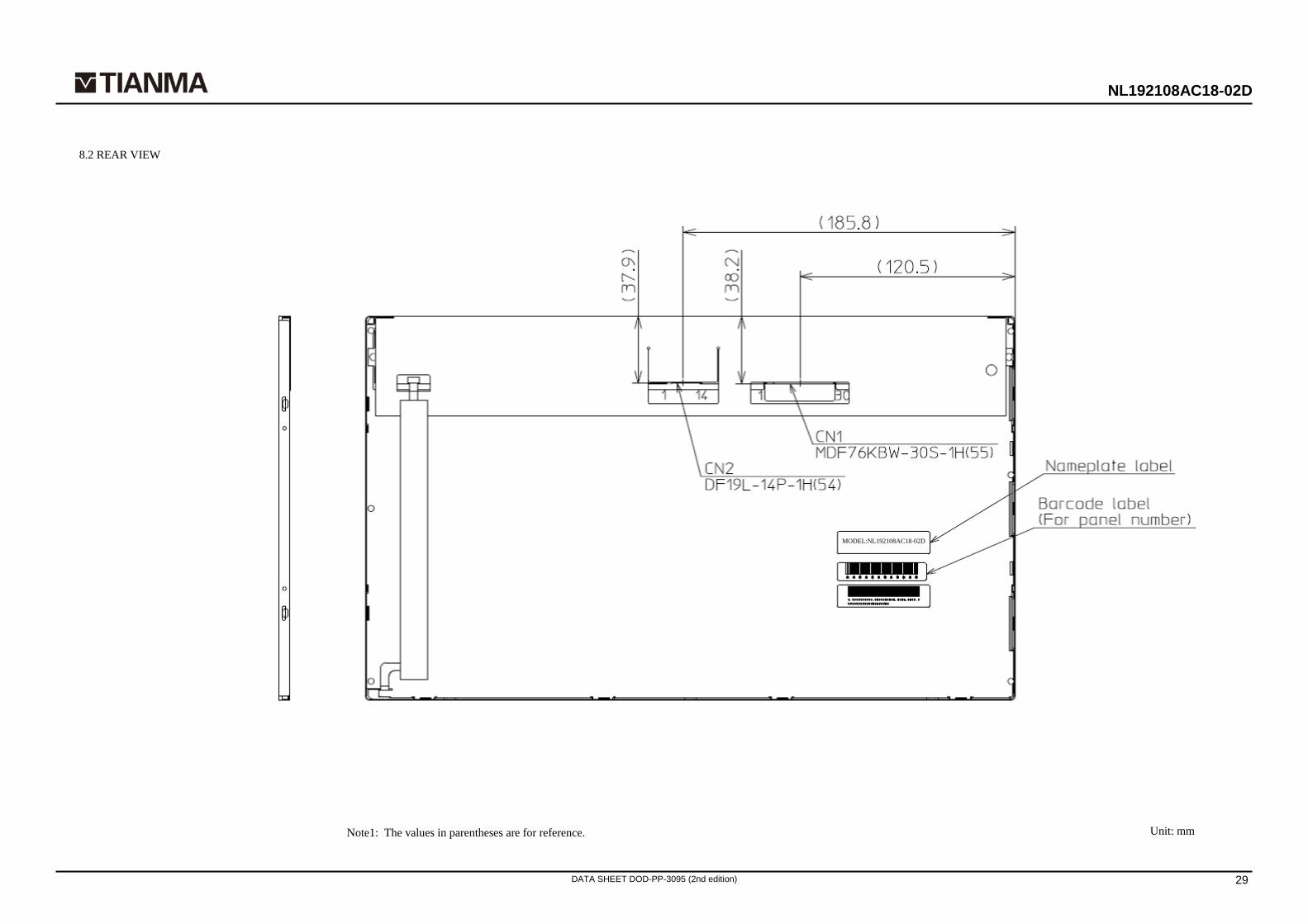
8. OUTLINE DRAWINGS
8.1 FRONT VIEW
Unit: mm
Note1: The values in parentheses are for reference. Note2: The torque for product mounting screws must never exceed 0.230N⋅m. And the length of product mounting screws must be ≤ 2.5mm.
NL192108AC18-02D
DATA SHEET DOD-PP-3095 (2nd edition) 29
8.2 REAR VIEW
Unit: mm
Note1: The values in parentheses are for reference.
MODEL:NL192108AC18-02D
NL192108AC18-02D
DATA SHEET DOD-PP-3095 (2nd edition) 30 30 30
REVISION HISTORY
The inside of latest specifications is revised to the clerical error and the major improvement of previous
edition. Only a changed part such as functions, characteristic value and so on that may affect a design of customers, are described especially below.
Edition Documen
t number Prepared
date Revision contents and signature
1st edition
DOD-PP- 2571
Mar.28, 2017
Revision contents PRELIMINARY DATA SHEET DOD-PP-2509(5) → DATA SHEET DOD-PP-2571(1) P4 Outline - Features
• Acquisition product for UL60950-1/CSA C22.2 No.60950-1-03 (File number: E170632) (addition) • Compliance with the European RoHS directive (2011/65/EU) (addition)
P26 Attentions - Others • ④ (addition)
P28 Outline Drawings – REAR VIEW • Addition of slit on barrier (correction)
2nd edition
DOD-PP- 3095
Apr. 17, 2019
Revision contents CORRECTION OF DESCRIPTIVE CONTENTS
• Change of company name P4 Outline - Features
• High resolution (addition) • Wide temperature range (elimination) • Narrow frame → Narrow border (Revised)
P7 Detailed specifications – Absolute maximum ratings • Function signal for LED driver → LED driver (Revised)
P8 Electrical characteristics - LCD panel signal processing board • Note1 (addition)
P9 Electrical characteristics - LED driver • Note1 (Position correction) • Note3 (elimination) • Power supply current – Remarks: at the maximum luminance control (addition) • Note9 (addition)
P20 LVDS Rx AC SPEC (Revised) P25 Attentions – Handling of the product
• ② (addition) P26Attentions – Handling of the product
• ⑧ → ⑧,⑨ (division) P26 Attentions – Characteristics
• ⑥ (addition)
T.OGAWA Approved by
M.ITO Checked by
Writer
R. KAWASHIMA Prepared by
T. UCHIDA
Approved by
M.ITO
Checked by
Signature of writer
R. KAWASHIMA
Prepared by

Our company network supports you worldwide with offices in Germany, Austria, Switzerland, the UK and the USA. For more information please contact:
Headquarters
Germany
FORTEC Elektronik AG Lechwiesenstr. 9 86899 Landsberg am Lech Phone: +49 8191 91172-0 E-Mail: [email protected] Internet: www.fortecag.de
Fortec Group Members
Austria
FORTEC Elektronik AG Office Vienna Nuschinggasse 12 1230 Wien Phone: +43 1 8673492-0 E-Mail: [email protected] Internet: www.fortec.at
Germany
Distec GmbH Augsburger Str. 2b 82110 Germering Phone: +49 89 894363-0 E-Mail: [email protected] Internet: www.distec.de
Switzerland
ALTRAC AG Bahnhofstraße 3 5436 Würenlos Phone: +41 44 7446111 E-Mail: [email protected] Internet: www.altrac.ch
United Kingdom
Display Technology Ltd. Osprey House, 1 Osprey Court Hichingbrooke Business Park Huntingdon, Cambridgeshire, PE29 6FN Phone: +44 1480 411600 E-Mail: [email protected] Internet: www. displaytechnology.co.uk
USA
Apollo Display Technologies, Corp. 87 Raynor Avenue, Unit 1Ronkonkoma, NY 11779 Phone: +1 631 5804360 E-Mail: [email protected] Internet: www.apollodisplays.com