datasheet - intersil · pdf filedatasheet the icm7243 is an 8-character, alphanumeric ... 34...
TRANSCRIPT
FN3162 Rev 5.00 Page 1 of 17October 2, 2015
FN3162Rev 5.00
October 2, 2015
ICM72438-Character, Microprocessor-Compatible, LED Display Decoder Driver
DATASHEET
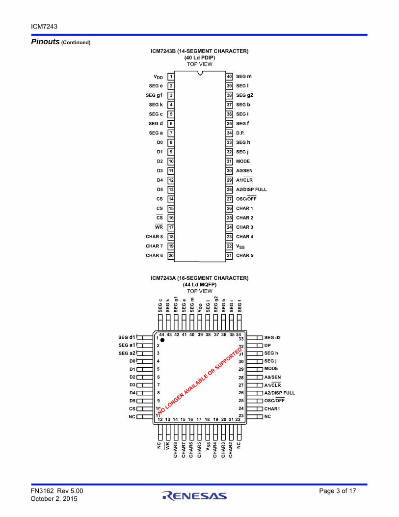
The ICM7243 is an 8-character, alphanumeric display driver and controller which provides all the circuitry required to interface a microprocessor or digital system to a 14-segment or 16-segment display. It is primarily intended for use in microprocessor systems, where it minimizes hardware and software overhead. Incorporated on-chip are a 64-character ASClI decoder, 8x6 memory, high power character and segment drivers, and the multiplex scan circuitry.
6-bit ASCll data to be displayed is written into the memory directly from the microprocessor data bus. Data location depends upon the selection of either Sequential (MODE = 1) or Random access mode (MODE = 0). In the Sequential Access mode the first entry is stored in the lowest location and displayed in the “left-most” character position. Each subsequent entry is automatically stored in the next higher location and displayed to the immediate “right” of the previous entry. A DISPlay FULL signal is provided after 8 entries; this signal can be used for cascading devices together. A CLeaR pin is provided to clear the memory and reset the location counter. The Random Access mode allows the processor to select the memory address and display digit for each input word.
The character multiplex scan runs whenever data is not being entered. It scans the memory and CHARacter drivers, and ensures that the decoding from memory to display is done in the proper sequence. Intercharacter blanking is provided to avoid display ghosting
Features
• 14-Segment and 16-Segment Fonts with Decimal Point
• Mask Programmable for Other Font-Sets Up to 64 Characters
• Microprocessor Compatible
• Directly Drives LED Common Cathode Displays
• Cascadable Without Additional Hardware
• Standby Feature Turns Display Off; Puts Chip in Low Power Mode
• Sequential Entry or Random Entry of Data Into Display
• Single +5V Operation
• Character and Segment Drivers, All MUX Scan Circuitry, 8x6 Static Memory and 64-Character ASCll Font Generator Included On-Chip
• Pb-Free Available (RoHS Compliant)
Ordering Information
PARTNUMBER
PART MARKING
TEMP. RANGE(°C)
PACKAGE(Pb-Free)
PKG. DWG. #
ICM7243BlPL** (No longer available or supported)
ICM7243BlPL -25 to +85 40 Ld PDIP E40.6
ICM7243BlPLZ ** (Note) ICM7243BlPLZ -25 to +85 40 Ld PDIP E40.6
ICM7243AIM44Z* (Note) (No longer available, recommended replacement: ICM7244AIM44Z, ICM7244AIM44ZT)
ICM7243 AIM44Z -25 to +85 44 Ld MQFP Q44.10x10
ICM7243AIPLZ** (Note) (No longer available or supported)
ICM7243AIPLZ -20 to +85 40 Ld PDIP E40.6
*Add “-T” suffix for tape and reel. Please refer to TB347 for details on reel specifications.**Pb-free PDIPs can be used for through hole wave solder processing only. They are not intended for use in Reflow solder processing applications.NOTE: These Intersil Pb-free plastic packaged products employ special Pb-free material sets, molding compounds/die attach materials, and 100% matte tin plate plus anneal (e3 termination finish, which is RoHS compliant and compatible with both SnPb and Pb-free soldering operations). Intersil Pb-free products are MSL classified at Pb-free peak reflow temperatures that meet or exceed the Pb-free requirements of IPC/JEDEC J STD-020
ICM7243
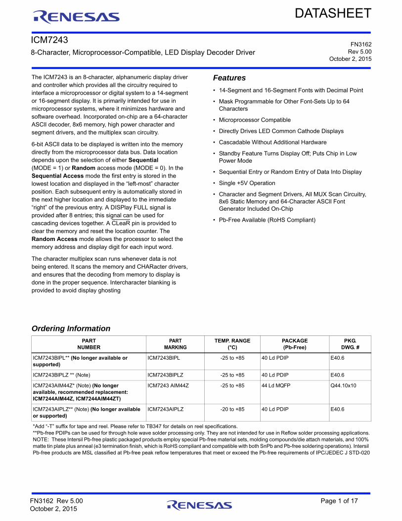
PinoutsICM7243A (16-SEGMENT CHARACTER)
(40 Ld PDIP)TOP VIEW
13
1
2
3
4
5
6
7
8
9
10
11
12
14
15
16
17
18
19
20
VDD
SEG m
SEG e
SEG g1
SEG k
SEG c
SEG d1
SEG a1
SEG a2
D0
D1
D2
D3
D4
D5
CS
WR
CHAR 8
CHAR 7
CHAR 6
28
40
39
38
37
36
35
34
33
32
31
30
29
27
26
25
24
23
22
21
SEG l
SEG g2
SEG b
SEG i
SEG f
SEG d2
D.P.
SEG h
SEG j
MODE
A0/SEN
A1/CLR
A2/DISP FULL
OSC/OFF
CHAR 1
CHAR 2
CHAR 3
CHAR 4
VSS
CHAR 5
FN3162 Rev 5.00 Page 2 of 17October 2, 2015
ICM7243
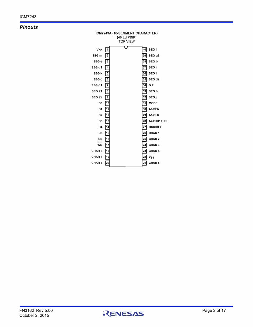
ICM7243B (14-SEGMENT CHARACTER) (40 Ld PDIP)TOP VIEW
ICM7243A (16-SEGMENT CHARACTER)(44 Ld MQFP)
TOP VIEW
Pinouts (Continued)
13
1
2
3
4
5
6
7
8
9
10
11
12
14
15
16
17
18
19
20
VDD
SEG e
SEG g1
SEG k
SEG c
SEG d
SEG a
D0
D1
D2
D3
D4
D5
CS
CS
CS
WR
CHAR 8
CHAR 7
CHAR 6
28
40
39
38
37
36
35
34
33
32
31
30
29
27
26
25
24
23
22
21
SEG m
SEG l
SEG g2
SEG b
SEG i
SEG f
D.P.
SEG h
SEG j
MODE
A0/SEN
A1/CLR
A2/DISP FULL
OSC/OFF
CHAR 1
CHAR 2
CHAR 3
CHAR 4
VSS
CHAR 5
D2
D1
D0
SEG a2
SEG a1
SEG d1 1
2
3
4
5
6
7
8
9
10
1112 13 14 15 16 17
D3
D4
D5
CS
NC
NC
WR
28
27
26
25
24
232221201918
VS
S
NC
NC
CHAR1
OSC/OFF
A2/DISP FULL
A1/CLR
A0/SEN
39 38 37 36 35 3433
32
31
30
29
44 43 42 41 40
VD
D
SE
G l
SE
G g
2
SE
G b
SE
G i
SE
G f
SEG d2
DP
SEG h
SEG j
MODE
SE
G c
SE
G k
SE
G g
1
SE
G e
SE
G m
CH
AR
8
CH
AR
7
CH
AR
6
CH
AR
5
CH
AR
4
CH
AR
3
CH
AR
2
NO LONGER AVAILABLE O
R SUPPORTED
FN3162 Rev 5.00 Page 3 of 17October 2, 2015
ICM7243
Functional Block Diagram
MODE
A0/SEN
A1/CLR
MULTIPLEXERSEQUENTIAL
CHARACTER
OSCILLATOR
DATA INPUTD0 - D5 D
Q
CL
DATALATCHES
8 x 6D1
CLCLR
D0
ADR
6 64 x 17ROM
SEGMENTDRIVERS
SEGMENT
ONESHOT
8
17
WRCSCSCS
MUX
SEL
D
CL
CLD ADDRESS
LATCHES
D CLQCONTROL
CL EN
CLR
SEQUENTIALADDRESSCOUNTER
OVERFLOW
LATCH
OUTPUTSSEG x
DATAMEMORY
8 8CHARACTER
DRIVERS
SEL3
ADDRESSMULITPLEXER
ANDDECODER
INTER-CHARACTER BLANKING
CHARACTERMULTIPLEXCOUNTER
MULTIPLEXOSCILLATOROSC/OFF
3
3
A2/DISP FULL
CHAR NCHARACTEROUTPUTS
(Note)
(NOTE 1)
NOTE: ICM7243A has only one CS and no CS.ICM7243B has 15 Segments.
(Note)
FN3162 Rev 5.00 Page 4 of 17October 2, 2015
ICM7243
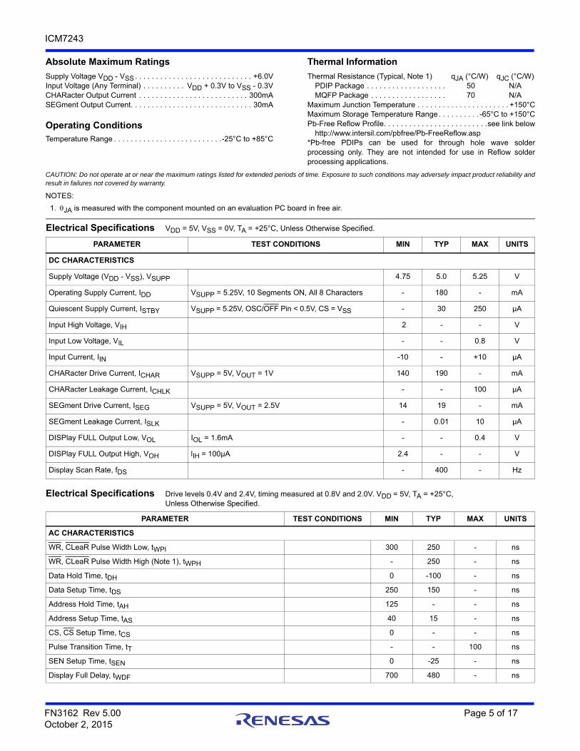
Absolute Maximum Ratings Thermal Information
Supply Voltage VDD - VSS . . . . . . . . . . . . . . . . . . . . . . . . . . . . +6.0VInput Voltage (Any Terminal) . . . . . . . . . . VDD + 0.3V to VSS - 0.3VCHARacter Output Current . . . . . . . . . . . . . . . . . . . . . . . . . . 300mASEGment Output Current. . . . . . . . . . . . . . . . . . . . . . . . . . . . . 30mA
Operating ConditionsTemperature Range . . . . . . . . . . . . . . . . . . . . . . . . . .-25°C to +85°C
Thermal Resistance (Typical, Note 1) qJA (°C/W) qJC (°C/W)PDIP Package . . . . . . . . . . . . . . . . . . . 50 N/AMQFP Package . . . . . . . . . . . . . . . . . . 70 N/A
Maximum Junction Temperature . . . . . . . . . . . . . . . . . . . . . . +150°CMaximum Storage Temperature Range . . . . . . . . . . -65°C to +150°CPb-Free Reflow Profile. . . . . . . . . . . . . . . . . . . . . . . . .see link below
http://www.intersil.com/pbfree/Pb-FreeReflow.asp*Pb-free PDIPs can be used for through hole wave solderprocessing only. They are not intended for use in Reflow solderprocessing applications.
CAUTION: Do not operate at or near the maximum ratings listed for extended periods of time. Exposure to such conditions may adversely impact product reliability andresult in failures not covered by warranty.
NOTES:
1. JA is measured with the component mounted on an evaluation PC board in free air.
Electrical Specifications VDD = 5V, VSS = 0V, TA = +25°C, Unless Otherwise Specified.
PARAMETER TEST CONDITIONS MIN TYP MAX UNITS
DC CHARACTERISTICS
Supply Voltage (VDD - VSS), VSUPP 4.75 5.0 5.25 V
Operating Supply Current, IDD VSUPP = 5.25V, 10 Segments ON, All 8 Characters - 180 - mA
Quiescent Supply Current, ISTBY VSUPP = 5.25V, OSC/OFF Pin < 0.5V, CS = VSS - 30 250 µA
Input High Voltage, VIH 2 - - V
Input Low Voltage, VIL - - 0.8 V
Input Current, IIN -10 - +10 µA
CHARacter Drive Current, ICHAR VSUPP = 5V, VOUT = 1V 140 190 - mA
CHARacter Leakage Current, ICHLK - - 100 µA
SEGment Drive Current, ISEG VSUPP = 5V, VOUT = 2.5V 14 19 - mA
SEGment Leakage Current, ISLK - 0.01 10 µA
DISPlay FULL Output Low, VOL IOL = 1.6mA - - 0.4 V
DISPlay FULL Output High, VOH lIH = 100µA 2.4 - - V
Display Scan Rate, fDS - 400 - Hz
Electrical Specifications Drive levels 0.4V and 2.4V, timing measured at 0.8V and 2.0V. VDD = 5V, TA = +25°C,
Unless Otherwise Specified.
PARAMETER TEST CONDITIONS MIN TYP MAX UNITS
AC CHARACTERISTICS
WR, CLeaR Pulse Width Low, tWPI 300 250 - ns
WR, CLeaR Pulse Width High (Note 1), tWPH - 250 - ns
Data Hold Time, tDH 0 -100 - ns
Data Setup Time, tDS 250 150 - ns
Address Hold Time, tAH 125 - - ns
Address Setup Time, tAS 40 15 - ns
CS, CS Setup Time, tCS 0 - - ns
Pulse Transition Time, tT - - 100 ns
SEN Setup Time, tSEN 0 -25 - ns
Display Full Delay, tWDF 700 480 - ns
FN3162 Rev 5.00 Page 5 of 17October 2, 2015
ICM7243
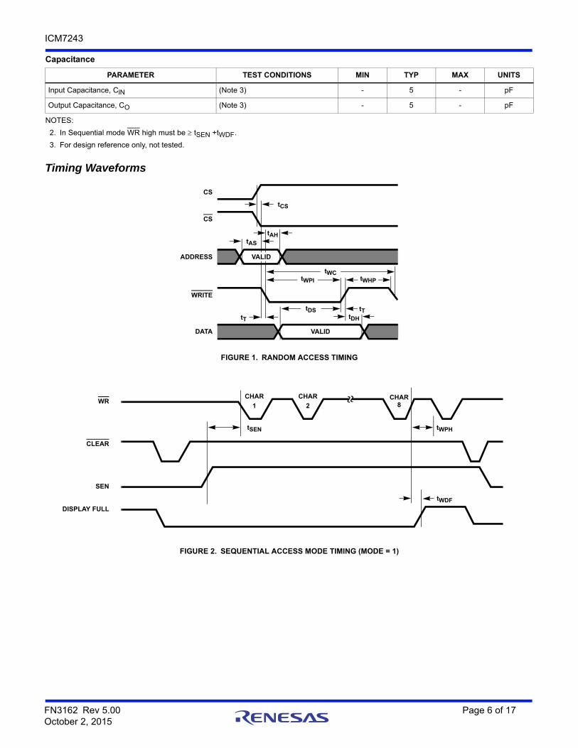
Capacitance
PARAMETER TEST CONDITIONS MIN TYP MAX UNITS
Input Capacitance, ClN (Note 3) - 5 - pF
Output Capacitance, CO (Note 3) - 5 - pF
NOTES:
2. In Sequential mode WR high must be tSEN +tWDF.
3. For design reference only, not tested.
Timing Waveforms
FIGURE 1. RANDOM ACCESS TIMING
FIGURE 2. SEQUENTIAL ACCESS MODE TIMING (MODE = 1)
CS
CS
ADDRESS
WRITE
DATA VALID
tCS
tAHtAS
tT tDH
tT
tWCtWPI tWHP
tDS
VALID
tWPH
WR
CLEAR
SEN
DISPLAY FULL
CHAR
tSEN
CHAR CHAR
tWDF
1 2 8
FN3162 Rev 5.00 Page 6 of 17October 2, 2015
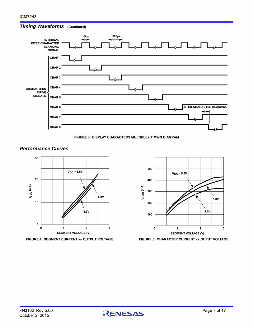
ICM7243
FIGURE 3. DISPLAY CHARACTERS MULTIPLEX TIMING DIAGRAM
Performance Curves
FIGURE 4. SEGMENT CURRENT vs OUTPUT VOLTAGE FIGURE 5. CHARACTER CURRENT vs OUPUT VOLTAGE
Timing Waveforms (Continued)
INTERNAL
CHAR 1
CHARACTERSDRIVE
SIGNALS
~5µs ~300µs
INTER-CHARACTER BLANKING
CHAR 2
CHAR 3
CHAR 4
CHAR 5
CHAR 6
CHAR 7
CHAR 8
INTER-CHARACTERBLANKING
SIGNAL
30
20
10
0 1 2 3
I SE
G (
mA
)
SEGMENT VOLTAGE (V)
VDD = 5.5V
4.5V
0
5.0V
I CH
AR
(m
A)
VDD = 5.5V
4.5V
5.0V
0 1 2 3
SEGMENT VOLTAGE (V)
100
200
300
400
500
FN3162 Rev 5.00 Page 7 of 17October 2, 2015
ICM7243
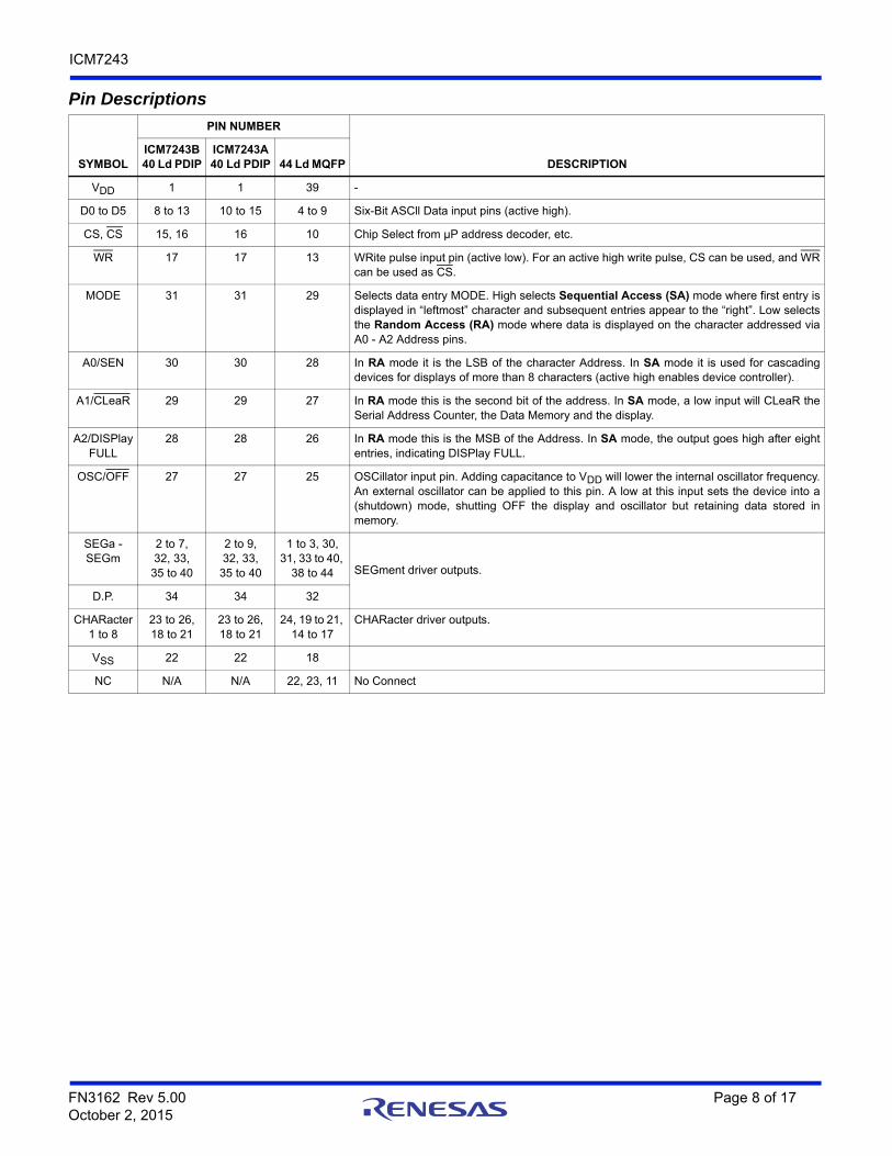
Pin Descriptions
SYMBOL
PIN NUMBER
DESCRIPTIONICM7243B40 Ld PDIP
ICM7243A40 Ld PDIP 44 Ld MQFP
VDD 1 1 39 -
D0 to D5 8 to 13 10 to 15 4 to 9 Six-Bit ASCll Data input pins (active high).
CS, CS 15, 16 16 10 Chip Select from µP address decoder, etc.
WR 17 17 13 WRite pulse input pin (active low). For an active high write pulse, CS can be used, and WRcan be used as CS.
MODE 31 31 29 Selects data entry MODE. High selects Sequential Access (SA) mode where first entry isdisplayed in “leftmost” character and subsequent entries appear to the “right”. Low selectsthe Random Access (RA) mode where data is displayed on the character addressed viaA0 - A2 Address pins.
A0/SEN 30 30 28 In RA mode it is the LSB of the character Address. In SA mode it is used for cascadingdevices for displays of more than 8 characters (active high enables device controller).
A1/CLeaR 29 29 27 In RA mode this is the second bit of the address. In SA mode, a low input will CLeaR theSerial Address Counter, the Data Memory and the display.
A2/DISPlay FULL
28 28 26 In RA mode this is the MSB of the Address. In SA mode, the output goes high after eightentries, indicating DISPlay FULL.
OSC/OFF 27 27 25 OSCillator input pin. Adding capacitance to VDD will lower the internal oscillator frequency.An external oscillator can be applied to this pin. A low at this input sets the device into a(shutdown) mode, shutting OFF the display and oscillator but retaining data stored inmemory.
SEGa -SEGm
2 to 7,32, 33,
35 to 40
2 to 9,32, 33,
35 to 40
1 to 3, 30, 31, 33 to 40,
38 to 44 SEGment driver outputs.
D.P. 34 34 32
CHARacter 1 to 8
23 to 26, 18 to 21
23 to 26, 18 to 21
24, 19 to 21, 14 to 17
CHARacter driver outputs.
VSS 22 22 18
NC N/A N/A 22, 23, 11 No Connect
FN3162 Rev 5.00 Page 8 of 17October 2, 2015
ICM7243
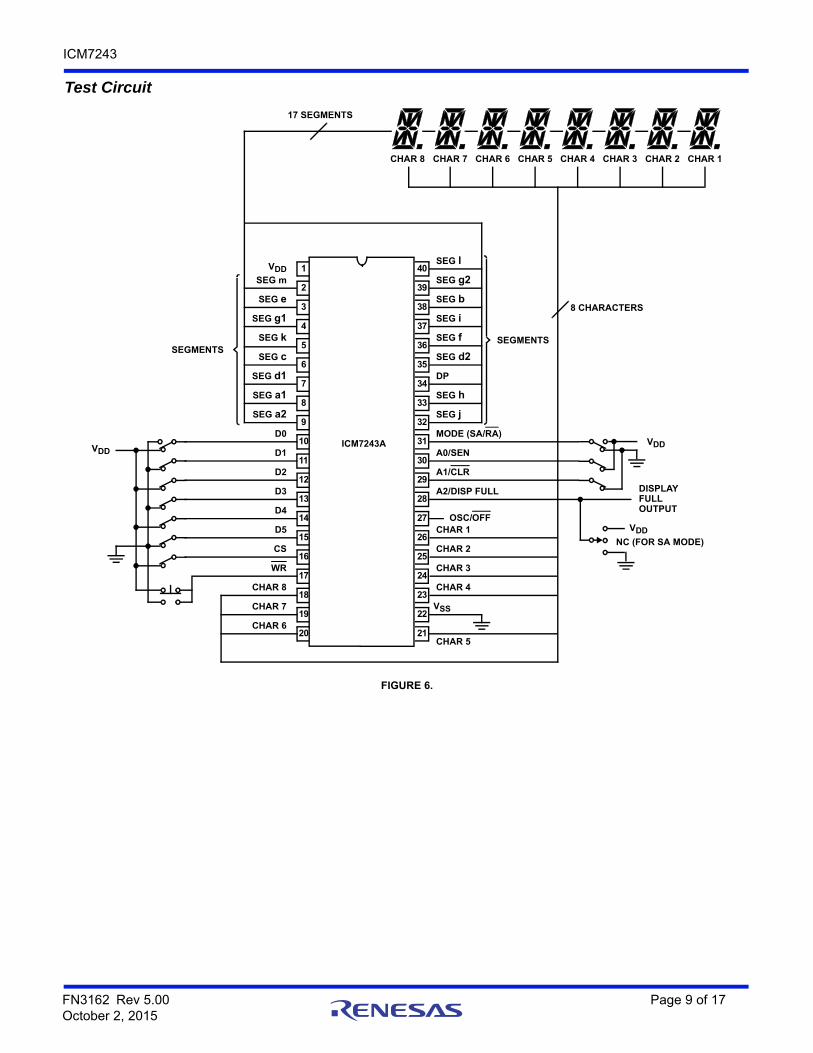
Test Circuit
FIGURE 6.
13
1
2
3
4
5
6
7
8
9
10
11
12
14
15
16
17
18
19
20
VDDSEG m
SEG e
SEG g1
SEG k
SEG c
SEG d1
SEG a1
SEG a2
D0
D1
D2
D3
D4
D5
CS
WR
CHAR 8
CHAR 7
CHAR 6
28
40
39
38
37
36
35
34
33
32
31
30
29
27
26
25
24
23
22
21
SEG l
SEG g2
SEG b
SEG i
SEG f
SEG d2
DP
SEG h
SEG j
MODE (SA/RA)
A0/SEN
A1/CLR
A2/DISP FULL
OSC/OFFCHAR 1
CHAR 2
CHAR 3
CHAR 4
CHAR 5
17 SEGMENTS
CHAR 8
SEGMENTS
8 CHARACTERS
VDD
DISPLAY
VDD
NC (FOR SA MODE)
CHAR 7 CHAR 6 CHAR 5 CHAR 4 CHAR 3 CHAR 2 CHAR 1
SEGMENTS
VDD
FULLOUTPUT
ICM7243A
VSS
FN3162 Rev 5.00 Page 9 of 17October 2, 2015
ICM7243
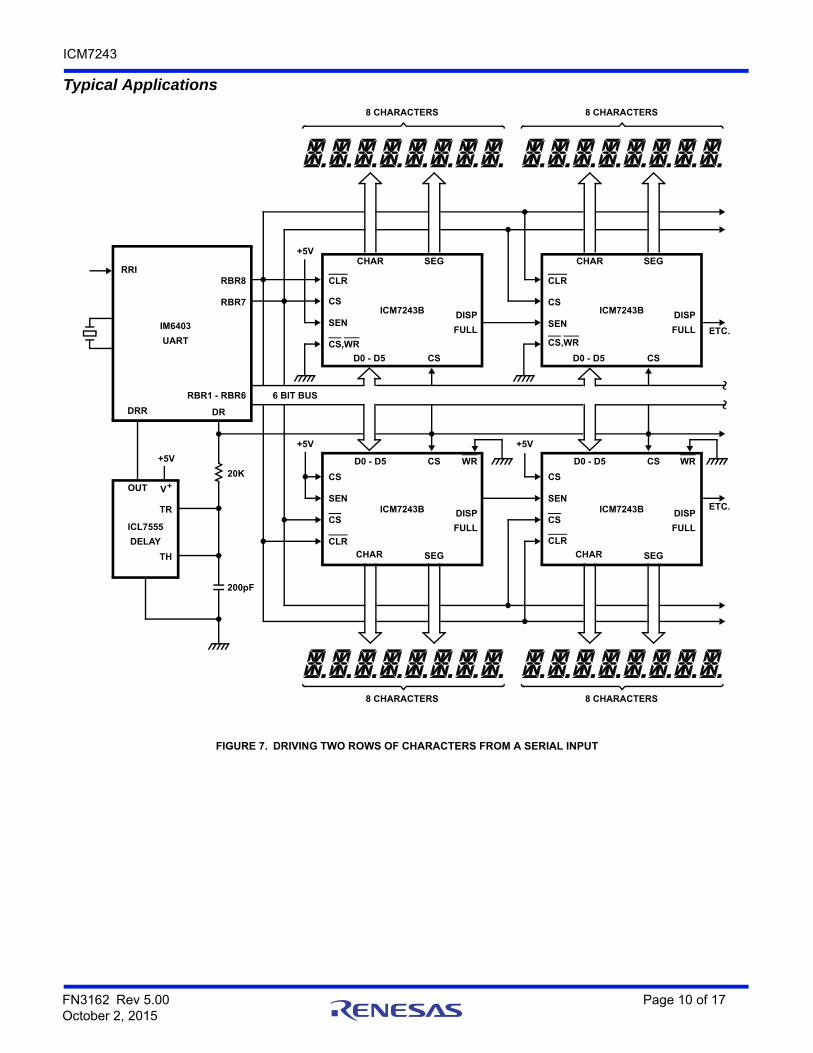
Typical Applications
FIGURE 7. DRIVING TWO ROWS OF CHARACTERS FROM A SERIAL INPUT
RRI
DRR
IM6403
UART
RBR1 - RBR6
RBR8
RBR7
DR
6 BIT BUS
+5V
CLR
CS
SEN
CS,WR
D0 - D5 CS
ICM7243B
SEG
DISP
FULL
CHAR
ETC.
ETC.
CLR
CS
SEN
CS,WR
D0 - D5 CS
ICM7243B
SEG
DISP
FULL
CHAR
CS
SEN
CS
CLR
CHAR SEG
ICM7243B
CS
DISP
FULL
D0 - D5
CS
SEN
CS
CLR
CHAR SEG
ICM7243B
CS
DISP
FULL
D0 - D5 WRWR
200pF
OUT V+
TR
TH
ICL7555
DELAY
20K
+5V +5V
+5V
8 CHARACTERS 8 CHARACTERS
8 CHARACTERS 8 CHARACTERS
FN3162 Rev 5.00 Page 10 of 17October 2, 2015
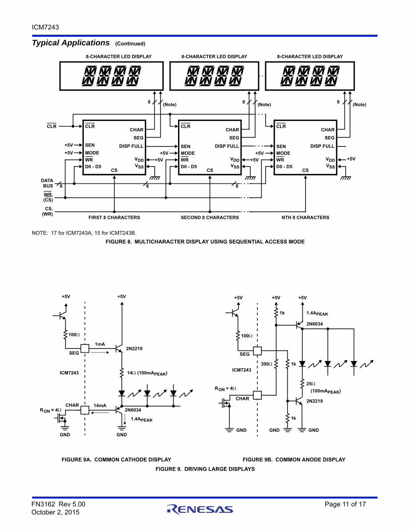
ICM7243
NOTE: 17 for ICM7243A, 15 for ICM7243B.
FIGURE 8. MULTICHARACTER DISPLAY USING SEQUENTIAL ACCESS MODE
FIGURE 9A. COMMON CATHODE DISPLAY FIGURE 9B. COMMON ANODE DISPLAY
FIGURE 9. DRIVING LARGE DISPLAYS
Typical Applications (Continued)
8-CHARACTER LED DISPLAY
8
CLR
+5V SEN
MODE
WR
D0 - D5CS
CHAR
SEG
DISP FULL
VDDVSS
DATA
WR,
CS,
FIRST 8 CHARACTERS SECOND 8 CHARACTERS NTH 8 CHARACTERS
8-CHARACTER LED DISPLAY 8-CHARACTER LED DISPLAY
8 8
+5V
CLR CLR
SEN
MODE
WR
D0 - D5CS
CHAR
SEG
DISP FULL
VDDVSS
CLR
SEN
MODE
WR
D0 - D5CS
CHAR
SEG
DISP FULL
VDDVSS
+5V
+5V
+5V
+5V +5V
6
(Note)
6
(Note) (Note)
6
(CS)
BUS
(WR)
+5V
100
1mA2N2219
14 (100mAPEAK)
CHAR 14mA2N6034
1.4APEAK
GND
RON = 4
ICM7243
+5V
GND
SEG
+5V
100
2N2219
(100mAPEAK)
1.4APEAK
GND
RON = 4
ICM7243
+5V
GND
SEG
300
GND
+5V
1k
1k
25
1k
CHAR
2N6034
FN3162 Rev 5.00 Page 11 of 17October 2, 2015
ICM7243
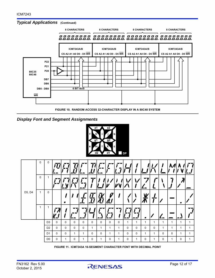
FIGURE 10. RANDOM ACCESS 32-CHARACTER DISPLAY IN A 80C48 SYSTEM
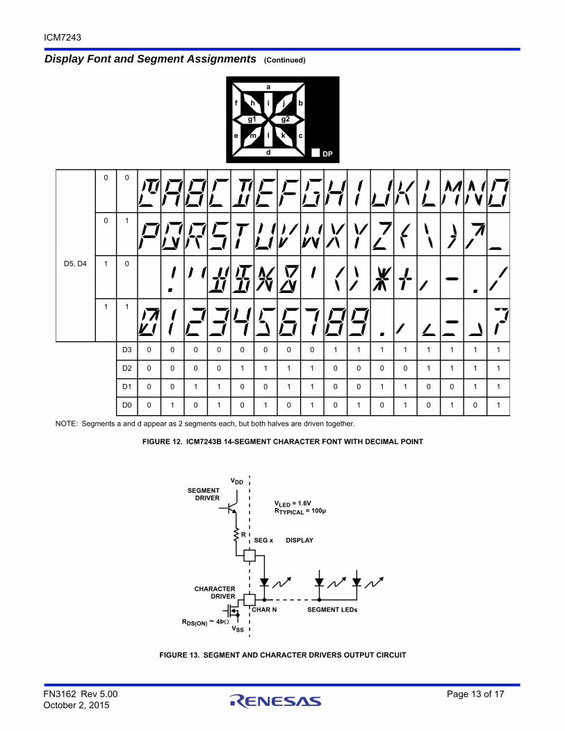
Display Font and Segment Assignments
FIGURE 11. ICM7243A 16-SEGMENT CHARACTER FONT WITH DECIMAL POINT
Typical Applications (Continued)
CS A2 A1 A0 D0 - D5 WR CS A2 A1 A0 D0 - D5 WR CS A2 A1 A0 D0 - D5 WRCS A2 A1 A0 D0 - D5 WR
80C3580C48
WR
DB5 - DB0
DB6
DB7
P22
P21
P20
6 BIT BUS
ICM7243A/B ICM7243A/B ICM7243A/B ICM7243A/B
8 CHARACTERS 8 CHARACTERS 8 CHARACTERS 8 CHARACTERS
0 0
0 1
D5, D4 1 0
1 1
D3 0 0 0 0 0 0 0 0 1 1 1 1 1 1 1 1
D2 0 0 0 0 1 1 1 1 0 0 0 0 1 1 1 1
D1 0 0 1 1 0 0 1 1 0 0 1 1 0 0 1 1
D0 0 1 0 1 0 1 0 1 0 1 0 1 0 1 0 1
g1 g2
km l
f
e
b
c
a1
h ji
a2
d2 d1 DP
FN3162 Rev 5.00 Page 12 of 17October 2, 2015
ICM7243
FIGURE 12. ICM7243B 14-SEGMENT CHARACTER FONT WITH DECIMAL POINT
FIGURE 13. SEGMENT AND CHARACTER DRIVERS OUTPUT CIRCUIT
Display Font and Segment Assignments (Continued)
0 0
0 1
D5, D4 1 0
1 1
D3 0 0 0 0 0 0 0 0 1 1 1 1 1 1 1 1
D2 0 0 0 0 1 1 1 1 0 0 0 0 1 1 1 1
D1 0 0 1 1 0 0 1 1 0 0 1 1 0 0 1 1
D0 0 1 0 1 0 1 0 1 0 1 0 1 0 1 0 1
NOTE: Segments a and d appear as 2 segments each, but both halves are driven together.
g1 g2
km l
f
e
b
c
a1
h ji
a2
d2 d1
g1 g2
km
f
e
b
c
h ji
a
d1 DP
l
d
VDD
SEGMENTDRIVER
R
CHARACTERDRIVER
RDS(ON) ~ 4ÞVSS
CHAR N SEGMENT LEDs
SEG x DISPLAY
VLED = 1.6VRTYPICAL = 100µ
FN3162 Rev 5.00 Page 13 of 17October 2, 2015
ICM7243
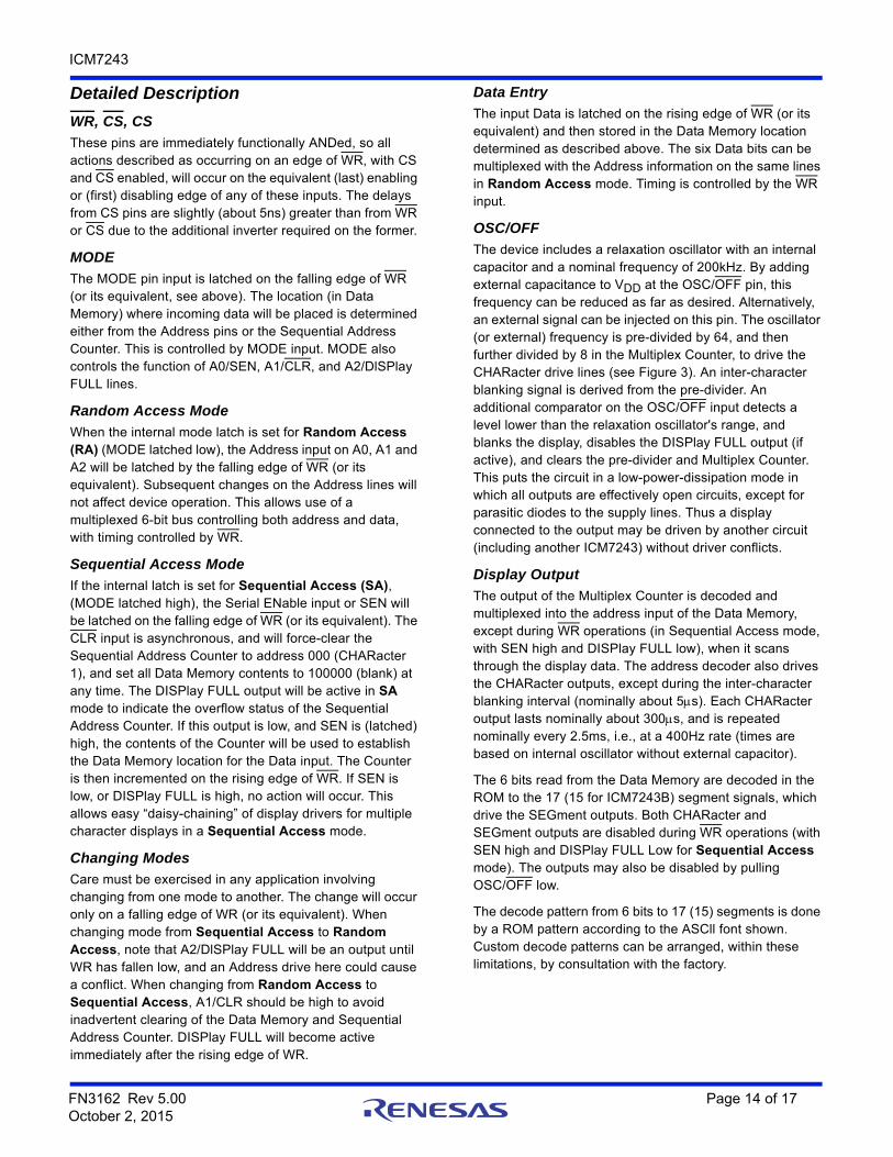
Detailed Description
WR, CS, CS
These pins are immediately functionally ANDed, so all actions described as occurring on an edge of WR, with CS and CS enabled, will occur on the equivalent (last) enabling or (first) disabling edge of any of these inputs. The delays from CS pins are slightly (about 5ns) greater than from WR or CS due to the additional inverter required on the former.
MODE
The MODE pin input is latched on the falling edge of WR (or its equivalent, see above). The location (in Data Memory) where incoming data will be placed is determined either from the Address pins or the Sequential Address Counter. This is controlled by MODE input. MODE also controls the function of A0/SEN, A1/CLR, and A2/DlSPlay FULL lines.
Random Access Mode
When the internal mode latch is set for Random Access (RA) (MODE latched low), the Address input on A0, A1 and A2 will be latched by the falling edge of WR (or its equivalent). Subsequent changes on the Address lines will not affect device operation. This allows use of a multiplexed 6-bit bus controlling both address and data, with timing controlled by WR.
Sequential Access Mode
If the internal latch is set for Sequential Access (SA), (MODE latched high), the Serial ENable input or SEN will be latched on the falling edge of WR (or its equivalent). The CLR input is asynchronous, and will force-clear the Sequential Address Counter to address 000 (CHARacter 1), and set all Data Memory contents to 100000 (blank) at any time. The DISPlay FULL output will be active in SA mode to indicate the overflow status of the Sequential Address Counter. If this output is low, and SEN is (latched) high, the contents of the Counter will be used to establish the Data Memory location for the Data input. The Counter is then incremented on the rising edge of WR. If SEN is low, or DISPlay FULL is high, no action will occur. This allows easy “daisy-chaining” of display drivers for multiple character displays in a Sequential Access mode.
Changing Modes
Care must be exercised in any application involving changing from one mode to another. The change will occur only on a falling edge of WR (or its equivalent). When changing mode from Sequential Access to Random Access, note that A2/DlSPlay FULL will be an output until WR has fallen low, and an Address drive here could cause a conflict. When changing from Random Access to Sequential Access, A1/CLR should be high to avoid inadvertent clearing of the Data Memory and Sequential Address Counter. DISPlay FULL will become active immediately after the rising edge of WR.
Data Entry
The input Data is latched on the rising edge of WR (or its equivalent) and then stored in the Data Memory location determined as described above. The six Data bits can be multiplexed with the Address information on the same lines in Random Access mode. Timing is controlled by the WR input.
OSC/OFF
The device includes a relaxation oscillator with an internal capacitor and a nominal frequency of 200kHz. By adding external capacitance to VDD at the OSC/OFF pin, this frequency can be reduced as far as desired. Alternatively, an external signal can be injected on this pin. The oscillator (or external) frequency is pre-divided by 64, and then further divided by 8 in the Multiplex Counter, to drive the CHARacter drive lines (see Figure 3). An inter-character blanking signal is derived from the pre-divider. An additional comparator on the OSC/OFF input detects a level lower than the relaxation oscillator's range, and blanks the display, disables the DISPlay FULL output (if active), and clears the pre-divider and Multiplex Counter. This puts the circuit in a low-power-dissipation mode in which all outputs are effectively open circuits, except for parasitic diodes to the supply lines. Thus a display connected to the output may be driven by another circuit (including another ICM7243) without driver conflicts.
Display Output
The output of the Multiplex Counter is decoded and multiplexed into the address input of the Data Memory, except during WR operations (in Sequential Access mode, with SEN high and DISPlay FULL low), when it scans through the display data. The address decoder also drives the CHARacter outputs, except during the inter-character blanking interval (nominally about 5s). Each CHARacter output lasts nominally about 300s, and is repeated nominally every 2.5ms, i.e., at a 400Hz rate (times are based on internal oscillator without external capacitor).
The 6 bits read from the Data Memory are decoded in the ROM to the 17 (15 for ICM7243B) segment signals, which drive the SEGment outputs. Both CHARacter and SEGment outputs are disabled during WR operations (with SEN high and DISPlay FULL Low for Sequential Access mode). The outputs may also be disabled by pulling OSC/OFF low.
The decode pattern from 6 bits to 17 (15) segments is done by a ROM pattern according to the ASCll font shown. Custom decode patterns can be arranged, within these limitations, by consultation with the factory.
FN3162 Rev 5.00 Page 14 of 17October 2, 2015
ICM7243
About IntersilIntersil Corporation is a leading provider of innovative power management and precision analog solutions. The company's products address some of the largest markets within the industrial and infrastructure, mobile computing and high-end consumer markets.
For the most updated datasheet, application notes, related documentation and related parts, please see the respective product information page found at www.intersil.com.
You may report errors or suggestions for improving this datasheet by visiting www.intersil.com/ask.
Reliability reports are also available from our website at www.intersil.com/support
Revision HistoryThe revision history provided is for informational purposes only and is believed to be accurate, but not warranted. Please go to the web to make sure that you have the latest revision.
DATE REVISION CHANGE
October 2, 2015 FN3162.5 Updated Ordering Information Table on page 1.Added Revision History and About Intersil sections.
FN3162 Rev 5.00 Page 15 of 17October 2, 2015
ICM7243
FN3162 Rev 5.00 Page 16 of 17October 2, 2015
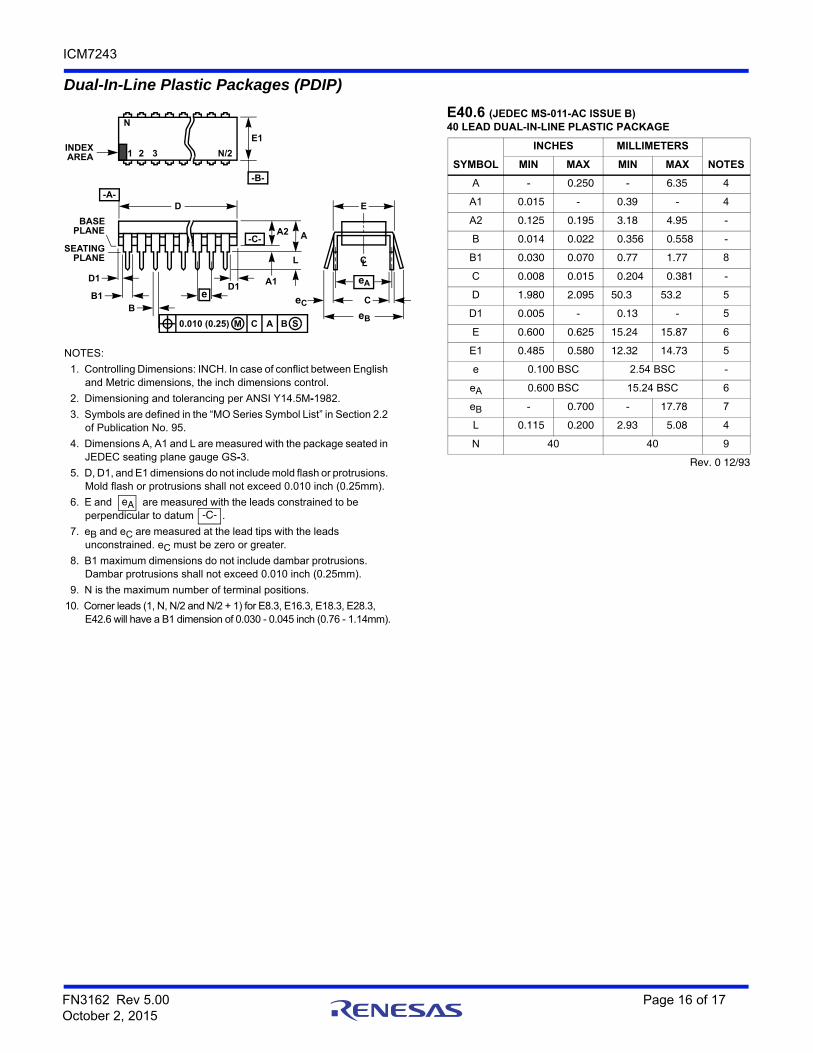
Dual-In-Line Plastic Packages (PDIP)
NOTES:
1. Controlling Dimensions: INCH. In case of conflict between English and Metric dimensions, the inch dimensions control.
2. Dimensioning and tolerancing per ANSI Y14.5M-1982.
3. Symbols are defined in the “MO Series Symbol List” in Section 2.2 of Publication No. 95.
4. Dimensions A, A1 and L are measured with the package seated in JEDEC seating plane gauge GS-3.
5. D, D1, and E1 dimensions do not include mold flash or protrusions. Mold flash or protrusions shall not exceed 0.010 inch (0.25mm).
6. E and are measured with the leads constrained to be perpendicular to datum .
7. eB and eC are measured at the lead tips with the leads unconstrained. eC must be zero or greater.
8. B1 maximum dimensions do not include dambar protrusions. Dambar protrusions shall not exceed 0.010 inch (0.25mm).
9. N is the maximum number of terminal positions.
10. Corner leads (1, N, N/2 and N/2 + 1) for E8.3, E16.3, E18.3, E28.3, E42.6 will have a B1 dimension of 0.030 - 0.045 inch (0.76 - 1.14mm).
eA-C-
CL
E
eA
C
eB
eC
-B-
E1INDEX
1 2 3 N/2
N
AREA
SEATING
BASEPLANE
PLANE
-C-
D1
B1B
e
D
D1
AA2
L
A1
-A-
0.010 (0.25) C AM B S
E40.6 (JEDEC MS-011-AC ISSUE B)40 LEAD DUAL-IN-LINE PLASTIC PACKAGE
SYMBOL
INCHES MILLIMETERS
NOTESMIN MAX MIN MAX
A - 0.250 - 6.35 4
A1 0.015 - 0.39 - 4
A2 0.125 0.195 3.18 4.95 -
B 0.014 0.022 0.356 0.558 -
B1 0.030 0.070 0.77 1.77 8
C 0.008 0.015 0.204 0.381 -
D 1.980 2.095 50.3 53.2 5
D1 0.005 - 0.13 - 5
E 0.600 0.625 15.24 15.87 6
E1 0.485 0.580 12.32 14.73 5
e 0.100 BSC 2.54 BSC -
eA 0.600 BSC 15.24 BSC 6
eB - 0.700 - 17.78 7
L 0.115 0.200 2.93 5.08 4
N 40 40 9
Rev. 0 12/93
FN3162 Rev 5.00 Page 17 of 17October 2, 2015
ICM7243
Intersil products are manufactured, assembled and tested utilizing ISO9001 quality systems as notedin the quality certifications found at www.intersil.com/en/support/qualandreliability.html
Intersil products are sold by description only. Intersil may modify the circuit design and/or specifications of products at any time without notice, provided that such modification does not, in Intersil's sole judgment, affect the form, fit or function of the product. Accordingly, the reader is cautioned to verify that datasheets are current before placing orders. Information furnished by Intersil is believed to be accurate and reliable. However, no responsibility is assumed by Intersil or its subsidiaries for its use; nor for any infringements of patents or other rights of third parties which may result from its use. No license is granted by implication or otherwise under any patent or patent rights of Intersil or its subsidiaries.
For information regarding Intersil Corporation and its products, see www.intersil.com
For additional products, see www.intersil.com/en/products.html
© Copyright Intersil Americas LLC 2003-2015. All Rights Reserved.All trademarks and registered trademarks are the property of their respective owners.
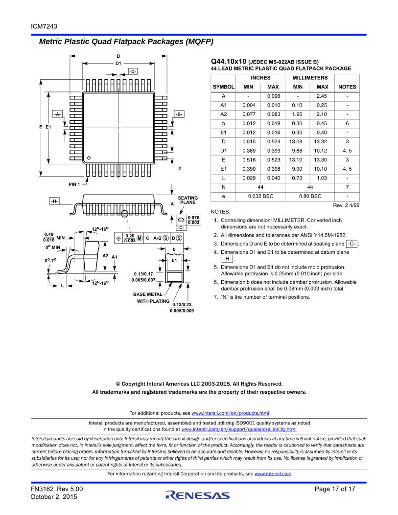
Metric Plastic Quad Flatpack Packages (MQFP)
D
D1
E E1
-A-
PIN 1
A2 A1
A
12o-16o
12o-16o
0o-7o
0.400.016 MIN
L
0o MIN
PLANE
b
0.005/0.0090.13/0.23
WITH PLATING
BASE METAL
SEATING
0.005/0.0070.13/0.17
b1
-B-
e
0.0080.20 A-B SD SCM
0.0760.003
-C-
-D-
-H-
Q44.10x10 (JEDEC MS-022AB ISSUE B)44 LEAD METRIC PLASTIC QUAD FLATPACK PACKAGE
SYMBOL
INCHES MILLIMETERS
NOTESMIN MAX MIN MAX
A - 0.096 - 2.45 -
A1 0.004 0.010 0.10 0.25 -
A2 0.077 0.083 1.95 2.10 -
b 0.012 0.018 0.30 0.45 6
b1 0.012 0.016 0.30 0.40 -
D 0.515 0.524 13.08 13.32 3
D1 0.389 0.399 9.88 10.12 4, 5
E 0.516 0.523 13.10 13.30 3
E1 0.390 0.398 9.90 10.10 4, 5
L 0.029 0.040 0.73 1.03 -
N 44 44 7
e 0.032 BSC 0.80 BSC -
Rev. 2 4/99NOTES:
1. Controlling dimension: MILLIMETER. Converted inch dimensions are not necessarily exact.
2. All dimensions and tolerances per ANSI Y14.5M-1982.
3. Dimensions D and E to be determined at seating plane .
4. Dimensions D1 and E1 to be determined at datum plane .
5. Dimensions D1 and E1 do not include mold protrusion. Allowable protrusion is 0.25mm (0.010 inch) per side.
6. Dimension b does not include dambar protrusion. Allowable dambar protrusion shall be 0.08mm (0.003 inch) total.
7. “N” is the number of terminal positions.
-C-
-H-