datasheet ci
DESCRIPTION
Datasheet circuito integrado, caracteristicas dadas por el fabricante para su correcto funcionamiento.TRANSCRIPT
Preliminary data
This is preliminary information on a new product now in development or undergoing evaluation. Details are subject to change without notice.
July 2011 Doc ID 022018 Rev 1 1/54
54
LSM330DLLinear sensor module
3D accelerometer sensor and 3D gyroscope sensor
Features Analog supply voltage 2.4 V to 3.6 V
Digital supply voltage I/Os, 1.8V
Low-power mode
Power-down mode
3 independent acceleration channels and 3 angular rate channels
±2g/±4g/±8g/±16g dynamic, selectable full-scale acceleration range
±250/±500/±2000 dps dynamic, selectable full-scale angular rate
SPI/I2C serial interface (16-bit data output)
Programmable interrupt generator for free-fall and motion detection
ECOPACK®, RoHS, and “Green” compliant
Applications GPS navigation systems
Impact recognition and logging
Gaming and virtual reality input devices
Motion-activated functions
Intelligent power saving for handheld devices
Vibration monitoring and compensation
Free-fall detection
6D-orientation detection
DescriptionThe LSM330DL is a system-in-package featuring a 3D digital accelerometer and a 3D digital gyroscope.
ST’s family of modules leverages a robust and mature manufacturing process already used for the production of micromachined accelerometers.
The various sensing elements are manufactured using specialized micromachining processes, while the IC interfaces are based on CMOS technology that allows designing a dedicated circuit which is trimmed to better match the sensing element characteristics.
The LSM330DL has a dynamic, user-selectable full-scale acceleration range of ±2g/±4g/±8g/±16g and an angular rate of ±250/±500/±2000 deg/sec.
The accelerometer and gyroscope sensors can be either activated or put in low-power / power-down mode separately for power-saving optimized applications. The LSM330DL is available in a plastic land grid array (LGA) package.
Several years ago ST successfully pioneered the use of this package for accelerometers. Today, ST has the broadest manufacturing capability in the world and unrivalled expertise for the production of sensors in a plastic LGA package.
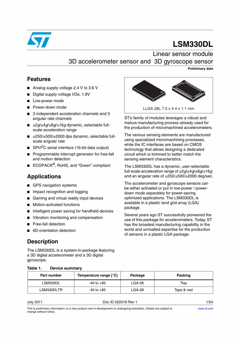
LLGA 28L 7.5 x 4.4 x 1.1 mm
Table 1. Device summary
Part number Temperature range [°C] Package Packing
LSM330DL -40 to +85 LGA-28 Tray
LSM330DLTR -40 to +85 LGA-28 Tape & reel
www.st.com
Contents LSM330DL
2/54 Doc ID 022018 Rev 1
Contents
1 Block diagram and pin description . . . . . . . . . . . . . . . . . . . . . . . . . . . . . 9
1.1 Block diagram . . . . . . . . . . . . . . . . . . . . . . . . . . . . . . . . . . . . . . . . . . . . . . . 9
1.2 Pin description . . . . . . . . . . . . . . . . . . . . . . . . . . . . . . . . . . . . . . . . . . . . . 10
2 Module specifications . . . . . . . . . . . . . . . . . . . . . . . . . . . . . . . . . . . . . . . 12
2.1 Mechanical characteristics . . . . . . . . . . . . . . . . . . . . . . . . . . . . . . . . . . . . 12
2.2 Electrical characteristics . . . . . . . . . . . . . . . . . . . . . . . . . . . . . . . . . . . . . . 13
2.3 Temperature sensor characteristics . . . . . . . . . . . . . . . . . . . . . . . . . . . . . 13
2.4 Communication interface characteristics . . . . . . . . . . . . . . . . . . . . . . . . . 14
2.4.1 SPI - serial peripheral interface . . . . . . . . . . . . . . . . . . . . . . . . . . . . . . . 14
2.4.2 I2C - inter-IC control interface . . . . . . . . . . . . . . . . . . . . . . . . . . . . . . . . 15
2.5 Absolute maximum ratings . . . . . . . . . . . . . . . . . . . . . . . . . . . . . . . . . . . . 16
2.6 Terminology . . . . . . . . . . . . . . . . . . . . . . . . . . . . . . . . . . . . . . . . . . . . . . . 17
2.6.1 Sensitivity . . . . . . . . . . . . . . . . . . . . . . . . . . . . . . . . . . . . . . . . . . . . . . . . 17
2.6.2 Zero level . . . . . . . . . . . . . . . . . . . . . . . . . . . . . . . . . . . . . . . . . . . . . . . . 17
3 Functionality . . . . . . . . . . . . . . . . . . . . . . . . . . . . . . . . . . . . . . . . . . . . . . 18
3.1 Factory calibration . . . . . . . . . . . . . . . . . . . . . . . . . . . . . . . . . . . . . . . . . . 18
4 Application hints . . . . . . . . . . . . . . . . . . . . . . . . . . . . . . . . . . . . . . . . . . . 19
4.1 External capacitors . . . . . . . . . . . . . . . . . . . . . . . . . . . . . . . . . . . . . . . . . . 19
4.2 Soldering information . . . . . . . . . . . . . . . . . . . . . . . . . . . . . . . . . . . . . . . . 20
5 Digital interfaces . . . . . . . . . . . . . . . . . . . . . . . . . . . . . . . . . . . . . . . . . . . 21
5.1 I2C serial interface . . . . . . . . . . . . . . . . . . . . . . . . . . . . . . . . . . . . . . . . . . 21
5.1.1 I2C operation . . . . . . . . . . . . . . . . . . . . . . . . . . . . . . . . . . . . . . . . . . . . . 22
5.2 SPI bus interface . . . . . . . . . . . . . . . . . . . . . . . . . . . . . . . . . . . . . . . . . . . 24
5.2.1 SPI read . . . . . . . . . . . . . . . . . . . . . . . . . . . . . . . . . . . . . . . . . . . . . . . . . 25
5.2.2 SPI write . . . . . . . . . . . . . . . . . . . . . . . . . . . . . . . . . . . . . . . . . . . . . . . . 25
5.2.3 SPI read in 3-wire mode . . . . . . . . . . . . . . . . . . . . . . . . . . . . . . . . . . . . 26
6 Register mapping . . . . . . . . . . . . . . . . . . . . . . . . . . . . . . . . . . . . . . . . . . 27
LSM330DL Contents
Doc ID 022018 Rev 1 3/54
7 Registers description . . . . . . . . . . . . . . . . . . . . . . . . . . . . . . . . . . . . . . . 29
7.1 CTRL_REG1_A (20h) . . . . . . . . . . . . . . . . . . . . . . . . . . . . . . . . . . . . . . . 29
7.2 CTRL_REG2_A (21h) . . . . . . . . . . . . . . . . . . . . . . . . . . . . . . . . . . . . . . . 30
7.3 CTRL_REG3_A (22h) . . . . . . . . . . . . . . . . . . . . . . . . . . . . . . . . . . . . . . . 31
7.4 CTRL_REG4_A (23h) . . . . . . . . . . . . . . . . . . . . . . . . . . . . . . . . . . . . . . . 31
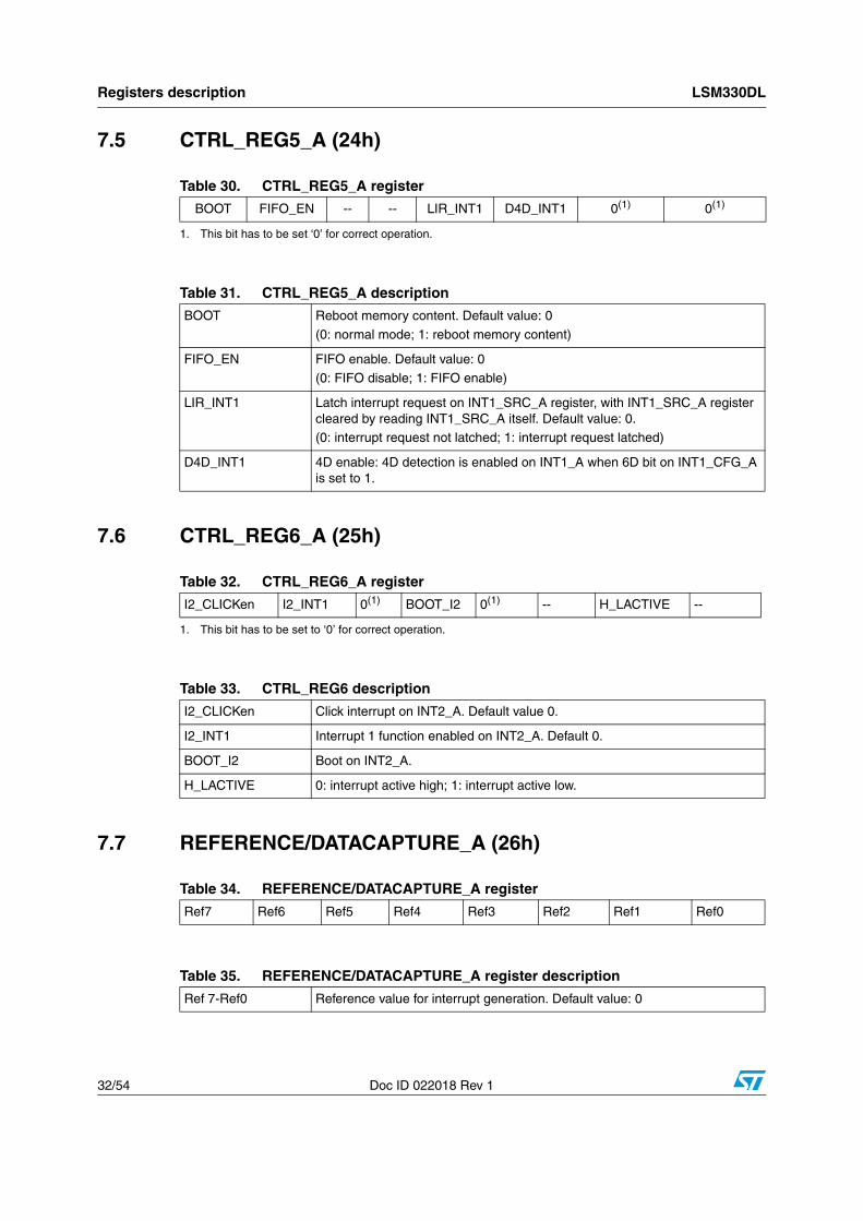
7.5 CTRL_REG5_A (24h) . . . . . . . . . . . . . . . . . . . . . . . . . . . . . . . . . . . . . . . 32
7.6 CTRL_REG6_A (25h) . . . . . . . . . . . . . . . . . . . . . . . . . . . . . . . . . . . . . . . 32
7.7 REFERENCE/DATACAPTURE_A (26h) . . . . . . . . . . . . . . . . . . . . . . . . . . 32
7.8 STATUS_REG_A (27h) . . . . . . . . . . . . . . . . . . . . . . . . . . . . . . . . . . . . . . 33
7.9 OUT_X_L_A (28h), OUT_X_H_A (29h) . . . . . . . . . . . . . . . . . . . . . . . . . . 33
7.10 OUT_Y_L_A (2Ah), OUT_Y_H_A (2Bh) . . . . . . . . . . . . . . . . . . . . . . . . . 33
7.11 OUT_Z_L _A(2Ch), OUT_Z_H_A (2Dh) . . . . . . . . . . . . . . . . . . . . . . . . . 33
7.12 FIFO_CTRL_REG_A (2Eh) . . . . . . . . . . . . . . . . . . . . . . . . . . . . . . . . . . . 33
7.13 FIFO_SRC_REG_A (2Fh) . . . . . . . . . . . . . . . . . . . . . . . . . . . . . . . . . . . . 34
7.14 INT1_CFG_A (30h) . . . . . . . . . . . . . . . . . . . . . . . . . . . . . . . . . . . . . . . . . 34
7.15 INT1_SRC_A (31h) . . . . . . . . . . . . . . . . . . . . . . . . . . . . . . . . . . . . . . . . . 35
7.16 INT1_THS_A (32h) . . . . . . . . . . . . . . . . . . . . . . . . . . . . . . . . . . . . . . . . . . 36
7.17 INT1_DURATION_A (33h) . . . . . . . . . . . . . . . . . . . . . . . . . . . . . . . . . . . . 36
7.18 CLICK_CFG _A (38h) . . . . . . . . . . . . . . . . . . . . . . . . . . . . . . . . . . . . . . . 36
7.19 CLICK_SRC_A (39h) . . . . . . . . . . . . . . . . . . . . . . . . . . . . . . . . . . . . . . . . 37
7.20 CLICK_THS_A (3Ah) . . . . . . . . . . . . . . . . . . . . . . . . . . . . . . . . . . . . . . . . 38
7.21 TIME_LIMIT_A (3Bh) . . . . . . . . . . . . . . . . . . . . . . . . . . . . . . . . . . . . . . . . 38
7.22 TIME_LATENCY_A (3Ch) . . . . . . . . . . . . . . . . . . . . . . . . . . . . . . . . . . . . 38
7.23 TIME WINDOW_A (3Dh) . . . . . . . . . . . . . . . . . . . . . . . . . . . . . . . . . . . . . 38
7.24 CTRL_REG1_G (20h) . . . . . . . . . . . . . . . . . . . . . . . . . . . . . . . . . . . . . . . 39
7.25 CTRL_REG2_G (21h) . . . . . . . . . . . . . . . . . . . . . . . . . . . . . . . . . . . . . . . 40
7.26 CTRL_REG3_G (22h) . . . . . . . . . . . . . . . . . . . . . . . . . . . . . . . . . . . . . . . 41
7.27 CTRL_REG4_G (23h) . . . . . . . . . . . . . . . . . . . . . . . . . . . . . . . . . . . . . . . 41
7.28 CTRL_REG5_G (24h) . . . . . . . . . . . . . . . . . . . . . . . . . . . . . . . . . . . . . . . 42
7.29 REFERENCE/DATACAPTURE_G (25h) . . . . . . . . . . . . . . . . . . . . . . . . . 43
7.30 OUT_TEMP_G (26h) . . . . . . . . . . . . . . . . . . . . . . . . . . . . . . . . . . . . . . . . 43
7.31 STATUS_REG_G (27h) . . . . . . . . . . . . . . . . . . . . . . . . . . . . . . . . . . . . . . 44
7.32 OUT_X_L_G (28h), OUT_X_H_G (29h) . . . . . . . . . . . . . . . . . . . . . . . . . 44
Contents LSM330DL
4/54 Doc ID 022018 Rev 1
7.33 OUT_Y_L_G (2Ah), OUT_Y_H_G (2Bh) . . . . . . . . . . . . . . . . . . . . . . . . . 44
7.34 OUT_Z_L_G (2Ch), OUT_Z_H_G (2Dh) . . . . . . . . . . . . . . . . . . . . . . . . . 44
7.35 FIFO_CTRL_REG_G (2Eh) . . . . . . . . . . . . . . . . . . . . . . . . . . . . . . . . . . . 45
7.36 FIFO_SRC_REG_G (2Fh) . . . . . . . . . . . . . . . . . . . . . . . . . . . . . . . . . . . . 45
7.37 INT1_CFG_G (30h) . . . . . . . . . . . . . . . . . . . . . . . . . . . . . . . . . . . . . . . . . 46
7.38 INT1_SRC_G (31h) . . . . . . . . . . . . . . . . . . . . . . . . . . . . . . . . . . . . . . . . . 47
7.39 INT1_THS_XH_G (32h) . . . . . . . . . . . . . . . . . . . . . . . . . . . . . . . . . . . . . . 47
7.40 INT1_THS_XL_G (33h) . . . . . . . . . . . . . . . . . . . . . . . . . . . . . . . . . . . . . . 47
7.41 INT1_THS_YH_G (34h) . . . . . . . . . . . . . . . . . . . . . . . . . . . . . . . . . . . . . . 48
7.42 INT1_THS_YL_G (35h) . . . . . . . . . . . . . . . . . . . . . . . . . . . . . . . . . . . . . . 48
7.43 INT1_THS_ZH_G (36h) . . . . . . . . . . . . . . . . . . . . . . . . . . . . . . . . . . . . . . 48
7.44 INT1_THS_ZL_G (37h) . . . . . . . . . . . . . . . . . . . . . . . . . . . . . . . . . . . . . . 48
7.45 INT1_DURATION_G (38h) . . . . . . . . . . . . . . . . . . . . . . . . . . . . . . . . . . . . 49
8 Package information . . . . . . . . . . . . . . . . . . . . . . . . . . . . . . . . . . . . . . . . 51
9 Revision history . . . . . . . . . . . . . . . . . . . . . . . . . . . . . . . . . . . . . . . . . . . 53
LSM330DL List of tables
Doc ID 022018 Rev 1 5/54
List of tables
Table 1. Device summary . . . . . . . . . . . . . . . . . . . . . . . . . . . . . . . . . . . . . . . . . . . . . . . . . . . . . . . . . . 1Table 2. Pin description . . . . . . . . . . . . . . . . . . . . . . . . . . . . . . . . . . . . . . . . . . . . . . . . . . . . . . . . . . 10Table 3. Mechanical characteristics . . . . . . . . . . . . . . . . . . . . . . . . . . . . . . . . . . . . . . . . . . . . . . . . . 12Table 4. Electrical characteristics . . . . . . . . . . . . . . . . . . . . . . . . . . . . . . . . . . . . . . . . . . . . . . . . . . . 13Table 5. Temperature sensor characteristics . . . . . . . . . . . . . . . . . . . . . . . . . . . . . . . . . . . . . . . . . 13Table 6. SPI slave timing values. . . . . . . . . . . . . . . . . . . . . . . . . . . . . . . . . . . . . . . . . . . . . . . . . . . . 14Table 7. I2C slave timing values. . . . . . . . . . . . . . . . . . . . . . . . . . . . . . . . . . . . . . . . . . . . . . . . . . . . 15Table 8. Absolute maximum ratings . . . . . . . . . . . . . . . . . . . . . . . . . . . . . . . . . . . . . . . . . . . . . . . . . 16Table 9. Part list . . . . . . . . . . . . . . . . . . . . . . . . . . . . . . . . . . . . . . . . . . . . . . . . . . . . . . . . . . . . . . . . 19Table 10. Serial interface pin description . . . . . . . . . . . . . . . . . . . . . . . . . . . . . . . . . . . . . . . . . . . . . . 21Table 11. Serial interface terminology . . . . . . . . . . . . . . . . . . . . . . . . . . . . . . . . . . . . . . . . . . . . . . . . 21Table 12. Transfer when master is writing one byte to slave . . . . . . . . . . . . . . . . . . . . . . . . . . . . . . . 22Table 13. Transfer when master is writing multiple bytes to slave . . . . . . . . . . . . . . . . . . . . . . . . . . . 22Table 14. Transfer when master is receiving (reading) one byte of data from slave . . . . . . . . . . . . . 22Table 15. Transfer when master is receiving (reading) multiple bytes of data from slave . . . . . . . . . 22Table 16. Linear acceleration SAD+Read/Write patterns . . . . . . . . . . . . . . . . . . . . . . . . . . . . . . . . . . 23Table 17. Angular rate SAD+Read/Write patterns . . . . . . . . . . . . . . . . . . . . . . . . . . . . . . . . . . . . . . . 23Table 18. Register address map. . . . . . . . . . . . . . . . . . . . . . . . . . . . . . . . . . . . . . . . . . . . . . . . . . . . . 27Table 19. CTRL_REG1_A register . . . . . . . . . . . . . . . . . . . . . . . . . . . . . . . . . . . . . . . . . . . . . . . . . . . 29Table 20. CTRL_REG1_A description . . . . . . . . . . . . . . . . . . . . . . . . . . . . . . . . . . . . . . . . . . . . . . . . 29Table 21. Data rate configuration . . . . . . . . . . . . . . . . . . . . . . . . . . . . . . . . . . . . . . . . . . . . . . . . . . . . 29Table 22. Operating mode selection. . . . . . . . . . . . . . . . . . . . . . . . . . . . . . . . . . . . . . . . . . . . . . . . . . 30Table 23. CTRL_REG2_A register . . . . . . . . . . . . . . . . . . . . . . . . . . . . . . . . . . . . . . . . . . . . . . . . . . . 30Table 24. CTRL_REG2_A description . . . . . . . . . . . . . . . . . . . . . . . . . . . . . . . . . . . . . . . . . . . . . . . . 30Table 25. High-pass filter mode configuration . . . . . . . . . . . . . . . . . . . . . . . . . . . . . . . . . . . . . . . . . . 30Table 26. CTRL_REG3_A register . . . . . . . . . . . . . . . . . . . . . . . . . . . . . . . . . . . . . . . . . . . . . . . . . . . 31Table 27. CTRL_REG3_A description . . . . . . . . . . . . . . . . . . . . . . . . . . . . . . . . . . . . . . . . . . . . . . . . 31Table 28. CTRL_REG4_A register . . . . . . . . . . . . . . . . . . . . . . . . . . . . . . . . . . . . . . . . . . . . . . . . . . . 31Table 29. CTRL_REG4_A description . . . . . . . . . . . . . . . . . . . . . . . . . . . . . . . . . . . . . . . . . . . . . . . . 31Table 30. CTRL_REG5_A register . . . . . . . . . . . . . . . . . . . . . . . . . . . . . . . . . . . . . . . . . . . . . . . . . . . 32Table 31. CTRL_REG5_A description . . . . . . . . . . . . . . . . . . . . . . . . . . . . . . . . . . . . . . . . . . . . . . . . 32Table 32. CTRL_REG6_A register . . . . . . . . . . . . . . . . . . . . . . . . . . . . . . . . . . . . . . . . . . . . . . . . . . . 32Table 33. CTRL_REG6 description . . . . . . . . . . . . . . . . . . . . . . . . . . . . . . . . . . . . . . . . . . . . . . . . . . 32Table 34. REFERENCE/DATACAPTURE_A register. . . . . . . . . . . . . . . . . . . . . . . . . . . . . . . . . . . . . 32Table 35. REFERENCE/DATACAPTURE_A register description . . . . . . . . . . . . . . . . . . . . . . . . . . . 32Table 36. STATUS_REG_A register . . . . . . . . . . . . . . . . . . . . . . . . . . . . . . . . . . . . . . . . . . . . . . . . . 33Table 37. STATUS_REG_A register description . . . . . . . . . . . . . . . . . . . . . . . . . . . . . . . . . . . . . . . . 33Table 38. FIFO_CTRL_REG_A register . . . . . . . . . . . . . . . . . . . . . . . . . . . . . . . . . . . . . . . . . . . . . . . 33Table 39. FIFO_CTRL_REG_A register description. . . . . . . . . . . . . . . . . . . . . . . . . . . . . . . . . . . . . . 34Table 40. FIFO mode configuration . . . . . . . . . . . . . . . . . . . . . . . . . . . . . . . . . . . . . . . . . . . . . . . . . . 34Table 41. FIFO_SRC_REG_A register . . . . . . . . . . . . . . . . . . . . . . . . . . . . . . . . . . . . . . . . . . . . . . . . 34Table 42. INT1_CFG_REG_A register . . . . . . . . . . . . . . . . . . . . . . . . . . . . . . . . . . . . . . . . . . . . . . . . 34Table 43. INT1_CFG_REG_A description . . . . . . . . . . . . . . . . . . . . . . . . . . . . . . . . . . . . . . . . . . . . . 34Table 44. Interrupt mode . . . . . . . . . . . . . . . . . . . . . . . . . . . . . . . . . . . . . . . . . . . . . . . . . . . . . . . . . . 35Table 45. INT1_SRC_A register . . . . . . . . . . . . . . . . . . . . . . . . . . . . . . . . . . . . . . . . . . . . . . . . . . . . . 35Table 46. INT1_SRC_A description . . . . . . . . . . . . . . . . . . . . . . . . . . . . . . . . . . . . . . . . . . . . . . . . . . 35Table 47. INT1_THS_A register . . . . . . . . . . . . . . . . . . . . . . . . . . . . . . . . . . . . . . . . . . . . . . . . . . . . . 36Table 48. INT1_THS_A description . . . . . . . . . . . . . . . . . . . . . . . . . . . . . . . . . . . . . . . . . . . . . . . . . . 36
List of tables LSM330DL
6/54 Doc ID 022018 Rev 1
Table 49. INT1_DURATION_A register . . . . . . . . . . . . . . . . . . . . . . . . . . . . . . . . . . . . . . . . . . . . . . . 36Table 50. INT1_DURATION_A description . . . . . . . . . . . . . . . . . . . . . . . . . . . . . . . . . . . . . . . . . . . . 36Table 51. CLICK_CFG_A register . . . . . . . . . . . . . . . . . . . . . . . . . . . . . . . . . . . . . . . . . . . . . . . . . . . 36Table 52. CLICK_CFG_A description. . . . . . . . . . . . . . . . . . . . . . . . . . . . . . . . . . . . . . . . . . . . . . . . . 37Table 53. CLICK_SRC_A register . . . . . . . . . . . . . . . . . . . . . . . . . . . . . . . . . . . . . . . . . . . . . . . . . . . 37Table 54. CLICK_SRC_A description. . . . . . . . . . . . . . . . . . . . . . . . . . . . . . . . . . . . . . . . . . . . . . . . . 37Table 55. CLICK_THS_A register. . . . . . . . . . . . . . . . . . . . . . . . . . . . . . . . . . . . . . . . . . . . . . . . . . . . 38Table 56. CLICK_SRC_A description. . . . . . . . . . . . . . . . . . . . . . . . . . . . . . . . . . . . . . . . . . . . . . . . . 38Table 57. TIME_LIMIT_A register. . . . . . . . . . . . . . . . . . . . . . . . . . . . . . . . . . . . . . . . . . . . . . . . . . . . 38Table 58. TIME_LIMIT_A description . . . . . . . . . . . . . . . . . . . . . . . . . . . . . . . . . . . . . . . . . . . . . . . . . 38Table 59. TIME_LATENCY_A register . . . . . . . . . . . . . . . . . . . . . . . . . . . . . . . . . . . . . . . . . . . . . . . . 38Table 60. TIME_LATENCY_A description . . . . . . . . . . . . . . . . . . . . . . . . . . . . . . . . . . . . . . . . . . . . . 38Table 61. TIME_WINDOW_A register . . . . . . . . . . . . . . . . . . . . . . . . . . . . . . . . . . . . . . . . . . . . . . . . 38Table 62. TIME_WINDOW_A description. . . . . . . . . . . . . . . . . . . . . . . . . . . . . . . . . . . . . . . . . . . . . . 38Table 63. CTRL_REG1_G register . . . . . . . . . . . . . . . . . . . . . . . . . . . . . . . . . . . . . . . . . . . . . . . . . . . 39Table 64. CTRL_REG1_G description . . . . . . . . . . . . . . . . . . . . . . . . . . . . . . . . . . . . . . . . . . . . . . . . 39Table 65. DR and BW configuration setting . . . . . . . . . . . . . . . . . . . . . . . . . . . . . . . . . . . . . . . . . . . . 39Table 66. Power mode selection configuration. . . . . . . . . . . . . . . . . . . . . . . . . . . . . . . . . . . . . . . . . . 40Table 67. CTRL_REG2_G register . . . . . . . . . . . . . . . . . . . . . . . . . . . . . . . . . . . . . . . . . . . . . . . . . . . 40Table 68. CTRL_REG2_G description . . . . . . . . . . . . . . . . . . . . . . . . . . . . . . . . . . . . . . . . . . . . . . . . 40Table 69. High-pass filter mode configuration . . . . . . . . . . . . . . . . . . . . . . . . . . . . . . . . . . . . . . . . . . 40Table 70. High-pass filter cutoff frequency configuration [Hz] . . . . . . . . . . . . . . . . . . . . . . . . . . . . . . 40Table 71. CTRL_REG3_G register . . . . . . . . . . . . . . . . . . . . . . . . . . . . . . . . . . . . . . . . . . . . . . . . . . . 41Table 72. CTRL_REG3_G description . . . . . . . . . . . . . . . . . . . . . . . . . . . . . . . . . . . . . . . . . . . . . . . . 41Table 73. CTRL_REG4_G register . . . . . . . . . . . . . . . . . . . . . . . . . . . . . . . . . . . . . . . . . . . . . . . . . . . 41Table 74. CTRL_REG4_G description . . . . . . . . . . . . . . . . . . . . . . . . . . . . . . . . . . . . . . . . . . . . . . . . 41Table 75. CTRL_REG5_G register . . . . . . . . . . . . . . . . . . . . . . . . . . . . . . . . . . . . . . . . . . . . . . . . . . . 42Table 76. CTRL_REG5_G description . . . . . . . . . . . . . . . . . . . . . . . . . . . . . . . . . . . . . . . . . . . . . . . . 42Table 77. Out_Sel configuration setting . . . . . . . . . . . . . . . . . . . . . . . . . . . . . . . . . . . . . . . . . . . . . . . 43Table 78. INT_SEL configuration setting . . . . . . . . . . . . . . . . . . . . . . . . . . . . . . . . . . . . . . . . . . . . . . 43Table 79. REFERENCE/DATACAPTURE_G register . . . . . . . . . . . . . . . . . . . . . . . . . . . . . . . . . . . . 43Table 80. REFERENCE/DATACAPTURE_G register description . . . . . . . . . . . . . . . . . . . . . . . . . . . 43Table 81. OUT_TEMP_G register . . . . . . . . . . . . . . . . . . . . . . . . . . . . . . . . . . . . . . . . . . . . . . . . . . . 43Table 82. OUT_TEMP_G register description . . . . . . . . . . . . . . . . . . . . . . . . . . . . . . . . . . . . . . . . . . 44Table 83. STATUS_REG_G register . . . . . . . . . . . . . . . . . . . . . . . . . . . . . . . . . . . . . . . . . . . . . . . . . 44Table 84. STATUS_REG_G description. . . . . . . . . . . . . . . . . . . . . . . . . . . . . . . . . . . . . . . . . . . . . . . 44Table 85. FIFO_CTRL_REG_G register. . . . . . . . . . . . . . . . . . . . . . . . . . . . . . . . . . . . . . . . . . . . . . . 45Table 86. FIFO_CTRL_REG_G register description . . . . . . . . . . . . . . . . . . . . . . . . . . . . . . . . . . . . . 45Table 87. FIFO mode configuration . . . . . . . . . . . . . . . . . . . . . . . . . . . . . . . . . . . . . . . . . . . . . . . . . . 45Table 88. FIFO_SRC_REG_G register . . . . . . . . . . . . . . . . . . . . . . . . . . . . . . . . . . . . . . . . . . . . . . . 45Table 89. FIFO_SRC_REG_G register description . . . . . . . . . . . . . . . . . . . . . . . . . . . . . . . . . . . . . . 45Table 90. INT1_CFG_G register. . . . . . . . . . . . . . . . . . . . . . . . . . . . . . . . . . . . . . . . . . . . . . . . . . . . . 46Table 91. INT1_CFG_G description . . . . . . . . . . . . . . . . . . . . . . . . . . . . . . . . . . . . . . . . . . . . . . . . . . 46Table 92. INT1_SRC_G register. . . . . . . . . . . . . . . . . . . . . . . . . . . . . . . . . . . . . . . . . . . . . . . . . . . . . 47Table 93. INT1_SRC_G description . . . . . . . . . . . . . . . . . . . . . . . . . . . . . . . . . . . . . . . . . . . . . . . . . . 47Table 94. INT1_THS_XH_G register . . . . . . . . . . . . . . . . . . . . . . . . . . . . . . . . . . . . . . . . . . . . . . . . . 47Table 95. INT1_THS_XH_G description. . . . . . . . . . . . . . . . . . . . . . . . . . . . . . . . . . . . . . . . . . . . . . . 47Table 96. INT1_THS_XL_G register. . . . . . . . . . . . . . . . . . . . . . . . . . . . . . . . . . . . . . . . . . . . . . . . . . 47Table 97. INT1_THS_XL_G description . . . . . . . . . . . . . . . . . . . . . . . . . . . . . . . . . . . . . . . . . . . . . . . 47Table 98. INT1_THS_YH_G register . . . . . . . . . . . . . . . . . . . . . . . . . . . . . . . . . . . . . . . . . . . . . . . . . 48Table 99. INT1_THS_YH_G description. . . . . . . . . . . . . . . . . . . . . . . . . . . . . . . . . . . . . . . . . . . . . . . 48Table 100. INT1_THS_YL_G register. . . . . . . . . . . . . . . . . . . . . . . . . . . . . . . . . . . . . . . . . . . . . . . . . . 48
LSM330DL List of tables
Doc ID 022018 Rev 1 7/54
Table 101. INT1_THS_YL_G description . . . . . . . . . . . . . . . . . . . . . . . . . . . . . . . . . . . . . . . . . . . . . . . 48Table 102. INT1_THS_ZH_G register . . . . . . . . . . . . . . . . . . . . . . . . . . . . . . . . . . . . . . . . . . . . . . . . . 48Table 103. INT1_THS_ZH_G description. . . . . . . . . . . . . . . . . . . . . . . . . . . . . . . . . . . . . . . . . . . . . . . 48Table 104. INT1_THS_ZL_G register . . . . . . . . . . . . . . . . . . . . . . . . . . . . . . . . . . . . . . . . . . . . . . . . . . 48Table 105. INT1_THS_ZL_G description . . . . . . . . . . . . . . . . . . . . . . . . . . . . . . . . . . . . . . . . . . . . . . . 48Table 106. INT1_DURATION_G register . . . . . . . . . . . . . . . . . . . . . . . . . . . . . . . . . . . . . . . . . . . . . . . 49Table 107. INT1_DURATION_G description . . . . . . . . . . . . . . . . . . . . . . . . . . . . . . . . . . . . . . . . . . . . 49Table 108. LLGA 7.5 x 4.4 x 1.1 28L mechanical data. . . . . . . . . . . . . . . . . . . . . . . . . . . . . . . . . . . . . 52Table 109. Document revision history . . . . . . . . . . . . . . . . . . . . . . . . . . . . . . . . . . . . . . . . . . . . . . . . . 53
List of figures LSM330DL
8/54 Doc ID 022018 Rev 1
List of figures
Figure 1. Block diagram . . . . . . . . . . . . . . . . . . . . . . . . . . . . . . . . . . . . . . . . . . . . . . . . . . . . . . . . . . . . 9Figure 2. Pin connections . . . . . . . . . . . . . . . . . . . . . . . . . . . . . . . . . . . . . . . . . . . . . . . . . . . . . . . . . 10Figure 3. SPI slave timing diagram (2). . . . . . . . . . . . . . . . . . . . . . . . . . . . . . . . . . . . . . . . . . . . . . . . 14Figure 4. I2C slave timing diagram (3) . . . . . . . . . . . . . . . . . . . . . . . . . . . . . . . . . . . . . . . . . . . . . . . . 15Figure 5. LSM330DL electrical connections . . . . . . . . . . . . . . . . . . . . . . . . . . . . . . . . . . . . . . . . . . . 19Figure 6. Read and write protocol . . . . . . . . . . . . . . . . . . . . . . . . . . . . . . . . . . . . . . . . . . . . . . . . . . . 24Figure 7. SPI read protocol . . . . . . . . . . . . . . . . . . . . . . . . . . . . . . . . . . . . . . . . . . . . . . . . . . . . . . . . 25Figure 8. Multiple bytes SPI read protocol (2 bytes example) . . . . . . . . . . . . . . . . . . . . . . . . . . . . . . 25Figure 9. SPI write protocol . . . . . . . . . . . . . . . . . . . . . . . . . . . . . . . . . . . . . . . . . . . . . . . . . . . . . . . . 25Figure 10. Multiple bytes SPI write protocol (2 bytes example) . . . . . . . . . . . . . . . . . . . . . . . . . . . . . . 26Figure 11. SPI read protocol in 3-wire mode . . . . . . . . . . . . . . . . . . . . . . . . . . . . . . . . . . . . . . . . . . . . 26Figure 12. INT1_Sel and Out_Sel configuration block diagram. . . . . . . . . . . . . . . . . . . . . . . . . . . . . . 42Figure 13. Wait disabled . . . . . . . . . . . . . . . . . . . . . . . . . . . . . . . . . . . . . . . . . . . . . . . . . . . . . . . . . . . 49Figure 14. Wait enabled. . . . . . . . . . . . . . . . . . . . . . . . . . . . . . . . . . . . . . . . . . . . . . . . . . . . . . . . . . . . 50Figure 15. LLGA 7.5 x 4.4 x 1.1 28L package drawing . . . . . . . . . . . . . . . . . . . . . . . . . . . . . . . . . . . . 52
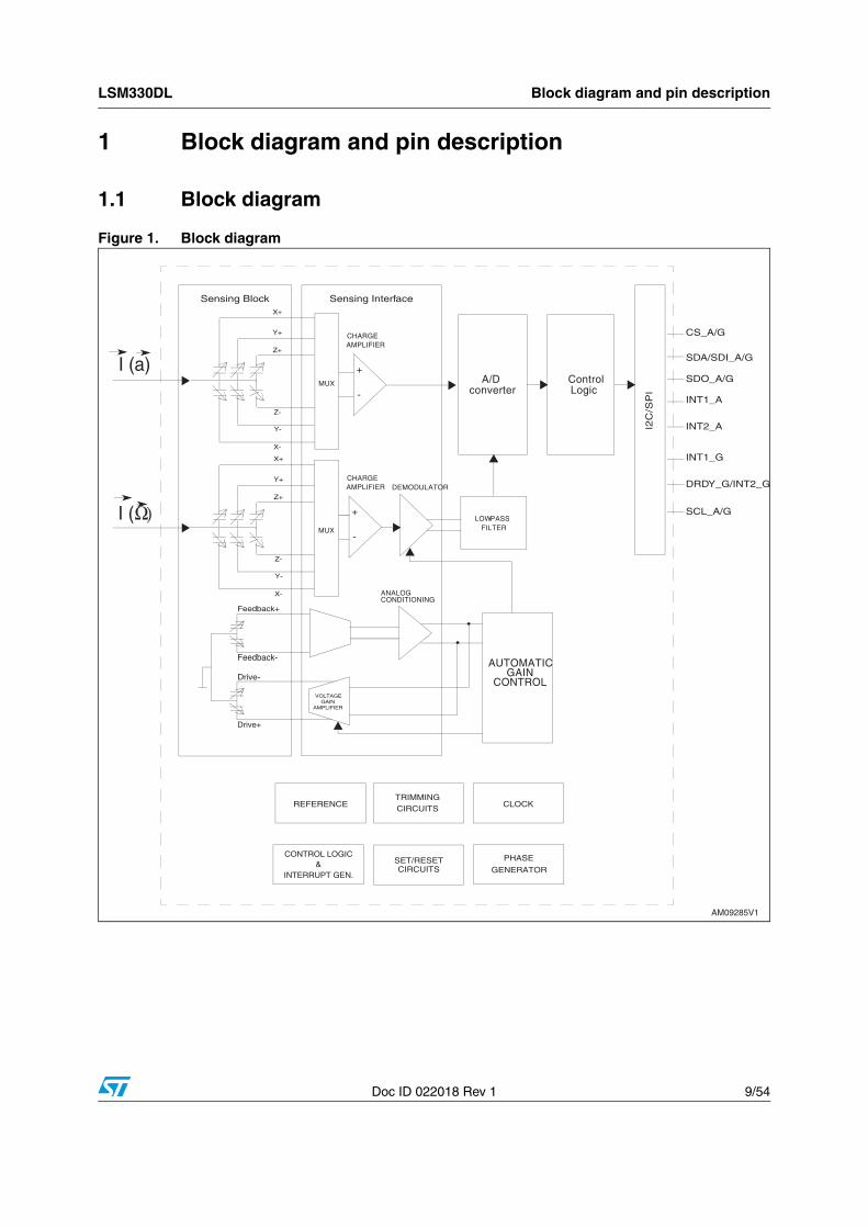
LSM330DL Block diagram and pin description
Doc ID 022018 Rev 1 9/54
1 Block diagram and pin description
1.1 Block diagram
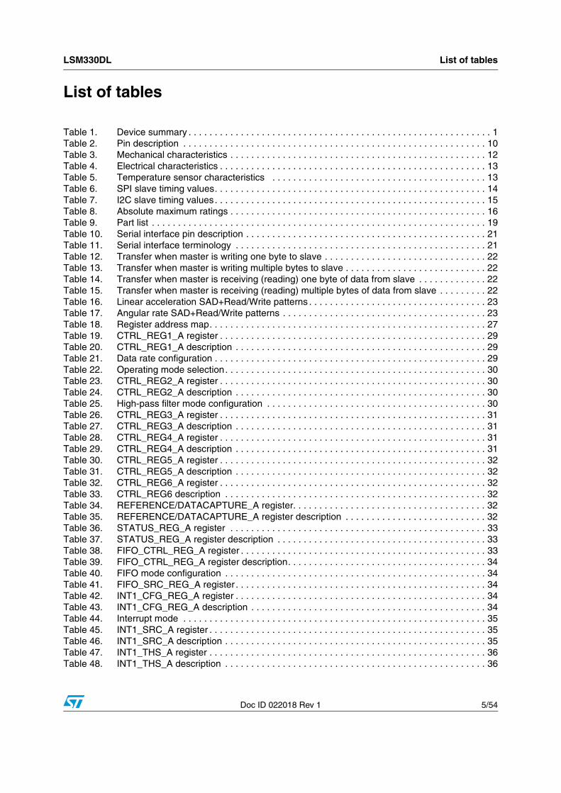
Figure 1. Block diagram
Y+
Z+
Y-
Z-
X+
X-
MUX
CS_A/G
SDA/SDI_A/G
SDO_A/GI (a) +
-
CHARGEAMPLIFIER
Sensing Block Sensing Interface
A/D Control Logicconverter
I2C
/SP
I
INT1_A
INT2_A
I (Ω)
Drive+
Drive-
Feedback+
Feedback-
DEMODULATOR
VOLTAGE
AUTOMATICGAIN
CONTROL
LOW-PASSFILTER
GAINAMPLIFIER
ANALOGCONDITIONING
CONTROL LOGIC&
INTERRUPT GEN.
CLOCKTRIMMINGCIRCUITSREFERENCE
SET/RESETCIRCUITS GENERATOR
PHASE
+
-
CHARGEAMPLIFIER
Y+
Z+
Y-
Z-
X+
X-
MUX
INT1_G
DRDY_G/INT2_G
SCL_A/G
AM09285V1

Block diagram and pin description LSM330DL
10/54 Doc ID 022018 Rev 1
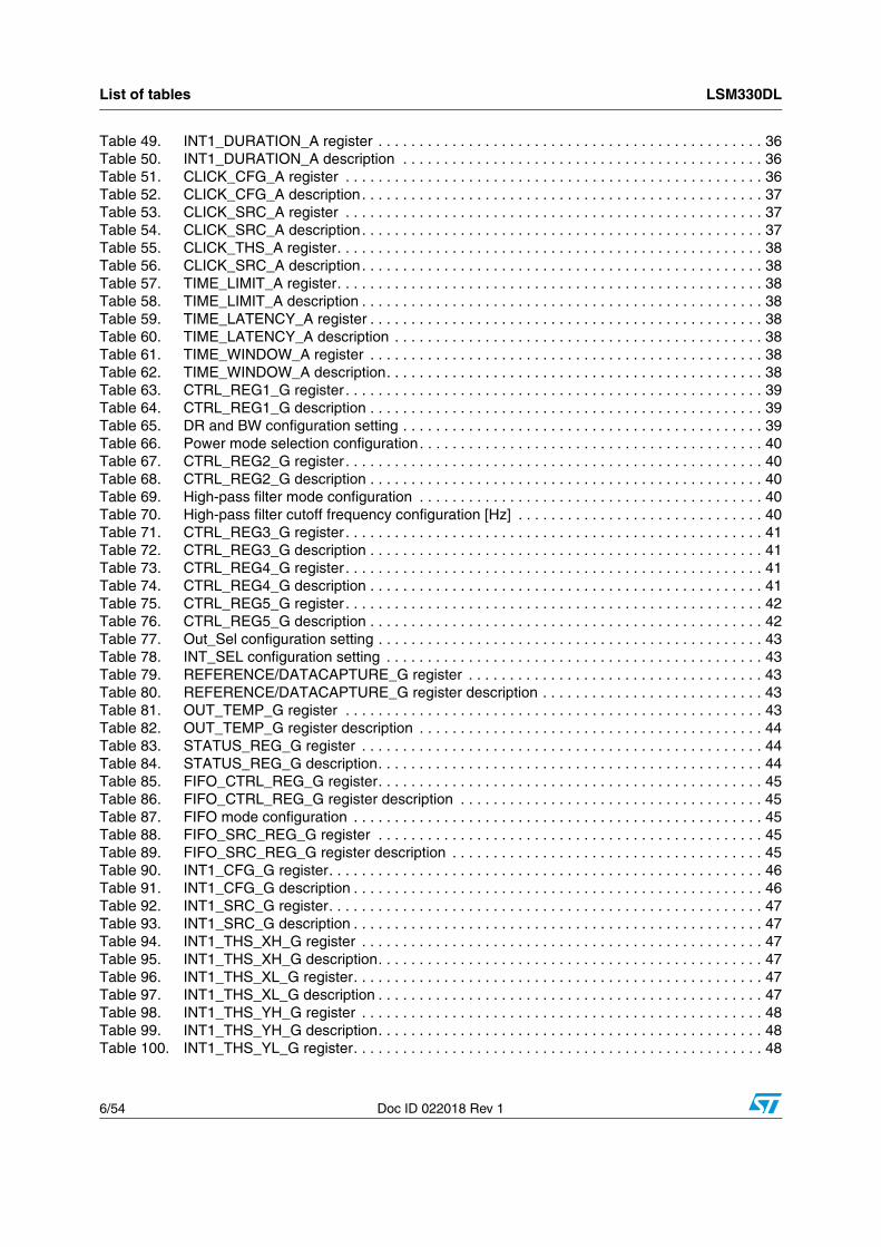
1.2 Pin description
Figure 2. Pin connections
Y1
X
Z
DIRECTION OFDETECTABLEACCELERATIONS
Z
DIRECTION OFDETECTABLEANGULAR RATE
1
+ΩX
+Ωz+ΩY
Y
FILTVDD
FILTIN Y
(BOTTOM VIEW)
24
1
SD
O_A
SD
A/S
DI_
G
INT
1_A
SD
A/S
DI_
A
LSM330DL
Res
28
CS
_G
DR
DY
_G/IN
T2_
G
10
15
11
1425
INT
2_A
SD
O_G
Res
Vdd_IO_A
VCONT
Res
Res
Vdd
CS
_ARes
Res
INT
1_G
Vdd
Res
Res
SC
L_A
GND Res
SCL_G
Vdd_IO_G
Res
X
AM09256V1
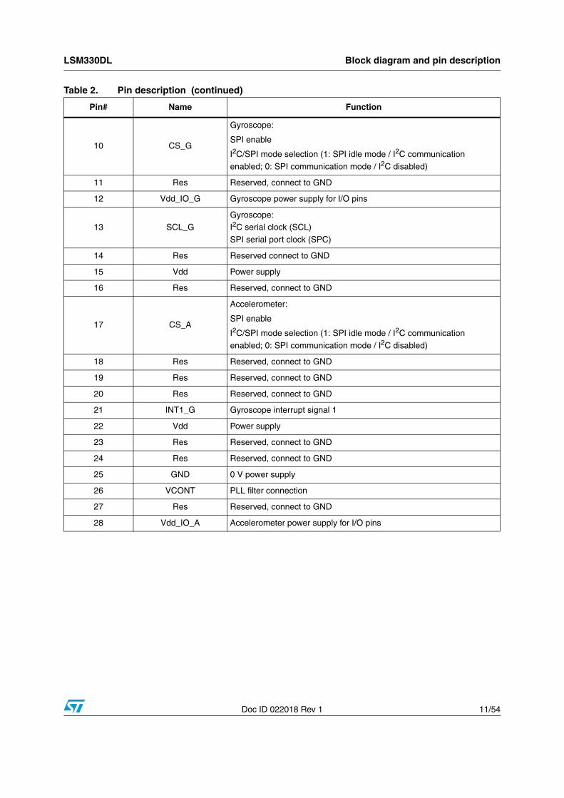
Table 2. Pin description
Pin# Name Function
1 SDA/SDI_A
Accelerometer:
I2C serial data (SDA)
SPI serial data input (SDI)3-wire interface serial data output (SDO)
2 Res Reserved, connect to GND
3 SDO_A
Accelerometer:
SPI serial data output (SDO)I2C least significant bit of the device address (SA0)
4 SCL_AAccelerometer:I2C serial clock (SCL)
SPI serial port clock (SPC)
5 DRDY_G/INT2_G Gyroscope data ready/interrupt signal 2
6 INT1_A Accelerometer interrupt signal
7 SDO_G
Gyroscope:
SPI serial data output (SDO)I2C least significant bit of the device address (SA0)
8 INT2_A Accelerometer interrupt signal
9 SDA/SDI_G
Gyroscope:
I2C serial data (SDA)SPI serial data input (SDI)
3-wire interface serial data output (SDO)
LSM330DL Block diagram and pin description
Doc ID 022018 Rev 1 11/54
10 CS_G
Gyroscope:
SPI enable
I2C/SPI mode selection (1: SPI idle mode / I2C communication
enabled; 0: SPI communication mode / I2C disabled)
11 Res Reserved, connect to GND
12 Vdd_IO_G Gyroscope power supply for I/O pins
13 SCL_GGyroscope:I2C serial clock (SCL)
SPI serial port clock (SPC)
14 Res Reserved connect to GND
15 Vdd Power supply
16 Res Reserved, connect to GND
17 CS_A
Accelerometer:
SPI enable
I2C/SPI mode selection (1: SPI idle mode / I2C communication
enabled; 0: SPI communication mode / I2C disabled)
18 Res Reserved, connect to GND
19 Res Reserved, connect to GND
20 Res Reserved, connect to GND
21 INT1_G Gyroscope interrupt signal 1
22 Vdd Power supply
23 Res Reserved, connect to GND
24 Res Reserved, connect to GND
25 GND 0 V power supply
26 VCONT PLL filter connection
27 Res Reserved, connect to GND
28 Vdd_IO_A Accelerometer power supply for I/O pins
Table 2. Pin description (continued)
Pin# Name Function
Module specifications LSM330DL
12/54 Doc ID 022018 Rev 1
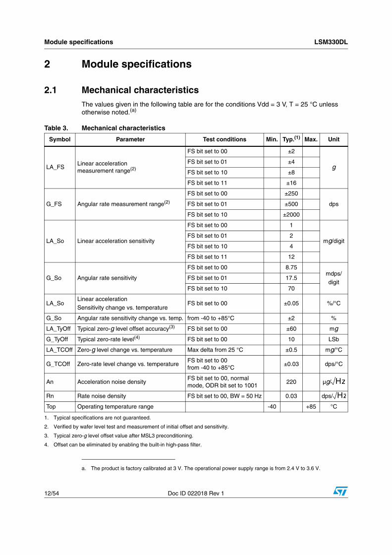
2 Module specifications
2.1 Mechanical characteristicsThe values given in the following table are for the conditions Vdd = 3 V, T = 25 °C unless otherwise noted.(a)
a. The product is factory calibrated at 3 V. The operational power supply range is from 2.4 V to 3.6 V.
Table 3. Mechanical characteristics
Symbol Parameter Test conditions Min. Typ.(1) Max. Unit
LA_FSLinear acceleration measurement range(2)
FS bit set to 00 ±2
gFS bit set to 01 ±4
FS bit set to 10 ±8
FS bit set to 11 ±16
G_FS Angular rate measurement range(2)
FS bit set to 00 ±250
dpsFS bit set to 01 ±500
FS bit set to 10 ±2000
LA_So Linear acceleration sensitivity
FS bit set to 00 1
mg/digitFS bit set to 01 2
FS bit set to 10 4
FS bit set to 11 12
G_So Angular rate sensitivity
FS bit set to 00 8.75mdps/
digitFS bit set to 01 17.5
FS bit set to 10 70
LA_SoLinear acceleration
Sensitivity change vs. temperatureFS bit set to 00 ±0.05 %/°C
G_So Angular rate sensitivity change vs. temp. from -40 to +85°C ±2 %
LA_TyOff Typical zero-g level offset accuracy(3) FS bit set to 00 ±60 mg
G_TyOff Typical zero-rate level(4) FS bit set to 00 10 LSb
LA_TCOff Zero-g level change vs. temperature Max delta from 25 °C ±0.5 mg/°C
G_TCOff Zero-rate level change vs. temperatureFS bit set to 00 from -40 to +85°C
±0.03 dps/°C
An Acceleration noise densityFS bit set to 00, normal mode, ODR bit set to 1001
220 µg/
Rn Rate noise density FS bit set to 00, BW = 50 Hz 0.03 dps/
Top Operating temperature range -40 +85 °C
1. Typical specifications are not guaranteed.
2. Verified by wafer level test and measurement of initial offset and sensitivity.
3. Typical zero-g level offset value after MSL3 preconditioning.
4. Offset can be eliminated by enabling the built-in high-pass filter.
Hz
Hz
LSM330DL Module specifications
Doc ID 022018 Rev 1 13/54
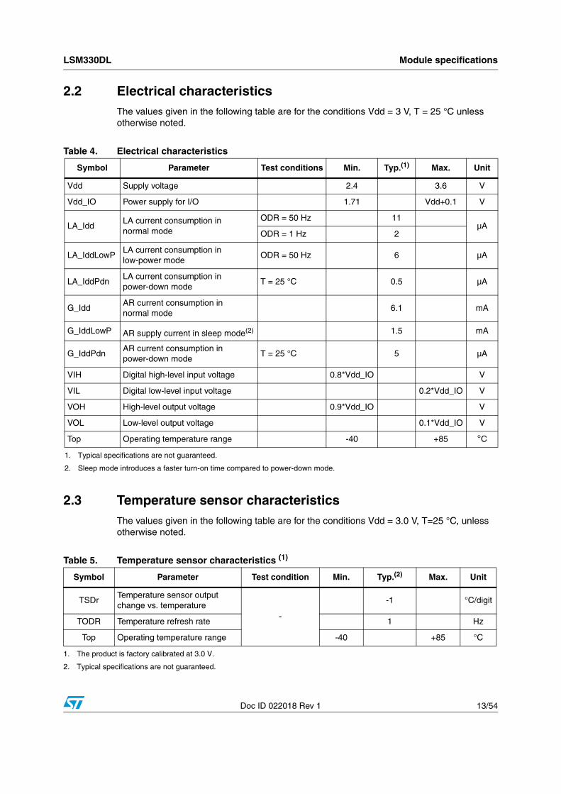
2.2 Electrical characteristicsThe values given in the following table are for the conditions Vdd = 3 V, T = 25 °C unless otherwise noted.
2.3 Temperature sensor characteristicsThe values given in the following table are for the conditions Vdd = 3.0 V, T=25 °C, unless otherwise noted.
Table 4. Electrical characteristics
Symbol Parameter Test conditions Min. Typ.(1) Max. Unit
Vdd Supply voltage 2.4 3.6 V
Vdd_IO Power supply for I/O 1.71 Vdd+0.1 V
LA_IddLA current consumption innormal mode
ODR = 50 Hz 11µA
ODR = 1 Hz 2
LA_IddLowPLA current consumption in low-power mode
ODR = 50 Hz 6 µA
LA_IddPdnLA current consumption in power-down mode
T = 25 °C 0.5 µA
G_IddAR current consumption innormal mode
6.1 mA
G_IddLowP AR supply current in sleep mode(2) 1.5 mA
G_IddPdnAR current consumption in power-down mode
T = 25 °C 5 µA
VIH Digital high-level input voltage 0.8*Vdd_IO V
VIL Digital low-level input voltage 0.2*Vdd_IO V
VOH High-level output voltage 0.9*Vdd_IO V
VOL Low-level output voltage 0.1*Vdd_IO V
Top Operating temperature range -40 +85 °C
1. Typical specifications are not guaranteed.
2. Sleep mode introduces a faster turn-on time compared to power-down mode.
Table 5. Temperature sensor characteristics (1)
Symbol Parameter Test condition Min. Typ.(2) Max. Unit
TSDrTemperature sensor output change vs. temperature
-
-1 °C/digit
TODR Temperature refresh rate 1 Hz
Top Operating temperature range -40 +85 °C
1. The product is factory calibrated at 3.0 V.
2. Typical specifications are not guaranteed.
Module specifications LSM330DL
14/54 Doc ID 022018 Rev 1
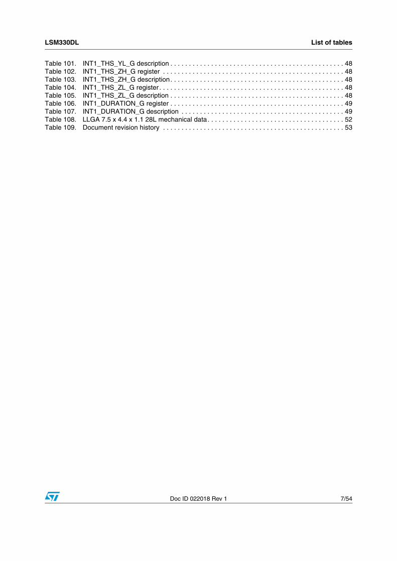
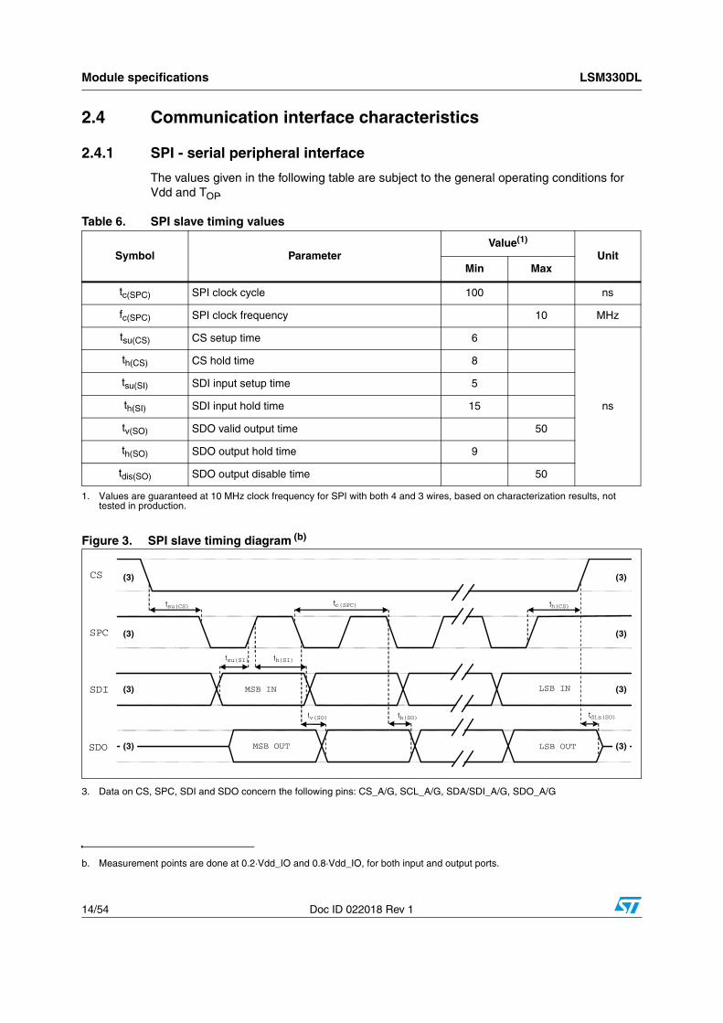
2.4 Communication interface characteristics
2.4.1 SPI - serial peripheral interface
The values given in the following table are subject to the general operating conditions for Vdd and TOP.
Figure 3. SPI slave timing diagram (b)
3. Data on CS, SPC, SDI and SDO concern the following pins: CS_A/G, SCL_A/G, SDA/SDI_A/G, SDO_A/G
Table 6. SPI slave timing values
Symbol ParameterValue(1)
UnitMin Max
tc(SPC) SPI clock cycle 100 ns
fc(SPC) SPI clock frequency 10 MHz
tsu(CS) CS setup time 6
ns
th(CS) CS hold time 8
tsu(SI) SDI input setup time 5
th(SI) SDI input hold time 15
tv(SO) SDO valid output time 50
th(SO) SDO output hold time 9
tdis(SO) SDO output disable time 50
1. Values are guaranteed at 10 MHz clock frequency for SPI with both 4 and 3 wires, based on characterization results, not tested in production.
b. Measurement points are done at 0.2·Vdd_IO and 0.8·Vdd_IO, for both input and output ports.
SPC
CS
SDI
SDO
tsu(CS)
tv(SO) th(SO)
th(SI)tsu(SI)
th(CS)
tdis(SO)
tc(SPC)
MSB IN
MSB OUT LSB OUT
LSB IN
(3)
(3)
(3)
(3)
(3)
(3)
(3)
(3)
LSM330DL Module specifications
Doc ID 022018 Rev 1 15/54
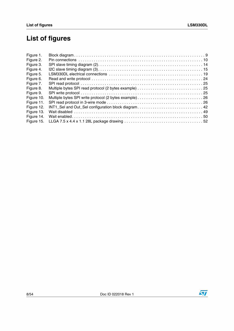
2.4.2 I2C - inter-IC control interface
The values given in the following table are subject to the general operating conditions for Vdd and TOP.
Figure 4. I2C slave timing diagram (3)
1. Data based on standard I2C protocol requirement, not tested in production.
2 Cb = total capacitance of one bus line, in pF
3. Measurement points are done at 0.2·Vdd_IO and 0.8·Vdd_IO, for both ports.
Table 7. I2C slave timing values
Symbol Parameter(1)I2C standard mode I2C fast mode (1)
UnitMin Max Min Max
f(SCL) SCL clock frequency 0 100 0 400 kHz
tw(SCLL) SCL clock low time 4.7 1.3µs
tw(SCLH) SCL clock high time 4.0 0.6
tsu(SDA) SDA setup time 250 100 ns
th(SDA) SDA data hold time 0.01 3.45 0 0.9 µs
tr(SDA) tr(SCL) SDA and SCL rise time 1000 20 + 0.1Cb (2) 300
nstf(SDA) tf(SCL) SDA and SCL fall time 300 20 + 0.1Cb
(2) 300
th(ST) START condition hold time 4 0.6
µs
tsu(SR) Repeated START condition setup time 4.7 0.6
tsu(SP) STOP condition setup time 4 0.6
tw(SP:SR)Bus free time between STOP and START condition
4.7 1.3
1. SCL (SCL_A/G pin), SDA (SDA_A/G pin)
SDA
SCL
tf(SDA)
tsu(SP)
tw(SCLL)
tsu(SDA)tr(SDA)
tsu(SR)
th(ST) tw(SCLH)
th(SDA)
tr(SCL) tf(SCL)
tw(SP:SR)
START
REPEATEDSTART
STOP
START
AM09238V1
Module specifications LSM330DL
16/54 Doc ID 022018 Rev 1
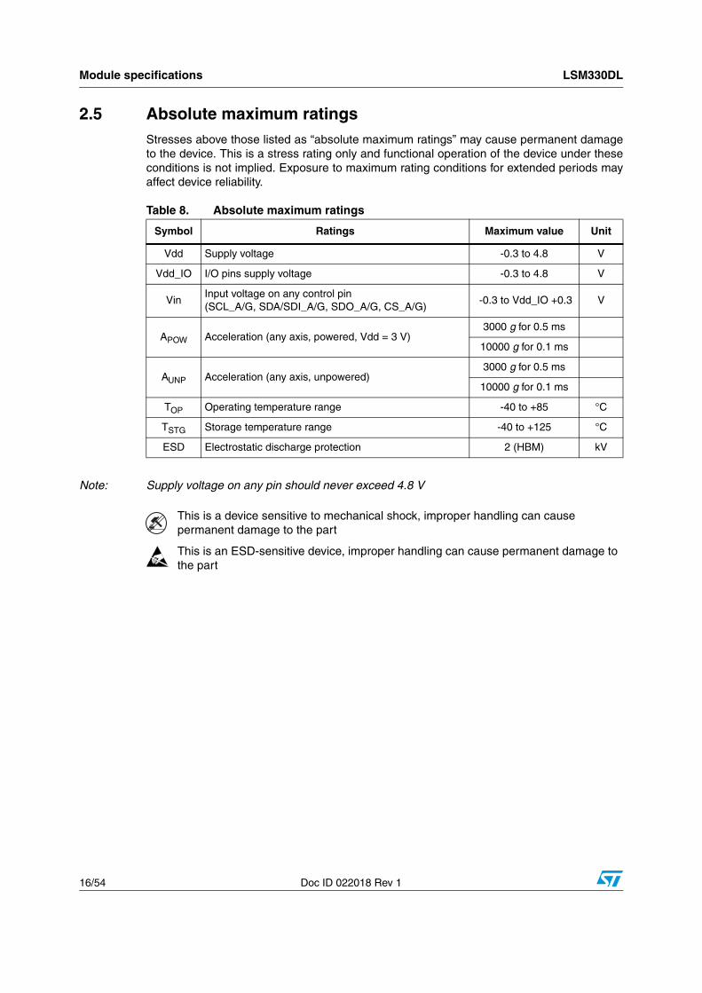
2.5 Absolute maximum ratingsStresses above those listed as “absolute maximum ratings” may cause permanent damageto the device. This is a stress rating only and functional operation of the device under theseconditions is not implied. Exposure to maximum rating conditions for extended periods mayaffect device reliability.
Note: Supply voltage on any pin should never exceed 4.8 V
Table 8. Absolute maximum ratings
Symbol Ratings Maximum value Unit
Vdd Supply voltage -0.3 to 4.8 V
Vdd_IO I/O pins supply voltage -0.3 to 4.8 V
VinInput voltage on any control pin (SCL_A/G, SDA/SDI_A/G, SDO_A/G, CS_A/G)
-0.3 to Vdd_IO +0.3 V
APOW Acceleration (any axis, powered, Vdd = 3 V)3000 g for 0.5 ms
10000 g for 0.1 ms
AUNP Acceleration (any axis, unpowered)3000 g for 0.5 ms
10000 g for 0.1 ms
TOP Operating temperature range -40 to +85 °C
TSTG Storage temperature range -40 to +125 °C
ESD Electrostatic discharge protection 2 (HBM) kV
This is a device sensitive to mechanical shock, improper handling can cause permanent damage to the part
This is an ESD-sensitive device, improper handling can cause permanent damage to the part

LSM330DL Module specifications
Doc ID 022018 Rev 1 17/54
2.6 Terminology
2.6.1 Sensitivity
Linear acceleration sensitivity can be determined by applying 1 g acceleration to the device. As the sensor can measure DC accelerations, this can be done easily by pointing the axis of interest towards the center of the Earth, noting the output value, rotating the sensor by 180 degrees (point to the sky) and then noting the output value again. By doing so, ±1 g acceleration is applied to the sensor. Subtracting the larger output value from the smaller one, and dividing the result by 2, leads to the actual sensitivity of the sensor. This value changes very little over temperature and also very little over time. The sensitivity tolerance describes the range of sensitivities of a large population of sensors.
Angular rate sensitivity describes the angular rate gain of the sensor and can be determined by applying a defined angular velocity to it. This value changes very little over temperature and also very little over time.
2.6.2 Zero level
Linear acceleration zero-g level offset (TyOff) describes the deviation of an actual output signal from the ideal output signal if no acceleration is present. A sensor in a steady state on a horizontal surface will measure 0 g on the X-axis and 0 g on the Y-axis whereas the Z-axis will measure 1 g. The output is ideally in the middle of the dynamic range of the sensor (content of OUT registers 00h, data expressed as 2’s complement number). A deviation from the ideal value in this case is called zero-g offset. Offset is to some extent a result of stress to the MEMS sensor and therefore the offset can slightly change after mounting the sensor onto a printed circuit board or exposing it to extensive mechanical stress. Offset changes little over temperature, see “Zero-g level change vs. temperature” (refer toTable 3). The zero-g level tolerance (TyOff) describes the standard deviation of the range of zero-g levels of a population of sensors.
The angular rate zero-rate level describes the actual output value if there is no angular rate present. Zero-rate level of precise MEMS sensors is, to some extent, a result of stress to the sensor and therefore the zero-rate level can slightly change after mounting the sensor onto a printed circuit board or after exposing it to extensive mechanical stress. This value changes very little over temperature and also very little over time.

Functionality LSM330DL
18/54 Doc ID 022018 Rev 1
3 Functionality
The LSM330DL is a system-in-package featuring a 3D digital accelerometer and a 3D digital gyroscope.
The complete device includes specific sensing elements and two IC interfaces able to measure both the acceleration and angular rate applied to the module and to provide a signal to the external world through an SPI/I2C serial interface.
The various sensing elements are manufactured using specialized micromachining processes, while the IC interfaces are based on CMOS technology that allows designing a dedicated circuit which is trimmed to better match the sensing element characteristics.
The LSM330DL may also be configured to generate an inertial wake-up and free-fall interrupt signal according to a programmed acceleration event along the enabled axes.
3.1 Factory calibrationThe IC interface is factory calibrated for sensitivity and zero level. The trimming values are stored inside the device in non-volatile memory. Any time the device is turned on, the trimming parameters are downloaded into the registers to be used during normal operation. This allows using the device without further calibration.
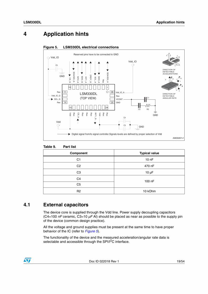
LSM330DL Application hints
Doc ID 022018 Rev 1 19/54
4 Application hints
Figure 5. LSM330DL electrical connections
4.1 External capacitorsThe device core is supplied through the Vdd line. Power supply decoupling capacitors (C4=100 nF ceramic, C3=10 µF Al) should be placed as near as possible to the supply pin of the device (common design practice).
All the voltage and ground supplies must be present at the same time to have proper behavior of the IC (refer to Figure 5).
The functionality of the device and the measured acceleration/angular rate data is selectable and accessible through the SPI/I2C interface.
Table 9. Part list
Component Typical value
C1 10 nF
C2 470 nF
C3 10 µF
C4 100 nF
C5
R2 10 kOhm
Digital signal from/to signal controller.Signals levels are defined by proper selection of Vdd
Y1
X
Z
DIRECTION OFDETECTABLEACCELERATIONS
DIRECTION OFDETECTABLEANGULAR RATE
Vdd_IO
GND
VddC3
C4
FILTVDD
FILTIN Y
(TOP VIEW)
24
1
SD
O_
A
SD
A/S
DI_
G
INT
1_A
SD
A/S
DI_
A
LSM330DL
Re
s
28
CS
_G
DR
DY
_G
10
15
11
14 25
INT
2_
A
SD
O_
G
Re
s
Vdd_IO_A
VCONT
Res
Re
s
Vd
d
CS
_A
Re
s
Re
s
INT
1_
G
Vd
d
Re
s
Re
s
SC
L_
A
GNDRes
SCL_G
Vdd_IO_G
Res
Vdd_IO
C1
R2C2
GND
C5
GND
Reserved pins have to be connected to GND
Z1
+Ω X
+Ω z+Ω Y
Y
X
AM09287v1
Application hints LSM330DL
20/54 Doc ID 022018 Rev 1
The functions, the threshold and the timing of the two interrupt pins for each sensor can be completely programmed by the user though the SPI/I2C interface.
4.2 Soldering informationThe LGA package is compliant with the ECOPACK®, RoHS and “Green” standards. It is qualified for soldering heat resistance according to JEDEC J-STD-020D.
Leave “Pin 1 Indicator” unconnected during soldering.
The landing pattern and soldering recommendations are available at www.st.com/mems.
LSM330DL Digital interfaces
Doc ID 022018 Rev 1 21/54
5 Digital interfaces
The registers embedded inside the LSM330DL may be accessed through both the I2C andSPI serial interfaces. The latter may be SW configured to operate either in 3-wire or 4-wireinterface mode.
To select/exploit the I2C interface, the CS line must be tied high (i.e. connected to Vdd_IO).
5.1 I2C serial interfaceThe LSM330DL I2C is a bus slave. The I2C is employed to write data into the registers whose content can also be read back.
The relevant I2C terminology is given in the table below.
There are two signals associated with the I2C bus: the serial clock line (SCL) and the serial data line (SDA). The latter is a bidirectional line used for sending and receiving the data to/from the interface.
Table 10. Serial interface pin description
Pin name Pin description
CS_ALinear acceleration SPI enableLinear acceleration I2C/SPI mode selection (1: I2C mode; 0: SPI enabled)
CS_GAngular rate SPI enableAngular rate I2C/SPI mode selection (1: I2C mode; 0: SPI enabled)
SCL_A
SCL_G
I2C serial clock (SCL)
SPI serial port clock (SPC)
SDA/SDI_A
SDA/SDI_G
I2C serial data (SDA)
SPI serial data input (SDI)3-wire interface serial data output (SDO)
SDO_ASDO_G
I2C least significant bit of the device address (SA0)SPI serial data output (SDO)
Table 11. Serial interface terminology
Term Description
Transmitter The device which sends data to the bus
Receiver The device which receives data from the bus
MasterThe device which initiates a transfer, generates clock signals and terminates a transfer
Slave The device addressed by the master
Digital interfaces LSM330DL
22/54 Doc ID 022018 Rev 1
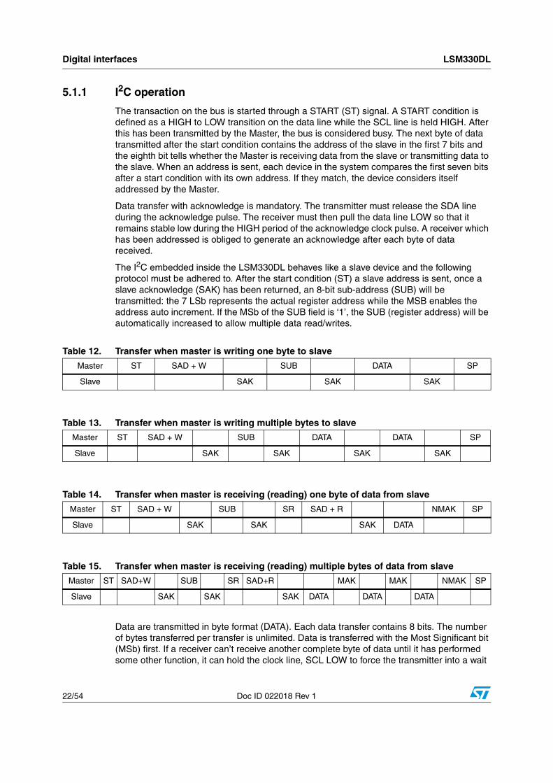
5.1.1 I2C operation
The transaction on the bus is started through a START (ST) signal. A START condition is defined as a HIGH to LOW transition on the data line while the SCL line is held HIGH. After this has been transmitted by the Master, the bus is considered busy. The next byte of data transmitted after the start condition contains the address of the slave in the first 7 bits and the eighth bit tells whether the Master is receiving data from the slave or transmitting data to the slave. When an address is sent, each device in the system compares the first seven bits after a start condition with its own address. If they match, the device considers itself addressed by the Master.
Data transfer with acknowledge is mandatory. The transmitter must release the SDA line during the acknowledge pulse. The receiver must then pull the data line LOW so that it remains stable low during the HIGH period of the acknowledge clock pulse. A receiver which has been addressed is obliged to generate an acknowledge after each byte of data received.
The I2C embedded inside the LSM330DL behaves like a slave device and the following protocol must be adhered to. After the start condition (ST) a slave address is sent, once a slave acknowledge (SAK) has been returned, an 8-bit sub-address (SUB) will be transmitted: the 7 LSb represents the actual register address while the MSB enables the address auto increment. If the MSb of the SUB field is ‘1’, the SUB (register address) will be automatically increased to allow multiple data read/writes.
Data are transmitted in byte format (DATA). Each data transfer contains 8 bits. The number of bytes transferred per transfer is unlimited. Data is transferred with the Most Significant bit (MSb) first. If a receiver can’t receive another complete byte of data until it has performed some other function, it can hold the clock line, SCL LOW to force the transmitter into a wait
Table 12. Transfer when master is writing one byte to slave
Master ST SAD + W SUB DATA SP
Slave SAK SAK SAK
Table 13. Transfer when master is writing multiple bytes to slave
Master ST SAD + W SUB DATA DATA SP
Slave SAK SAK SAK SAK
Table 14. Transfer when master is receiving (reading) one byte of data from slave
Master ST SAD + W SUB SR SAD + R NMAK SP
Slave SAK SAK SAK DATA
Table 15. Transfer when master is receiving (reading) multiple bytes of data from slave
Master ST SAD+W SUB SR SAD+R MAK MAK NMAK SP
Slave SAK SAK SAK DATA DATA DATA
LSM330DL Digital interfaces
Doc ID 022018 Rev 1 23/54
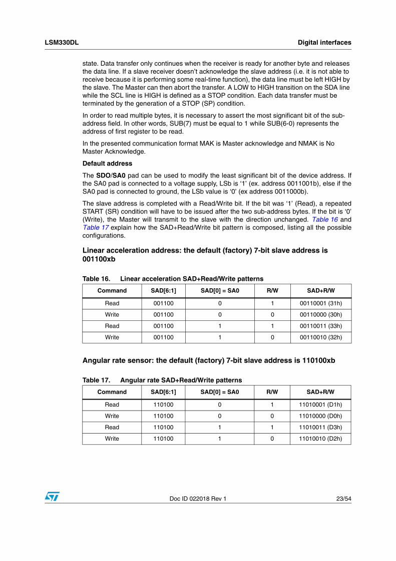
state. Data transfer only continues when the receiver is ready for another byte and releases the data line. If a slave receiver doesn’t acknowledge the slave address (i.e. it is not able to receive because it is performing some real-time function), the data line must be left HIGH by the slave. The Master can then abort the transfer. A LOW to HIGH transition on the SDA line while the SCL line is HIGH is defined as a STOP condition. Each data transfer must be terminated by the generation of a STOP (SP) condition.
In order to read multiple bytes, it is necessary to assert the most significant bit of the sub-address field. In other words, SUB(7) must be equal to 1 while SUB(6-0) represents the address of first register to be read.
In the presented communication format MAK is Master acknowledge and NMAK is No Master Acknowledge.
Default address
The SDO/SA0 pad can be used to modify the least significant bit of the device address. Ifthe SA0 pad is connected to a voltage supply, LSb is ‘1’ (ex. address 0011001b), else if theSA0 pad is connected to ground, the LSb value is ‘0’ (ex address 0011000b).
The slave address is completed with a Read/Write bit. If the bit was ‘1’ (Read), a repeatedSTART (SR) condition will have to be issued after the two sub-address bytes. If the bit is ‘0’(Write), the Master will transmit to the slave with the direction unchanged. Table 16 andTable 17 explain how the SAD+Read/Write bit pattern is composed, listing all the possibleconfigurations.
Linear acceleration address: the default (factory) 7-bit slave address is 001100xb
Angular rate sensor: the default (factory) 7-bit slave address is 110100xb
Table 16. Linear acceleration SAD+Read/Write patterns
Command SAD[6:1] SAD[0] = SA0 R/W SAD+R/W
Read 001100 0 1 00110001 (31h)
Write 001100 0 0 00110000 (30h)
Read 001100 1 1 00110011 (33h)
Write 001100 1 0 00110010 (32h)
Table 17. Angular rate SAD+Read/Write patterns
Command SAD[6:1] SAD[0] = SA0 R/W SAD+R/W
Read 110100 0 1 11010001 (D1h)
Write 110100 0 0 11010000 (D0h)
Read 110100 1 1 11010011 (D3h)
Write 110100 1 0 11010010 (D2h)
Digital interfaces LSM330DL
24/54 Doc ID 022018 Rev 1
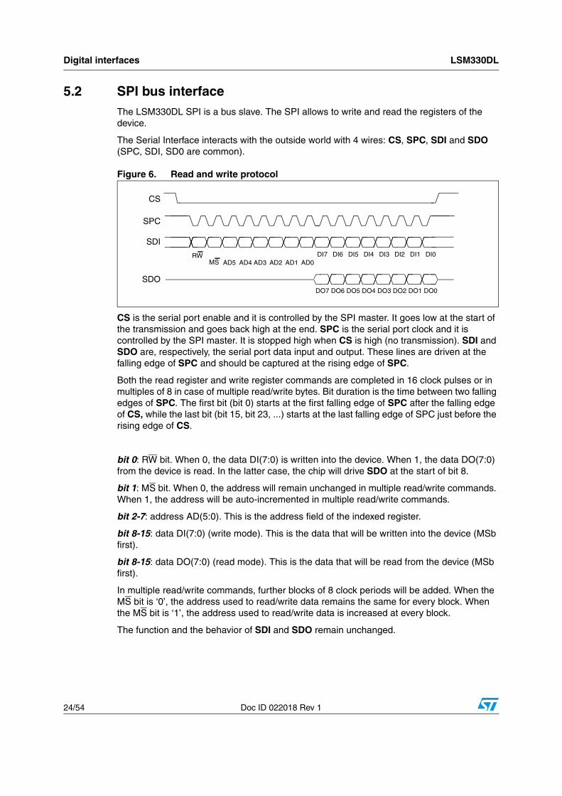
5.2 SPI bus interfaceThe LSM330DL SPI is a bus slave. The SPI allows to write and read the registers of the device.
The Serial Interface interacts with the outside world with 4 wires: CS, SPC, SDI and SDO (SPC, SDI, SD0 are common).
Figure 6. Read and write protocol
CS is the serial port enable and it is controlled by the SPI master. It goes low at the start of the transmission and goes back high at the end. SPC is the serial port clock and it is controlled by the SPI master. It is stopped high when CS is high (no transmission). SDI and SDO are, respectively, the serial port data input and output. These lines are driven at the falling edge of SPC and should be captured at the rising edge of SPC.
Both the read register and write register commands are completed in 16 clock pulses or in multiples of 8 in case of multiple read/write bytes. Bit duration is the time between two falling edges of SPC. The first bit (bit 0) starts at the first falling edge of SPC after the falling edge of CS, while the last bit (bit 15, bit 23, ...) starts at the last falling edge of SPC just before the rising edge of CS.
bit 0: RW bit. When 0, the data DI(7:0) is written into the device. When 1, the data DO(7:0) from the device is read. In the latter case, the chip will drive SDO at the start of bit 8.
bit 1: MS bit. When 0, the address will remain unchanged in multiple read/write commands. When 1, the address will be auto-incremented in multiple read/write commands.
bit 2-7: address AD(5:0). This is the address field of the indexed register.
bit 8-15: data DI(7:0) (write mode). This is the data that will be written into the device (MSb first).
bit 8-15: data DO(7:0) (read mode). This is the data that will be read from the device (MSb first).
In multiple read/write commands, further blocks of 8 clock periods will be added. When the MS bit is ‘0’, the address used to read/write data remains the same for every block. When the MS bit is ‘1’, the address used to read/write data is increased at every block.
The function and the behavior of SDI and SDO remain unchanged.
CS
SPC
SDI
SDO
RWAD5 AD4 AD3 AD2 AD1 AD0
DI7 DI6 DI5 DI4 DI3 DI2 DI1 DI0
DO7 DO6 DO5 DO4 DO3 DO2 DO1 DO0
MS
LSM330DL Digital interfaces
Doc ID 022018 Rev 1 25/54
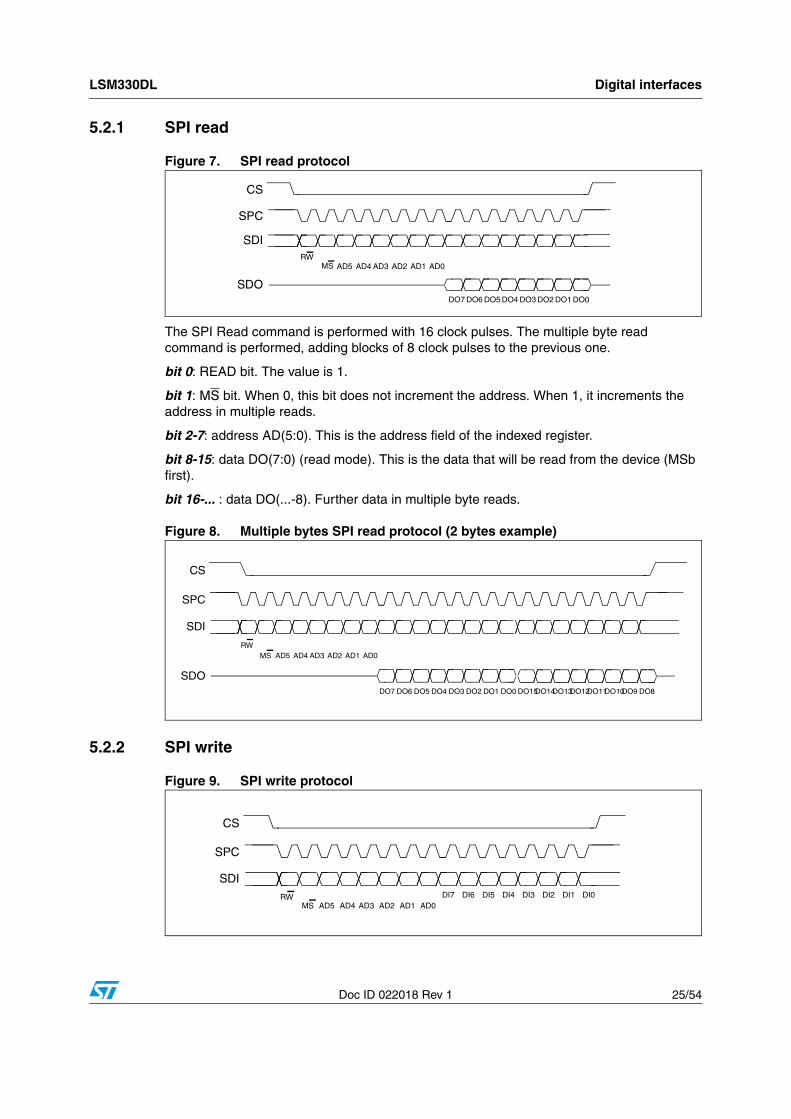
5.2.1 SPI read
Figure 7. SPI read protocol
The SPI Read command is performed with 16 clock pulses. The multiple byte read command is performed, adding blocks of 8 clock pulses to the previous one.
bit 0: READ bit. The value is 1.
bit 1: MS bit. When 0, this bit does not increment the address. When 1, it increments the address in multiple reads.
bit 2-7: address AD(5:0). This is the address field of the indexed register.
bit 8-15: data DO(7:0) (read mode). This is the data that will be read from the device (MSb first).
bit 16-... : data DO(...-8). Further data in multiple byte reads.
Figure 8. Multiple bytes SPI read protocol (2 bytes example)
5.2.2 SPI write
Figure 9. SPI write protocol
CS
SPC
SDI
SDO
RW
DO7 DO6 DO5 DO4 DO3 DO2 DO1 DO0
AD5 AD4 AD3 AD2 AD1 AD0MS
CS
SPC
SDI
SDO
RW
DO7 DO6 DO5 DO4 DO3 DO2 DO1 DO0
AD5 AD4 AD3 AD2 AD1 AD0
DO15 DO14 DO13 DO12 DO11 DO10 DO9 DO8
MS
CS
SPC
SDIRW DI7 DI6 DI5 DI4 DI3 DI2 DI1 DI0
AD5 AD4 AD3 AD2 AD1 AD0MS
Digital interfaces LSM330DL
26/54 Doc ID 022018 Rev 1
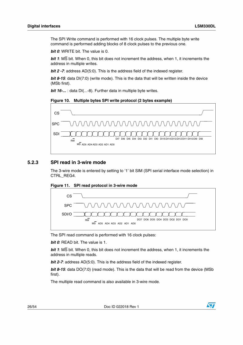
The SPI Write command is performed with 16 clock pulses. The multiple byte write command is performed adding blocks of 8 clock pulses to the previous one.
bit 0: WRITE bit. The value is 0.
bit 1: MS bit. When 0, this bit does not increment the address, when 1, it increments the address in multiple writes.
bit 2 -7: address AD(5:0). This is the address field of the indexed register.
bit 8-15: data DI(7:0) (write mode). This is the data that will be written inside the device (MSb first).
bit 16-... : data DI(...-8). Further data in multiple byte writes.
Figure 10. Multiple bytes SPI write protocol (2 bytes example)
5.2.3 SPI read in 3-wire mode
The 3-wire mode is entered by setting to ‘1’ bit SIM (SPI serial interface mode selection) in CTRL_REG4.
Figure 11. SPI read protocol in 3-wire mode
The SPI read command is performed with 16 clock pulses:
bit 0: READ bit. The value is 1.
bit 1: MS bit. When 0, this bit does not increment the address, when 1, it increments the address in multiple reads.
bit 2-7: address AD(5:0). This is the address field of the indexed register.
bit 8-15: data DO(7:0) (read mode). This is the data that will be read from the device (MSb first).
The multiple read command is also available in 3-wire mode.
CS
SPC
SDI
RW
AD5 AD4 AD3 AD2 AD1 AD0
DI7 DI6 DI5 DI4 DI3 DI2 DI1 DI0 DI15 DI14 DI13 DI12 DI11 DI10 DI9 DI8
MS
CS
SPC
SDI/O
RW DO7 DO6 DO5 DO4 DO3 DO2 DO1 DO0
AD5 AD4 AD3 AD2 AD1 AD0MS
LSM330DL Register mapping
Doc ID 022018 Rev 1 27/54
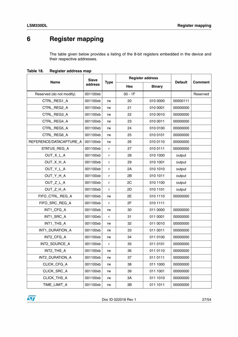
6 Register mapping
The table given below provides a listing of the 8-bit registers embedded in the device andtheir respective addresses.
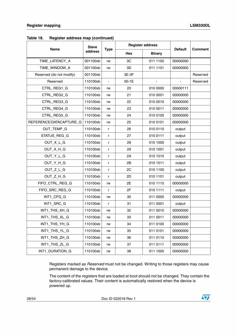
Table 18. Register address map
NameSlave
addressType
Register addressDefault Comment
Hex Binary
Reserved (do not modify) 001100xb 00 - 1F Reserved
CTRL_REG1_A 001100xb rw 20 010 0000 00000111
CTRL_REG2_A 001100xb rw 21 010 0001 00000000
CTRL_REG3_A 001100xb rw 22 010 0010 00000000
CTRL_REG4_A 001100xb rw 23 010 0011 00000000
CTRL_REG5_A 001100xb rw 24 010 0100 00000000
CTRL_REG6_A 001100xb rw 25 010 0101 00000000
REFERENCE/DATACAPTURE_A 001100xb rw 26 010 0110 00000000
STATUS_REG_A 001100xb r 27 010 0111 00000000
OUT_X_L_A 001100xb r 28 010 1000 output
OUT_X_H_A 001100xb r 29 010 1001 output
OUT_Y_L_A 001100xb r 2A 010 1010 output
OUT_Y_H_A 001100xb r 2B 010 1011 output
OUT_Z_L_A 001100xb r 2C 010 1100 output
OUT_Z_H_A 001100xb r 2D 010 1101 output
FIFO_CTRL_REG_A 001100xb rw 2E 010 1110 00000000
FIFO_SRC_REG_A 001100xb r 2F 010 1111
INT1_CFG_A 001100xb rw 30 011 0000 00000000
INT1_SRC_A 001100xb r 31 011 0001 00000000
INT1_THS_A 001100xb rw 32 011 0010 00000000
INT1_DURATION_A 001100xb rw 33 011 0011 00000000
INT2_CFG_A 001100xb rw 34 011 0100 00000000
INT2_SOURCE_A 001100xb r 35 011 0101 00000000
INT2_THS_A 001100xb rw 36 011 0110 00000000
INT2_DURATION_A 001100xb rw 37 011 0111 00000000
CLICK_CFG_A 001100xb rw 38 011 1000 00000000
CLICK_SRC_A 001100xb rw 39 011 1001 00000000
CLICK_THS_A 001100xb rw 3A 011 1010 00000000
TIME_LIMIT_A 001100xb rw 3B 011 1011 00000000
Register mapping LSM330DL
28/54 Doc ID 022018 Rev 1
Registers marked as Reserved must not be changed. Writing to those registers may cause permanent damage to the device.
The content of the registers that are loaded at boot should not be changed. They contain the factory-calibrated values. Their content is automatically restored when the device is powered up.
TIME_LATENCY_A 001100xb rw 3C 011 1100 00000000
TIME_WINDOW_A 001100xb rw 3D 011 1101 00000000
Reserved (do not modify) 001100xb 3E-3F Reserved
Reserved 110100xb - 00-1E - - Reserved
CTRL_REG1_G 110100xb rw 20 010 0000 00000111
CTRL_REG2_G 110100xb rw 21 010 0001 00000000
CTRL_REG3_G 110100xb rw 22 010 0010 00000000
CTRL_REG4_G 110100xb rw 23 010 0011 00000000
CTRL_REG5_G 110100xb rw 24 010 0100 00000000
REFERENCE/DATACAPTURE_G 110100xb rw 25 010 0101 00000000
OUT_TEMP_G 110100xb r 26 010 0110 output
STATUS_REG_G 110100xb r 27 010 0111 output
OUT_X_L_G 110100xb r 28 010 1000 output
OUT_X_H_G 110100xb r 29 010 1001 output
OUT_Y_L_G 110100xb r 2A 010 1010 output
OUT_Y_H_G 110100xb r 2B 010 1011 output
OUT_Z_L_G 110100xb r 2C 010 1100 output
OUT_Z_H_G 110100xb r 2D 010 1101 output
FIFO_CTRL_REG_G 110100xb rw 2E 010 1110 00000000
FIFO_SRC_REG_G 110100xb r 2F 010 1111 output
INT1_CFG_G 110100xb rw 30 011 0000 00000000
INT1_SRC_G 110100xb r 31 011 0001 output
INT1_THS_XH_G 110100xb rw 32 011 0010 00000000
INT1_THS_XL_G 110100xb rw 33 011 0011 00000000
INT1_THS_YH_G 110100xb rw 34 011 0100 00000000
INT1_THS_YL_G 110100xb rw 35 011 0101 00000000
INT1_THS_ZH_G 110100xb rw 36 011 0110 00000000
INT1_THS_ZL_G 110100xb rw 37 011 0111 00000000
INT1_DURATION_G 110100xb rw 38 011 1000 00000000
Table 18. Register address map (continued)
NameSlave
addressType
Register addressDefault Comment
Hex Binary
LSM330DL Registers description
Doc ID 022018 Rev 1 29/54
7 Registers description
The device contains a set of registers which are used to control its behavior and to retrieve acceleration, angular rate and temperature data. The register addresses, composed of 7 bits, are used to identify them and to write the data through the serial interface.
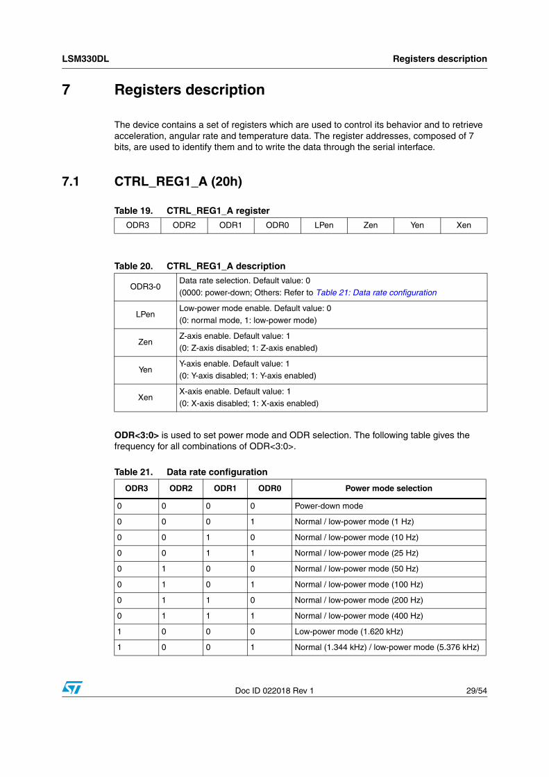
7.1 CTRL_REG1_A (20h)
ODR<3:0> is used to set power mode and ODR selection. The following table gives the frequency for all combinations of ODR<3:0>.
Table 19. CTRL_REG1_A register
ODR3 ODR2 ODR1 ODR0 LPen Zen Yen Xen
Table 20. CTRL_REG1_A description
ODR3-0Data rate selection. Default value: 0
(0000: power-down; Others: Refer to Table 21: Data rate configuration
LPenLow-power mode enable. Default value: 0
(0: normal mode, 1: low-power mode)
ZenZ-axis enable. Default value: 1
(0: Z-axis disabled; 1: Z-axis enabled)
YenY-axis enable. Default value: 1
(0: Y-axis disabled; 1: Y-axis enabled)
XenX-axis enable. Default value: 1
(0: X-axis disabled; 1: X-axis enabled)
Table 21. Data rate configuration
ODR3 ODR2 ODR1 ODR0 Power mode selection
0 0 0 0 Power-down mode
0 0 0 1 Normal / low-power mode (1 Hz)
0 0 1 0 Normal / low-power mode (10 Hz)
0 0 1 1 Normal / low-power mode (25 Hz)
0 1 0 0 Normal / low-power mode (50 Hz)
0 1 0 1 Normal / low-power mode (100 Hz)
0 1 1 0 Normal / low-power mode (200 Hz)
0 1 1 1 Normal / low-power mode (400 Hz)
1 0 0 0 Low-power mode (1.620 kHz)
1 0 0 1 Normal (1.344 kHz) / low-power mode (5.376 kHz)
Registers description LSM330DL
30/54 Doc ID 022018 Rev 1
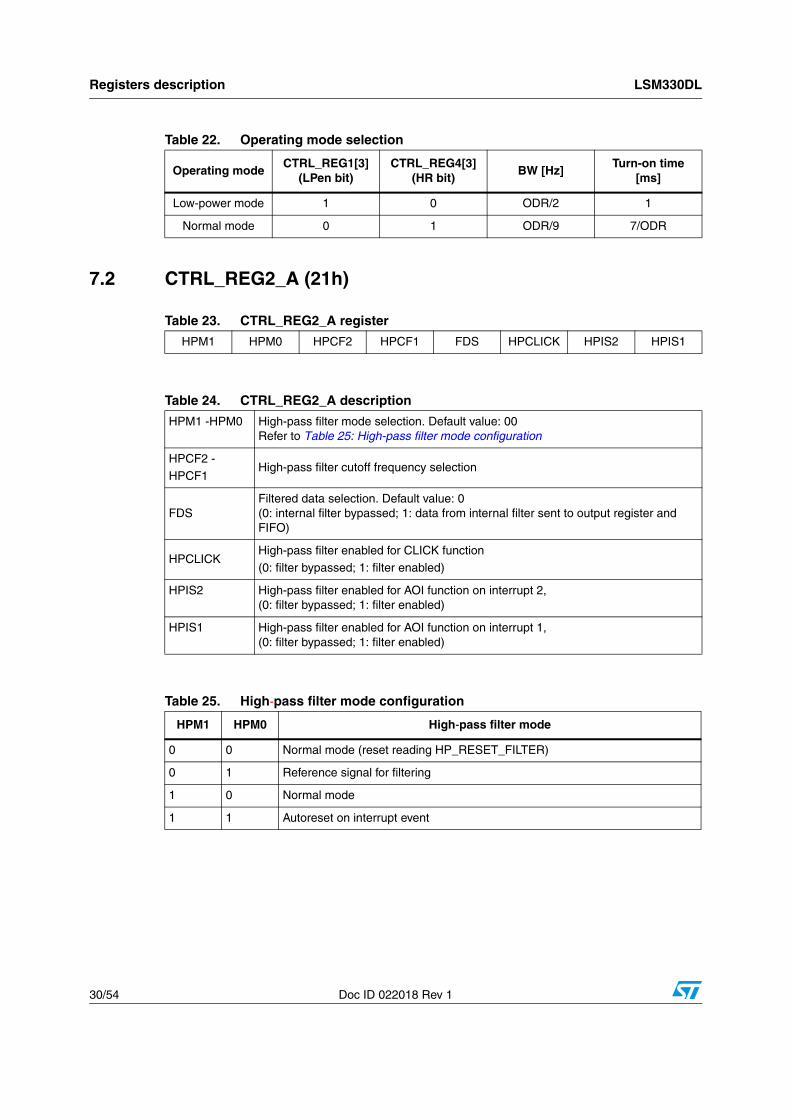
7.2 CTRL_REG2_A (21h)
Table 22. Operating mode selection
Operating modeCTRL_REG1[3]
(LPen bit)CTRL_REG4[3]
(HR bit)BW [Hz]
Turn-on time [ms]
Low-power mode 1 0 ODR/2 1
Normal mode 0 1 ODR/9 7/ODR
Table 23. CTRL_REG2_A register
HPM1 HPM0 HPCF2 HPCF1 FDS HPCLICK HPIS2 HPIS1
Table 24. CTRL_REG2_A description
HPM1 -HPM0 High-pass filter mode selection. Default value: 00Refer to Table 25: High-pass filter mode configuration
HPCF2 -HPCF1
High-pass filter cutoff frequency selection
FDSFiltered data selection. Default value: 0(0: internal filter bypassed; 1: data from internal filter sent to output register and FIFO)
HPCLICKHigh-pass filter enabled for CLICK function(0: filter bypassed; 1: filter enabled)
HPIS2 High-pass filter enabled for AOI function on interrupt 2, (0: filter bypassed; 1: filter enabled)
HPIS1 High-pass filter enabled for AOI function on interrupt 1, (0: filter bypassed; 1: filter enabled)
Table 25. High-pass filter mode configuration
HPM1 HPM0 High-pass filter mode
0 0 Normal mode (reset reading HP_RESET_FILTER)
0 1 Reference signal for filtering
1 0 Normal mode
1 1 Autoreset on interrupt event
LSM330DL Registers description
Doc ID 022018 Rev 1 31/54
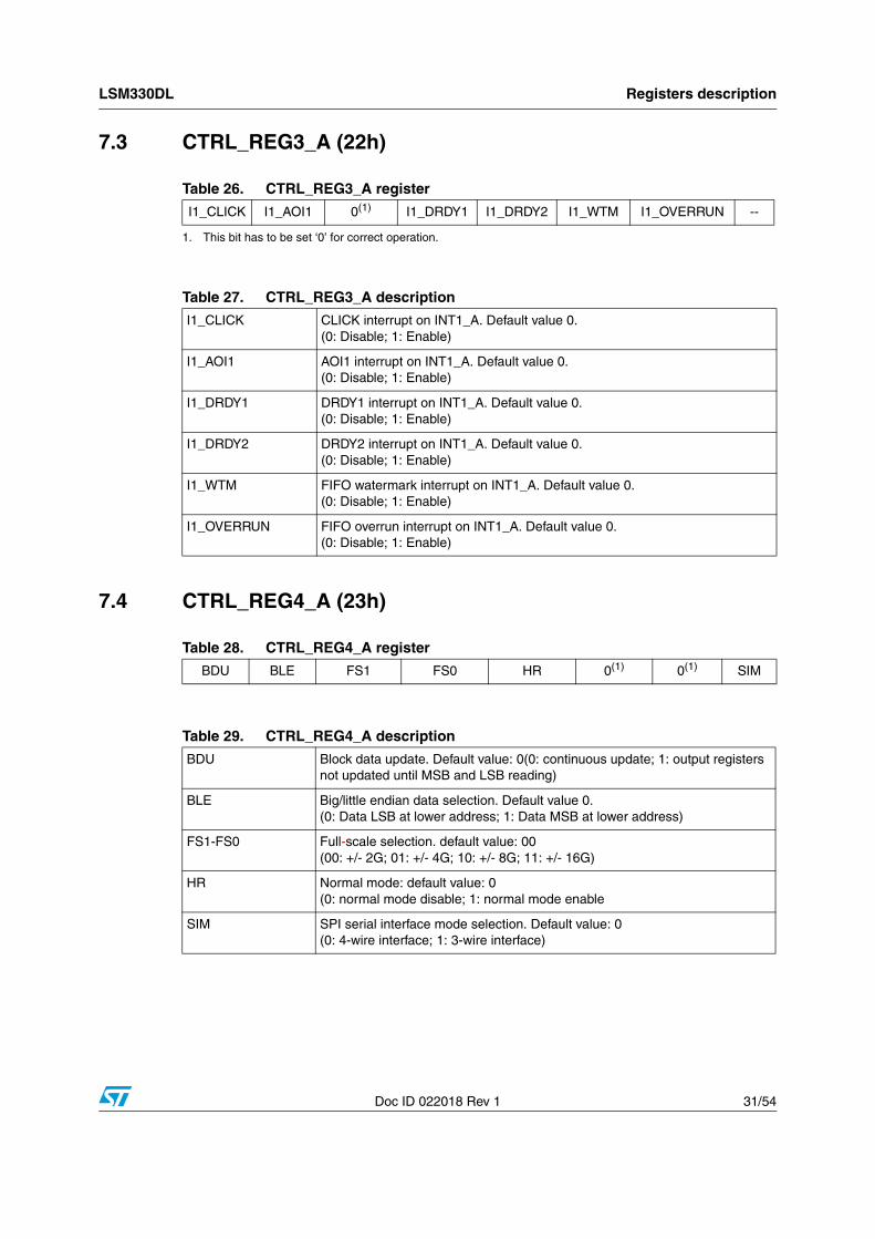
7.3 CTRL_REG3_A (22h)
7.4 CTRL_REG4_A (23h)
Table 26. CTRL_REG3_A register
I1_CLICK I1_AOI1 0(1)
1. This bit has to be set ‘0’ for correct operation.
I1_DRDY1 I1_DRDY2 I1_WTM I1_OVERRUN --
Table 27. CTRL_REG3_A description
I1_CLICK CLICK interrupt on INT1_A. Default value 0.(0: Disable; 1: Enable)
I1_AOI1 AOI1 interrupt on INT1_A. Default value 0.(0: Disable; 1: Enable)
I1_DRDY1 DRDY1 interrupt on INT1_A. Default value 0.(0: Disable; 1: Enable)
I1_DRDY2 DRDY2 interrupt on INT1_A. Default value 0.(0: Disable; 1: Enable)
I1_WTM FIFO watermark interrupt on INT1_A. Default value 0.(0: Disable; 1: Enable)
I1_OVERRUN FIFO overrun interrupt on INT1_A. Default value 0.(0: Disable; 1: Enable)
Table 28. CTRL_REG4_A register
BDU BLE FS1 FS0 HR 0(1) 0(1) SIM
Table 29. CTRL_REG4_A description
BDU Block data update. Default value: 0(0: continuous update; 1: output registers not updated until MSB and LSB reading)
BLE Big/little endian data selection. Default value 0.(0: Data LSB at lower address; 1: Data MSB at lower address)
FS1-FS0 Full-scale selection. default value: 00(00: +/- 2G; 01: +/- 4G; 10: +/- 8G; 11: +/- 16G)
HR Normal mode: default value: 0 (0: normal mode disable; 1: normal mode enable
SIM SPI serial interface mode selection. Default value: 0(0: 4-wire interface; 1: 3-wire interface)
Registers description LSM330DL
32/54 Doc ID 022018 Rev 1
7.5 CTRL_REG5_A (24h)
7.6 CTRL_REG6_A (25h)
7.7 REFERENCE/DATACAPTURE_A (26h)
Table 30. CTRL_REG5_A register
BOOT FIFO_EN -- -- LIR_INT1 D4D_INT1 0(1)
1. This bit has to be set ‘0’ for correct operation.
0(1)
Table 31. CTRL_REG5_A description
BOOT Reboot memory content. Default value: 0
(0: normal mode; 1: reboot memory content)
FIFO_EN FIFO enable. Default value: 0
(0: FIFO disable; 1: FIFO enable)
LIR_INT1 Latch interrupt request on INT1_SRC_A register, with INT1_SRC_A register cleared by reading INT1_SRC_A itself. Default value: 0.(0: interrupt request not latched; 1: interrupt request latched)
D4D_INT1 4D enable: 4D detection is enabled on INT1_A when 6D bit on INT1_CFG_A is set to 1.
Table 32. CTRL_REG6_A register
I2_CLICKen I2_INT1 0(1)
1. This bit has to be set to ‘0’ for correct operation.
BOOT_I2 0(1) -- H_LACTIVE --
Table 33. CTRL_REG6 description
I2_CLICKen Click interrupt on INT2_A. Default value 0.
I2_INT1 Interrupt 1 function enabled on INT2_A. Default 0.
BOOT_I2 Boot on INT2_A.
H_LACTIVE 0: interrupt active high; 1: interrupt active low.
Table 34. REFERENCE/DATACAPTURE_A register
Ref7 Ref6 Ref5 Ref4 Ref3 Ref2 Ref1 Ref0
Table 35. REFERENCE/DATACAPTURE_A register description
Ref 7-Ref0 Reference value for interrupt generation. Default value: 0
LSM330DL Registers description
Doc ID 022018 Rev 1 33/54
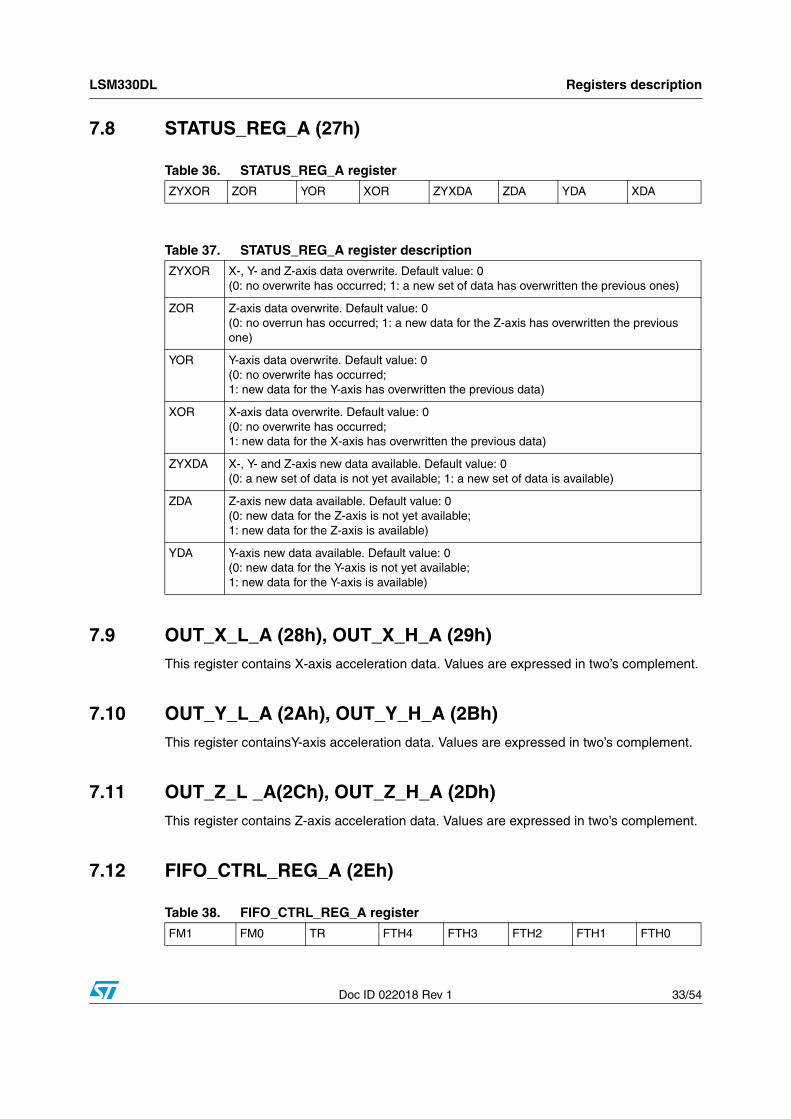
7.8 STATUS_REG_A (27h)
7.9 OUT_X_L_A (28h), OUT_X_H_A (29h)This register contains X-axis acceleration data. Values are expressed in two’s complement.
7.10 OUT_Y_L_A (2Ah), OUT_Y_H_A (2Bh)This register containsY-axis acceleration data. Values are expressed in two’s complement.
7.11 OUT_Z_L _A(2Ch), OUT_Z_H_A (2Dh)This register contains Z-axis acceleration data. Values are expressed in two’s complement.
7.12 FIFO_CTRL_REG_A (2Eh)
Table 36. STATUS_REG_A register
ZYXOR ZOR YOR XOR ZYXDA ZDA YDA XDA
Table 37. STATUS_REG_A register description
ZYXOR X-, Y- and Z-axis data overwrite. Default value: 0(0: no overwrite has occurred; 1: a new set of data has overwritten the previous ones)
ZOR Z-axis data overwrite. Default value: 0(0: no overrun has occurred; 1: a new data for the Z-axis has overwritten the previous one)
YOR Y-axis data overwrite. Default value: 0(0: no overwrite has occurred; 1: new data for the Y-axis has overwritten the previous data)
XOR X-axis data overwrite. Default value: 0(0: no overwrite has occurred; 1: new data for the X-axis has overwritten the previous data)
ZYXDA X-, Y- and Z-axis new data available. Default value: 0(0: a new set of data is not yet available; 1: a new set of data is available)
ZDA Z-axis new data available. Default value: 0(0: new data for the Z-axis is not yet available; 1: new data for the Z-axis is available)
YDA Y-axis new data available. Default value: 0(0: new data for the Y-axis is not yet available; 1: new data for the Y-axis is available)
Table 38. FIFO_CTRL_REG_A register
FM1 FM0 TR FTH4 FTH3 FTH2 FTH1 FTH0
Registers description LSM330DL
34/54 Doc ID 022018 Rev 1
7.13 FIFO_SRC_REG_A (2Fh)
7.14 INT1_CFG_A (30h)
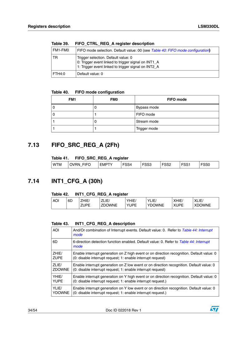
Table 39. FIFO_CTRL_REG_A register description
FM1-FM0 FIFO mode selection. Default value: 00 (see Table 40: FIFO mode configuration)
TR Trigger selection. Default value: 00: Trigger event linked to trigger signal on INT1_A 1: Trigger event linked to trigger signal on INT2_A
FTH4:0 Default value: 0
Table 40. FIFO mode configuration
FM1 FM0 FIFO mode
0 0 Bypass mode
0 1 FIFO mode
1 0 Stream mode
1 1 Trigger mode
Table 41. FIFO_SRC_REG_A register
WTM OVRN_FIFO EMPTY FSS4 FSS3 FSS2 FSS1 FSS0
Table 42. INT1_CFG_REG_A register
AOI 6D ZHIE/ZUPE
ZLIE/ZDOWNE
YHIE/YUPE
YLIE/YDOWNE
XHIE/XUPE
XLIE/XDOWNE
Table 43. INT1_CFG_REG_A description
AOI And/Or combination of Interrupt events. Default value: 0. Refer to Table 44: Interrupt mode
6D 6-direction detection function enabled. Default value: 0. Refer to Table 44: Interrupt mode
ZHIE/ZUPE
Enable interrupt generation on Z high event or on direction recognition. Default value: 0 (0: disable interrupt request; 1: enable interrupt request)
ZLIE/ZDOWNE
Enable interrupt generation on Z low event or on direction recognition. Default value: 0 (0: disable interrupt request; 1: enable interrupt request)
YHIE/YUPE
Enable interrupt generation on Y high event or on direction recognition. Default value: 0 (0: disable interrupt request; 1: enable interrupt request.)
YLIE/YDOWNE
Enable interrupt generation on Y low event or on direction recognition. Default value: 0 (0: disable interrupt request; 1: enable interrupt request.)
LSM330DL Registers description
Doc ID 022018 Rev 1 35/54
The contents of the INT1_CFG_REG_A register are loaded at boot.
A write operation at this address is possible only after system boot.
The difference between AOI-6D = ‘01’ and AOI-6D = ‘11’ is defined as follows:
AOI-6D = ‘01’ is movement recognition. An interrupt is generated when the orientation moves from an unknown zone to a known zone. The interrupt signal stays for a duration determined by ODR.
AOI-6D = ‘11’ is direction recognition. An interrupt is generated when the orientation is inside a known zone. The interrupt signal stays until orientation is inside the zone.
7.15 INT1_SRC_A (31h)
XHIE/XUPE
Enable interrupt generation on X high event or on direction recognition. Default value: 0 (0: disable interrupt request; 1: enable interrupt request.)
XLIE/XDOWNE
Enable interrupt generation on X low event or on direction recognition. Default value: 0 (0: disable interrupt request; 1: enable interrupt request.)
Table 44. Interrupt mode
AOI 6D Interrupt mode
0 0 OR combination of interrupt events
0 1 6-direction movement recognition
1 0 AND combination of interrupt events
1 1 6-direction position recognition
Table 43. INT1_CFG_REG_A description (continued)
Table 45. INT1_SRC_A register
0(1)
1. This bit has to be set to ‘0’ for correct operation.
IA ZH ZL YH YL XH XL
Table 46. INT1_SRC_A description
IAInterrupt active. Default value: 0
(0: no interrupt has been generated; 1: one or more interrupts have been generated)
ZHZ high. Default value: 0(0: no interrupt, 1: Z high event has occurred)
ZLZ low. Default value: 0(0: no interrupt; 1: Z low event has occurred)
YHY high. Default value: 0(0: no interrupt, 1: Y high event has occurred)
YLY low. Default value: 0(0: no interrupt, 1: Y low event has occurred)
Registers description LSM330DL
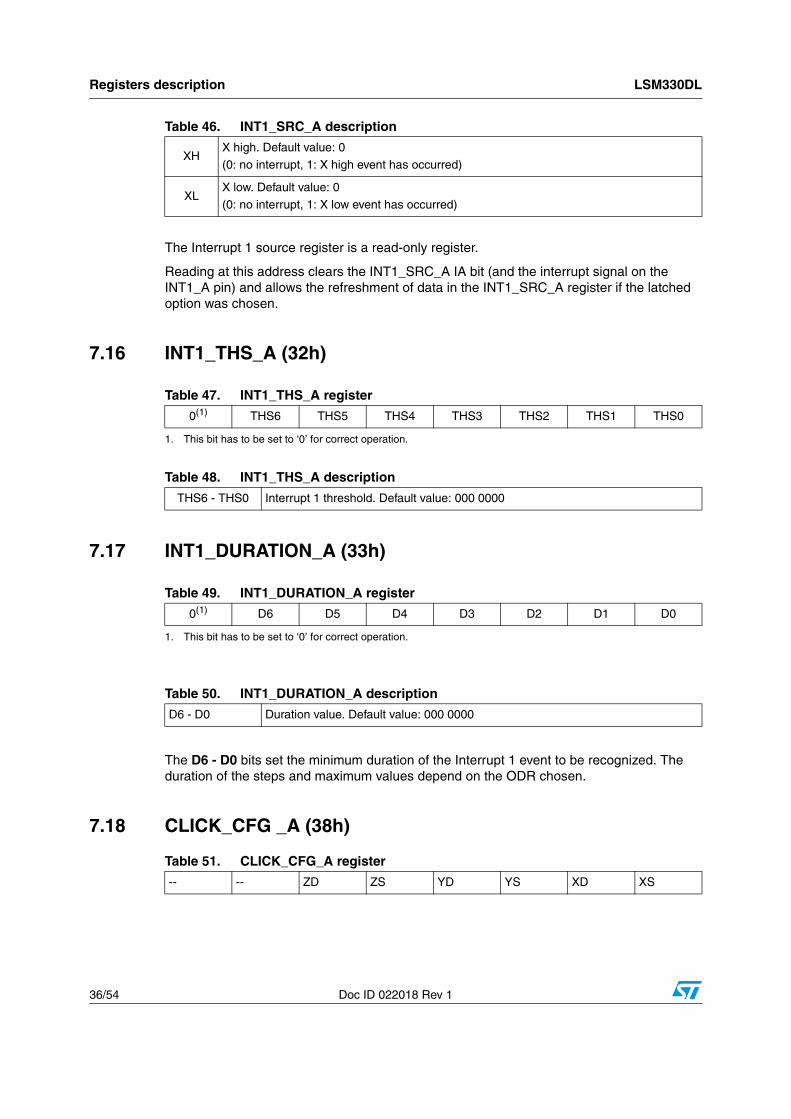
36/54 Doc ID 022018 Rev 1
The Interrupt 1 source register is a read-only register.
Reading at this address clears the INT1_SRC_A IA bit (and the interrupt signal on the INT1_A pin) and allows the refreshment of data in the INT1_SRC_A register if the latched option was chosen.
7.16 INT1_THS_A (32h)
7.17 INT1_DURATION_A (33h)
The D6 - D0 bits set the minimum duration of the Interrupt 1 event to be recognized. The duration of the steps and maximum values depend on the ODR chosen.
7.18 CLICK_CFG _A (38h)
XHX high. Default value: 0
(0: no interrupt, 1: X high event has occurred)
XLX low. Default value: 0
(0: no interrupt, 1: X low event has occurred)
Table 46. INT1_SRC_A description
Table 47. INT1_THS_A register
0(1)
1. This bit has to be set to ‘0’ for correct operation.
THS6 THS5 THS4 THS3 THS2 THS1 THS0
Table 48. INT1_THS_A description
THS6 - THS0 Interrupt 1 threshold. Default value: 000 0000
Table 49. INT1_DURATION_A register
0(1)
1. This bit has to be set to ‘0’ for correct operation.
D6 D5 D4 D3 D2 D1 D0
Table 50. INT1_DURATION_A description
D6 - D0 Duration value. Default value: 000 0000
Table 51. CLICK_CFG_A register
-- -- ZD ZS YD YS XD XS
LSM330DL Registers description
Doc ID 022018 Rev 1 37/54
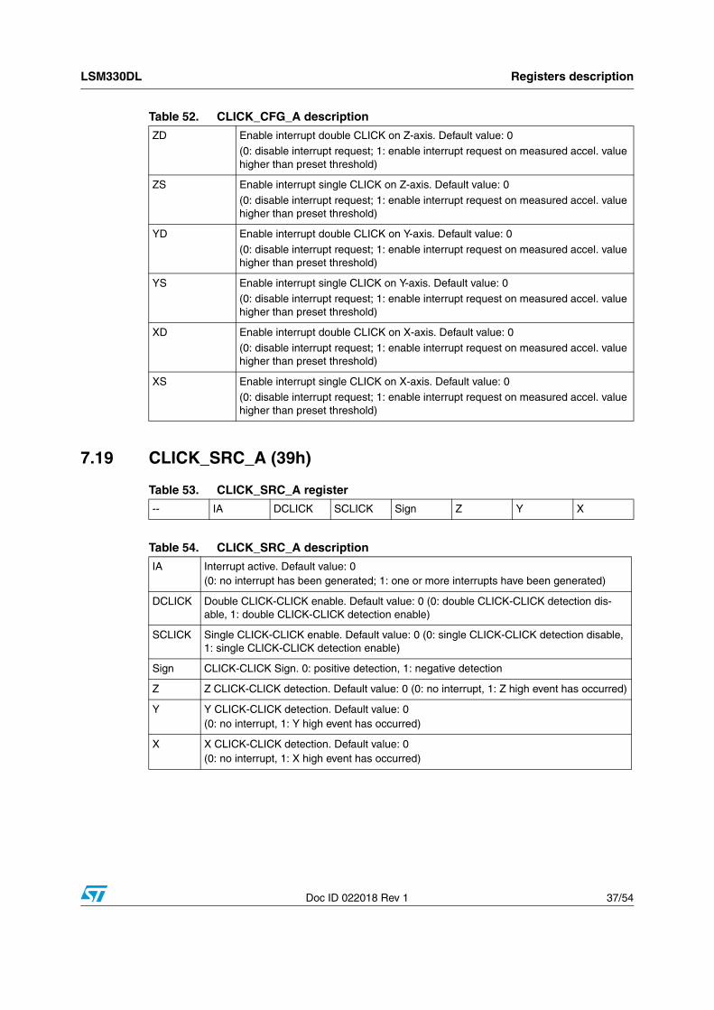
7.19 CLICK_SRC_A (39h)
Table 52. CLICK_CFG_A description
ZD Enable interrupt double CLICK on Z-axis. Default value: 0(0: disable interrupt request; 1: enable interrupt request on measured accel. value higher than preset threshold)
ZS Enable interrupt single CLICK on Z-axis. Default value: 0
(0: disable interrupt request; 1: enable interrupt request on measured accel. value higher than preset threshold)
YD Enable interrupt double CLICK on Y-axis. Default value: 0
(0: disable interrupt request; 1: enable interrupt request on measured accel. value higher than preset threshold)
YS Enable interrupt single CLICK on Y-axis. Default value: 0(0: disable interrupt request; 1: enable interrupt request on measured accel. value higher than preset threshold)
XD Enable interrupt double CLICK on X-axis. Default value: 0
(0: disable interrupt request; 1: enable interrupt request on measured accel. value higher than preset threshold)
XS Enable interrupt single CLICK on X-axis. Default value: 0(0: disable interrupt request; 1: enable interrupt request on measured accel. value higher than preset threshold)
Table 53. CLICK_SRC_A register
-- IA DCLICK SCLICK Sign Z Y X
Table 54. CLICK_SRC_A description
IA Interrupt active. Default value: 0(0: no interrupt has been generated; 1: one or more interrupts have been generated)
DCLICK Double CLICK-CLICK enable. Default value: 0 (0: double CLICK-CLICK detection dis-able, 1: double CLICK-CLICK detection enable)
SCLICK Single CLICK-CLICK enable. Default value: 0 (0: single CLICK-CLICK detection disable, 1: single CLICK-CLICK detection enable)
Sign CLICK-CLICK Sign. 0: positive detection, 1: negative detection
Z Z CLICK-CLICK detection. Default value: 0 (0: no interrupt, 1: Z high event has occurred)
Y Y CLICK-CLICK detection. Default value: 0(0: no interrupt, 1: Y high event has occurred)
X X CLICK-CLICK detection. Default value: 0(0: no interrupt, 1: X high event has occurred)
Registers description LSM330DL
38/54 Doc ID 022018 Rev 1
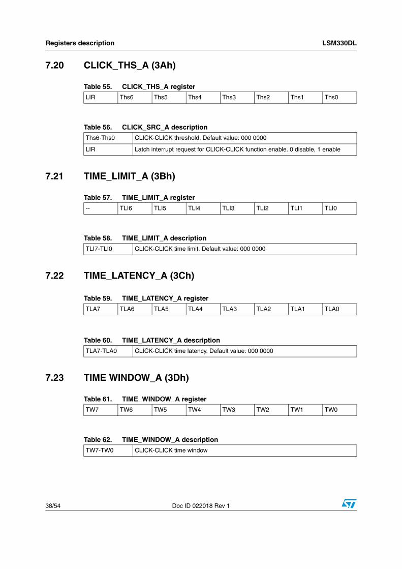
7.20 CLICK_THS_A (3Ah)
7.21 TIME_LIMIT_A (3Bh)
7.22 TIME_LATENCY_A (3Ch)
7.23 TIME WINDOW_A (3Dh)
Table 55. CLICK_THS_A register
LIR Ths6 Ths5 Ths4 Ths3 Ths2 Ths1 Ths0
Table 56. CLICK_SRC_A description
Ths6-Ths0 CLICK-CLICK threshold. Default value: 000 0000
LIR Latch interrupt request for CLICK-CLICK function enable. 0 disable, 1 enable
Table 57. TIME_LIMIT_A register
-- TLI6 TLI5 TLI4 TLI3 TLI2 TLI1 TLI0
Table 58. TIME_LIMIT_A description
TLI7-TLI0 CLICK-CLICK time limit. Default value: 000 0000
Table 59. TIME_LATENCY_A register
TLA7 TLA6 TLA5 TLA4 TLA3 TLA2 TLA1 TLA0
Table 60. TIME_LATENCY_A description
TLA7-TLA0 CLICK-CLICK time latency. Default value: 000 0000
Table 61. TIME_WINDOW_A register
TW7 TW6 TW5 TW4 TW3 TW2 TW1 TW0
Table 62. TIME_WINDOW_A description
TW7-TW0 CLICK-CLICK time window
LSM330DL Registers description
Doc ID 022018 Rev 1 39/54
7.24 CTRL_REG1_G (20h)
DR<1:0> is used to set the ODR selection. BW <1:0> is used to set bandwidth selection.
The following table gives the frequencies for all combinations of the DR / BW bits.
Table 63. CTRL_REG1_G register
DR1 DR0 BW1 BW0 PD Zen Yen Xen
Table 64. CTRL_REG1_G description
DR1-DR0 Output data rate selection. Refer to Table 65: DR and BW configuration setting
BW1-BW0 Bandwidth selection. Refer to Table 65: DR and BW configuration setting
PDPower-down mode enable. Default value: 0
(0: power-down mode, 1: normal mode or sleep mode)
Zen Z-axis enable. Default value: 1
(0: Z-axis disabled; 1: Z-axis enabled)
Yen Y-axis enable. Default value: 1
(0: Y-axis disabled; 1: Y-axis enabled)
Xen X-axis enable. Default value: 1
(0: X-axis disabled; 1: X-axis enabled)
Table 65. DR and BW configuration setting
DR <1:0> BW <1:0> ODR [Hz] cutoff [Hz]
00 00 100 12.5
00 01 100 25
00 10 100 25
00 11 100 25
01 00 200 12.5
01 01 200 25
01 10 200 50
01 11 200 70
10 00 400 20
10 01 400 25
10 10 400 50
10 11 400 110
11 00 800 30
11 01 800 35
11 10 800 50
11 11 800 110
Registers description LSM330DL
40/54 Doc ID 022018 Rev 1
Combination of PD, Zen, Yen, Xen are used to set device in different modes (power-down / normal / sleep mode) according to the following table.
7.25 CTRL_REG2_G (21h)
Table 66. Power mode selection configuration
Mode PD Zen Yen Xen
Power-down 0 - - -
Sleep 1 0 0 0
Normal 1 - - -
Table 67. CTRL_REG2_G register
0(1)
1. This bit has to be set to ‘0’ for correct operation.
0(1) HPM1 HPM1 HPCF3 HPCF2 HPCF1 HPCF0
Table 68. CTRL_REG2_G description
HPM1-HPM0
High-pass filter mode selection. Default value: 00Refer to Table 69: High-pass filter mode configuration
HPCF3-HPCF0
High-pass filter cutoff frequency selectionRefer to Table 70: High-pass filter cutoff frequency configuration [Hz]
Table 69. High-pass filter mode configuration
HPM1 HPM0 High-pass filter mode
0 0 Normal mode (reset reading HP_RESET_FILTER)
0 1 Reference signal for filtering
1 0 Normal mode
1 1 Autoreset on interrupt event
Table 70. High-pass filter cutoff frequency configuration [Hz]
HPCF3-0 ODR = 100 Hz ODR = 200 Hz ODR = 400 Hz ODR = 800 Hz
0000 8 15 30 56
0001 4 8 15 30
0010 2 4 8 15
0011 1 2 4 8
0100 0.5 1 2 4
0101 0.2 0.5 1 2
LSM330DL Registers description
Doc ID 022018 Rev 1 41/54
7.26 CTRL_REG3_G (22h)
7.27 CTRL_REG4_G (23h)
0110 0.1 0.2 0.5 1
0111 0.05 0.1 0.2 0.5
1000 0.02 0.05 0.1 0.2
1001 0.01 0.02 0.05 0.1
Table 70. High-pass filter cutoff frequency configuration [Hz] (continued)
HPCF3-0 ODR = 100 Hz ODR = 200 Hz ODR = 400 Hz ODR = 800 Hz
Table 71. CTRL_REG3_G register
I1_Int1 I1_Boot H_Lactive PP_OD I2_DRDY I2_WTM I2_ORun I2_Empty
Table 72. CTRL_REG3_G description
I1_Int1 Interrupt enable on INT1_G pin. Default value 0. (0: Disable; 1: Enable)
I1_Boot Boot status available on INT1_G. Default value 0. (0: Disable; 1: Enable)
H_Lactive Interrupt active configuration on INT1_G. Default value 0. (0: High; 1:Low)
PP_OD Push-Pull / Open drain. Default value: 0. (0: Push-Pull; 1: Open drain)
I2_DRDY Date Ready on DRDY_G/INT2_G. Default value 0. (0: Disable; 1: Enable)
I2_WTM FIFO watermark interrupt on DRDY_G/INT2_G. Default value: 0. (0: Disable; 1: Enable)
I2_ORun FIFO overrun interrupt on DRDY_G/INT2_G Default value: 0. (0: Disable; 1: Enable)
I2_Empty FIFO empty interrupt on DRDY_G/INT2_G. Default value: 0. (0: Disable; 1: Enable)
Table 73. CTRL_REG4_G register
BDU BLE FS1 FS0 -- 0(1)
1. This bit has to be set to ‘0’ for correct operation.
0(1) SIM
Table 74. CTRL_REG4_G description
BDU Block data update. Default value: 0(0: continuous update; 1: output registers not updated until MSB and LSB have been read)
BLE Big/little endian data selection. Default value 0.(0: Data LSB at lower address; 1: Data MSB at lower address)
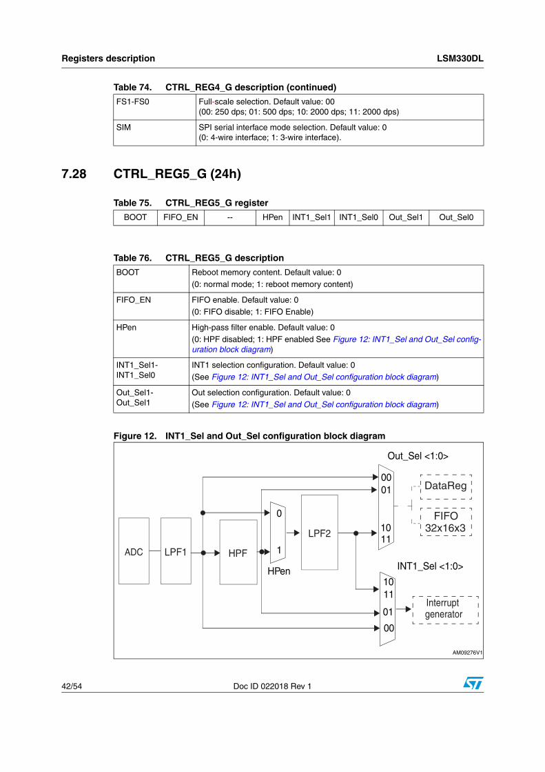
Registers description LSM330DL
42/54 Doc ID 022018 Rev 1
7.28 CTRL_REG5_G (24h)
Figure 12. INT1_Sel and Out_Sel configuration block diagram
FS1-FS0 Full-scale selection. Default value: 00(00: 250 dps; 01: 500 dps; 10: 2000 dps; 11: 2000 dps)
SIM SPI serial interface mode selection. Default value: 0 (0: 4-wire interface; 1: 3-wire interface).
Table 74. CTRL_REG4_G description (continued)
Table 75. CTRL_REG5_G register
BOOT FIFO_EN -- HPen INT1_Sel1 INT1_Sel0 Out_Sel1 Out_Sel0
Table 76. CTRL_REG5_G description
BOOT Reboot memory content. Default value: 0
(0: normal mode; 1: reboot memory content)
FIFO_EN FIFO enable. Default value: 0(0: FIFO disable; 1: FIFO Enable)
HPen High-pass filter enable. Default value: 0(0: HPF disabled; 1: HPF enabled See Figure 12: INT1_Sel and Out_Sel config-uration block diagram)
INT1_Sel1-INT1_Sel0
INT1 selection configuration. Default value: 0
(See Figure 12: INT1_Sel and Out_Sel configuration block diagram)
Out_Sel1-Out_Sel1
Out selection configuration. Default value: 0
(See Figure 12: INT1_Sel and Out_Sel configuration block diagram)
ADC LPF1 HPF
0
1
HPen
LPF2 10 11
01 00
Out_Sel <1:0>
DataReg
FIFO 32x16x3
00
11 10
01 Interrupt generator
INT1_Sel <1:0>
AM09276V1
LSM330DL Registers description
Doc ID 022018 Rev 1 43/54
7.29 REFERENCE/DATACAPTURE_G (25h)
7.30 OUT_TEMP_G (26h)
Table 77. Out_Sel configuration setting
Hpen OUT_SEL1 OUT_SEL0 Description
x 0 0Data in DataReg and FIFO are non-high-pass-filtered
x 0 1Data in DataReg and FIFO are high-pass-filtered
0 1 xData in DataReg and FIFO are low-pass-filtered by LPF2
1 1 xData in DataReg and FIFO are high-pass and low-pass-filtered by LPF2
Table 78. INT_SEL configuration setting
Hpen INT_SEL1 INT_SEL2 Description
x 0 0Non-high-pass-filtered data are used for interrupt generation
x 0 1High-pass-filtered data are used for interrupt generation
0 1 xLow-pass-filtered data are used for interrupt generation
1 1 xHigh-pass and low-pass-filtered data are used for interrupt generation
Table 79. REFERENCE/DATACAPTURE_G register
Ref7 Ref6 Ref5 Ref4 Ref3 Ref2 Ref1 Ref0
Table 80. REFERENCE/DATACAPTURE_G register description
Ref 7-Ref0 Reference value for interrupt generation. Default value: 0
Table 81. OUT_TEMP_G register
Temp7 Temp6 Temp5 Temp4 Temp3 Temp2 Temp1 Temp0
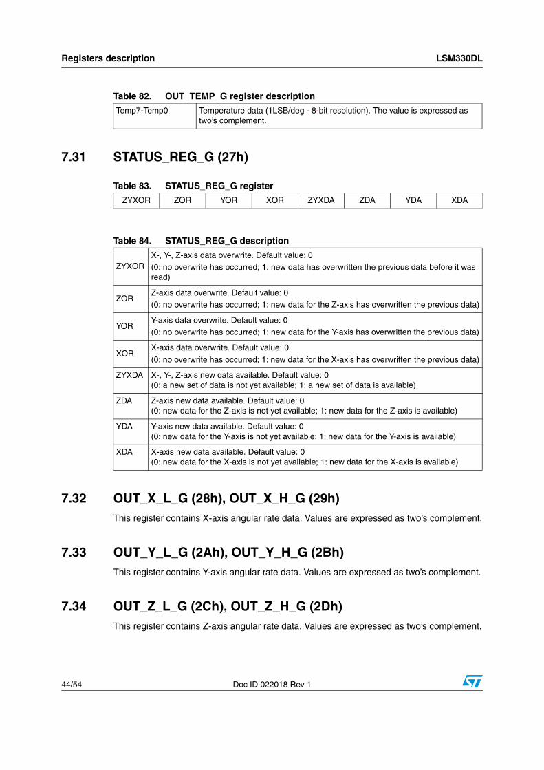
Registers description LSM330DL
44/54 Doc ID 022018 Rev 1
7.31 STATUS_REG_G (27h)
7.32 OUT_X_L_G (28h), OUT_X_H_G (29h)This register contains X-axis angular rate data. Values are expressed as two’s complement.
7.33 OUT_Y_L_G (2Ah), OUT_Y_H_G (2Bh)This register contains Y-axis angular rate data. Values are expressed as two’s complement.
7.34 OUT_Z_L_G (2Ch), OUT_Z_H_G (2Dh)This register contains Z-axis angular rate data. Values are expressed as two’s complement.
Table 82. OUT_TEMP_G register description
Temp7-Temp0 Temperature data (1LSB/deg - 8-bit resolution). The value is expressed as two’s complement.
Table 83. STATUS_REG_G register
ZYXOR ZOR YOR XOR ZYXDA ZDA YDA XDA
Table 84. STATUS_REG_G description
ZYXORX-, Y-, Z-axis data overwrite. Default value: 0
(0: no overwrite has occurred; 1: new data has overwritten the previous data before it was read)
ZORZ-axis data overwrite. Default value: 0
(0: no overwrite has occurred; 1: new data for the Z-axis has overwritten the previous data)
YORY-axis data overwrite. Default value: 0
(0: no overwrite has occurred; 1: new data for the Y-axis has overwritten the previous data)
XORX-axis data overwrite. Default value: 0
(0: no overwrite has occurred; 1: new data for the X-axis has overwritten the previous data)
ZYXDA X-, Y-, Z-axis new data available. Default value: 0(0: a new set of data is not yet available; 1: a new set of data is available)
ZDA Z-axis new data available. Default value: 0(0: new data for the Z-axis is not yet available; 1: new data for the Z-axis is available)
YDA Y-axis new data available. Default value: 0(0: new data for the Y-axis is not yet available; 1: new data for the Y-axis is available)
XDA X-axis new data available. Default value: 0(0: new data for the X-axis is not yet available; 1: new data for the X-axis is available)
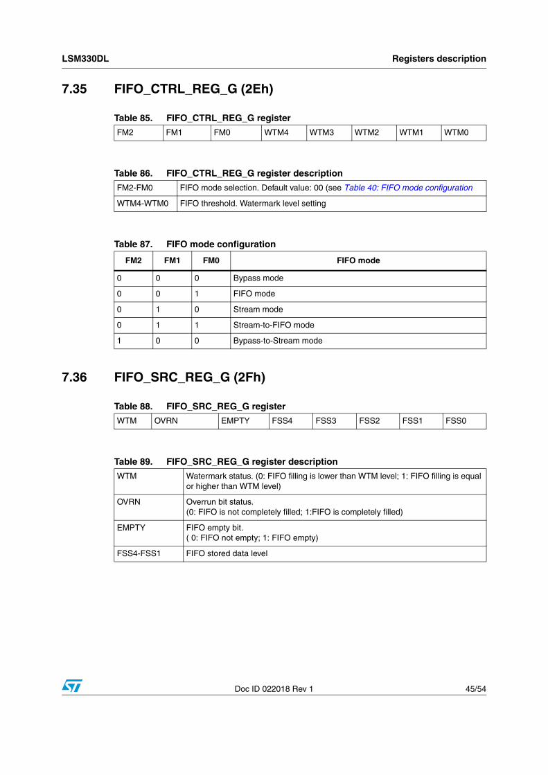
LSM330DL Registers description
Doc ID 022018 Rev 1 45/54
7.35 FIFO_CTRL_REG_G (2Eh)
7.36 FIFO_SRC_REG_G (2Fh)
Table 85. FIFO_CTRL_REG_G register
FM2 FM1 FM0 WTM4 WTM3 WTM2 WTM1 WTM0
Table 86. FIFO_CTRL_REG_G register description
FM2-FM0 FIFO mode selection. Default value: 00 (see Table 40: FIFO mode configuration
WTM4-WTM0 FIFO threshold. Watermark level setting
Table 87. FIFO mode configuration
FM2 FM1 FM0 FIFO mode
0 0 0 Bypass mode
0 0 1 FIFO mode
0 1 0 Stream mode
0 1 1 Stream-to-FIFO mode
1 0 0 Bypass-to-Stream mode
Table 88. FIFO_SRC_REG_G register
WTM OVRN EMPTY FSS4 FSS3 FSS2 FSS1 FSS0
Table 89. FIFO_SRC_REG_G register description
WTM Watermark status. (0: FIFO filling is lower than WTM level; 1: FIFO filling is equal or higher than WTM level)
OVRN Overrun bit status. (0: FIFO is not completely filled; 1:FIFO is completely filled)
EMPTY FIFO empty bit. ( 0: FIFO not empty; 1: FIFO empty)
FSS4-FSS1 FIFO stored data level
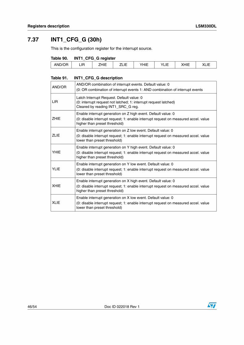
Registers description LSM330DL
46/54 Doc ID 022018 Rev 1
7.37 INT1_CFG_G (30h)This is the configuration register for the interrupt source.
Table 90. INT1_CFG_G register
AND/OR LIR ZHIE ZLIE YHIE YLIE XHIE XLIE
Table 91. INT1_CFG_G description
AND/ORAND/OR combination of interrupt events. Default value: 0(0: OR combination of interrupt events 1: AND combination of interrupt events
LIRLatch Interrupt Request. Default value: 0(0: interrupt request not latched; 1: interrupt request latched)Cleared by reading INT1_SRC_G reg.
ZHIEEnable interrupt generation on Z high event. Default value: 0(0: disable interrupt request; 1: enable interrupt request on measured accel. value higher than preset threshold)
ZLIEEnable interrupt generation on Z low event. Default value: 0
(0: disable interrupt request; 1: enable interrupt request on measured accel. value lower than preset threshold)
YHIEEnable interrupt generation on Y high event. Default value: 0
(0: disable interrupt request; 1: enable interrupt request on measured accel. value higher than preset threshold)
YLIEEnable interrupt generation on Y low event. Default value: 0(0: disable interrupt request; 1: enable interrupt request on measured accel. value lower than preset threshold)
XHIEEnable interrupt generation on X high event. Default value: 0
(0: disable interrupt request; 1: enable interrupt request on measured accel. value higher than preset threshold)
XLIEEnable interrupt generation on X low event. Default value: 0
(0: disable interrupt request; 1: enable interrupt request on measured accel. value lower than preset threshold)
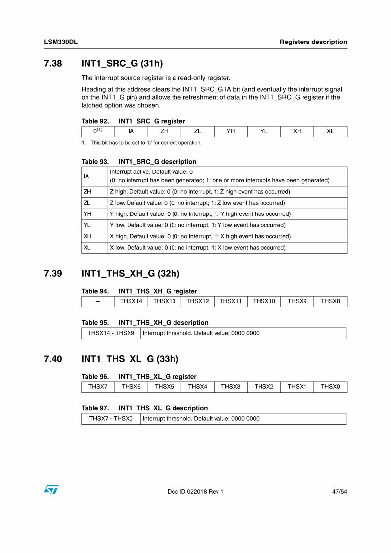
LSM330DL Registers description
Doc ID 022018 Rev 1 47/54
7.38 INT1_SRC_G (31h)The interrupt source register is a read-only register.
Reading at this address clears the INT1_SRC_G IA bit (and eventually the interrupt signal on the INT1_G pin) and allows the refreshment of data in the INT1_SRC_G register if the latched option was chosen.
7.39 INT1_THS_XH_G (32h)
7.40 INT1_THS_XL_G (33h)
Table 92. INT1_SRC_G register
0(1)
1. This bit has to be set to ‘0’ for correct operation.
IA ZH ZL YH YL XH XL
Table 93. INT1_SRC_G description
IAInterrupt active. Default value: 0 (0: no interrupt has been generated; 1: one or more interrupts have been generated)
ZH Z high. Default value: 0 (0: no interrupt, 1: Z high event has occurred)
ZL Z low. Default value: 0 (0: no interrupt; 1: Z low event has occurred)
YH Y high. Default value: 0 (0: no interrupt, 1: Y high event has occurred)
YL Y low. Default value: 0 (0: no interrupt, 1: Y low event has occurred)
XH X high. Default value: 0 (0: no interrupt, 1: X high event has occurred)
XL X low. Default value: 0 (0: no interrupt, 1: X low event has occurred)
Table 94. INT1_THS_XH_G register
-- THSX14 THSX13 THSX12 THSX11 THSX10 THSX9 THSX8
Table 95. INT1_THS_XH_G description
THSX14 - THSX9 Interrupt threshold. Default value: 0000 0000
Table 96. INT1_THS_XL_G register
THSX7 THSX6 THSX5 THSX4 THSX3 THSX2 THSX1 THSX0
Table 97. INT1_THS_XL_G description
THSX7 - THSX0 Interrupt threshold. Default value: 0000 0000
Registers description LSM330DL
48/54 Doc ID 022018 Rev 1
7.41 INT1_THS_YH_G (34h)
7.42 INT1_THS_YL_G (35h)
7.43 INT1_THS_ZH_G (36h)
7.44 INT1_THS_ZL_G (37h)
Table 98. INT1_THS_YH_G register
-- THSY14 THSY13 THSY12 THSY11 THSY10 THSY9 THSY8
Table 99. INT1_THS_YH_G description
THSY14 - THSY9 Interrupt threshold. Default value: 0000 0000
Table 100. INT1_THS_YL_G register
THSR7 THSY6 THSY5 THSY4 THSY3 THSY2 THSY1 THSY0
Table 101. INT1_THS_YL_G description
THSY7 - THSY0 Interrupt threshold. Default value: 0000 0000
Table 102. INT1_THS_ZH_G register
-- THSZ14 THSZ13 THSZ12 THSZ11 THSZ10 THSZ9 THSZ8
Table 103. INT1_THS_ZH_G description
THSZ14 - THSZ9 Interrupt threshold. Default value: 0000 0000
Table 104. INT1_THS_ZL_G register
THSZ7 THSZ6 THSZ5 THSZ4 THSZ3 THSZ2 THSZ1 THSZ0
Table 105. INT1_THS_ZL_G description
THSZ7 - THSZ0 Interrupt threshold. Default value: 0000 0000
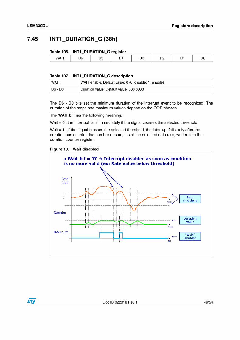
LSM330DL Registers description
Doc ID 022018 Rev 1 49/54
7.45 INT1_DURATION_G (38h)
The D6 - D0 bits set the minimum duration of the interrupt event to be recognized. Theduration of the steps and maximum values depend on the ODR chosen.
The WAIT bit has the following meaning:
Wait =’0’: the interrupt falls immediately if the signal crosses the selected threshold
Wait =’1’: if the signal crosses the selected threshold, the interrupt falls only after the duration has counted the number of samples at the selected data rate, written into the duration counter register.
Figure 13. Wait disabled
Table 106. INT1_DURATION_G register
WAIT D6 D5 D4 D3 D2 D1 D0
Table 107. INT1_DURATION_G description
WAIT WAIT enable. Default value: 0 (0: disable; 1: enable)
D6 - D0 Duration value. Default value: 000 0000
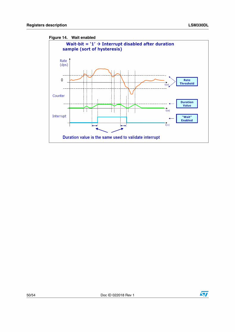
Registers description LSM330DL
50/54 Doc ID 022018 Rev 1
Figure 14. Wait enabled
LSM330DL Package information
Doc ID 022018 Rev 1 51/54
8 Package information
In order to meet environmental requirements, ST offers these devices in different grades ofECOPACK® packages, depending on their level of environmental compliance. ECOPACK®
specifications, grade definitions and product status are available at: www.st.com. ECOPACKis an ST trademark.
ECOPACK® specifications are available at: www.st.com.
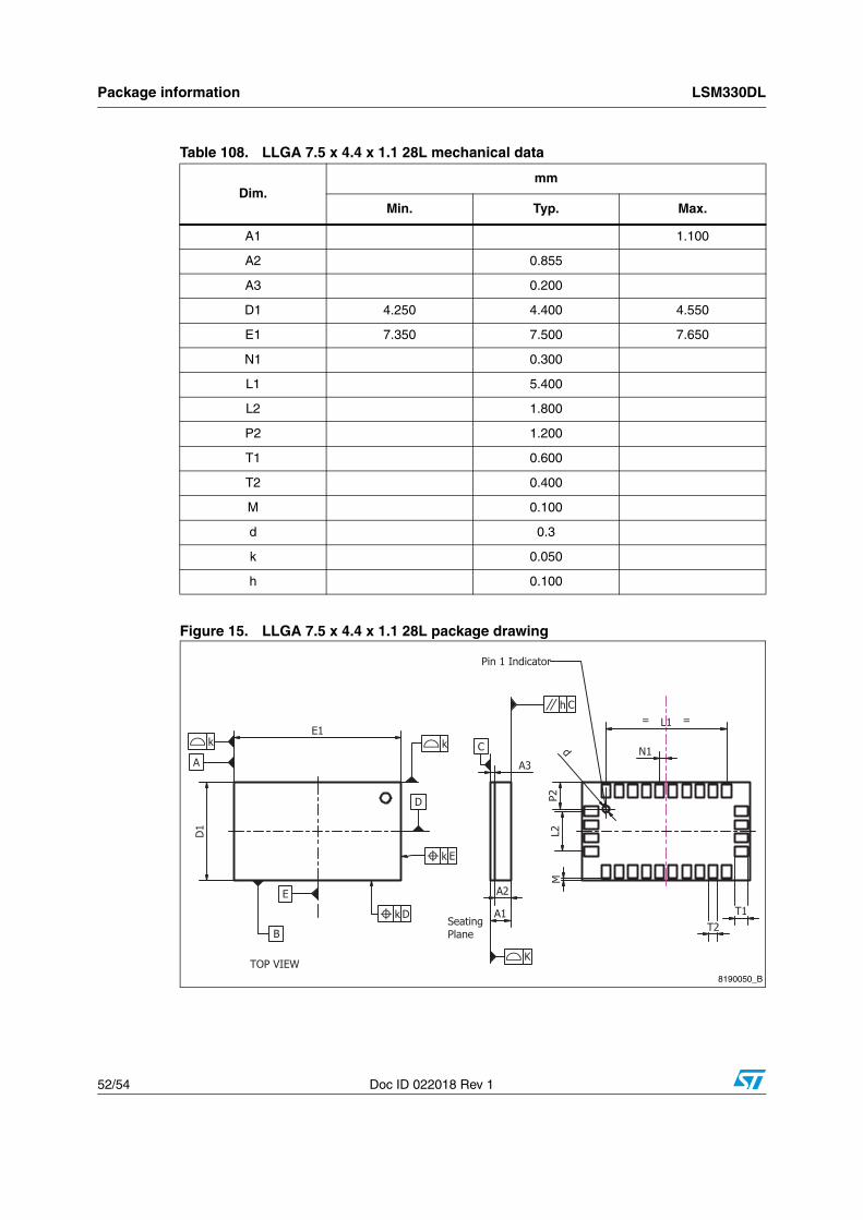
Package information LSM330DL
52/54 Doc ID 022018 Rev 1
Figure 15. LLGA 7.5 x 4.4 x 1.1 28L package drawing
Table 108. LLGA 7.5 x 4.4 x 1.1 28L mechanical data
Dim. mm
Min. Typ. Max.
A1 1.100
A2 0.855
A3 0.200
D1 4.250 4.400 4.550
E1 7.350 7.500 7.650
N1 0.300
L1 5.400
L2 1.800
P2 1.200
T1 0.600
T2 0.400
M 0.100
d 0.3
k 0.050
h 0.100
D1
E1
A1
P2
L1
T2T1
L2
d
M
B
E
D
A
k
k D
k E
K
h C
C
Pin 1 Indicator
TOP VIEW
Seating Plane
N1
= =
A3
A2
k
8190050_B
LSM330DL Revision history
Doc ID 022018 Rev 1 53/54
9 Revision history
Table 109. Document revision history
Date Revision Changes
19-Jul-2011 1 First release.
LSM330DL
54/54 Doc ID 022018 Rev 1
Please Read Carefully:
Information in this document is provided solely in connection with ST products. STMicroelectronics NV and its subsidiaries (“ST”) reserve theright to make changes, corrections, modifications or improvements, to this document, and the products and services described herein at anytime, without notice.
All ST products are sold pursuant to ST’s terms and conditions of sale.
Purchasers are solely responsible for the choice, selection and use of the ST products and services described herein, and ST assumes noliability whatsoever relating to the choice, selection or use of the ST products and services described herein.
No license, express or implied, by estoppel or otherwise, to any intellectual property rights is granted under this document. If any part of thisdocument refers to any third party products or services it shall not be deemed a license grant by ST for the use of such third party productsor services, or any intellectual property contained therein or considered as a warranty covering the use in any manner whatsoever of suchthird party products or services or any intellectual property contained therein.
UNLESS OTHERWISE SET FORTH IN ST’S TERMS AND CONDITIONS OF SALE ST DISCLAIMS ANY EXPRESS OR IMPLIEDWARRANTY WITH RESPECT TO THE USE AND/OR SALE OF ST PRODUCTS INCLUDING WITHOUT LIMITATION IMPLIEDWARRANTIES OF MERCHANTABILITY, FITNESS FOR A PARTICULAR PURPOSE (AND THEIR EQUIVALENTS UNDER THE LAWSOF ANY JURISDICTION), OR INFRINGEMENT OF ANY PATENT, COPYRIGHT OR OTHER INTELLECTUAL PROPERTY RIGHT.
UNLESS EXPRESSLY APPROVED IN WRITING BY AN AUTHORIZED ST REPRESENTATIVE, ST PRODUCTS ARE NOTRECOMMENDED, AUTHORIZED OR WARRANTED FOR USE IN MILITARY, AIR CRAFT, SPACE, LIFE SAVING, OR LIFE SUSTAININGAPPLICATIONS, NOR IN PRODUCTS OR SYSTEMS WHERE FAILURE OR MALFUNCTION MAY RESULT IN PERSONAL INJURY,DEATH, OR SEVERE PROPERTY OR ENVIRONMENTAL DAMAGE. ST PRODUCTS WHICH ARE NOT SPECIFIED AS "AUTOMOTIVEGRADE" MAY ONLY BE USED IN AUTOMOTIVE APPLICATIONS AT USER’S OWN RISK.
Resale of ST products with provisions different from the statements and/or technical features set forth in this document shall immediately voidany warranty granted by ST for the ST product or service described herein and shall not create or extend in any manner whatsoever, anyliability of ST.
ST and the ST logo are trademarks or registered trademarks of ST in various countries.
Information in this document supersedes and replaces all information previously supplied.
The ST logo is a registered trademark of STMicroelectronics. All other names are the property of their respective owners.
© 2011 STMicroelectronics - All rights reserved
STMicroelectronics group of companies
Australia - Belgium - Brazil - Canada - China - Czech Republic - Finland - France - Germany - Hong Kong - India - Israel - Italy - Japan - Malaysia - Malta - Morocco - Philippines - Singapore - Spain - Sweden - Switzerland - United Kingdom - United States of America
www.st.com