data sheetunisemicon.com.cn/upfile/2020623923315471.pdf · uniic_techdoc, rev. 4c 2019-07 / 23 data...
TRANSCRIPT
Jul. 2019
SCQ08GS03H1F1C-26V
260-Pin Unbuffered Small Outline DDR4 SDRAM
M odules EU RoHS Compliant
Data Sheet
Rev. C
UniIC_Techdoc, Rev. C 2019-07 2 / 23
Data Sheet
SCQ08GS03H1F1C-26V
Unbuffered Small Outline DDR4 SDRAM Module
Revision History
Date Revision Subjects (major changes since last revision)
2019-02 A Initial Release
2019-06 B Modify Package Dimensions
2019-07 C Modify Package Dimensions
Format Review (2020-05)
We Listen to Your Comments
Any information within this document that you feel is wrong, unclear or missing at all? Your feedback will help us to
continuously improve the quality of this document. Please send your proposal (including a reference to this document) to:
UniIC_Techdoc, Rev. C 2019-07 3 / 23
Data Sheet
SCQ08GS03H1F1C-26V
Unbuffered Small Outline DDR4 SDRAM Module
Contents
Contents ........................................................................................................................................................................................ 3
1 Overview ............................................................................................................................................................................... 4
1.1 Features ....................................................................................................................................................................... 4
1.2 Description ................................................................................................................................................................... 5
2 Pin Configurations ................................................................................................................................................................. 6
2.1 Pin Configurations ........................................................................................................................................................ 6
2.2 Pin Description ............................................................................................................................................................. 8
3 General Description ............................................................................................................................................................ 10
3.1 General Description .................................................................................................................................................... 10
3.2 Serial Presence-Detect EEPROM Operation ............................................................................................................. 10
3.3 Function Block Diagram ............................................................................................................................................. 11
3.4 DQ Map ...................................................................................................................................................................... 12
4 Electrical Characteristics ..................................................................................................................................................... 13
4.1 Absolute Maximum Ratings ........................................................................................................................................ 13
4.2 Operating Conditions .................................................................................................................................................. 14
4.3 Module and Component Speed Grades ..................................................................................................................... 15
4.4 IDD Specifications and Conditions ............................................................................................................................. 16
5 Package Dimensions .......................................................................................................................................................... 20
List of Figures .............................................................................................................................................................................. 21
List of Tables ............................................................................................................................................................................... 22
UniIC_Techdoc, Rev. C 2019-07 4 / 23
Data Sheet
SCQ08GS03H1F1C-26V
Unbuffered Small Outline DDR4 SDRAM Module
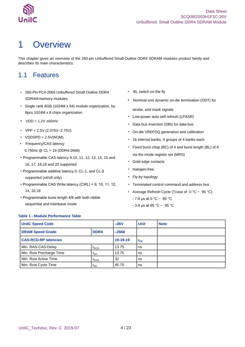
1 Overview
This chapter gives an overview of the 260-pin Unbuffered Small Outline DDR4 SDRAM modules product family and
describes its main characteristics.
1.1 Features
• 260-Pin PC4-2666 Unbuffered Small Outline DDR4
SDRAM memory modules.
• Single rank 8GB (1024M x 64) module organization, by
8pcs 1024M x 8 chips organization.
• VDD = 1.2V ±60mV
• VPP = 2.5V (2.375V~2.75V)
• VDDSPD = 2.5V(NOM)
• Frequency/CAS latency
0.750ns @ CL = 19 (DDR4-2666)
• Programmable CAS latency 9,10, 11, 12, 13, 14, 15 and
16, 17, 18,19 and 20 supported
• Programmable additive latency 0, CL-1, and CL-
supported (x4/x8 only)
• Programmable CAS Write latency (CWL) = 9, 10, 11, 12,
14, 16,18
• Programmable burst length 4/8 with both nibble
sequential and interleave mode
• BL switch on the fly
• Nominal and dynamic on-die termination (ODT) for
strobe, and mask signals
• Low-power auto self refresh (LPASR)
• Data bus inversion (DBI) for data bus
• On-die VREFDQ generation and calibration
• 16 internal banks; 4 groups of 4 banks each
• Fixed burst chop (BC) of 4 and burst length (BL) of 8
via the mode register set (MRS)
• Gold edge contacts
• Halogen-free
• Fly-by topology
• Terminated control command and address bus
• Average Refresh Cycle (Tcase of 0 °C ~ 95 °C)
- 7.8 μs at 0 °C ~ 85 °C
- 3.9 μs at 85 °C ~ 95 °C
Table 1 - Module Performance Table
UniIC Speed Code –26V Unit Note
DRAM Speed Grade DDR4 –2666
CAS-RCD-RP latencies 19-19-19 tCK
Min. RAS-CAS-Delay tRCD 13.75 ns Min. Row Precharge Time tRP 13.75 ns Min. Row Active Time tRAS 32 ns Min. Row Cycle Time tRC 45.75 ns
UniIC_Techdoc, Rev. C 2019-07 5 / 23
Data Sheet
SCQ08GS03H1F1C-26V
Unbuffered Small Outline DDR4 SDRAM Module
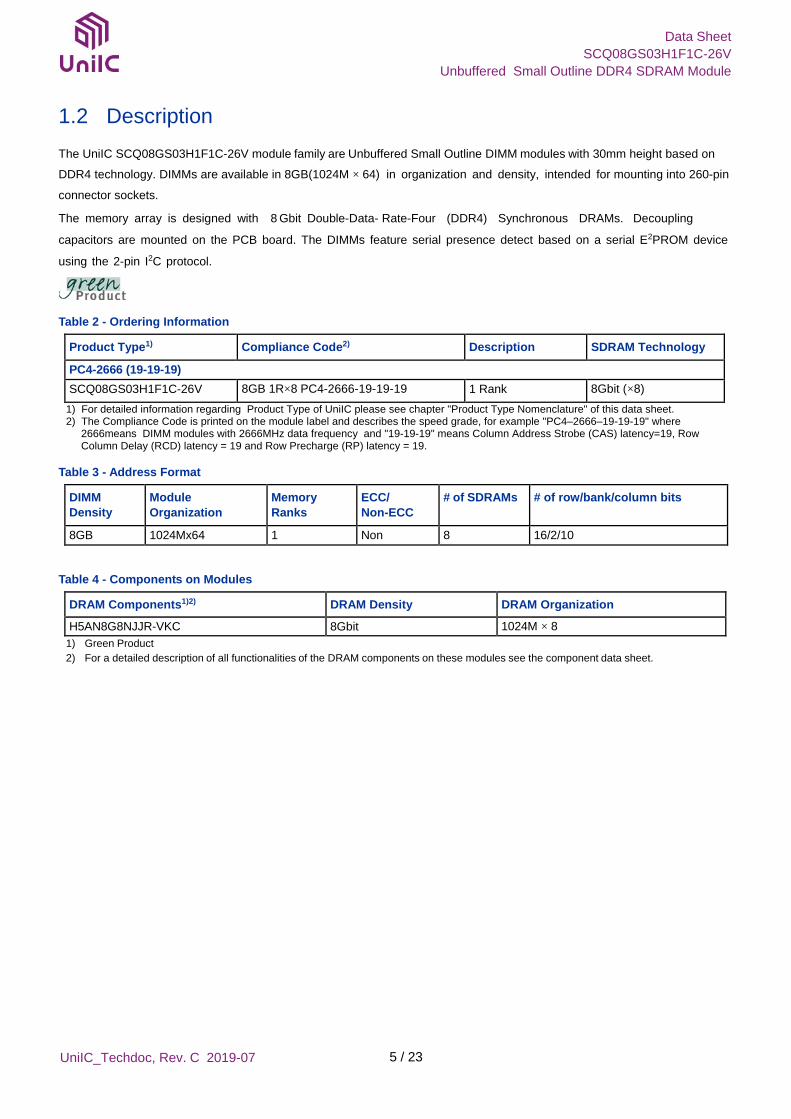
1.2 Description
The UniIC SCQ08GS03H1F1C-26V module family are Unbuffered Small Outline DIMM modules with 30mm height based on
DDR4 technology. DIMMs are available in 8GB(1024M × 64) in organization and density, intended for mounting into 260-pin
connector sockets.
The memory array is designed with 8 Gbit Double-Data- Rate-Four (DDR4) Synchronous DRAMs. Decoupling
capacitors are mounted on the PCB board. The DIMMs feature serial presence detect based on a serial E2PROM device
using the 2-pin I2C protocol.
Table 2 - Ordering Information
Product Type1) Compliance Code2) Description SDRAM Technology
PC4-2666 (19-19-19)
SCQ08GS03H1F1C-26V 8GB 1R×8 PC4-2666-19-19-19 1 Rank 8Gbit (×8)
1) For detailed information regarding Product Type of UniIC please see chapter "Product Type Nomenclature" of this data sheet. 2) The Compliance Code is printed on the module label and describes the speed grade, for example "PC4–2666–19-19-19" where
2666means DIMM modules with 2666MHz data frequency and "19-19-19" means Column Address Strobe (CAS) latency=19, Row Column Delay (RCD) latency = 19 and Row Precharge (RP) latency = 19.
Table 3 - Address Format
DIMM
Density Module
Organization Memory
Ranks ECC/
Non-ECC # of SDRAMs # of row/bank/column bits
8GB 1024Mx64 1 Non 8 16/2/10
Table 4 - Components on Modules
DRAM Components1)2) DRAM Density DRAM Organization
H5AN8G8NJJR-VKC 8Gbit 1024M × 8 1) Green Product
2) For a detailed description of all functionalities of the DRAM components on these modules see the component data sheet.
UniIC_Techdoc, Rev. C 2019-07 6 / 23
Data Sheet
SCQ08GS03H1F1C-26V
Unbuffered Small Outline DDR4 SDRAM Module
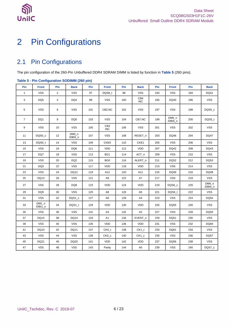
2 Pin Configurations
2.1 Pin Configurations
The pin configuration of the 260-Pin Unbuffered DDR4 SDRAM DIMM is listed by function in Table 5 (260 pins).
Table 5 - Pin Configuration SODIMM (260 pin)
Pin Front Pin Back Pin Front Pin Back Pin Front Pin Back
1 VSS 2 VSS 97 DQS8_t 98 VSS 193 VSS 194 DQ41
3 DQ5 4 DQ4 99 VSS 100 CB6 /NC
195 DQ40 196 VSS
5 VSS 6 VSS 101 CB2,NC 102 VSS 197 VSS 198 DQS5_c
7 DQ1 8 DQ0 103 VSS 104 CB7,NC 199 DM5_n /DBI5_n
200 DQS5_t
9 VSS 10 VSS 105 CB3 /NC
106 VSS 201 VSS 202 VSS
11 DQS0_c 12 DM0_n /DBI0_n
107 VSS 108 RESET_n 203 DQ46 204 DQ47
13 DQS0_t 14 VSS 109 CKE0 110 CKE1 205 VSS 206 VSS
15 VSS 16 DQ6 111 VDD 112 VDD 207 DQ42 208 DQ43
17 DQ7 18 VSS 113 BG1 114 ACT_n 209 VSS 210 VSS
19 VSS 20 DQ2 115 BG0 116 ALERT_n 211 DQ52 212 DQ53
21 DQ3 22 VSS 117 VDD 118 VDD 213 VSS 214 VSS
23 VSS 24 DQ12 119 A12 120 A11 215 DQ49 216 DQ48
25 DQ13 26 VSS 121 A9 122 A7 217 VSS 218 VSS
27 VSS 28 DQ8 123 VDD 124 VDD 219 DQS6_c 220 DM6_n /DBI6_n
29 DQ9 30 VSS 125 A8 126 A5 221 DQS6_t 222 VSS
31 VSS 32 DQS1_c 127 A6 128 A4 223 VSS 224 DQ54
33 DM1_n /DBI1_n
34 DQS1_t 129 VDD 130 VDD 225 DQ55 226 VSS
35 VSS 36 VSS 131 A3 132 A2 227 VSS 228 DQ50
37 DQ15 38 DQ14 133 A1 134 EVENT_n 229 DQ51 230 VSS
39 VSS 40 VSS 135 VDD 136 VDD 231 VSS 232 DQ60
41 DQ10 42 DQ11 137 CK0_t 138 CK1_t 233 DQ61 234 VSS
43 VSS 44 VSS 139 CK0_c 140 CK1_c 235 VSS 236 DQ57
45 DQ21 46 DQ20 141 VDD 142 VDD 237 DQ56 238 VSS
47 VSS 48 VSS 143 Parity 144 A0 239 VSS 240 DQS7_c
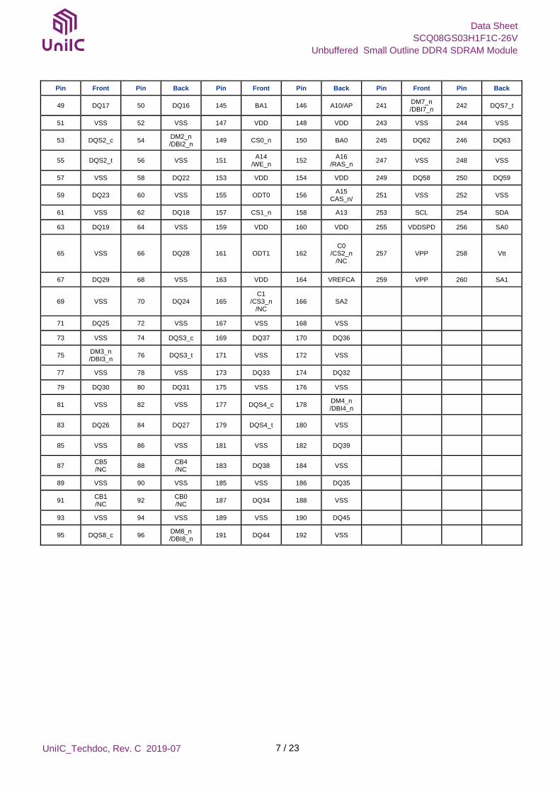
UniIC_Techdoc, Rev. C 2019-07 7 / 23
Data Sheet
SCQ08GS03H1F1C-26V
Unbuffered Small Outline DDR4 SDRAM Module
Pin Front Pin Back Pin Front Pin Back Pin Front Pin Back
49 DQ17 50 DQ16 145 BA1 146 A10/AP 241 DM7_n /DBI7_n
242 DQS7_t
51 VSS 52 VSS 147 VDD 148 VDD 243 VSS 244 VSS
53 DQS2_c 54 DM2_n /DBI2_n
149 CS0_n 150 BA0 245 DQ62 246 DQ63
55 DQS2_t 56 VSS 151 A14
/WE_n 152
A16 /RAS_n
247 VSS 248 VSS
57 VSS 58 DQ22 153 VDD 154 VDD 249 DQ58 250 DQ59
59 DQ23 60 VSS 155 ODT0 156 A15
CAS_n/ 251 VSS 252 VSS
61 VSS 62 DQ18 157 CS1_n 158 A13 253 SCL 254 SDA
63 DQ19 64 VSS 159 VDD 160 VDD 255 VDDSPD 256 SA0
65 VSS 66 DQ28 161 ODT1 162 C0
/CS2_n /NC
257 VPP 258 Vtt
67 DQ29 68 VSS 163 VDD 164 VREFCA 259 VPP 260 SA1
69 VSS 70 DQ24 165 C1
/CS3_n /NC
166 SA2
71 DQ25 72 VSS 167 VSS 168 VSS
73 VSS 74 DQS3_c 169 DQ37 170 DQ36
75 DM3_n /DBI3_n
76 DQS3_t 171 VSS 172 VSS
77 VSS 78 VSS 173 DQ33 174 DQ32
79 DQ30 80 DQ31 175 VSS 176 VSS
81 VSS 82 VSS 177 DQS4_c 178 DM4_n /DBI4_n
83 DQ26 84 DQ27 179 DQS4_t 180 VSS
85 VSS 86 VSS 181 VSS 182 DQ39
87 CB5 /NC
88 CB4 /NC
183 DQ38 184 VSS
89 VSS 90 VSS 185 VSS 186 DQ35
91 CB1 /NC
92 CB0 /NC
187 DQ34 188 VSS
93 VSS 94 VSS 189 VSS 190 DQ45
95 DQS8_c 96 DM8_n /DBI8_n
191 DQ44 192 VSS
UniIC_Techdoc, Rev. C 2019-07 8 / 23
Data Sheet
SCQ08GS03H1F1C-26V
Unbuffered Small Outline DDR4 SDRAM Module
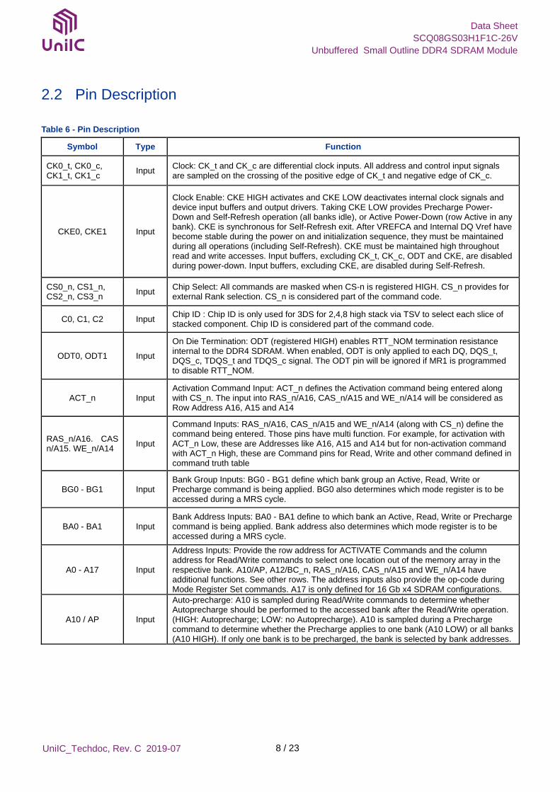
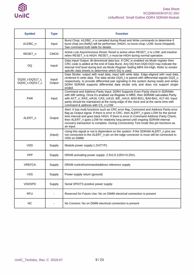
2.2 Pin Description
Table 6 - Pin Description Symbol Type Function
CK0_t, CK0_c, CK1_t, CK1_c
Input Clock: CK_t and CK_c are differential clock inputs. All address and control input signals are sampled on the crossing of the positive edge of CK_t and negative edge of CK_c.
CKE0, CKE1 Input
Clock Enable: CKE HIGH activates and CKE LOW deactivates internal clock signals and device input buffers and output drivers. Taking CKE LOW provides Precharge Power-Down and Self-Refresh operation (all banks idle), or Active Power-Down (row Active in any bank). CKE is synchronous for Self-Refresh exit. After VREFCA and Internal DQ Vref have become stable during the power on and initialization sequence, they must be maintained during all operations (including Self-Refresh). CKE must be maintained high throughout read and write accesses. Input buffers, excluding CK_t, CK_c, ODT and CKE, are disabled during power-down. Input buffers, excluding CKE, are disabled during Self-Refresh.
CS0_n, CS1_n, CS2_n, CS3_n
Input Chip Select: All commands are masked when CS-n is registered HIGH. CS_n provides for external Rank selection. CS_n is considered part of the command code.
C0, C1, C2 Input Chip ID : Chip ID is only used for 3DS for 2,4,8 high stack via TSV to select each slice of stacked component. Chip ID is considered part of the command code.
ODT0, ODT1 Input
On Die Termination: ODT (registered HIGH) enables RTT_NOM termination resistance internal to the DDR4 SDRAM. When enabled, ODT is only applied to each DQ, DQS_t, DQS_c, TDQS_t and TDQS_c signal. The ODT pin will be ignored if MR1 is programmed to disable RTT_NOM.
ACT_n Input Activation Command Input: ACT_n defines the Activation command being entered along with CS_n. The input into RAS_n/A16, CAS_n/A15 and WE_n/A14 will be considered as Row Address A16, A15 and A14
RAS_n/A16. CAS n/A15. WE_n/A14
Input
Command Inputs: RAS_n/A16, CAS_n/A15 and WE_n/A14 (along with CS_n) define the command being entered. Those pins have multi function. For example, for activation with ACT_n Low, these are Addresses like A16, A15 and A14 but for non-activation command with ACT_n High, these are Command pins for Read, Write and other command defined in command truth table
BG0 - BG1 Input Bank Group Inputs: BG0 - BG1 define which bank group an Active, Read, Write or Precharge command is being applied. BG0 also determines which mode register is to be accessed during a MRS cycle.
BA0 - BA1 Input Bank Address Inputs: BA0 - BA1 define to which bank an Active, Read, Write or Precharge command is being applied. Bank address also determines which mode register is to be accessed during a MRS cycle.
A0 - A17 Input
Address Inputs: Provide the row address for ACTIVATE Commands and the column address for Read/Write commands to select one location out of the memory array in the respective bank. A10/AP, A12/BC_n, RAS_n/A16, CAS_n/A15 and WE_n/A14 have additional functions. See other rows. The address inputs also provide the op-code during Mode Register Set commands. A17 is only defined for 16 Gb x4 SDRAM configurations.
A10 / AP Input
Auto-precharge: A10 is sampled during Read/Write commands to determine whether Autoprecharge should be performed to the accessed bank after the Read/Write operation. (HIGH: Autoprecharge; LOW: no Autoprecharge). A10 is sampled during a Precharge command to determine whether the Precharge applies to one bank (A10 LOW) or all banks (A10 HIGH). If only one bank is to be precharged, the bank is selected by bank addresses.
UniIC_Techdoc, Rev. C 2019-07 9 / 23
Data Sheet
SCQ08GS03H1F1C-26V
Unbuffered Small Outline DDR4 SDRAM Module
Symbol Type Function
A12/BC_n Input Burst Chop: A12/BC_n is sampled during Read and Write commands to determine if burst chop (on-thefly) will be performed. (HIGH, no burst chop; LOW: burst chopped). See command truth table for details.
RESET_n CMOS Active Low Asynchronous Reset: Reset is active when RESET_n is LOW, and inactive when RESET_n is HIGH. RESET_n must be HIGH during normal operation.
DQ Input/
Data Input/ Output: Bi-directional data bus. If CRC is enabled via Mode register then CRC code is added at the end of Data Burst. Any DQ from DQ0-DQ3 may indicate the internal Vref level during test via Mode Register Setting MR4 A4=High. Refer to vendor specific data sheets to determine which DQ is used.
DQS0_t-DQS17_t, DQS0_c-DQS17_c
Input/ Output
Data Strobe: output with read data, input with write data. Edge-aligned with read data, centered in write data. The data strobe DQS_t is paired with differential signals DQS_c, respectively, to provide differential pair signaling to the system during reads and writes. DDR4 SDRAM supports differential data strobe only and does not support single-ended.
PAR Input
Command and Address Parity Input: DDR4 Supports Even Parity check in SDRAMs with MR setting. Once it’s enabled via Register in MR5, then SDRAM calculates Parity with ACT_n, RAS_n/A16, CAS_n/A15, WE_n/A14, BG0-BG1, BA0-BA1, A17-A0. Input parity should be maintained at the rising edge of the clock and at the same time with command & address with CS_n LOW
ALERT_n Output
Alert: It has multi functions such as CRC error flag, Command and Address Parity error flag as Output signal. If there is error in CRC, then ALERT_n goes LOW for the period time interval and goes back HIGH. If there is error in Command Address Parity Check, then ALERT_n goes LOW for relatively long period until ongoing SDRAM internal recovery transaction is complete. During Connectivity Test mode this pin functions as an input.
(Input)
Using this signal or not is dependent on the system. If the SDRAM ALERT_n pins are not connected to the ALERT_n pin on the edge connector is must still be connected to VDD on DIMM.
VDD Supply Module power supply:1.2V(TYP).
VPP Supply DRAM activating power supply: 2.5V(-0.125V/+0.25V).
VREFCA Supply DRAM control/command/address reference supply
VSS Supply Power supply return (ground)
VDDSPD Supply Serial SPD/TS positive power supply
RFU - Reserved for Future Use: No on DIMM electrical connection is present
NC - No Connect: No on DIMM electrical connection is present
UniIC_Techdoc, Rev. C 2019-07 10 / 23
Data Sheet
SCQ08GS03H1F1C-26V
Unbuffered Small Outline DDR4 SDRAM Module
3 General Description
3.1 General Description
High-speed DDR4 SDRAM modules use DDR4 SDRAM devices with 2 or 4 internal memory bank groups. DDR4 SDRAM
modules utilizing 4- and 8-bit-wide DDR4 SDRAM have 4 internal bank groups consisting of 4 memory banks each, providing a
total of 16 banks. Sixteen-bit-wide DDR4 SDRAM has 2 internal bank groups consisting of 4 memory banks each, providing a
total of 8 banks. DDR4 SDRAM modules benefit from DDR4 SDRAM's use of an 8n-prefetch architecture with an interface
designed to transfer two data words per clock cycle at the I/O pins. A single READ or WRITE operation for the DDR4 SDRAM
effectively consists of a single 8n-bit-wide, four-clock data transfer at the internal DRAM core and eight corresponding n-bit
wide, one-half-clock-cycle data transfers at the I/O pins.
DDR4 modules use two sets of differential signals: DQS, DQS# to capture data and CK and CK# to capture commands,
addresses, and control signals. Differential clocks and data strobes ensure exceptional noise immunity for these signals and
provide precise crossing points to capture input signals.
3.2 Serial Presence-Detect EEPROM Operation
DDR4 SDRAM modules incorporate serial presence-detect. The SPD data is stored in a 512-byte EEPROM. System
READ/WRITE operations between the master (system logic) and the slave EEPROM device occur via a standard I2C bus
using the DIMM’s SCL (clock) SDA (data), and SA (address) pins. Write protect (WP) is connected to VSS, permanently
disabling hardware write protection.
UniIC_Techdoc, Rev. C 2019-07 11 / 23
Data Sheet
SCQ08GS03H1F1C-26V
Unbuffered Small Outline DDR4 SDRAM Module
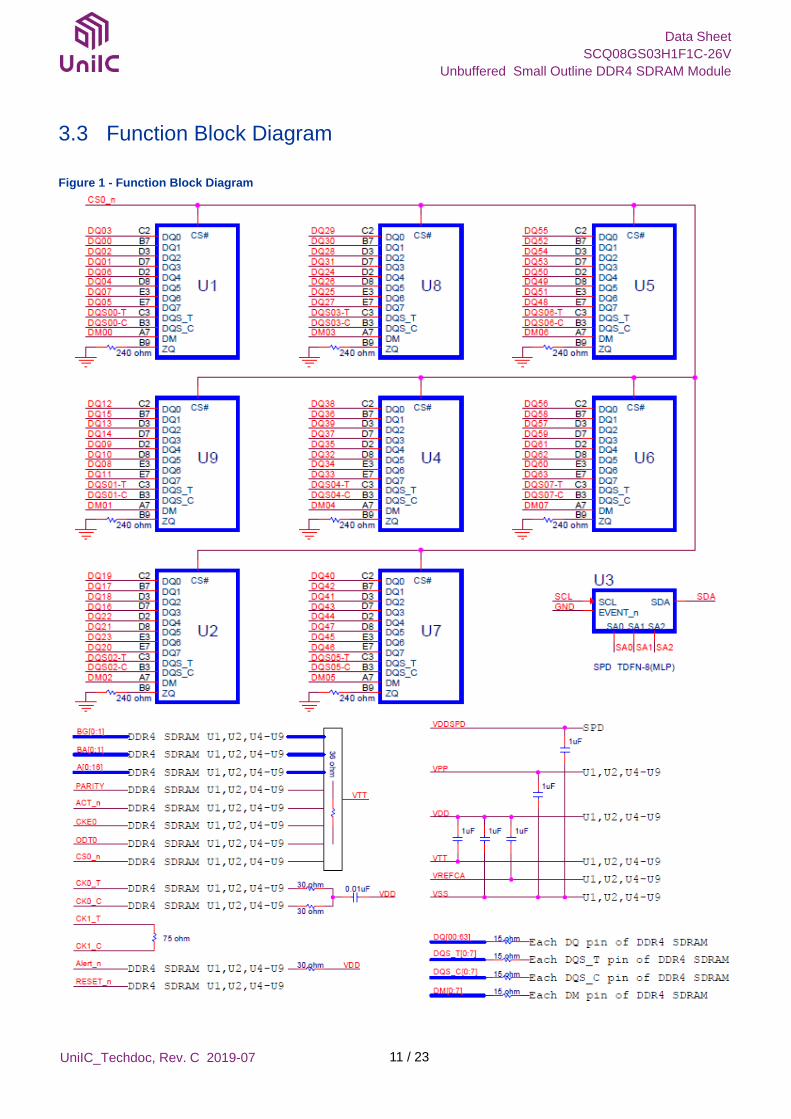
3.3 Function Block Diagram
Figure 1 - Function Block Diagram
UniIC_Techdoc, Rev. C 2019-07 12 / 23
Data Sheet
SCQ08GS03H1F1C-26V
Unbuffered Small Outline DDR4 SDRAM Module
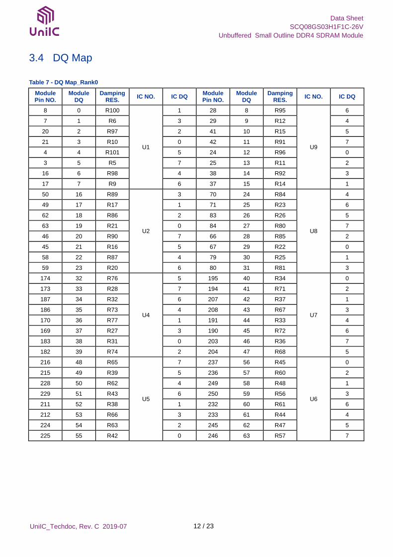
3.4 DQ Map
Table 7 - DQ Map_Rank0
Module Pin NO.
Module DQ
Damping RES.
IC NO. IC DQ Module Pin NO.
Module DQ
Damping RES.
IC NO. IC DQ
8 0 R100
U1
1 28 8 R95
U9
6
7 1 R6 3 29 9 R12 4
20 2 R97 2 41 10 R15 5
21 3 R10 0 42 11 R91 7
4 4 R101 5 24 12 R96 0
3 5 R5 7 25 13 R11 2
16 6 R98 4 38 14 R92 3
17 7 R9 6 37 15 R14 1
50 16 R89
U2
3 70 24 R84
U8
4
49 17 R17 1 71 25 R23 6
62 18 R86 2 83 26 R26 5
63 19 R21 0 84 27 R80 7
46 20 R90 7 66 28 R85 2
45 21 R16 5 67 29 R22 0
58 22 R87 4 79 30 R25 1
59 23 R20 6 80 31 R81 3
174 32 R76
U4
5 195 40 R34
U7
0
173 33 R28 7 194 41 R71 2
187 34 R32 6 207 42 R37 1
186 35 R73 4 208 43 R67 3
170 36 R77 1 191 44 R33 4
169 37 R27 3 190 45 R72 6
183 38 R31 0 203 46 R36 7
182 39 R74 2 204 47 R68 5
216 48 R65
U5
7 237 56 R45
U6
0
215 49 R39 5 236 57 R60 2
228 50 R62 4 249 58 R48 1
229 51 R43 6 250 59 R56 3
211 52 R38 1 232 60 R61 6
212 53 R66 3 233 61 R44 4
224 54 R63 2 245 62 R47 5
225 55 R42 0 246 63 R57 7
UniIC_Techdoc, Rev. C 2019-07 13 / 23
Data Sheet
SCQ08GS03H1F1C-26V
Unbuffered Small Outline DDR4 SDRAM Module
4 Electrical Characteristics
This chapter contains speed grade definition, AC timing parameter and ODT tables.
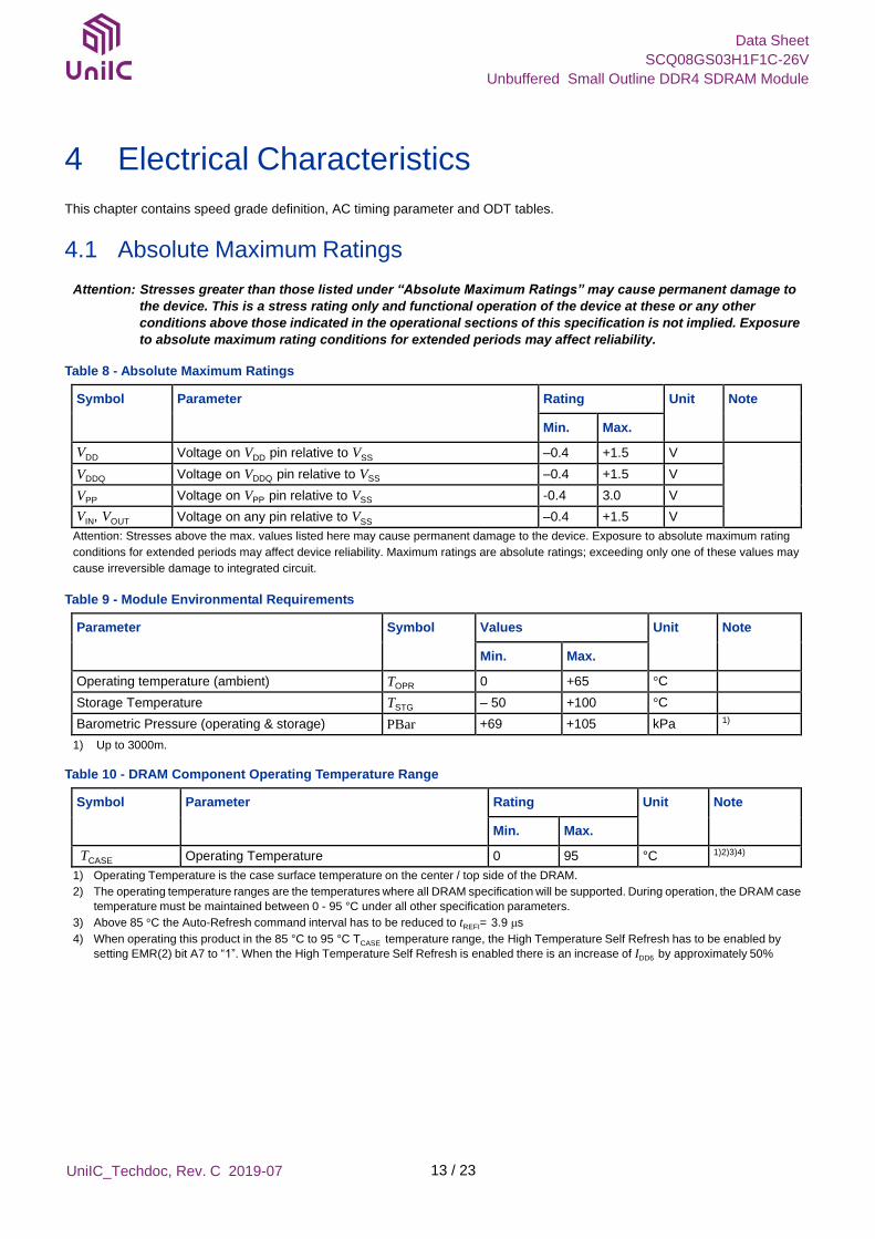
4.1 Absolute Maximum Ratings
Attention: Stresses greater than those listed under “Absolute Maximum Ratings” may cause permanent damage to
the device. This is a stress rating only and functional operation of the device at these or any other
conditions above those indicated in the operational sections of this specification is not implied. Exposure
to absolute maximum rating conditions for extended periods may affect reliability.
Table 8 - Absolute Maximum Ratings
Symbol Parameter Rating Unit Note
Min. Max.
VDD Voltage on VDD pin relative to VSS –0.4 +1.5 V VDDQ Voltage on VDDQ pin relative to VSS –0.4 +1.5 V
VPP Voltage on VPP pin relative to VSS -0.4 3.0 V
VIN, VOUT Voltage on any pin relative to VSS –0.4 +1.5 V Attention: Stresses above the max. values listed here may cause permanent damage to the device. Exposure to absolute maximum rating
conditions for extended periods may affect device reliability. Maximum ratings are absolute ratings; exceeding only one of these values may
cause irreversible damage to integrated circuit.
Table 9 - Module Environmental Requirements
Parameter Symbol Values Unit Note
Min. Max.
Operating temperature (ambient) TOPR 0 +65 °C Storage Temperature TSTG – 50 +100 °C Barometric Pressure (operating & storage) PBar +69 +105 kPa 1)
1) Up to 3000m.
Table 10 - DRAM Component Operating Temperature Range
Symbol Parameter Rating Unit Note
Min. Max.
TCASE Operating Temperature 0 95 °C 1)2)3)4)
1) Operating Temperature is the case surface temperature on the center / top side of the DRAM.
2) The operating temperature ranges are the temperatures where all DRAM specification will be supported. During operation, the DRAM case
temperature must be maintained between 0 - 95 °C under all other specification parameters.
3) Above 85 °C the Auto-Refresh command interval has to be reduced to tREFI= 3.9 μs
4) When operating this product in the 85 °C to 95 °C TCASE temperature range, the High Temperature Self Refresh has to be enabled by
setting EMR(2) bit A7 to “1”. When the High Temperature Self Refresh is enabled there is an increase of IDD6 by approximately 50%
UniIC_Techdoc, Rev. C 2019-07 14 / 23
Data Sheet
SCQ08GS03H1F1C-26V
Unbuffered Small Outline DDR4 SDRAM Module
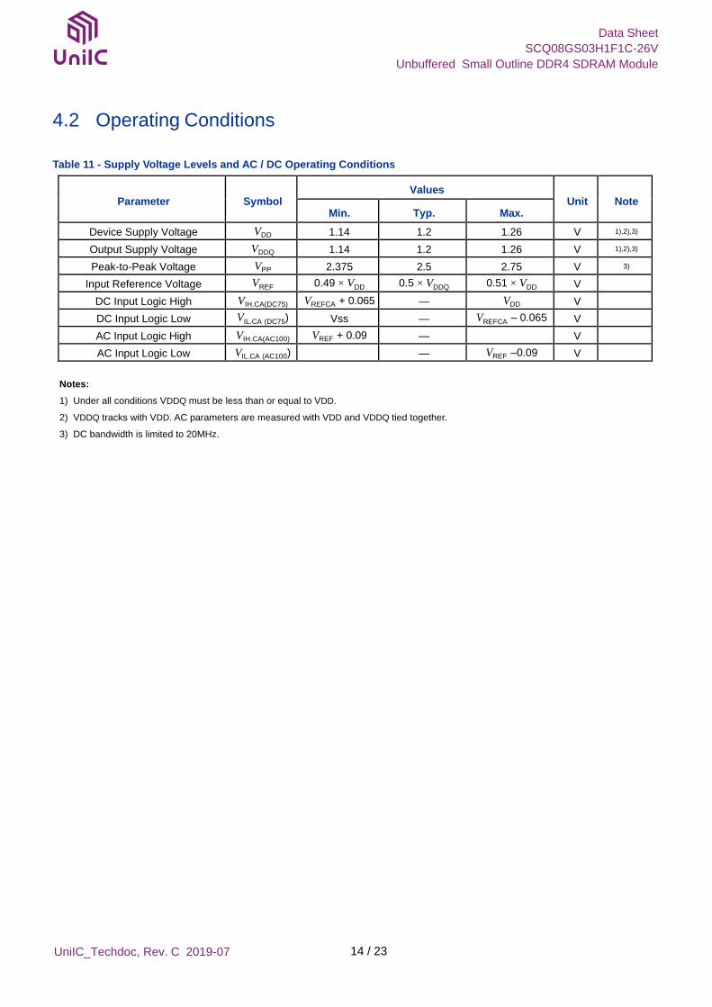
4.2 Operating Conditions
Table 11 - Supply Voltage Levels and AC / DC Operating Conditions
Parameter Symbol Values
Unit Note Min. Typ. Max.
Device Supply Voltage VDD 1.14 1.2 1.26 V 1),2),3)
Output Supply Voltage VDDQ 1.14 1.2 1.26 V 1),2),3)
Peak-to-Peak Voltage VPP 2.375 2.5 2.75 V 3)
Input Reference Voltage VREF 0.49 × VDD 0.5 × VDDQ 0.51 × VDD V DC Input Logic High VIH.CA(DC75) VREFCA + 0.065 — VDD V
DC Input Logic Low VIL.CA (DC75) Vss — VREFCA – 0.065 V
AC Input Logic High VIH.CA(AC100) VREF + 0.09 — V
AC Input Logic Low VIL.CA (AC100) — VREF –0.09 V
Notes:
1) Under all conditions VDDQ must be less than or equal to VDD.
2) VDDQ tracks with VDD. AC parameters are measured with VDD and VDDQ tied together.
3) DC bandwidth is limited to 20MHz.
UniIC_Techdoc, Rev. C 2019-07 15 / 23
Data Sheet
SCQ08GS03H1F1C-26V
Unbuffered Small Outline DDR4 SDRAM Module
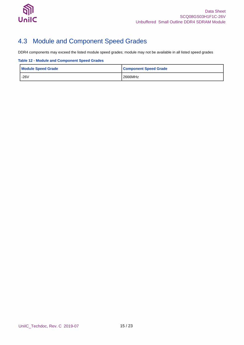
4.3 Module and Component Speed Grades
DDR4 components may exceed the listed module speed grades; module may not be available in all listed speed grades
Table 12 - Module and Component Speed Grades
Module Speed Grade Component Speed Grade
-26V 2666MHz
UniIC_Techdoc, Rev. C 2019-07 16 / 23
Data Sheet
SCQ08GS03H1F1C-26V
Unbuffered Small Outline DDR4 SDRAM Module
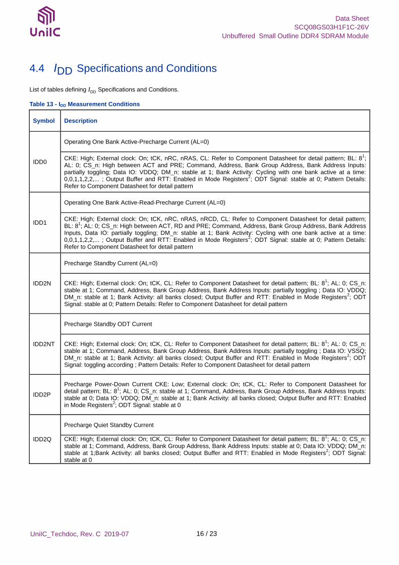
4.4 IDD Specifications and Conditions
List of tables defining IDD Specifications and Conditions.
Table 13 - IDD Measurement Conditions
Symbol Description
IDD0
Operating One Bank Active-Precharge Current (AL=0)
CKE: High; External clock: On; tCK, nRC, nRAS, CL: Refer to Component Datasheet for detail pattern; BL: 81;
AL: 0; CS_n: High between ACT and PRE; Command, Address, Bank Group Address, Bank Address Inputs: partially toggling; Data IO: VDDQ; DM_n: stable at 1; Bank Activity: Cycling with one bank active at a time: 0,0,1,1,2,2,... ; Output Buffer and RTT: Enabled in Mode Registers
2; ODT Signal: stable at 0; Pattern Details:
Refer to Component Datasheet for detail pattern
IDD1
Operating One Bank Active-Read-Precharge Current (AL=0)
CKE: High; External clock: On; tCK, nRC, nRAS, nRCD, CL: Refer to Component Datasheet for detail pattern; BL: 8
1; AL: 0; CS_n: High between ACT, RD and PRE; Command, Address, Bank Group Address, Bank Address
Inputs, Data IO: partially toggling; DM_n: stable at 1; Bank Activity: Cycling with one bank active at a time: 0,0,1,1,2,2,... ; Output Buffer and RTT: Enabled in Mode Registers
2; ODT Signal: stable at 0; Pattern Details:
Refer to Component Datasheet for detail pattern
IDD2N
Precharge Standby Current (AL=0)
CKE: High; External clock: On; tCK, CL: Refer to Component Datasheet for detail pattern; BL: 81; AL: 0; CS_n:
stable at 1; Command, Address, Bank Group Address, Bank Address Inputs: partially toggling ; Data IO: VDDQ; DM_n: stable at 1; Bank Activity: all banks closed; Output Buffer and RTT: Enabled in Mode Registers
2; ODT
Signal: stable at 0; Pattern Details: Refer to Component Datasheet for detail pattern
IDD2NT
Precharge Standby ODT Current
CKE: High; External clock: On; tCK, CL: Refer to Component Datasheet for detail pattern; BL: 81; AL: 0; CS_n:
stable at 1; Command, Address, Bank Group Address, Bank Address Inputs: partially toggling ; Data IO: VSSQ; DM_n: stable at 1; Bank Activity: all banks closed; Output Buffer and RTT: Enabled in Mode Registers
2; ODT
Signal: toggling according ; Pattern Details: Refer to Component Datasheet for detail pattern
IDD2P
Precharge Power-Down Current CKE: Low; External clock: On; tCK, CL: Refer to Component Datasheet for detail pattern; BL: 8
1; AL: 0; CS_n: stable at 1; Command, Address, Bank Group Address, Bank Address Inputs:
stable at 0; Data IO: VDDQ; DM_n: stable at 1; Bank Activity: all banks closed; Output Buffer and RTT: Enabled in Mode Registers
2; ODT Signal: stable at 0
IDD2Q
Precharge Quiet Standby Current
CKE: High; External clock: On; tCK, CL: Refer to Component Datasheet for detail pattern; BL: 81; AL: 0; CS_n:
stable at 1; Command, Address, Bank Group Address, Bank Address Inputs: stable at 0; Data IO: VDDQ; DM_n: stable at 1;Bank Activity: all banks closed; Output Buffer and RTT: Enabled in Mode Registers
2; ODT Signal:
stable at 0
UniIC_Techdoc, Rev. C 2019-07 17 / 23
Data Sheet
SCQ08GS03H1F1C-26V
Unbuffered Small Outline DDR4 SDRAM Module
Symbol Description
IDD3N
Active Standby Current
CKE: High; External clock: On; tCK, CL: Refer to Component Datasheet for detail pattern; BL: 81; AL: 0; CS_n:
stable at 1; Command, Address, Bank Group Address, Bank Address Inputs: partially toggling Data IO: VDDQ; DM_n: stable at 1;Bank Activity: all banks open; Output Buffer and RTT: Enabled in Mode Registers
2; ODT
Signal: stable at 0; Pattern Details:Refer to Component Datasheet for detail pattern
IDD3P
Active Power-Down Current
CKE: Low; External clock: On; tCK, CL: sRefer to Component Datasheet for detail pattern; BL: 81; AL: 0; CS_n:
stable at 1; Command, Address, Bank Group Address, Bank Address Inputs: stable at 0; Data IO: VDDQ; DM_n: stable at 1; Bank Activity: all banks open; Output Buffer and RTT: Enabled in Mode Registers
2; ODT
Signal: stable at 0
IDD4R
Operating Burst Read Current
CKE: High; External clock: On; tCK, CL: Refer to Component Datasheet for detail pattern; BL: 82; AL: 0; CS_n:
High between RD; Command, Address, Bank Group Address, Bank Address Inputs: partially toggling ; Data IO: seamless read data burst with different data between one burst and the next one according ; DM_n: stable at 1; Bank Activity: all banks open, RD commands cycling through banks: 0,0,1,1,2,2,... ; Output Buffer and RTT: Enabled in Mode Registers
2; ODT Signal: stable at 0; Pattern Details: Refer to Component Datasheet for detail
pattern
IDD4W
Operating Burst Write Current
CKE: High; External clock: On; tCK, CL: Refer to Component Datasheet for detail pattern; BL: 81; AL: 0; CS_n:
High between WR; Command, Address, Bank Group Address, Bank Address Inputs: partially toggling ; Data IO: seamless write data burst with different data between one burst and the next one ; DM_n: stable at 1; Bank Activity: all banks open, WR commands cycling through banks: 0,0,1,1,2,2,...; Output Buffer and RTT: Enabled in Mode Registers
2; ODT Signal: stable at HIGH; Pattern Details: Refer to Component Datasheet for detail
pattern
IDD5B
Burst Refresh Current (1X REF) CKE: High; External clock: On; tCK, CL, nRFC: Refer to Component Datasheet for detail pattern; BL: 8
1; AL: 0;
CS_n: High between REF; Command, Address, Bank Group Address, Bank Address Inputs: partially toggling ; Data IO: VDDQ; DM_n: stable at 1; Bank Activity: REF command every nRFC ; Output Buffer and RTT: Enabled in Mode Registers
2; ODT Signal: stable at 0; Pattern Details: Refer to Component Datasheet for detail
pattern
IDD6N
Self Refresh Current: Normal Temperature Range Tcase: 0 - 85°C; Low Power Array Self Refresh (LP ASR) : Normal4; CKE: Low; External clock: Off; CK_t and CK_c#: LOW; CL: Refer to Component Datasheet for detail pattern; BL: 81; AL: 0; CS_n#, Command, Address, Bank Group Address, Bank Address, Data IO: High; DM n: stable at 1; Bank Activity: Self-Refresh operation; Output Buffer and RTT: Enabled in Mode Registers2; ODT Signal: MIDLEVEL
IDD6N
Self-Refresh Current: Extended Temperature Range) TCase: 0 - 95°C; Low Power Array Self Refresh (LP ASR) : Extended4; CKE: Low; External clock: Off; CK_t and CK_c: LOW; CL: Refer to Component Datasheet for detail pattern; BL: 81; AL: 0; CS_n, Command, Address, Bank Group Address, Bank Address, Data IO: High; DM_n:stable at 1; Bank Activity: Extended Temperature Self-Refresh operation; Output Buffer and RTT: Enabled in Mode Registers2; ODT Signal: MID-LEVEL
UniIC_Techdoc, Rev. C 2019-07 18 / 23
Data Sheet
SCQ08GS03H1F1C-26V
Unbuffered Small Outline DDR4 SDRAM Module
Symbol Description
IDD6R
Self-Refresh Current: Reduced Temperature Range
TCase: 0 - 45°C; Low Power Array Self Refresh (LP ASR) : Reduced4; CKE: Low; External clock: Off; CK_t and
CK_c#: LOW; CL: Refer to Component Datasheet for detail pattern; BL: 81; AL: 0; CS_n#, Command, Address,
Bank Group Address, Bank Address, Data IO: High; DM_n:stable at 1; Bank Activity: Extended Temperature Self-Refresh operation; Output Buffer and RTT: Enabled in Mode Registers
2; ODT Signal: MID-LEVEL
IDD6A
Auto Self-Refresh Current
TCase: 0 - 95°C; Low Power Array Self Refresh (LP ASR) : Auto4; CKE: Low; External clock: Off; CK_t and
CK_c#: LOW; CL: Refer to Component Datasheet for detail pattern; BL: 81; AL: 0; CS_n#, Command, Address,
Bank Group Address, Bank Address, Data IO: High; DM_n:stable at 1; Bank Activity: Auto Self-Refresh operation; Output Buffer and RTT: Enabled in Mode Registers
2; ODT Signal: MID-LEVEL
IDD7
Operating Bank Interleave Read Current
CKE: High; External clock: On; tCK, nRC, nRAS, nRCD, nRRD, nFAW, CL: Refer to Component Datasheet for detail pattern; BL: 8
1; AL: CL-1; CS_n: High between ACT and RDA; Command, Address, Bank Group
Address, Bank Address Inputs: partially toggling ; Data IO: read data bursts with different data between one
burst and the next one ; DM_n: stable at 1; Bank Activity: two times interleaved cycling through banks (0,
1, ...7) with different addressing; Output Buffer and RTT: Enabled in Mode Registers2; ODT Signal: stable at 0;
Pattern Details: Refer to Component Datasheet for detail pattern
IDD8 Maximum Power Down Current TBD
Notes : 1. Burst Length: BL8 fixed by MRS: set MR0 [A1:0=00].
2. Output Buffer Enable - set MR1 [A12 = 0] : Qoff = Output buffer enabled - set MR1 [A2:1 = 00] : Output Driver Impedance Control = RZQ/7 RTT_Nom
enable - set MR1 [A10:8 = 011] : RTT_NOM = RZQ/6 RTT_WR enable - set MR2 [A10:9 = 01] : RTT_WR = RZQ/2 RTT_PARK disable - set MR5 [A8:6
= 000]
3. CAL enabled : set MR4 [A8:6 = 001] : 1600MT/s 010] : 1866MT/s, 2133MT/s 011] : 2400MT/s Gear Down mode enabled :set MR3 [A3 = 1] : 1/4 Rate
DLL disabled : set MR1 [A0 = 0] CA parity enabled :set MR5 [A2:0 = 001] : 1600MT/s,1866MT/s, 2133MT/s 010] : 2400MT/s Read DBI enabled : set
MR5 [A12 = 1] Write DBI enabled : set :MR5 [A11 = 1]
4. Low Power Array Self Refresh (LP ASR) : set MR2 [A7:6 = 00] : Normal 01] : Reduced Temperature range 10] : Extended Temperature range 11] :
Auto Self Refresh
TABLE 15 Definitions for IDD
UniIC_Techdoc, Rev. C 2019-07 19 / 23
Data Sheet
SCQ08GS03H1F1C-26V
Unbuffered Small Outline DDR4 SDRAM Module
Table 14 - IDD Specification for SCQ08GS03H1F1C-26V
Product Type SCQ08GS03H1F1C-26V Unit Note1)2)
Organization 8GB
1Rank (×8)
×64
-26V
Symbol Max.
IDD0 320 mA 3)
IDD1 408 mA 3)
IDD2N 232 mA 4)
IDD2NT 280 mA 3)
IDD2P 152 mA 4)
IDD2Q 192 mA 4)
IDD3N 376 mA 4)
IDD3P 304 mA 4)
IDD4R 1072 mA 3)
IDD4W 1048 mA 3)
IDD5B 1800 mA 3)
IDD6N 176 mA 4)
IDD6E 224 mA 4)
IDD6R 112 mA 4)
IDD6A 224 mA 4)
IDD7 1280 mA 3)
IDD8 96 mA 4)
1) Calculated values from component data.
2) IDDX (rank) = Number of components x IDDX (component)
3) IDDX = IDDX (rank) +(Rank-1)* IDD2P (rank)
4) IDDX = Rank * IDDX (rank)
UniIC_Techdoc, Rev. C 2019-07 20 / 23
Data Sheet
SCQ08GS03H1F1C-26V
Unbuffered Small Outline DDR4 SDRAM Module
5 Package Dimensions
Figure 2 - Package Dimensions
UniIC_Techdoc, Rev. C 2019-07 21 / 23
Data Sheet
SCQ08GS03H1F1C-26V
Unbuffered Small Outline DDR4 SDRAM Module
List of Figures
Figure 1 - Function Block Diagram .............................................................................................................................................. 11 Figure 2 - Package Dimensions .................................................................................................................................................. 20
UniIC_Techdoc, Rev. C 2019-07 22 / 23
Data Sheet
SCQ08GS03H1F1C-26V
Unbuffered Small Outline DDR4 SDRAM Module
List of Tables
Table 1 - Module Performance Table ............................................................................................................................................. 4 Table 2 - Ordering Information ....................................................................................................................................................... 5 Table 3 - Address Format .............................................................................................................................................................. 5 Table 4 - Components on Modules ................................................................................................................................................ 5 Table 5 - Pin Configuration SODIMM (260 pin) ............................................................................................................................. 6 Table 6 - Pin Description ............................................................................................................................................................... 8 Table 7 - DQ Map_Rank0 ............................................................................................................................................................ 12 Table 8 - Absolute Maximum Ratings .......................................................................................................................................... 13 Table 9 - Module Environmental Requirements ........................................................................................................................... 13 Table 10 - DRAM Component Operating Temperature Range .................................................................................................... 13 Table 11 - Supply Voltage Levels and AC / DC Operating Conditions ......................................................................................... 14 Table 12 - Module and Component Speed Grades ..................................................................................................................... 15 Table 13 - IDD Measurement Conditions ...................................................................................................................................... 16 Table 14 - IDD Specification for SCQ08GS03H1F1C-26V ............................................................................................................ 19
UniIC_Techdoc, Rev. C 2019-07 23 / 23
Data Sheet
SCQ08GS03H1F1C-26V
Unbuffered Small Outline DDR4 SDRAM Module
Edition 2019-07
Published by
Xi’an UniIC Semiconductors Co., Ltd.
Xi’an: 4th Floor, Building A,
No. 38 Gaoxin 6th Road,
Xian High-tech Industries Development Zone
Xi'an, Shaanxi 710075, P. R. China
Tel: +86-29-88318000
Fax: +86-29-88453299
© UniIC 2019.
All Rights Reserved.
Legal Disclaimer
THE INFORMATION GIVEN IN THIS INTERNET DATA SHEET SHALL IN NO EVENT BE REGARDED AS A GUARANTEE
OF CONDITIONS OR CHARACTERISTICS. WITH RESPECT TO ANY EXAMPLES OR HINTS GIVEN HEREIN, ANY
TYPICAL VALUES STATED HEREIN AND/OR ANY INFORMATION REGARDING THE APPLICATION OF THE DEVICE,
UNIIC HEREBY DISCLAIMS ANY AND ALL WARRANTIES AND LIABILITIES OF ANY KIND, INCLUDING WITHOUT
LIMITATION WARRANTIES OF NON-INFRINGEMENT OF INTELLECTUAL PROPERTY RIGHTS OF ANY THIRD PARTY.
Information
For further information on technology, delivery terms and conditions and prices please contact your nearest UniIC Office.
Warnings
Due to technical requirements components may contain dangerous substances. For information on the types in question
please contact your nearest UniIC Office.
UniIC Components may only be used in life-support devices or systems with the express written approval of UniIC, if a failure
of such components can reasonably be expected to cause the failure of that life-support device or system, or to affect the
safety or effectiveness of that device or system. Life support devices or systems are intended to be implanted in the human
body, or to support and/or maintain and sustain and/or protect human life. If they fail, it is reasonable to assume that the health
of the user or other persons may be endangered.
www.unisemicon.com