data sheet - download.icxbk.comdownload.icxbk.com/201707/688d81adcf72e29d4e92f303a7c3f5b9.pdf ·...
TRANSCRIPT

Ingenic® Jz4730 Processor
Data Sheet
Confidential
® Ingenic Semiconductor Co.Limited

Packaging and Pinout Information
Contents
CHAPTER 1 PRODUCT OVERVIEW ............................................................................................................1 1.1 PROCESSOR BLOCK DIAGRAM ....................................................................................................................1 1.2 PROCESSOR FEATURES ...............................................................................................................................2
1.2.1 JzRISC Core.......................................................................................................................................2 1.2.2 System Control and Timers ................................................................................................................2 1.2.3 Memory Interface...............................................................................................................................2 1.2.4 Inter-chip Connectivity ......................................................................................................................3 1.2.5 Connectivity and Expansion...............................................................................................................3 1.2.6 Multimedia Interface..........................................................................................................................4 1.2.7 Clock and Power Management ..........................................................................................................4
CHAPTER 2 PACKAGING AND PINOUT INFORMATION ......................................................................5 2.1 OVERVIEW..................................................................................................................................................5 2.2 PIN DESCRIPTION........................................................................................................................................6 2.3 PACKAGE DIMENSION...............................................................................................................................16 2.4 BALL ASSIGNMENT...................................................................................................................................17 2.5 PACKAGE POWER RATINGS ......................................................................................................................19
CHAPTER 3 ELECTRICAL SPECIFICATIONS ........................................................................................20 3.1 ABSOLUTE MAXIMUM RATINGS ...............................................................................................................20 3.2 POWER CONSUMPTION SPECIFICATIONS ...................................................................................................20 3.3 OPERATING CONDITIONS ..........................................................................................................................22 3.4 DC SPECIFICATIONS .................................................................................................................................22 3.5 AC SPECIFICATIONS .................................................................................................................................24 3.6 OSCILLATOR ELECTRICAL SPECIFICATIONS..............................................................................................24
3.6.1 32.768KHz Oscillator Specifications ...............................................................................................24 3.6.2 3.6864MHz Oscillator Specifications ..............................................................................................24
3.7 RESET AND POWER AC TIMING SPECIFICATIONS .....................................................................................24 3.7.1 Power-On Timing.............................................................................................................................25 3.7.2 Hardware Reset Timing ...................................................................................................................26
3.8 MEMORY BUS AND PCMCIA AC SPECIFICATIONS ..................................................................................26 3.9 PERIPHERAL MODULE AC SPECIFICATIONS..............................................................................................27
3.9.1 LCD Module Timing ........................................................................................................................27 3.9.2 CIM Module Timing.........................................................................................................................27 3.9.3 SPI Module Timing ..........................................................................................................................27 3.9.4 External DMA Request and Grant ...................................................................................................27
Jz4730 Processor Data Sheet Confidential


Packaging and Pinout Information
Chapter 1 Product Overview
The Jz4730 processor is the competitive product of application processor, which meet the demand of the portable handheld market. Incorporate the JzRISC core based on leading microarchitecture technology, this processor provides high integration, high performance and low power consumption solution for embedded device. The JzRISC is the advanced and power-efficient 32-bit RISC core with 16K I-Cache and 16K D-Cache in this processor, operating at speeds up to 400MHz. On-chip modules such as LCD controller, AC97/I2S controller and camera interface offer designers a rich suite of peripherals for multimedia application. The memory interface supports a variety of memory types that allow flexible design requirements, include the glueless connection to NAND Flash for cost sensitive applications. WLAN, Bluetooth and expansion options are provided through the PCMCIA/CF, USB, and MMC/SD host controllers. And the other peripherals such as UART, SPI, and Ethernet controller as well as general-system resources provide enough compute and connectivity capability for many applications. For the processor block diagram, refer to .
1.1 Processor Block Diagram
Jz4730 Processor Data Book 1

Packaging and Pinout Information
1.2 Processor Features
1.2.1 JzRISC Core JzRISC core is a high performance and low power microprocessor core. • 32-bit RISC CPU, clock up to 400MHz • Low power consumption – <0.5mW/MHz • 16K I-Cache + 16K D-Cache • MMU support with I-TLB, D-TLB and J-TLB • Hardware Debug support via JTAG port
1.2.2 System Control and Timers
• Interrupt controller ― Total 28 maskable interrupt sources from on-chip peripherals and external request
through GPIO ports ― Interrupt source and pending registers for software handling ― Unmasked interrupts can wake up the chip in sleep or standby mode
• Operating system timer ― Provide three separate channels ― 32-bit counter with auto-reload function ― Generate interrupt when the down counter underflows ― Six counting clock sources: RTCCLK (real time clock), EXTAL (external clock input),
φ/4, φ/16, φ/64 and φ/256. (φ is the internal clock for on-chip peripheral) • Watchdog timer
― 32-bit counter with RTC clock ― Generate power-on reset
• Pulse Width Modulator (PWM) ― Period control through a 6-bit clock divider and a 10-bit period counter ― 10-bit pulse counter
• General-Purpose I/O ports ― Total GPIO pin number is 128 ― Each pin can be configured as general-purpose input or output or multiplexed with
internal chip functions ― Each pin can act as a interrupt source and has configurable rising/falling edge or
high/low level detect manner, and can be masked independently ― Each pin can be configured as open-drain when output
1.2.3 Memory Interface
• Static memory interface ― Direct interface to SRAM, ROM, Burst ROM, and NOR Flash ― Six chip-select pin for static memory, each can be configured separately ― Support 8, 16 or 32 bits data width ― The size and base address of static memory banks are programmable
• NAND Flash interface ― Support on CS3, sharing with static memory bank 3 ― Support all 8-bit/16-bit NAND Flash devices regardless of density and organization ― Hardware ECC generation ― Support automatic boot up from NAND Flash devices
• Synchronous DRAM Interface ― 2 banks with programmable size and base address ― 32-bit and 16-bit data bus width is supported ― Multiplexes row/column addresses according to SDRAM capacity ― Two-bank or four-bank SDRAM is supported
Jz4730 Processor Data Book 2
Packaging and Pinout Information
― Supports auto-refresh and self-refresh functions ― Supports power-down mode to minimize the power consumption of SDRAM ― Supports page mode
• PC Card Interface ― Fully compliant with the release of March 1997 of PC Card standard (16-bit PC Card) ― DMA transfer support ― Supports two PCMCIA or CF socket
• Direct Memory Access Controller ― Eight independent DMA channels ― Transfer data units: 8-bit, 16-bit, 32-bit, 16-byte or 32-byte ― Transfer requests can be: auto-request within DMA; on-chip peripheral module request;
and external request ― Interrupt on transfer completion or transfer error ― Supports two transfer modes: single mode or block mode
• The Jz4730 processor system supports little endian only
1.2.4 Inter-chip Connectivity
• I2C bus interface ― Only supports single master mode ― Supports I2C standard-mode and F/S-mode up to 400 kHz ― Double-buffered for receiver and transmitter ― Supports general call address and START byte format after START condition
• Synchronous serial interface ― Supports three formats: TI’s SSP, National Microwire, and Motorola’s SPI ― Configurable 2 - 17 (or multiples of them) bits data transfer ― Full-duplex/transmit-only/receive-only operation ― Supports normal transfer mode or Interval transfer mode ― Programmable transfer order: MSB first or LSB first ― 17-bit width, 16-level deep transmit-FIFO and receive-FIFO ― Programmable divider/prescaler for SSI clock ― Back-to-back character transmission/reception mode
1.2.5 Connectivity and Expansion
• Four UART interface ― 5, 6, 7 or 8 data bit operation with 1 or 1.5 or 2 stop bits, programmable parity (even,
odd, or none) ― 16x8bit FIFO for transmit and 16x11bit FIFO for receive data ― Programmable baud rate up to 230.4Kbps ― Interrupt support for transmit, receive (data ready or timeout), and line status ― Supports DMA transfer mode ― Provide complete serial port signal for modem control functions ― Support slow infrared asynchronous interface (IrDA)
• Two smart card controller ― Compliant with ISO/IEC standard 7816-3, supports both normal smart card and UIM
card interface ― Support asynchronous character (T = 0)/ block (T = 1) communication modes ― 8-bit, 16-level FIFO, and programmable SCC_CLK output clock frequency ― Interrupt support for data communication and error handling
• USB host interface ― Open Host Controller Interface (OHCI)-compatible and USB Revision 1.1-compatible
• USB device interface ― Compliant with USB protocol revision 1.1 ― Supports suspend/resume and remote wakeup ― Supports 8 physical endpoints and 9 logic endpoints
Jz4730 Processor Data Book 3
Packaging and Pinout Information
― Supports bulk, isochronous, interrupt and control transaction • Ethernet MAC interface
― Compliant with IEEE802.3, 802.3u ― 10/100 Mbps data transfer rates with full and half duplex modes ― IEEE802.3 compliant MII interface to talk to an external PHY ― VLAN support ― 2K bytes Tx buffers, and 2K bytes Rx buffers ― Supports DMA engine using burst mode ― Supports remote wake-up frame and magic packet frame
1.2.6 Multimedia Interface
• LCD ― Single-panel display in active mode, and single- or dual-panel displays in passive mode ― Up to 64K colors in active mode, and up to 4096 colors in passive mode ― Display size up to 800×600 pixels ― 256×16 bits internal palette RAM ― Support ITU601/656 data format
• AC97/I2S controller ― Supports 16, 18 and 20 bit sample for AC-link format, and 8, 16, 18, 20 and 24 bit for
I2S/MSB-Justified format ― DMA transfer mode support ― Programmable Output channels and Input channels or Fixed mode for AC-link format ― Power down mode and two wake-up mode support for AC-link format ― Programmable Interrupt function support
• Camera interface ― Input image size up to 2048×2048 pixels ― Supports CCIR656 data format ― 32×32 image data receive FIFO with DMA support
• MultiMedia Card/Secure Digital Controller ― Compliant with “The MultiMediaCard System Specification version 3.3” ― Compliant with “SD Memory Card Specification version 1.01” and “SDIO Card
Specification version 1.0” with 1 command channel and 4 data channels ― 20~80 Mbps maximum data rate ― Supports up to 10 cards (including one SD card) ― Maskable hardware interrupt for SD I/O interrupt, internal status, and FIFO status
1.2.7 Clock and Power Management
• Clock generation Module ― On-chip 3.6864MHz oscillator circuit ― One On-chip phase-locked loops (PLL) with programmable multiple-ratio. Internal
counter are used to ensure PLL stabilize time ― PLL on/off is programmable by software ― ICLK, PCLK, SCLK, MCLK and LCLK frequency can be changed separately for
software by setting division ratio • Power Manager
― support six low-power modes and function: NORMAL mode; DOZE mode; IDLE mode; SLEEP mode; HIBERNATE mode; and MODULE-STOP function.
Jz4730 Processor Data Book 4

Packaging and Pinout Information
Chapter 2 Packaging and Pinout Information
2.1 Overview Jz4730 processor is packaged in a 256-pin ball grid array (LFBGA), has a square 17x17 and 4 rows ball assignment. The following figures and tables list all the functional pins. Most of the GPIO pins are multiplexed on the on-chip peripheral modules, and the reset state is general-purpose input with internal pull-up or pull-down.
Jz4730 Processor Data Book 5

Packaging and Pinout Information
2.2 Pin Description
JTAG
TDO
TDI
TMS
TCK
TRSTN_
MSC / GPIO
signals
AIC / GPIO
signals
PSKTSEL / GP91/TP[2]
PCMCIA / CF / GPIO signals
IOIS16_ / GP92/TP[3]
PCE2_ / GP93/TP[0]
PCE1_ / GP90/TP[1]
TAP_MD
BOOTSEL[3:0]
MSC_DAT [3:0] / GP37~34
PBVD2 / GP89
INPACK_ / GP88
MSC_CMD / GP38
MSC_CLK / GP39
ACRESET_ / GP69
SYSCLK / GP68
BITCLK / GP77
SDATA_IN / GP71
SDATA_OUT / GP70
SYNC / GP78
SDA
SCK I2C
D [31:0]
PWM1 / GP95
PWM0 / GP94PWM / GPIO
signals
XTAL 1~0
EXTAL 1~0
TEST_MODE
System
RESETP_
RESETOUT_
RTCCLK
CIM_D [7:0] / GP7~0
CIM_MCLK / GP11 / TP4
CIM_HSYNC / GP9
CIM_VSYNC / GP8
CIM / GPIO
signals
CIM PCLK / GP10
Jz4730 [256 pins]
(1)
DCS1 / GP82
RB_ / GP81
FEW_ / GP80
FRE_ / GP79
WE3_
WE2_ /
A [25:0]
WAIT_ / PWAIT_
WE1_ / PIOR_
WE0_ / PIOW_
Memory bus / GPIO
signals
DCS0_
CS0
CKO
CKE
RDWR_
RD_ / POE_
WE_ / PWE_
CAS_
RAS_
CS_ [5:1] / GP87~83
Figure 2-1 Jz4730 Pin Diagram (1)
Jz4730 Processor Data Book 6

Packaging and Pinout Information
GPIO signals
GP110~96
PS2_KCLK / GP32
PS2_KDATA / GP33
VDD/VSS (IO2)Supply VDD/VSS (IO1)
PS2 / GPIO
signals
Jz4730® [256 pins]
(2)
UART1_TxD / GP25
UART1_RxD / GP24
UART0_TxD / GP127
UART0_RxD / GP126
SCC0_DATA / GP64
SCC1_DATA / GP65
SCC0_CLK / GP66
SCC1_CLK / GP67
SCC / GPIO signals
MII_COL / GP115
MII_CRS / GP116
MII_TX_CLK
MII_TXD [3:0] / GP120~117
MAC/GPIO signals
MII_TX_EN / GP112
MII RX CLK
MII_RX_DV / GP113
MII_RXD [3:0] / GP124~121
MII_RX_ER / GP114
MII_MDC
MII MDIO
DPLS0
DMNS0
PPWR0 / GP29
OVC0 / TEST_SENUHC / GPIO
signals
UART2 / UART1 / UART0 /
GPIO signals
UART2_TxD / GP125
UART2_RxD / GP111
UART3_RTS_ / GP23/TP[8]
UART3_CTS# / GP17
UART3 / GPIO
signals
UART3_TxD / GP21
UART3_RxD / GP16
VDD/VSS(core)
SSI_CLK / GP72
SSI_CE1_ / GP73
SSI_DT / GP74
SSI_DR / GP75SSI / GPIO
signals
SSI_CE2_ / TP[9] / SPI_GPC / GP76
LCD / GPIO
signals
USB_CLK / GP28
AEN / GP26DMA / GPIO
signals
D 3ACK0 / GP1EOP / GP27
DREQ0 / GP12
DPLS1
DMNS1
LCD_REV / GP63
LCD_PS / GP62
LCD_CLS / GP61
LCD VSYNC / GP56
LCD_HSYNC / GP57
LCD_PCLK / GP58
LCD_DE / GP59
LCD_D [7:0] / GP47~40
LCD_SPL / GP60
LCD_D [15:8] / GP55~48 / TP_MD [17:10]
Figure 2-2 Jz4730 Pin Diagram (2)
Jz4730 Processor Data Book 7

Packaging and Pinout Information
Table 2-1 EMC Pins (81 for 256; 9 GPIO)
Pin Name Type Description Comments D[31:16] I/O Memory data bus, used for 32-bit memories D[15:0] I/O Memory data bus, lower 16 bits of the data bus A[25:17] Output Static memory address
A[16:2] Output SDRAM memory address, multiplexing static memory address
A[1:0] Output Static memory address DCS0_ Output SDRAM chip select 0 DCS1 / GP82 I/O SDRAM chip select 1 /
GPIO 82 Pull-up input at reset
RAS_ Output Row address strobe for SDRAM CAS_ Output Column address strobe for SDRAM CKE Output Clock enable for SDRAM RDWR_ Output Read/write signal, 1 – read; 0 – write CKO Output SDRAM clock CS0_ Output Static memory bank 0 chip select CS1_ / GP83 I/O Static memory bank 1 chip select /
GPIO 83 Pull-up input at reset
CS2_ / GP84 I/O Static memory bank 2 chip select /
GPIO 84 Pull-up input at reset
CS3_ / GP85 I/O Static memory bank 3 chip select /
GPIO 85 Pull-up input at reset
CS4_ / GP86 I/O Static memory bank 4 chip select /
GPIO 86 Pull-up input at reset
CS5_ / GP87 I/O Static memory bank 5 chip select /
GPIO 87 Pull-up input at reset
RD_ / POE_ Output Read strobe for static memory device /
Pcmcia memory read strobe
WE_ / PWE_ Output Write strobe for static memory device /
Pcmcia memory write strobe
WE0_ / PIOW_ Output Byte 0 write enable /
pcmcia IO write strobe
WE1_ / PIOR_ Output Byte 1 write enable /
pcmcia IO read strobe
WE2_ / PREG_ Output Byte 2 write enable /
pcmcia register select
WE3_ Output Byte 3 write enable WAIT_ / PWAIT_ Input Wait signal for slow memory /
pcmcia wait input Internal pull-up
FRE_ / GP79 I/O Read enable for NAND Flash /
GPIO 79 Pull-up input at reset
FWE_ / GP80 I/O Write enable for NAND Flash /
GPIO 80 Pull-up input at reset
FRB_ / GP81 I/O Ready or busy signal for NAND Flash /
GPIO 81 Pull-up input at reset
Jz4730 Processor Data Book 8

Packaging and Pinout Information
Table 2-2 PCMCIA/CF Pins (6 for 256; 6 GPIO)
Pin Name Type Description Comments IOIS16_ / GP92 / TP[3]
I/O PCMCIA IO address 16 bit select / GPIO 92 / Test port [3]
Pull-up input at reset
PSKTSEL / GP91 / TP[2]
I/O PCMCIA socket select / GPIO 91 / Test port [2]
Pull-up input at reset
PCE1_ / GP90 / TP[1]
I/O PCMCIA card enable 1 / GPIO 90 / Test port [1]
Pull-up input at reset
PCE2_ / GP93 / TP[0]
I/O PCMCIA card enable 2 / GPIO 93 / Test port [0]
Pull-up input at reset
INPACK_ / GP88 I/O PCMCIA INPACK_ input /
GPIO 88 Pull-up input at reset
PBVD2 / GP89 I/O PCMCIA BVD2 input /
GPIO89 Pull-up input at reset
Table 2-3 LCD Pins (24 for 256; 24 GPIO)
Pin Name Type Description Comments LCD_D[15:8] / GP55 ~ GP48 / TP[17:10]
I/O Higher 8-bit of LCD data / GPIO 55 ~ GPIO 48 / Test port [17:10]
Pull-down input at reset
LCD_D[7:0] / GP47 ~ GP40 I/O Lower 8-bit of LCD data /
GPIO 47 ~ GPIO 40 Pull-up input at reset
LCD_VSYNC / GP56 I/O LCD frame clock/vertical sync /
GPIO 56 Pull-down input at reset
LCD_HSYNC / GP57 I/O LCD line clock/horizonal sync /
GPIO 57 Pull-up input at reset
LCD_PCLK / GP58 I/O LCD pixel clock /
GPIO 58 Pull-down input at reset
LCD_DE / GP59 I/O STN AC bias drive/Non-STN data enable output /
GPIO 59 Pull-down input at reset
LCD_SPL / GP60 I/O LCD SPL output for special TFT panel /
GPIO 60 Pull-up input at reset
LCD_CLS / GP61 I/O LCD CLS output for special TFT panel /
GPIO 61 Pull-up input at reset
LCD_PS / GP62 I/O LCD PS output for special TFT panel /
GPIO 62 Pull-up input at reset
LCD_REV / GP63 I/O LCD REV output for special TFT panel /
GPIO 63 Pull-up input at reset
Table 2-4 I2C Pins (2 for 256)
Pin Name Type Description Comments I2C_SDA I/O I2C serial data Open drain I2C_SCK I/O I2C serial clock Open drain
Jz4730 Processor Data Book 9
Packaging and Pinout Information
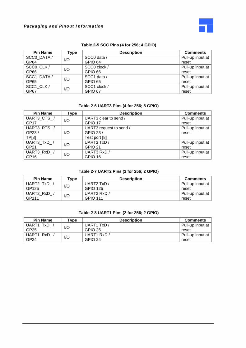
Table 2-5 SCC Pins (4 for 256; 4 GPIO)
Pin Name Type Description Comments SCC0_DATA / GP64 I/O SCC0 data /
GPIO 64 Pull-up input at reset
SCC0_CLK / GP66 I/O SCC0 clock /
GPIO 66 Pull-up input at reset
SCC1_DATA / GP65 I/O SCC1 data /
GPIO 65 Pull-up input at reset
SCC1_CLK / GP67 I/O SCC1 clock /
GPIO 67 Pull-up input at reset
Table 2-6 UART3 Pins (4 for 256; 8 GPIO)
Pin Name Type Description Comments UART3_CTS_ / GP17 I/O UART3 clear to send /
GPIO 17 Pull-up input at reset
UART3_RTS_ / GP23 / TP[8]
I/O UART3 request to send / GPIO 23 / Test port [8]
Pull-up input at reset
UART3_TxD_ / GP21 I/O UART3 TxD /
GPIO 21 Pull-up input at reset
UART3_RxD_ / GP16 I/O UART3 RxD /
GPIO 16 Pull-up input at reset
Table 2-7 UART2 Pins (2 for 256; 2 GPIO)
Pin Name Type Description Comments UART2_TxD_ / GP125 I/O UART2 TxD /
GPIO 125 Pull-up input at reset
UART2_RxD_ / GP111 I/O UART2 RxD /
GPIO 111 Pull-up input at reset
Table 2-8 UART1 Pins (2 for 256; 2 GPIO)
Pin Name Type Description Comments UART1_TxD_ / GP25 I/O UART1 TxD /
GPIO 25 Pull-up input at reset
UART1_RxD_ / GP24 I/O UART1 RxD /
GPIO 24 Pull-up input at reset
Jz4730 Processor Data Book 10

Packaging and Pinout Information
Table 2-9 UART0 Pins (2 for 256; 2 GPIO)
Pin Name Type Description Comments UART0_TxD_ / GP127 I/O UART0 TxD /
GPIO 127 Pull-up input at reset
UART0_RxD_ / GP126 I/O UART0 RxD /
GPIO 126 Pull-up input at reset
Table 2-10 SSI Pins (5 for 256; 5 GPIO)
Pin Name Type Description Comments SSI_CLK / GP72 I/O SSI clock output /
GPIO 72 Pull-up input at reset
SSI_CE1_ / GP73 I/O SSI chip enable 1 /
GPIO 73 Pull-up input at reset
SSI_DT / GP74 I/O SSI data output /
GPIO 74 Pull-up input at reset
SSI_DR / GP75 I/O SSI data input /
GPIO 75 Pull-up input at reset
SSI_CE2_ / SPI_GPC / GP76 / TP[9]
I/O
SSI chip enable 2 / SSI GPC / GPIO 76 / Test port [9]
Pull-up input at reset
Table 2-11 DMA Pins (4 for 256; 6 GPIO)
Pin Name Type Description Comments DREQ0 / GP12 IO DMA external request 0 /
GPIO 12 Pull-up input at reset
DACK0 / GP13 IO DMA transfer acknowledge 0 /
GPIO 13 Pull-up input at reset
AEN / GP26 / TP[5]
IO Address enable for transfer / GPIO 26 / Test port [5]
Pull-up input at reset
EOP / GP27 / TP[6]
IO DMA transfer end / GPIO 27 / Test port [6]
Pull-up input at reset
Table 2-12 PWM Pins (2 for 256; 2 GPIO)
Pin Name Type Description Comments PWM0 / GP94 I/O PWM 0 output /
GPIO 94 Pull-up input at reset
PWM1 / GP95 I/O PWM 1 output /
GPIO 95 Pull-up input at reset
Jz4730 Processor Data Book 11

Packaging and Pinout Information
Table 2-13 UHC Pins (7 for 256; 4 GPIO)
Pin Name Type Description Comments USB_CLK / GP28 I/O USB 48MHz clock /
GPIO 28 Pull-up input at reset
DPLS0 Analog I/O USB transceiver data plus 0
DMNS0 Analog I/O USB transceiver data minus 0
OVC0 / TEST_SEN I Overcurrent input 0 /
Scan enable for scan-req
PPWR0 / GP29 I/O Power enable output 0 /
GPIO 29 Pull-up input at reset
DPLS1 Analog I/O USB transceiver data plus 1
DMNS1 Analog I/O USB transceiver data minus 1
Table 2-14 MAC Pins (17 for 256; 13 GPIO)
Pin Name Type Description Comments MII_COL / GP115 I/O Ethernet collision /
GPIO 115 Pull-up input at reset
MII_CRS / GP116 I/O Ethernet carrier sense /
GPIO 116 Pull-up input at reset
MII_TX_CLK Input Ethernet transmit clock MII_TXD[3] / GP120 I/O Ethernet transmit data /
GPIO 120 Pull-up input at reset
MII_TXD[2] / GP119 I/O Ethernet transmit data /
GPIO 119 Pull-up input at reset
MII_TXD[1] / GP118 I/O Ethernet transmit data /
GPIO 118 Pull-up input at reset
MII_TXD[0] / GP117 I/O Ethernet transmit data /
GPIO 117 Pull-up input at reset
MII_TX_EN / GP112 I/O Ethernet transmit enable /
GPIO 112 Pull-up input at reset
MII_RX_CLK Input Ethernet receive clock MII_RX_DV / GP113 I/O Ethernet receive data valid /
GPIO 113 Pull-up input at reset
MII_RXD[3] / GP124 I/O Ethernet receive data /
GPIO 124 Pull-up input at reset
MII_RXD[2] / GP123 I/O Ethernet receive data /
GPIO 123 Pull-up input at reset
MII_RXD[1] / GP122 I/O Ethernet receive data /
GPIO 122 Pull-up input at reset
MII_RXD[0] / GP121 I/O Ethernet receive data /
GPIO 121 Pull-up input at reset
MII_RX_ER / GP114 I/O Ethernet receive error /
GPIO 114 Pull-up input at reset
MII_MDC Output Ethernet management clock MII_MDIO I/O Ethernet management data inout
Jz4730 Processor Data Book 12
Packaging and Pinout Information
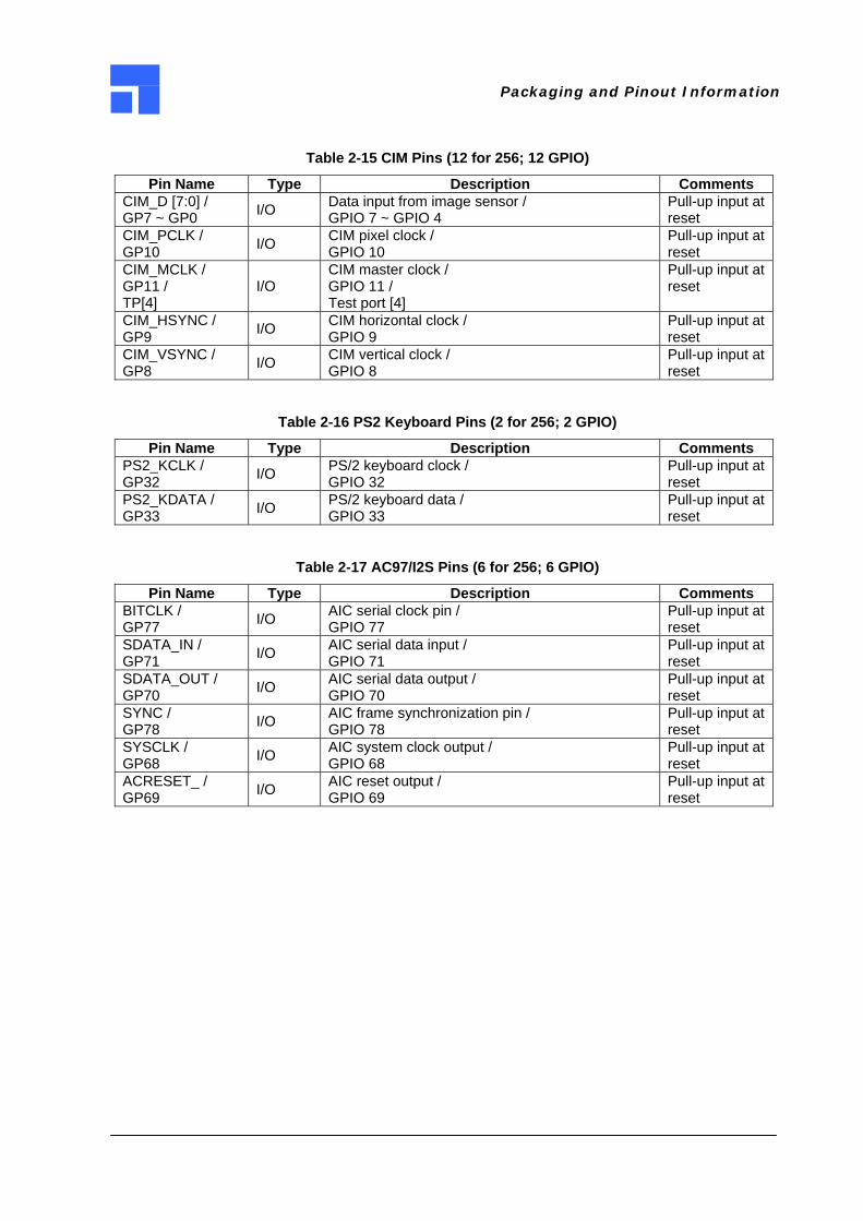
Table 2-15 CIM Pins (12 for 256; 12 GPIO)
Pin Name Type Description Comments CIM_D [7:0] / GP7 ~ GP0 I/O Data input from image sensor /
GPIO 7 ~ GPIO 4 Pull-up input at reset
CIM_PCLK / GP10 I/O CIM pixel clock /
GPIO 10 Pull-up input at reset
CIM_MCLK / GP11 / TP[4]
I/O CIM master clock / GPIO 11 / Test port [4]
Pull-up input at reset
CIM_HSYNC / GP9 I/O CIM horizontal clock /
GPIO 9 Pull-up input at reset
CIM_VSYNC / GP8 I/O CIM vertical clock /
GPIO 8 Pull-up input at reset
Table 2-16 PS2 Keyboard Pins (2 for 256; 2 GPIO)
Pin Name Type Description Comments PS2_KCLK / GP32 I/O PS/2 keyboard clock /
GPIO 32 Pull-up input at reset
PS2_KDATA / GP33 I/O PS/2 keyboard data /
GPIO 33 Pull-up input at reset
Table 2-17 AC97/I2S Pins (6 for 256; 6 GPIO)
Pin Name Type Description Comments BITCLK / GP77 I/O AIC serial clock pin /
GPIO 77 Pull-up input at reset
SDATA_IN / GP71 I/O AIC serial data input /
GPIO 71 Pull-up input at reset
SDATA_OUT / GP70 I/O AIC serial data output /
GPIO 70 Pull-up input at reset
SYNC / GP78 I/O AIC frame synchronization pin /
GPIO 78 Pull-up input at reset
SYSCLK / GP68 I/O AIC system clock output /
GPIO 68 Pull-up input at reset
ACRESET_ / GP69 I/O AIC reset output /
GPIO 69 Pull-up input at reset
Jz4730 Processor Data Book 13

Packaging and Pinout Information
Table 2-18 MSC Pins (6 for 256; 6 GPIO)
Pin Name Type Description Comments MSC_DAT[3] / GP37 I/O MSC data /
GPIO 37 Pull-up input at reset
MSC_DAT[2] / GP36 I/O MSC data /
GPIO 36 Pull-up input at reset
MSC_DAT[1] / GP35 I/O MSC data /
GPIO 35 Pull-up input at reset
MSC_DAT[0] / GP34 I/O MSC data /
GPIO 34 Pull-up input at reset
MSC_CMD / GP38 I/O MSC command /
GPIO 38 Pull-up input at reset
MSC_CLK / GP39 I/O MSC clock output /
GPIO 39 Pull-up input at reset
Table 2-19 GPIO Pins (15 for 256;)
Pin Name Type Description Comments
GP110 ~ GP96 I/O Special GPIO 110 ~ GPIO 96 Pull-up input at reset
Table 2-20 JTAG Pins (5 for 256)
Pin Name Type Description Comments
TRSTN_ Input JTAG reset Internal pull-down
TMS Input JTAG mode select Internal pull-upTDI Input JTAG serial data input Internal pull-up
TCK Input JTAG clock Internal pull-down
TDO Output JTAG serial data output
Jz4730 Processor Data Book 14

Packaging and Pinout Information
Table 2-21 System Pins (11 for 256)
Pin Name Type Description Comments
EXTAL Analog Input System clock input
XTAL Analog Output OSC output
RTCCLK Input RTC clock input RESETOUT_ Output Reset output RESETP_ Input System power on reset input
BOOT_SEL[3] Input Boot select input 3: 0->boot from ROM at CS0; 1->boot from NAND flash device at CS3
Internal pull-down
BOOT_SEL[2] Input
Boot select input 2: NAND flash address cycles when boot from it, 0->low cycle; 1->high cycle
Internal pull-down
BOOT_SEL[1] Input
Boot_select input 1: NAND flash page size when boot from it, 0->512B; 1->2048B
Internal pull-down
BOOT_SEL[0] Input
Boot select input 0: NAND flash width when boot from it, 0->8bit; 1->16bit
Internal pull-down
TEST_MODE Input Chip test mode Internal pull-down
TAP_MD Input TAP mode input - (1: internal JTAG; 0: boundary)
Internal pull-down
Table 2-22 Power Pins (28 for 256)
Pin Name Description VDD(IO1) Power supply for IO pad (1.8v) VSS(IO1) Ground supply for IO pad (0v) VDD(IO2) Power supply for IO pad (3.3v) VSS(IO2) Ground supply for IO pad (0v) VDD(core) Power supply for core (1.8v) VSS(core) Ground supply for core (0v) VDD(PLL) PLL power supply for analog (1.8v) VSS(PLL) PLL ground supply for analog VDD(USB) Power supply for USB IO pad (3.3v) VSS(USB) Ground supply for USB IO pad (0v)
Jz4730 Processor Data Book 15

Packaging and Pinout Information
2.3 Package Dimension
Jz4730 Processor Data Book 16

Packaging and Pinout Information
2.4 Ball Assignment
1 2 3 4 5 6 7 8 9 10 11 12 13 14 15 16 17 18 19 20 A B C D E F G H J K L M N P R T U V W Y
Figure 2-3 Jz4730 256-ball BGA Pinout (Top View)
Jz4730 Processor Data Book 17

Packaging and Pinout Information
Table 2-23 Ball Assignment
Ball # Signal Name Ball # Signal Name Ball # Signal Name A1 MII_TX_CLK E19 A[4] T17 NC A2 MII_MDC E20 A[5] T18 UART1_RXD A3 MII_RX_ER F1 LCD_D[6] T19 UART2_RXD A4 MII_RX_CLK F2 LCD_D[9] T20 UART1_TXD A5 AEN F3 LCD_D[11] U1 DPLS0 A6 VDD(IO1) F4 MII_TXD[2] U2 DMNS0 A7 CS5_ F17 A[6] U3 VSS(USB) A8 CS2_ F18 A[7] U4 NC A9 WAIT_ F19 A[8] U5 XTAL A10 A[0] F20 A[9] U6 TDO A11 A[18] G1 LCD_D[2] U7 TRSTN_ A12 A[22] G2 LCD_D[4] U8 SSI_DR A13 A[25] G3 LCD_D[8] U9 VDD(IO2) A14 CKO G4 VSS(IO2) U10 VSS(IO2) A15 WE0_ G17 A[10] U11 VDD(core) A16 D[2] G18 A[11] U12 VSS(core) A17 D[6] G19 A[12] U13 GP99 A18 D[9] G20 A[13] U14 GP108 A19 D[11] H1 LCD_PCLK U15 MSC_CMD A20 D[12] H2 LCD_D[1] U16 MSC_DAT[1] B1 MII_MDIO H3 LCD_D[5] U17 NC B2 MII_TXD1 H4 VDD(IO2) U18 UART3_TXD B3 MII_RXD2 H17 VSS(IO1) U19 UART3_RXD B4 MII_CRS H18 A[14] U20 UART0_RXD B5 DREQ0 H19 A[15] V1 VDD(USB) B6 DACK0 H20 A[16] V2 VSS(PLL) B7 FEW_ J1 LCD_VSYNC V3 NC B8 CS3_ J2 LCD_HSYNC V4 EXTAL B9 CS0_ J3 LCD_D[0] V5 I2C_SCK B10 RD_ J4 LCD_D[3] V6 TCK B11 A[17] J17 VDD(IO1) V7 BOOT_SEL[2] B12 A[21] J18 D[16] V8 SSI_CE1_ B13 A[24] J19 D[17] V9 SYSCLK B14 DCS0_ J20 D[18] V10 SYNC B15 RAS_ K1 LCD_CLS V11 PWM1 B16 D[1] K2 LCD_SPL V12 SCC0_DATA B17 D[5] K3 LCD_DE V13 GP103 B18 D[8] K4 VSS(core) V14 GP98 B19 D[10] K17 VDD(core) V15 GP109 B20 D[13] K18 D[19] V16 GP105 C1 LCD_D[14] K19 D[20] V17 MSC_DAT[3] C2 MII_TXD[0] K20 D[21] V18 UART3_RTS_ C3 MII_TXD[3] L1 LCD_PS V19 NC C4 MII_RXD[0] L2 LCD_REV V20 UART2_TXD C5 MII_RX_DV L3 TAP_MD W1 VDD(PLL) C6 EOP L4 VDD(core) W2 RTCCLK C7 FRE_ L17 VSS(core) W3 RESETP_ C8 CS4_ L18 D[22] W4 RESETOUT_ C9 CS1_ L19 D[23] W5 TDI C10 WE_ L20 D[24] W6 BOOT_SEL[0] C11 A[1] M1 CIM_D[0] W7 BOOT_SEL[1]
Jz4730 Processor Data Book 18

Packaging and Pinout Information
Table 2-24 Ball Assignment (continue)
Ball # Signal Name Ball # Signal Name Ball # Signal Name C12 A[20] M2 CIM_D[1] W8 SSI_DT C13 A[23] M3 CIM_D[2] W9 SDATA_OUT C14 DCS1_ M4 CIM_D[3] W10 ACRESET_ C15 CAS_ M17 D[25] W11 PS2_CLK C16 D[0] M18 D[26] W12 SCC0_CLK C17 D[4] M19 D[27] W13 SCC1_DATA C18 D[7] M20 D[28] W14 GP101 C19 D[14] N1 CIM_D[4] W15 GP97 C20 D[15] N2 CIM_D[5] W16 GP106 D1 LCD_D[10] N3 CIM_D[6] W17 GP104 D2 LCD_D[12] N4 CIM_D[7] W18 MSC_DAT[0] D3 MII_TX_EN N17 D[29] W19 NC D4 MII_RXD[1] N18 D[30] W20 UART3_CTS_ D5 MII_COL N19 D[31] Y1 NC D6 VSS(IO2) N20 IOIS16_ Y2 NC D7 FRB_ P1 CIM_MCLK Y3 NC D8 VDD(IO1) P2 CIM_PCLK Y4 I2C_SDA D9 VSS(IO1) P3 CIM_HSYNC Y5 TMS D10 VDD(core) P4 CIM_VSYNC Y6 BOOT_SEL[3] D11 VSS(core) P17 VSS(IO2) Y7 SSI_CE2_ D12 A[19] P18 PCE2_ Y8 SSI_CLK D13 VSS(IO1) P19 PCE1_ Y9 BITCLK D14 VDD(IO1) P20 PSKTSEL Y10 SDATA_IN D15 CKE R1 TEST_MD Y11 PWM0 D16 WE1_ R2 VDD(core) Y12 PS2_DATA D17 D[3] R3 USB_CLK Y13 SCC1_CLK D18 RDWR_ R4 VSS(core) Y14 GP102 D19 WE2_ R17 VDD(IO1) Y15 GP100 D20 WE3_ R18 INPACK_ Y16 GP96 E1 LCD_D[7] R19 PBVD2 Y17 GP110 E2 LCD_D[13] R20 UART0_TXD Y18 GP107 E3 LCD_D[15] T1 OVC0 Y19 MSC_CLK E4 MII_RXD[3] T2 PPWR0 Y20 MSC_DAT[2] E17 A[2] T3 DPLS1 E18 A[3] T4 DMNS1
2.5 Package Power Ratings
Table 2-24 θJA and Maximum Power Ratings
Processor θJA Max Power Jz4730 ??.? °C /w ?.??W
Jz4730 Processor Data Book 19

Packaging and Pinout Information
Chapter 3 Electrical Specifications
3.1 Absolute Maximum Ratings
This section provides the absolute maximum ratings for the processors. Do not exceed these parameters or the part may be damaged permanently. Operation at absolute maximum ratings is not guaranteed.
Table 3-1 Absolute Maximum Ratings
Symbol Description Min Max UnitTs Storage Temperature -40 125 °C VSS_O Offset Voltage between any two VSS pins -0.3 0.3 V
VDD_O Offset Voltage between any of the following pins: VDD(core), VDD(IO1), VDD(IO2) -0.3 0.3 V
VDD_HV Voltage Applied to High Voltage Supplies (VDD(IO2), VDD(USB)) VSS-0.3 VSS+4.0 V
VDD_LV Voltage Applied to Low Voltage Supplies (VDD(core), VDD(IO1), VDD(PLL)) VSS-0.3 VSS+2.5 V
VIP1 Voltage Applied to non-Supply pins VSS-0.3 max of ??? V
VIP2 Voltage Applied to non-Supply pins VSS-0.3max of
VDD(IO2)+0.3 VSS+4.0
V
VESD
Maximum ESD stress voltage, Human Body Model; Any pin to any supply pin, either polarity, or Any pin to all non-supply pins together, either polarity. Three stresses maximum.
2000 V
3.2 Power Consumption Specifications Power consumption depends on the operating voltage, peripherals enabled, external switching activity, and external loading. The maximum power consumption specification is determined by all units running at their maximum: processor speed, voltage, and loading conditions. This method generates a conservative power consumption value; however, power supply and thermal management design requires the highest possible power consumption for robust design. The Jz4730 processor’s maximum power consumption is calculated using the following conditions:
• All peripheral units operating at maximum frequency and size configuration
• All I/O loads maximum (50pF for Memory interface, 100pF for peripherals)
• Core operating at worst case power scenario (hit rates adjusted for worst power)
• All voltages at maximum of range
Do not exceed the maximum package power rating or Tcase temperature.
Jz4730 Processor Data Book 20

Packaging and Pinout Information
But for most of applications, a more optimal system design requires more typical power-consumption figures. These figures are important when considering battery size and optimizing regulator efficiency. Typical systems operate with fewer modules active and at nominal voltage and load. The typical power consumption for the Jz4730 processor is calculated using these conditions:
•
•
•
• All voltage at nominal value
• Nominal case temperature
Table 3-2 Power Consumption Specifications
Symbol Description Typical Max Unit400MHz normal mode; Maximum: V(core)= 2.2V, V(IO1)=V, V(IO2)=3.6V, Temp=100°C Typical: V(core)=1.8V, V(IO1)=1.8V, V(IO2)=3.3V, Temp=Room mW mW mW mW mW mW mW mW mW
Jz4730 Processor Data Book 21

Packaging and Pinout Information
3.3 Operating Conditions
This section shows voltage, frequency, and temperature specifications for the Jz4730 processor. The frequency range is operation voltage dependent.
Table 3-3 Voltage, Temperature, and Frequency Electrical Specifications
Symbol Description Min Typical Max Unit TA Ambient Temperature 0 – 70 °C VDD(core) Core Voltage 1.5 1.8 2.2 V VDD(IO1) IO Voltage ??? 1.8 ??? V VDD(IO2) IO Voltage 3.0 3.3 3.6 V VDD(PLL) PLL Analog Voltage 1.5 1.8 2.2 V VDD(USB) USB Analog Voltage 3.0 3.3 3.6 V VSS(core) Core Power Ground 0 V VSS(IO1) IO Power Ground 0 V VSS(IO2) IO Power Ground 0 V VSS(PLL) PLL Power Ground 0 V VSS(USB) USB Power Ground 0 V Low Voltage Range VDD(core) Core Voltage 1.5 V VDD(PLL) PLL Analog Voltage 1.5 V FCORE CPU Core Frequency MHz FSDARM SDRAM Frequency MHz Medium Voltage Range VDD(core) Core Voltage 1.8 V VDD(PLL) PLL Analog Voltage 1.8 V FCORE CPU Core Frequency MHz FSDARM SDRAM Frequency MHz High Voltage Range VDD(core) Core Voltage 2.2 V VDD(PLL) PLL Analog Voltage 2.2 V FCORE CPU Core Frequency MHz FSDARM SDRAM Frequency MHz
3.4 DC Specifications The DC characteristics for each pin include input-sense levels and output-drive levels and currents. These parameters can be used to determine maximum DC loading, and also to determine maximum transition times for a given load. The output and I/O pin categories are list in Table 3-4. The DC Operating Conditions for Input, Output, and I/O pins are shown in Table 3-5, All DC specification values are valid for the entire temperature range of the device.
Table 3-4 Categories for Output, and I/O Pins
Category Name Pins Description
G12 A[16:2], RDWR_, CKOx SDRAM signals G8 D[31:0], RAS_, CAS_, CKE, DCS0_, DCS1_, WEx_ SDRAM signals and …
G4 FRB_, IOIS16_, PSKTSEL, PCE1_, PCE2_, LCD_D[15:0], LCD_VSYNC, LCD_HSYNC, LCD_PCLK, LCD_DE, LCD_SPL, LCD_CLS, LCD_PS, LCD_REV,
PCMCIA, LCD, I2C, SCC, PWM, MSC, special GPIO, and …
Jz4730 Processor Data Book 22

Packaging and Pinout Information
I2C_SDA, I2C_SCK, SCC0_DATA, SCC0_CLK, SCC1_DATA, SCC1_CLK, PWM0, PWM1, MSC_DAT[3:0], MSC_CMD, MSC_CLK, GP110~GP96, TDO, RESETOUT_
G2 All other output, I/O pins except XTAL(1), D+/D-(2) of UHC and power supply pins
NOTE: (1) See 错误!未找到引用源。 for XTAL (2) UHC D+/D- signals compliant USB 1.1 standard
Table 3-5 Standard Input, Output, and I/O Pin DC Operating Conditions
Symbol Description Min Typical Max UnitInput DC Operating Conditions
VIH Input High Voltage, all standard input and I/O pins
0.8 * VDD(IO2) 5.5 V
VIL Input Low Voltage, all standard input and I/O pins VSS 0.2 *
VDD(IO2) V
IIN Input Leakage, all standard input and IO pins 10 uA
Output DC Operating Conditions
VOH Output High Voltage, all standard output and I/O pins
VDDIO – 0.6 VDDIO V
VOL Output Low Voltage, all standard output and I/O pins VSS VSS + 0.4 V
IOH_G12 Output High Current, GP pins (VO=VOH) 12 mA IOL_G12 Output Low Current, GP pins (VO=VOH) 12 mA IOH_G8 Output High Current, GP pins (VO=VOH) 8 mA IOL_G8 Output Low Current, GP pins (VO=VOH) 8 mA IOH_G4 Output High Current, GP pins (VO=VOH) 4 mA IOL_G4 Output Low Current, GP pins (VO=VOH) 4 mA IOH_G2 Output High Current, GP pins (VO=VOH) 2 mA IOL_G2 Output Low Current, GP pins (VO=VOH) 2 mA
Table 3-6 Standard Input, Output, and I/O Pin DC Operating Conditions for 1.8v Memory
Symbol Description Min Typical Max UnitInput DC Operating Conditions
VIH Input High Voltage, all standard input and I/O pins V
VIL Input Low Voltage, all standard input and I/O pins V
IIN Input Leakage, all standard input and IO pins uA
Output DC Operating Conditions
VOH Output High Voltage, all standard output and I/O pins V
VOL Output Low Voltage, all standard output and I/O pins V
Jz4730 Processor Data Book 23

Packaging and Pinout Information
3.5 AC Specifications A pin’s AC Characteristics include input and output capacitance. These determine loading for external drivers or other load analysis. The AC Characteristics also include a de-rating factor, which indicates how much faster or slower the AC timings get with different loads. The AC Operating Conditions for all input, output, and I/O pins are shown in Table 3-7. All AC specification values are valid for entire temperature range of the device.
Table 3-7 Standard Input, Output, and I/O Pin AC Operating Conditions
Symbol Description Min Typical Max UnitsCIN Input Capacitance, all input and IO pins 3 5 10 pF COUT_G12 Output Capacitance, G12 output and IO pins 5 – 120 pF
COUT_G8 Output Capacitance, G8 SDRAM output and IO pins 5 – 100 pF
NOTE: AC Specifications guaranteed for loads in this range. All testing is done at 50pF
3.6 Oscillator Electrical Specifications The processor contains two oscillators, each for a specific crystal: a 32.768KHz oscillator and a 3.6864MHz oscillator. When choosing a crystal, match the crystal parameters as closely as possible.
3.6.1 32.768KHz Oscillator Specifications
3.6.2 3.6864MHz Oscillator Specifications
3.7 Reset and Power AC Timing Specifications
The Jz4730 processor asserts the RESETOUT_ pin in one of several modes:
• Power On
• Power On Reset (RESETP_)
• Watch Dog Reset (internal controlled)
The following sections provide the timing and specifications for the entry and exit of these modes.
Jz4730 Processor Data Book 24

Packaging and Pinout Information
3.7.1 Power-On Timing The external voltage regulator and other power-on devices must provide the Jz4730 processor with a specific sequence of power and resets to ensure proper operation. ???, shows this sequence and is detailed in ???. On the processor, it is important that the power supplies be powered up in a certain order to avoid high current situations. The required order is:
1. VDD(IO2) & VDD(USB)
2. VDD(IO1)
3. VDDCORE & VDD(PLL)
tD_RESETP_
VDD(IO2)/VDD(USB)
tr_VDDIO2
VDD(core)/VDD(PLL)
tr_VDDCORE
RESETP_
tD_VDDCORE
tr_VDDIO1
tD_VDDIO VDD(IO1)
RESETOUT_ tD_RESETOUT_
JTAG PINS
tD_TRST_
TRST_ tD_JTAG
Figure 3-1 Power-On Timing Diagram
Table 3-8 Power-On Timing Parameters
Symbol Description Min Typical Max Unittr_VDDIO1, tr_VDDIO2
VDDIO/VDD(USB) Rise / Stabilization time 0.01 – 100 ms
tD_VDDIO Delay between VDDIO2/VDD(USB) stable and VDDIO1 applied 0 – – ms
tD_VDDCORE Delay between VDDIO/VDD(USB) stable and VDDCORE/VDD(PLL) applied 0 – – ms
tr_VDDOCRE VDDOCRE/VDD(PLL) Rise / Stabilization 0.01 – 100 ms
Jz4730 Processor Data Book 25

Packaging and Pinout Information
time
tD_TRST_ Delay between VDDCORE, VDD(PLL) stable and JTAG reset TRST_ deasserted 10 – – ns
tD_JTAG Delay between TRST_ deasserted and other JATG pins active 10 – – ns
tD_RESETP_ Delay between VDDCORE, VDD(PLL) stable and RESETP_ deasserted 0.2(1) – – ms
tD_RESETOU
T_ Delay between RESETP_ deasserted and RESETOUT_ deasserted 117.2 – 117.3 ms
3.7.2 Hardware Reset Timing
The timing sequences for input signals RESETP_ and output signals RESETOUT_, are shown in Figure 3-2 and Table 3-9, assumes the power supplies are stable at the assertion of RESETP_.
t fd_resetout_
RESETP_
RESETOUT_
t ac_reset_
t rd_resetout_
Figure 3-2 Hardware Reset Timing Diagram
Table 3-9 RESETP_ to RESETOUT_ Timing Parameters
Symbol Description Min Typical Max Unit tac_RESETP_ Minimum assertion time of RESETP_ 0.2(1) – – ms
tfd_RESETOUT_ Delay between RESETP_ Asserted and RESETOUT_ Asserted 3 7 20 ns
trd_RESETOUT_ Delay between RESETP_ deasserted and RESETOUT_ deasserted 117.2 – 117.3 ms
3.8 Memory Bus and PCMCIA AC Specifications This section provides the timing information for these types of memory:
• SRAM / ROM / Flash
Jz4730 Processor Data Book 26

Packaging and Pinout Information
• Card interface (PCMCIA or Compact Flash)
• SDRAM
3.9 Peripheral Module AC Specifications
3.9.1 LCD Module Timing
3.9.2 CIM Module Timing
3.9.3 SPI Module Timing
3.9.4 External DMA Request and Grant
Jz4730 Processor Data Book 27