data sheet sky77318 ipac™ pam for quad-band … module consists of separate gsm pa and...
TRANSCRIPT

Skyworks Solutions, Inc. • Phone [781] 376-3000 • Fax [781] 376-3100 • [email protected] • www.skyworksinc.com 200424B • Skyworks Proprietary and Confidential Information • Products and product information are subject to change without notice. • December 17, 2007 1
DATA SHEET
SKY77318 iPAC™ PAM for Quad-Band GSM / GPRSApplications
• Quad-Band cellular handsets encompassing - Class 4 GSM850/900 - Class 1 DCS1800/
PCS1900 - Class 12 GPRS multi-slot
operation
Features
• Low input power range - 0 to 6 dBm
• High efficiency - CELL 58% - GSM 56% - DCS 56% - PCS 56%
• BiCMOS PA controller and interface IC - Low power control slope - Fast response time - Improved control
accuracy
• Integrated closed loop power amplifier control
• Internal ICC sense resistor for PAC
• Input/Output matching 50 Ω internal (with DC blocking)
• 20-pad package
• Small outline: 6 x 6 mm
• Low profile: 1.2 mm
• MSL3/260 °C
Description The SKY77318 Power Amplifier Module (PAM) is designed in a low profile (1.2 mm), compact form factor for quad-band cellular handsets comprising GSM850/900, DCS1800, and PCS1900 operation. The PAM also supports Class 12 General Packet Radio Service (GPRS) multi-slot operation.
The module consists of separate GSM PA and DCS1800/PCS1900 PA blocks, impedance-matching circuitry for 50 Ω input and output impedances and a Power Amplifier Control (PAC) block with an internal current-sense resistor. The custom BiCMOS integrated circuit provides the internal PAC function and interface circuitry. Fabricated onto a single Gallium Arsenide (GaAs) die, one Heterojunction Bipolar Transistor (HBT) PA block supports the GSM bands and the other supports the DCS1800 and PCS1900 bands. Both PA blocks share common power supply pads to distribute current. The GaAs die, the Silicon (Si) die, and the passive components are mounted on a multi-layer laminate substrate. The assembly is encapsulated with plastic overmold.
RF input and output ports of the SKY77318 are internally matched to a 50 Ω load to reduce the number of external components for a quad-band design. Extremely low leakage current (2.5 μA, typical) of the dual PA module maximizes handset standby time. The SKY77318 also contains band-select switching circuitry to select GSM (logic 0) or DCS/PCS (logic 1) as determined from the Band Select (BS) signal. In Figure 1 below, the BS pad selects the PA output (DCS/PCS_OUT or GSM_OUT) and the Analog Power Control (VAPC) controls the level of output power.
The VBATT pad connects to an internal current-sense resistor and interfaces to an integrated power amplifier control (iPAC™) function, which is insensitive to variations in temperature, power supply, process, and input power. The ENABLE input allows initial turn-on of PAM circuitry to minimize battery drain.
200242_001
ENABLE
GSM_IN
BAND SELECT
VCC1
DCS/PCS_OUT
GSM_OUT
DCS/PCS_IN
VBATT
POWER CONTROL VAPC
GND
Match
Match
Match
MODULE
HBT
Match
BiCMOSIntegrated
PowerAmplifierController
PA
PA
Figure 1. Functional Block Diagram

DATA SHEET SKY77318 iPAC™ PAM FOR QUAD-BAND GSM / GPRS
Skyworks Solutions, Inc. • Phone [781] 376-3000 • Fax [781] 376-3100 • [email protected] • www.skyworksinc.com 2 December 17, 2007 • Skyworks Proprietary and Confidential Information. • Products and product information are subject to change without notice. • 200424B
Electrical SpecificationsThe following tables list the electrical characteristics of the SKY77318 Power Amplifier Module. Table 1 lists the absolute maximum ratings and Table 2 shows the recommended operating conditions. Table 3 lists the electrical characteristics of the SKY77318 for modes GSM, DCS1800, and PCS1900. Figure 2 is a diagram of a typical SKY77318 application.
The SKY77318 is a static-sensitive electronic device and should not be stored or operated near strong electrostatic fields. Detailed information on device dimensions, pad descriptions, packaging and handling can be found in later sections of this data sheet.
Table 1. Absolute Maximum Ratings
Parameter Minimum Maximum Unit
Input Power (PIN) — 15 dBm
Supply Voltage (VCC), Standby, VAPC ≤ 0.3 V, ENABLE ≤ 0.2 V
— 7 V
Control Voltage (VAPC) –0.5 VCC_MAX – 0.2 (See Table 3)
V
Storage Temperature –55 +150 °C
Table 2. Recommended Operating Conditions
Parameter Minimum Typical Maximum Unit
Supply Voltage (VCC) 2.9 3.5 4.8 V
Supply Current (ICC) 0 — 2.5 A
Operating Case Temperature (TCASE) – Package Bottom Surface
1-Slot (12.5% duty cycle) –20 — +100
2-Slot (25.0% duty cycle) –20 — +100
3-Slot (37.5% duty cycle) –20 — +85
4-Slot (50.0% duty cycle) –20 — +85
°C
Table 3. SKY77318 Electrical Specifications (1 of 9)
General
Parameter Symbol Test Condition Minimum Typical Maximum Units
Supply voltage VCC — 2.9 3.5 4.8 V
Power control impedance ZAPC — — 200 — kΩ
Low VPE — –0.1 — 0.6 ENABLE control voltage
High VPE — 1.2 — Vcc V
ENABLE current IPE VPE ≤ 3.0 V — — 30 μA
Low VBS — –0.1 — 0.6 V Band Select control voltage
High VBS — 1.2 — Vcc
Band Select current IBS VBS ≤ 3.0 V — — 30 μA
Standby Mode Leakage current IQ
VCC ≤ 4.5 V VAPC = 0.1 V ENABLE ≤ 0.2 V TCASE = +25 °C PIN ≤ –60 dBm
— 2.5 10 μA
VAPC Input Filter Bandwidth VAPC _FBW — 85 120 150 kHz
VAPC Threshold VAPC _THCL — 100 150 200 mV

SKY77318 iPAC™ PAM FOR QUAD-BAND GSM / GPRS DATA SHEET
Skyworks Solutions, Inc. • Phone [781] 376-3000 • Fax [781] 376-3100 • [email protected] • www.skyworksinc.com 200424B • Skyworks Proprietary and Confidential Information • Products and product information are subject to change without notice. • December 17, 2007 3
Table 3. SKY77318 Electrical Specifications 1 (2 of 9)
GSM850 Mode (f = 824 to 849 MHz and PIN = 0 to 6 dBm)
Parameter Symbol Test Condition Minimum Typical Maximum Units
Frequency range f — 824 — 849 MHz
Input power PIN — 0 — 6 dBm
Analog power control voltage VAPC — 0.2 — 1.7 V
Power Added Efficiency PAE
VCC = 3.5 V POUT = 34.75 dBm ENABLE > 2.0 V pulse width 577 μs duty cycle 1:8 TCASE = +25 °C
50 58 — %
2nd to 13th harmonics 2f0 to 13f0 BW = 3 MHz 6.5 dBm ≤ Pout ≤ 34.75 dBm
— — –10 dBm
POUT_MAX VCC = 3.5 V TCASE = +25 °C
34.75 35.2 —
POUT_MAX LOW VOLTAGE
VCC = 2.9 V ENABLE > 2.0 V TCASE = –20 °C to +100 °C (See Table 2 for multi-slot.) PIN = 0 dBm
32.5 — —
Output power
POUT_MAX HIGH VOLTAGE
VCC = 4.5 V ENABLE > 2.0 V TCASE = –20 °C to +100 °C (See Table 2 for multi-slot.) PIN = 0 dBm
32.5 — —
dBm
Input VSWR ΓIN POUT = 6.5 to 34.75 dBm, controlled by VAPC
— 1.5:1 2.5:1 —
Forward isolation POUT_STANDBY PIN = 6 dBm VAPC = 0.1 V ENABLE ≤ 0.2 V
— — –35 dBm
Spurious Spur
All combinations of the following parameters: VAPC = controlled 2 PIN = min. to max. VCC = 2.9 V to 4.8 V Load VSWR = 8:1, all phase angles
No parasitic oscillation > –36 dBm
DATA SHEET SKY77318 iPAC™ PAM FOR QUAD-BAND GSM / GPRS
Skyworks Solutions, Inc. • Phone [781] 376-3000 • Fax [781] 376-3100 • [email protected] • www.skyworksinc.com 4 December 17, 2007 • Skyworks Proprietary and Confidential Information. • Products and product information are subject to change without notice. • 200424B
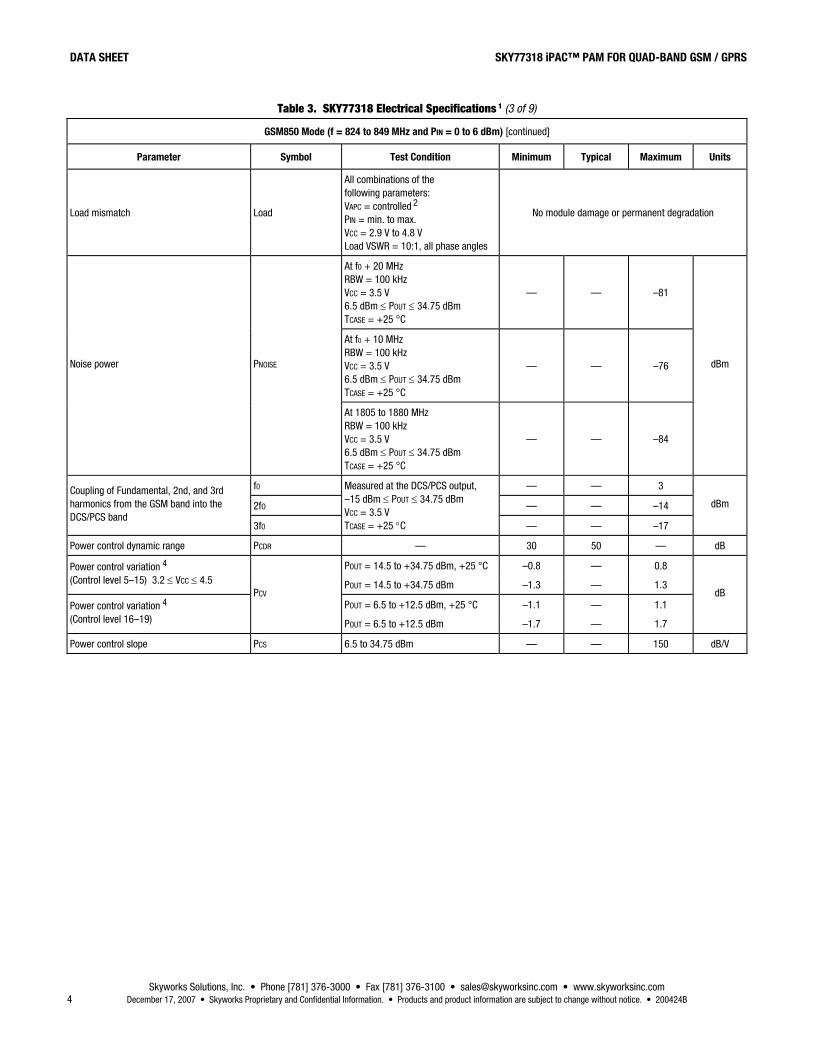
Table 3. SKY77318 Electrical Specifications 1 (3 of 9)
GSM850 Mode (f = 824 to 849 MHz and PIN = 0 to 6 dBm) [continued]
Parameter Symbol Test Condition Minimum Typical Maximum Units
Load mismatch Load
All combinations of the following parameters: VAPC = controlled 2 PIN = min. to max. VCC = 2.9 V to 4.8 V Load VSWR = 10:1, all phase angles
No module damage or permanent degradation
At f0 + 20 MHz RBW = 100 kHz VCC = 3.5 V 6.5 dBm ≤ POUT ≤ 34.75 dBm TCASE = +25 °C
— — –81
At fO + 10 MHz RBW = 100 kHz VCC = 3.5 V 6.5 dBm ≤ POUT ≤ 34.75 dBm TCASE = +25 °C
— — –76 Noise power PNOISE
At 1805 to 1880 MHz RBW = 100 kHz VCC = 3.5 V 6.5 dBm ≤ POUT ≤ 34.75 dBm TCASE = +25 °C
— — –84
dBm
f0 — — 3
2fO — — –14
Coupling of Fundamental, 2nd, and 3rd harmonics from the GSM band into the DCS/PCS band
3f0
Measured at the DCS/PCS output, –15 dBm ≤ POUT ≤ 34.75 dBm VCC = 3.5 V TCASE = +25 °C — — –17
dBm
Power control dynamic range PCDR — 30 50 — dB
POUT = 14.5 to +34.75 dBm, +25 °C –0.8 — 0.8 Power control variation 4 (Control level 5–15) 3.2 ≤ VCC ≤ 4.5 POUT = 14.5 to +34.75 dBm –1.3 — 1.3
POUT = 6.5 to +12.5 dBm, +25 °C –1.1 — 1.1 Power control variation 4 (Control level 16–19)
PCV
POUT = 6.5 to +12.5 dBm –1.7 — 1.7
dB
Power control slope PCS 6.5 to 34.75 dBm — — 150 dB/V

SKY77318 iPAC™ PAM FOR QUAD-BAND GSM / GPRS DATA SHEET
Skyworks Solutions, Inc. • Phone [781] 376-3000 • Fax [781] 376-3100 • [email protected] • www.skyworksinc.com 200424B • Skyworks Proprietary and Confidential Information • Products and product information are subject to change without notice. • December 17, 2007 5
Table 3. SKY77318 Electrical Specifications 1 (4 of 9)
GSM900 Mode (f = 880 to 915 MHz and PIN = 0 to 6 dBm)
Parameter Symbol Test Condition Minimum Typical Maximum Units
Frequency range f — 880 — 915 MHz
Input power PIN — 0 — 6 dBm
Analog power control voltage VAPC — 0.2 — 1.7 V
Power Added Efficiency PAE
VCC = 3.5 V POUT = 34.5 dBm ENABLE > 2.0 V pulse width 577 μs duty cycle 1:8 TCASE = +25 °C
48 56 — %
2f0 to 13f0 — — –10 2nd to 13th harmonics
7F0
BW = 3 MHz 6.5 dBm ≤ POUT ≤ 34.5 dBm TCASE = +25 °C — — –5
dBm
POUT_MAX VCC = 3.5 V TCASE = +25 °C
34.5 35.2 —
POUT_MAX LOW VOLTAGE
VCC = 2.9 V ENABLE > 2.0 V TCASE = –20 °C to +100 °C (See Table 2 for multi-slot.) PIN = 0 dBm
32.5 — —
Output power
POUT_MAX HIGH VOLTAGE
VCC = 4.5 V ENABLE > 2.0 V TCASE = –20 °C to +100 °C (See Table 2 for multi-slot.) PIN = 0 dBm
32.5 — —
dBm
Input VSWR ΓIN POUT = 6.5 to 34.5 dBm, controlled by VAPC
— 1.5:1 2.5:1 —
Forward isolation POUT_STANDBY PIN = 6 dBm VAPC = 0.1 V ENABLE ≤ 0.2 V
— — –35 dBm
Spurious Spur
All combinations of the following parameters: VAPC = controlled 2 PIN = min. to max. VCC = 2.9 V to 4.8 V Load VSWR = 8:1, all phase angles
No parasitic oscillation > –36 dBm

DATA SHEET SKY77318 iPAC™ PAM FOR QUAD-BAND GSM / GPRS
Skyworks Solutions, Inc. • Phone [781] 376-3000 • Fax [781] 376-3100 • [email protected] • www.skyworksinc.com 6 December 17, 2007 • Skyworks Proprietary and Confidential Information. • Products and product information are subject to change without notice. • 200424B
Table 3. SKY77318 Electrical Specifications 1 (5 of 9)
GSM900 Mode (f = 880 to 915 MHz and PIN = 0 to 6 dBm) [continued]
Parameter Symbol Test Condition Minimum Typical Maximum Units
Load mismatch Load
All combinations of the following parameters: VAPC = controlled 2 PIN = min. to max. VCC = 2.9 V to 4.8 V Load VSWR = 10:1, all phase angles
No module damage or permanent degradation
At f0 + 20 MHz RBW = 100 kHz VCC = 3.5 V 6.5 dBm ≤ POUT ≤ 34.75 dBm TCASE = +25 °C
— — –81
At f0 + 10 MHz RBW = 100 kHz VCC = 3.5 V 6.5 dBm ≤ POUT ≤ 34.75 dBm TCASE = +25 °C
— — –76 Noise power PNOISE
At 1805 to 1880 MHz RBW = 100 kHz VCC = 3.5 V 6.5 dBm ≤ POUT ≤ 34.75 dBm TCASE = +25 °C
— — –84
dBm
f0 — — 3
2fO — — –16
Coupling of Fundamental, 2nd, and 3rd harmonics from the GSM band into the DCS/PCS band
3f0
Measured at the DCS/PCS output, –15 dBm ≤ POUT ≤ 34.75 dBm VCC = 3.5 V TCASE = +25 °C — — –17
dBm
Power control dynamic range PCDR — 30 50 — dB
POUT = 14.5 to +34.75 dBm, +25 °C –0.8 — 0.8 Power control variation 4 (Control level 5–15) 3.2 ≤ VCC ≤ 4.5 POUT = 14.5 to +34.75 dBm –1.3 — 1.3
POUT = 6.5 to +12.5 dBm, +25 °C –1.1 — 1.1 Power control variation 4 (Control level 16–19)
PCV
POUT = 6.5 to +12.5 dBm –1.7 — 1.7
dB
Power control slope PCS 6.5 to 34.75 dBm — — 150 dB/V

SKY77318 iPAC™ PAM FOR QUAD-BAND GSM / GPRS DATA SHEET
Skyworks Solutions, Inc. • Phone [781] 376-3000 • Fax [781] 376-3100 • [email protected] • www.skyworksinc.com 200424B • Skyworks Proprietary and Confidential Information • Products and product information are subject to change without notice. • December 17, 2007 7
Table 3. SKY77318 Electrical Specifications 1 (6 of 9)
DCS1800 Mode (f = 1710 to 1785 MHz and PIN = 0 to 6 dBm)
Parameter Symbol Test Condition Minimum Typical Maximum Units
Frequency range f — 1710 — 1785 MHz
Input power PIN — 0 — 6 dBm
Analog power control voltage VAPC — 0.2 — 1.7 V
Power Added Efficiency PAE
VCC = 3.5 V POUT = 32.8 dBm ENABLE > 2.0 V pulse width 577 μs duty cycle 1:8 TCASE = +25 °C
48 52 — %
2nd to 7th harmonics 2f0 to 7f0
BW = 3 MHz 1.5 dBm ≤ POUT ≤ 32.8 dBm VCC = 3.5 V TCASE = +25 °C
— — –10 dBm
POUT_MAX VCC = 3.5 V TCASE = +25 °C
32.8 33.5 —
POUT_MAX LOW VOLTAGE
VCC = 2.9 V ENABLE > 2.0 V TCASE = –20 °C to +100 °C (See Table 2 for multi-slot.) PIN = 0 dBm
30.0 — —
Output power
POUT_MAX HIGH VOLTAGE
VCC = 4.5 V ENABLE > 2.0 V TCASE = –20 °C to +100 °C (See Table 2 for multi-slot.) PIN = 0 dBm
30.0 — —
dBm
Input VSWR ΓIN POUT = 1.5 to 32.8 dBm, controlled by VAPC
— 1.5:1 2.5:1 —
Forward isolation POUT_STANDBY PIN = 6 dBm VAPC = 0.1 V ENABLE ≤ 0.2 V
— — –35 dBm
Spurious Spur
All combinations of the following parameters: VAPC = controlled 3 PIN = min. to max. VCC = 2.9 V to 4.8 V Load VSWR = 8:1, all phase angles
No parasitic oscillation > –36 dBm

DATA SHEET SKY77318 iPAC™ PAM FOR QUAD-BAND GSM / GPRS
Skyworks Solutions, Inc. • Phone [781] 376-3000 • Fax [781] 376-3100 • [email protected] • www.skyworksinc.com 8 December 17, 2007 • Skyworks Proprietary and Confidential Information. • Products and product information are subject to change without notice. • 200424B
Table 3. SKY77318 Electrical Specifications 1 (7 of 9)
DCS1800 Mode (f = 1710 to 1785 MHz and PIN = 0 to 6 dBm) [continued]
Parameter Symbol Test Condition Minimum Typical Maximum Units
Load mismatch Load
All combinations of the following parameters: VAPC = controlled 3 PIN = min. to max. VCC = 2.9 V to 4.8 V Load VSWR = 10:1, all phase angles
No module damage or permanent degradation
At f0 + 20 MHz RBW = 100 kHz VCC = 3.5 V 1.5 dBm ≤ POUT ≤ 32.8 dBm TCASE = +25 °C
— — –78
Noise power PNOISE At 925 to 960 MHz RBW = 100 kHz VCC = 3.5 V 1.5 dBm ≤ POUT ≤ 32.8 dBm TCASE = +25 °C
— — –87
dBm
Power control dynamic range PCDR — 35 50 — dB
POUT = 15.5 to +32.8 dBm, +25 °C –1.1 — 1.1 Power control variation 4 (Control level 0–8) 3.2 V ≤ VCC ≤ 4.5 V POUT = 15.5 to +32.8 dBm –2.0 — 1.2
POUT = 5.5 to +13.5 dBm, +25 °C –1.1 — 1.1 Power control variation 4 (Control level 9–13) POUT = 5.5 to +13.5 dBm –3.4 — 1.4
POUT = 1.5 to +3.5 dBm, +25 °C –1.4 — 0.8 Power control variation 4 (Control level 14–15)
PCV
POUT = 1.5 to +3.5 dBm –4.0 — 2.0
dB
Power control slope PCS 1.5 to 32.8 dBm — — 150 dB/V

SKY77318 iPAC™ PAM FOR QUAD-BAND GSM / GPRS DATA SHEET
Skyworks Solutions, Inc. • Phone [781] 376-3000 • Fax [781] 376-3100 • [email protected] • www.skyworksinc.com 200424B • Skyworks Proprietary and Confidential Information • Products and product information are subject to change without notice. • December 17, 2007 9
Table 3. SKY77318 Electrical Specifications 1 (8 of 9)
PCS1900 Mode (f = 1850 to 1910 MHz and PIN = 0 to 6 dBm)
Parameter Symbol Test Condition Minimum Typical Maximum Units
Frequency range F — 1850 — 1910 MHz
Input power PIN — 0 — 6 dBm
Analog power control voltage VAPC — 0.2 1.7 V
Power Added Efficiency PAE
VCC = 3.5 V POUT = 32.8 dBm ENABLE > 2.0 V pulse width 577 μs duty cycle 1:8 TCASE = +25 °C
48 52 — %
2f0 to 7f0 — — –10
2nd to 7th harmonics 5f0
BW = 3 MHz 1.5 dBm ≤ POUT ≤ 32.8 dBm VCC = 3.5 V TCASE = +25 °C
— — –7 dBm
POUT_MAX VCC = 3.5 V TCASE = +25 °C
32.8 33.5 —
POUT_MAX LOW VOLTAGE
VCC = 2.9 V ENABLE > 2.0 V TCASE = –20 °C to +100 °C (See Table 2 for multi-slot.) PIN = 0 dBm
30.0 — —
Output power
POUT_MAX HIGH VOLTAGE
VCC = 4.5 V ENABLE > 2.0 V TCASE = –20 °C to +100 °C (See Table 2 for multi-slot.) PIN = 0 dBm
30.0 — —
dBm
Input VSWR ΓIN POUT = 1.5 to 32.8 dBm, controlled by VAPC
— 1.5:1 2.5:1 —
Forward isolation POUT_STANDBY PIN = 6 dBm VAPC = 0.1 V ENABLE ≤ 0.2 V
— — –35 dBm
Spurious Spur
All combinations of the following parameters: VAPC = controlled 3 PIN = min. to max. VCC = 2.9 V to 4.8 V Load VSWR = 8:1, phase angles
No parasitic oscillation > –36 dBm

DATA SHEET SKY77318 iPAC™ PAM FOR QUAD-BAND GSM / GPRS
Skyworks Solutions, Inc. • Phone [781] 376-3000 • Fax [781] 376-3100 • [email protected] • www.skyworksinc.com 10 December 17, 2007 • Skyworks Proprietary and Confidential Information. • Products and product information are subject to change without notice. • 200424B
Table 3. SKY77318 Electrical Specifications 1 (9 of 9)
PCS1900 Mode (f = 1850 to 1910 MHz and PIN = 0 to 6 dBm) [continued]
Parameter Symbol Test Condition Minimum Typical Maximum Units
Load mismatch Load
All combinations of the following parameters: VAPC = controlled 3 PIN = min. to max. VCC = 2.9 V to 4.8 V Load VSWR = 10:1, all phase angles
No module damage or permanent degradation
At f0 + 20 MHz RBW = 100 kHz VCC = 3.5 V 1.5 dBm ≤ POUT ≤ 32.8 dBm TCASE = +25 °C
— — –78
Noise power PNOISE At 880 to 915 MHz RBW = 100 kHz VCC = 3.5 V 1.5 dBm ≤ POUT ≤ 32.8 dBm TCASE = +25 °C
— — –87
dBm
Power control dynamic range PCDR — 35 50 — dB
POUT = 15.5 to +32.8 dBm, +25 °C –1.1 — 1.1 Power control variation 4 (Control level 0–8) 3.2 V ≤ VCC ≤ 4.5 V
PCV POUT = 15.5 to +32.8 dBm –2.0 — 1.2
dB
POUT = 5.5 to +13.5 dBm, +25 °C –1.1 — 1.1 Power control variation 4 (Control level 9–13)
PCV POUT = 5.5 to +13.5 dBm –3.4 — 1.4
dB
POUT = 1.5 to +3.5 dBm, +25 °C –1.4 — 0.8 Power control variation 4 (Control level 14–15)
PCV POUT = 1.5 to +3.5 dBm –4.0 — 2.0
dB
Power control slope PCS 1.5 to 32.8 dBm — — 150 dB/V
1 Unless specified otherwise: TCASE = –20 °C to max. operating temperature (see Table 2) RL = 50 Ω pulsed operation with pulse width ≤ 1154 μs and duty cycle ≤ 2:8 VCC = 2.9 V to 4.8 V.
2 ICC = 0A to xA, where x = current at POUT = 34.75 dBm for Cell and 34.5 dBm for GSM, 50 Ω load, and VCC = 3.5 V. 3 ICC = 0A to xA, where x = current at POUT = 32.8 dBm, 50 Ω load, and VCC = 3.5 V. 4 Power control variation is measured by comparing power obtained at a specified control voltage over all conditions, against the power obtained with the same control voltage at nominal
conditions. For this module, nominal conditions are defined as: T = 25 °C VCC = 3.5 V PIN = 3 dBm Frequency = mid-band

SKY77318 iPAC™ PAM FOR QUAD-BAND GSM / GPRS DATA SHEET
Skyworks Solutions, Inc. • Phone [781] 376-3000 • Fax [781] 376-3100 • [email protected] • www.skyworksinc.com 200424B • Skyworks Proprietary and Confidential Information • Products and product information are subject to change without notice. • December 17, 2007 11
200424_002
20 7
1 2 43 5 6
1017
16 15 1314 12 11
8
918
19
SKY77318
From Battery
0.01μF
0402
33 μF
0.01μF
BS
0.01μF
VCC1AVCC1A
VCC1B
GND
GND
GSM_INDCS/PCS_IN
VAPC
RSVD(GND)
ENABLE
VBATT
GND DCS/PCS_OUT GND GND GSM_OUT
GND
GND
GND
GND
Place 0402 and 33 μF caps as close as possible to theVBATT pin with the 0402
closer to the pin.
DC Supply trace to VCC1 must not be routed via VBATT pin 17.
NOTES:1. The value of 33 μF cap depends on the noise level on the phone board.2. Depending on phone board noise level, not all 0402 and 0.01 μF caps may be needed.3. Ensure sufficient numbers of vias connect VBATT pin to battery trace.4. VBATT trace should be ≥ 1.0 mm.5. Ensure sufficient numbers of vias connect VCC1A and B to battery trace.6. VCC1A and VCC1B trace widths should be ≥ 0.25 mm.7. Ground terminals of all bypass caps are connected to ground plane with vias.8. Dotted traces can be routed in the inner layers.
0402 0402
Figure 2. Typical SKY77318 PAM Application

DATA SHEET SKY77318 iPAC™ PAM FOR QUAD-BAND GSM / GPRS
Skyworks Solutions, Inc. • Phone [781] 376-3000 • Fax [781] 376-3100 • [email protected] • www.skyworksinc.com 12 December 17, 2007 • Skyworks Proprietary and Confidential Information. • Products and product information are subject to change without notice. • 200424B
Package Dimensions and Pad DescriptionFigure 3 is a mechanical diagram of the pad layout for the SKY77318, a 20-pad leadess Quad-Band PA module. Figure 4 provides a recommended phone board layout footprint for the PAM to help the designer attain optimum thermal conductivity, good grounding, and minimum RF discontinuity for the 50 ohm terminals.
Figure 5 shows the device pad configuration and Table 4 lists the pad names and signal descriptions. The pad numbering convention starts with pad 1 at the upper left, as indicated in Figure 5, and increments counter-clockwise around the package. Figure 6 interprets typical case markings.
12X
2.9
4X 1
.5
4X 0
.5
METAL PAD - PIN 1 INDICATOR
4X 1.5
20X SMT PAD0.15 A B C
A
SOLDER MASK OPENING 4X R0.2
4X 2.5
2X 1.9
2X 1
.9
8X 2.9
0.2 A B C
BOTTOM VIEWNOTES: UNLESS OTHERWISE SPECIFIED.
1. DIMENSIONING AND TOLERANCING IN ACCORDANCE WITH ASME Y14.5M–1994.2. ALL DIMENSIONS ARE IN MILLIMETERS.3. PADS ARE SOLDER MASK DEFINED ON ALL THREE EDGES AND METAL DEFINED ON ONE EDGE. 103237_003
SIDE VIEW
0.1
1.15 ±0.1A
(0.1)0.5 ±0.1
0.5 ±0.05
METAL PAD EDGE
DETAIL APAD
SCALE: 2X
6X THIS ROTATION6X ROTATED 180˚4X ROTATED 90˚ CW4X ROTATED 90˚ CCW TOP VIEW0.15 A B C
6
CPIN 1 LOCATOR
6 B
0
04X 0.5
PIN 20
Figure 3. SKY77318 PAM Package Dimensions—20-Pad Leadless (All Views)

SKY77318 iPAC™ PAM FOR QUAD-BAND GSM / GPRS DATA SHEET
Skyworks Solutions, Inc. • Phone [781] 376-3000 • Fax [781] 376-3100 • [email protected] • www.skyworksinc.com 200424B • Skyworks Proprietary and Confidential Information • Products and product information are subject to change without notice. • December 17, 2007 13
0.5
1 TYP
PIN 1
6.3
20X 0.75 PIN 20
20X 0.5
Stencil aperture size for Center Ground Pad should be60% to 80% (by area) of the
solder mask opening.0.5 Package Outline
STENCIL APERTURETOP VIEW
6.4
3.8
PIN 20
20X 0.85
PIN 1
20X 0.6
0.5
1 TYP
0.45
SOLDER MASK OPENINGTOP VIEW
Exposed Center Pad
Package Outline
Thermal Via Array under PA areas.Ø0.3 mm on 0.6 mm pitch. Additionalvias will improve thermal performance.NOTE: Thermal vias should be tentedand filled with solder mask; 30–35 μm Cu plating is recommended.
Package Outline
0.6
0.16
0.25
(Merged ground pads 9X)
6.3
PIN 20PIN 1
0.5
1 TYP
20X 0.5
20X 0.75
0.6 0.12
METALLIZATIONTOP VIEW
The shaded area represents the merger of the Center Ground Pad and 9 individual I/O ground pads.The outlines of these pads are shown for reference. 200424_004
4X R0.2
3.8
ALL DIMENSIONS ARE IN MILLIMETERS.
Figure 4. Phone Board Layout Footprint for 6 x 6 mm, 20-Pad Package – SKY77318

DATA SHEET SKY77318 iPAC™ PAM FOR QUAD-BAND GSM / GPRS
Skyworks Solutions, Inc. • Phone [781] 376-3000 • Fax [781] 376-3100 • [email protected] • www.skyworksinc.com 14 December 17, 2007 • Skyworks Proprietary and Confidential Information. • Products and product information are subject to change without notice. • 200424B
Figure 5. SKY77318 PAM Pad Configuration—20-Pad Leadless (Top View)
Figure 6. Typical Case Markings
Table 4. SKY77318 Pad Names and Signal Descriptions
Pad Name Description
1 BS Band Select
2 VCC1A VCC (to GSM 1st stage, DCS/PCS 1st stages, BiCMOS PAC)
3 DCS/PCS_IN RF input 1710–1910 MHz (DCS1800, PCS1900)
4 GSM_IN RF input 880–915 MHz (GSM)
5 GND RF and DC Ground
6 VCC1B VCC (to GSM 2nd stage, DCS/PCS 2nd stages)
7 GND RF and DC Ground
8 GND RF and DC Ground
9 GND RF and DC Ground
10 GND RF and DC Ground
11 GSM_OUT RF Output 880–915 MHz (GSM)
12 GND RF and DC Ground
13 GND RF and DC Ground
14 GND RF and DC Ground
15 DCS/PCS_OUT RF Output 1710–1910 MHz (DCS1800, PCS1900)
16 GND RF and DC Ground
17 VBATT Battery input to high side of internal sense resistor
18 ENABLE BiCMOS Enable
19 RSVD(GND) RF and DC Ground
20 VAPC Power Control Bias Voltage
GND PAD GND Ground Pad, device underside

SKY77318 iPAC™ PAM FOR QUAD-BAND GSM / GPRS DATA SHEET
Skyworks Solutions, Inc. • Phone [781] 376-3000 • Fax [781] 376-3100 • [email protected] • www.skyworksinc.com 200424B • Skyworks Proprietary and Confidential Information • Products and product information are subject to change without notice. • December 17, 2007 15
Package and Handling InformationBecause of its sensitivity to moisture absorption, this device package is baked and vacuum-packed prior to shipment. Instructions on the shipping container label must be followed regarding exposure to moisture after the container seal is broken, otherwise, problems related to moisture absorption may occur when the part is subjected to high temperature during solder assembly.
The SKY77318 is capable of withstanding an MSL3/260 °C solder reflow. Care must be taken when attaching this product, whether it is done manually or in a production solder reflow environment. If the part is attached in a reflow oven, the temperature ramp rate should not exceed 3 °C per second; maximum temperature should not exceed 260 °C. If the part is manually attached, precaution should be taken to insure that the part is not subjected to temperatures exceeding 260 °C for more than 10 seconds. For details on attachment techniques, precautions, and handling procedures recommended by Skyworks, please refer to Skyworks Application Note: PCB Design and SMT Assembly/Rework, Document Number 101752. Additional information on standard SMT reflow profiles can also be found in the JEDEC Standard J-STD–020.
Production quantities of this product are shipped in the standard tape-and-reel format. For packaging details, refer to Skyworks Application Note: Tape and Reel – RF Modules, Document Number 101568.
Electrostatic Discharge Sensitivity The SKY77318 has been classified as a Human Body Model Class 1C (1000 volts to < 2000 volts) and Machine Model Class M2 (100 volts to < 200 volts) device. ESD testing has been performed in compliance to the latest JEDEC Human Body Model specification, HBM (JESD22-A114-B) and Machine Model specification, (JESD22-A115-A). A report summarizing the ESD testing, including ESD failure level thresholds on each pad-to-ground and pad-to-pad combination, may be obtained upon request.
To avoid ESD damage, both latent and visible, it is very important that the product assembly and test areas follow the Class-1 ESD handling precautions listed below.
• Personnel Grounding • Facility - Wrist Straps - Relative Humidity Control and Air Ionizers - Conductive Smocks, Gloves and Finger Cots - Dissipative Floors (less than 109 Ω to GND) - Antistatic ID Badges
• Protective Workstation • Protective Packaging and Transportation - Dissipative Table Top - Bags and Pouches (Faraday Shield) - Protective Test Equipment (Properly Grounded) - Protective Tote Boxes (Conductive Static Shielding) - Grounded Tip Soldering Irons - Protective Trays - Solder Conductive Suckers - Grounded Carts - Static Sensors - Protective Work Order Holders

DATA SHEET SKY77318 iPAC™ PAM FOR QUAD-BAND GSM / GPRS
Skyworks Solutions, Inc. • Phone [781] 376-3000 • Fax [781] 376-3100 • [email protected] • www.skyworksinc.com 16 December 17, 2007 • Skyworks Proprietary and Confidential Information. • Products and product information are subject to change without notice. • 200424B
Technical InformationClosed loop control of the amplifier is enabled when ENABLE is driven to logic high. The PA collector current will then be directly proportional to the VAPC input voltage over the range of 200 mV to 2.1 V.
To meet the GSM power versus time mask and switching transient requirements the PAM must be provided with a DAC ramp profile on the VAPC input as well as proper timing on digital controls for the PAC circuitry.
Note: Please refer to 3GPP TS 51.010-1: Mobile Station (MS) conformance specification. All GSM specifications are now the responsibility of 3GPP. The standards are available at http://www.3GPP.org.
The SKY77318 has been designed to comply with interface requirements and DAC resolution of leading base band devices. The ramp profile typically consists of a pedestal voltage, 10 to 16 discrete voltage steps on the rising edge of the burst, a constant region, 10 to 16 steps on the falling edge, and a final voltage. Typically, the user defines the start, stop, and 10 to 16 percentage values for each rising and falling edge, which are then applied as discrete voltages at the VAPC input. For the SKY77318, generally the same profile, scaled in amplitude, is used for all frequencies and power control levels. The ultimate purpose is to keep the RF output power ramp within the time mask and to maintain
acceptable spectral limits at specified offset frequencies. The VAPC input has an internal reconstruction filter such that external resistors or capacitors are unnecessary on the phone board or the test fixture.
Figure 7 represents the dynamic characteristics of the RF output burst power that results from the ramp profile delivered by the DAC to the VAPC input. The transmit power must not exceed the given limits at the time specified relative to the start and end of the data burst. Additional requirements are placed on spectral components generated by switching transients. Ramping at high rates will result in components that violate these spectral limits. A ramp control signal must be applied to the VAPC pad, which results in the desired power ramp response. The log relationship of VAPC to POUT, along with the finite bandwidth and potential slew rate limitations of the feedback loop, results in a complex mapping of the ramp profile to the actual output power. Careful attention is required in generating the input waveform which results in the desired output response.
Figure 8 shows an example of the Skyworks PAM test setup for evaluation of RF performance with various ramp profiles. The user’s test setup may also include a TX/RX switch and a diplexer in the output signal path. Alternatively, the SKY77318 PAM may be installed in a phone board.

SKY77318 iPAC™ PAM FOR QUAD-BAND GSM / GPRS DATA SHEET
Skyworks Solutions, Inc. • Phone [781] 376-3000 • Fax [781] 376-3100 • [email protected] • www.skyworksinc.com 200424B • Skyworks Proprietary and Confidential Information • Products and product information are subject to change without notice. • December 17, 2007 17
PAC_EN
TX_RX
OutputPower
VCC1
BS
dB
PedestalPeriod
RampDownProfile
6 μs
–59 dBc or –36 dBm, whichever is higher.
–4 dBc for power control level 16,
–48 dBc or –48 dBm, whichever is higher.
–2 dBc for power control level 17,–1 dBc for power control level 18 and 19.
–4 dBc for power control level 11,–2 dBc for power control level 12,–1 dBc for power control level 13, 14, 15.
–30 dBc or –17 dBm, whichever is higher.–30 dBc or –20 dBm, whichever is higher.
542.8 μs Burst(147 bits)
10 μs8 μs10 μs 10 μs 8 μs 10 μs
Pedestal
RampUp Ramp
Down
Final Value
(t)
(t)
(1)
(3)–30
(2)–6
+4
–1+1
VAPC
VBATT
FinalPeriod
RampUp
Profile
11 μs 9 μs
12 μs17 μs
103237_008
(Trace ExaggeratedFor Clarity)
3μs
Peak DAC Value
(1) For GSMFor DCS1800 / PCS1900
(2)
(3)
For GSM
For DCS1800 / PCS1900
For GSMFor DCS1800 / PCS1900
Figure 7. Example of PAM Recommended Timing Diagram

DATA SHEET SKY77318 iPAC™ PAM FOR QUAD-BAND GSM / GPRS
Skyworks Solutions, Inc. • Phone [781] 376-3000 • Fax [781] 376-3100 • [email protected] • www.skyworksinc.com 18 December 17, 2007 • Skyworks Proprietary and Confidential Information. • Products and product information are subject to change without notice. • 200424B
Figure 8. PAM Evaluation Test Setup – BiCMOS.

Ordering Information
Model Number Manufacturing Part Number
Product Revision Package Operating Temperature
SKY77318 SKY77318 6 x 6 x 1.2 mm –20 °C to +100 °C
Revision History Revision Level Date Description
A January 31, 2007 Initial Release
B December 17, 2007 Revise: Table 3 (8 of 9) VAPC
References Application Note: Tape and Reel Information – RF Modules, Document Number 101568
Application Note: PCB Design and SMT Assembly/Rework, Document Number 101752
Application Brief: iPAC™ GSM Transmitter Timing, Calibration and Baseband Control, Document Number 103138
Application Note: iPAC™ Peak Output Power Calibration, Document Number 103180
User Guide: iPAC™ Test and Control – Baseband Emulator Interface, Document Number 103125
JEDEC Standard J–STD–020
3GPP TS 51.010-1; Mobile Station (MS) Conformance Specification (http://www.3GPP.org)
© 2006–2007, Skyworks Solutions, Inc. All Rights Reserved.
Information in this document is provided in connection with Skyworks Solutions, Inc. ("Skyworks") products. These materials are provided by Skyworks as a service to its customers and may be used for informational purposes only. Skyworks assumes no responsibility for errors or omissions in these materials. Skyworks may make changes to its products, specifications and product descriptions at any time, without notice. Skyworks makes no commitment to update the information and shall have no responsibility whatsoever for conflicts, incompatibilities, or other difficulties arising from future changes to its products and product descriptions.
No license, express or implied, by estoppel or otherwise, to any intellectual property rights is granted by this document. Except as may be provided in Skyworks' Terms and Conditions of Sale for such products, Skyworks assumes no liability whatsoever.
THESE MATERIALS ARE PROVIDED "AS IS" WITHOUT WARRANTY OF ANY KIND, EITHER EXPRESS OR IMPLIED, RELATING TO SALE AND/OR USE OF SKYWORKS™ PRODUCTS INCLUDING WARRANTIES RELATING TO FITNESS FOR A PARTICULAR PURPOSE, MERCHANTABILITY, PERFORMANCE, QUALITY OR NON-INFRINGEMENT OF ANY PATENT, COPYRIGHT OR OTHER INTELLECTUAL PROPERTY RIGHT. SKYWORKS FURTHER DOES NOT WARRANT THE ACCURACY OR COMPLETENESS OF THE INFORMATION, TEXT, GRAPHICS OR OTHER ITEMS CONTAINED WITHIN THESE MATERIALS. SKYWORKS SHALL NOT BE LIABLE FOR ANY SPECIAL, INDIRECT, INCIDENTAL, OR CONSEQUENTIAL DAMAGES, INCLUDING WITHOUT LIMITATION, LOST REVENUES OR LOST PROFITS THAT MAY RESULT FROM THE USE OF THESE MATERIALS.
Skyworks™ products are not intended for use in medical, lifesaving or life-sustaining applications. Skyworks' customers using or selling Skyworks™ products for use in such applications do so at their own risk and agree to fully indemnify Skyworks for any damages resulting from such improper use or sale.
The following are trademarks of Skyworks Solutions, Inc.: Skyworks™, the Skyworks symbol, and "Breakthrough Simplicity"™. Product names or services listed in this publication are for identification purposes only, and may be trademarks of third parties. Third-party brands and names are the property of their respective owners.
Additional information, posted at www.skyworksinc.com, is incorporated by reference.