data sheet: advance information - nxp...
TRANSCRIPT
© Freescale Semiconductor, Inc., 2006–2010. All rights reserved.
Freescale SemiconductorData Sheet: Advance Information
This document contains information on a new product. Specifications and information herein are subject to change without notice.
Document Number: MC13852Rev. 2.0, 12/2010
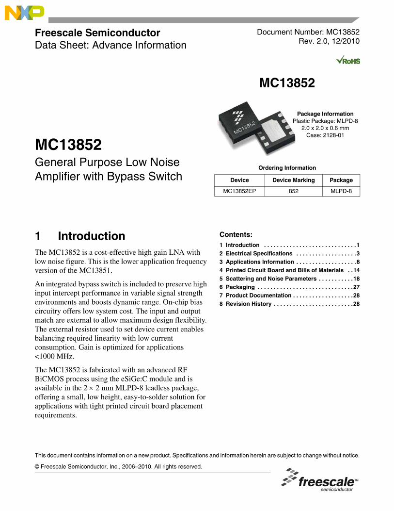
MC13852
Package InformationPlastic Package: MLPD-8
2.0 x 2.0 x 0.6 mmCase: 2128-01
Ordering Information
Device Device Marking Package
MC13852EP 852 MLPD-8
1 IntroductionThe MC13852 is a cost-effective high gain LNA with low noise figure. This is the lower application frequency version of the MC13851.
An integrated bypass switch is included to preserve high input intercept performance in variable signal strength environments and boosts dynamic range. On-chip bias circuitry offers low system cost. The input and output match are external to allow maximum design flexibility. The external resistor used to set device current enables balancing required linearity with low current consumption. Gain is optimized for applications <1000 MHz.
The MC13852 is fabricated with an advanced RF BiCMOS process using the eSiGe:C module and is available in the 2 × 2 mm MLPD-8 leadless package, offering a small, low height, easy-to-solder solution for applications with tight printed circuit board placement requirements.
MC13852General Purpose Low Noise Amplifier with Bypass Switch
Contents:1 Introduction . . . . . . . . . . . . . . . . . . . . . . . . . . . . .12 Electrical Specifications . . . . . . . . . . . . . . . . . . .33 Applications Information . . . . . . . . . . . . . . . . . . .84 Printed Circuit Board and Bills of Materials . .145 Scattering and Noise Parameters . . . . . . . . . . .186 Packaging . . . . . . . . . . . . . . . . . . . . . . . . . . . . . .277 Product Documentation . . . . . . . . . . . . . . . . . . .288 Revision History . . . . . . . . . . . . . . . . . . . . . . . . .28

Introduction
MC13852 Advance Information, Rev. 2.0
2 Freescale Semiconductor
1.1 Features• The MC13852 is intended for applications from 400 to 1000 MHz; the MC13851 is for
applications >1000 MHz.
• Gain: 20.3 dB (typ) at 434 MHz, 18.7 dB (typ) at 900 MHz.
• Output third order intercept point (OIP3): 10.6 dBm at 434 MHz, 14.2 dBm (typ) dBm at 900 MHz.
• Noise Figure (NF): 1.65 dB (typ) at 434 MHz, 1.2 dB at 900 MHz.
• Output 1 dB compression point (P1dB): 7.8 dBm (typ) at 434 MHz, 9.6 dBm (typ) at 900 MHz.
• IP3 Boost Circuitry.
• Bypass mode return losses are comparable to active mode, for use in systems with filters and duplexers.
• Bypass mode improves dynamic range in variable signal strength environments.
• Integrated logic-controlled standby mode with current drain < 1uA.
• Total supply current variable from 3–6 mA using an external bias resistor.
• Average current drain <0.6mA in a receiver lineup with 20% active / 80% bypass mode operation.
• On-chip bias sets the bias point.
• Bias stabilized for device and temperature variations.
• MLPD-8 leadless package with low parasitics.
• 434 MHz and 900 MHz application circuit evaluation boards with characterization data are available.
• Available in tape and reel packaging.
1.2 ApplicationsIdeal for use in any RF product that operates between 400 MHz and 1 GHz, and may be applied in:
• Buffer amplifiers
• Mixers
• IF amplifiers
• Voltage-controlled oscillators (VCOs)
• Use with transceivers requiring external LNAs
• RF smart metering
• Mobile: Cellular front-end LNA, 2-way radios
• Auto: RKE, key fob, TPMS
• Low current drain/long standby time for extended battery life applications
Figure 1 shows a simplified block diagram, with the pinouts and the location of the pin 1 marking on the package.

Electrical Specifications
MC13852 Advance Information, Rev. 2.0
Freescale Semiconductor 3
Figure 1. Simplified Block Diagram
2 Electrical SpecificationsTable 1 lists the maximum ratings for the device.
Table 2 lists the recommended operating conditions.
Table 1. Maximum Ratings
Ratings Symbol Value Unit
Supply Voltage VCC 3.3 V
Storage Temperature Range Tstg -65 to 150 °C
Operating Ambient Temperature Range TA -30 to 85 °C
RF Input Power Prf 10 dBm
Power Dissipation Pdis 100 mW
Thermal Resistance, Junction to Case RθJC 24 C/W
Thermal Resistance, Junction to Ambient, 4 Layer Board RθJA 90 C/W
NOTES: 1. Maximum Ratings are those values beyond which damage to the device may occur.Functional operation should be restricted to the limits in the Recommended OperatingConditions and Electrical Characteristics tables.
2. ESD (electrostatic discharge) immunity meets Human Body Model (HBM) ≤200 V, Charge Device Model (CDM) ≤450 V, and Machine Model (MM) ≤50 V. Additional ESD data available upon request.
Table 2. Recommended Operating Conditions
Characteristic Symbol Min Typ Max Unit
RF Frequency range fRF 400 — 1000 MHz
Supply Voltage VCC 2.3 2.75 3.0 Vdc
Logic VoltageInput High Voltage Input Low Voltage
— 1.25 0
1.8 —
VCC0.8
Vdc
RF OUT
2
5
7
6 GainLogic
Vcc
RF IN
3
1
Band
8
4 Enable
Rbias
Emit

Electrical Specifications
MC13852 Advance Information, Rev. 2.0
4 Freescale Semiconductor
Table 3 shows the use of the Gain, Enable and Band pins (along with the Vcc and RF out pins), to select Active mode (High Gain), Bypass mode (Low Gain), or Standby mode (Disable) operation.
Table 4 lists electrical characteristics associated with noise performance measured in a 50Ω system. Additional noise parameters are listed in Table 14 and Table 15. Also listed are the typical Icc and RF turn-on times for the device.
Table 5 lists the electrical characteristics measured on evaluation boards that are tuned for typical application frequencies. Further details on the application circuits are shown in Section 4; details on the boards are shown in Section 5.
Table 3. Truth Table
Pin Function Pin NameEnable Disable
Low Gain High Gain Low Gain High Gain
Logic Circuit Bias Vcc Vcc 1 1 1 1
Toggles Gain Mode (Active or Bypass) Gain 0 1 0 1
Toggles LNA On/Off Enable 1 1 0 0
Selects the LNA Band 1 1 1 1
NOTES: 1. Logic state "1" equals Vcc voltage. Logic state of "0" equals ground potential.2. Vcc is inductively coupled to LNA Out pin and Vcc pin.3. Minimum logic state "1" for enable and gain pins is 1.25V.4. Maximum logic state "0" for enable and gain pins is 0.8V.
Table 4. Electrical Characteristics (Vcc = 2.75 V, Ta = 25°C)
Characteristic Symbol Min Typ Max Unit
Insertion GainR1=1.2 kΩ, Freq=434 MHzR1=1.2 kΩ, Freq=900 MHz
|S21|2 20.416.4
21.918.3
— dB
Maximum Stable Gain and/or Maximum Available Gain [Note1]R1=1.2 kΩ, Freq=434 MHzR1=1.2 kΩ, Freq=900 MHz
MSG, MAG 26.722
28.223.5
— dB
Minimum Noise FigureR1=1.2 kΩ, Freq=434 MHzR1=1.2 kΩ, Freq=900 MHz
NFmin — 0.920.84
1.21.1
dB
Associated Gain at Minimum Noise FigureR1=1.2 kΩ, Freq=434 MHzR1=1.2 kΩ, Freq=900 MHz
Gnf 27.621
29.623
— dB
Icc and RF Turn On TimeEnable trigger total time of 1.8 usec from 0 to 2.75 V
Icc rise time from 0 to 76% of final current levelIcc rise time from 0 to 87% of final current levelRF on time from leading edge of enable trigger to RF turn-on
— — 6.49.61.37
— usec
NOTES: 1. Maximum Available Gain and Maximum Stable Gain are defined by the K factor as follows:MAG=|S21/S12(K+/-sqrt(K2-1))|, if K>1, MSG =|S21/S12|, if K<1
Electrical Specifications
MC13852 Advance Information, Rev. 2.0
Freescale Semiconductor 5
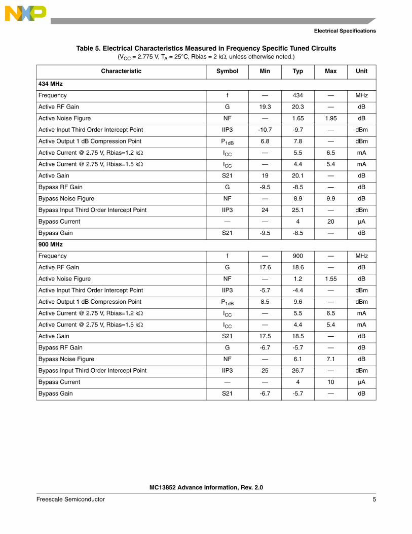
Table 5. Electrical Characteristics Measured in Frequency Specific Tuned Circuits(VCC = 2.775 V, TA = 25°C, Rbias = 2 kΩ, unless otherwise noted.)
Characteristic Symbol Min Typ Max Unit
434 MHz
Frequency f — 434 — MHz
Active RF Gain G 19.3 20.3 — dB
Active Noise Figure NF — 1.65 1.95 dB
Active Input Third Order Intercept Point IIP3 -10.7 -9.7 — dBm
Active Output 1 dB Compression Point P1dB 6.8 7.8 — dBm
Active Current @ 2.75 V, Rbias=1.2 kΩ ICC — 5.5 6.5 mA
Active Current @ 2.75 V, Rbias=1.5 kΩ ICC — 4.4 5.4 mA
Active Gain S21 19 20.1 — dB
Bypass RF Gain G -9.5 -8.5 — dB
Bypass Noise Figure NF — 8.9 9.9 dB
Bypass Input Third Order Intercept Point IIP3 24 25.1 — dBm
Bypass Current — — 4 20 µA
Bypass Gain S21 -9.5 -8.5 — dB
900 MHz
Frequency f — 900 — MHz
Active RF Gain G 17.6 18.6 — dB
Active Noise Figure NF — 1.2 1.55 dB
Active Input Third Order Intercept Point IIP3 -5.7 -4.4 — dBm
Active Output 1 dB Compression Point P1dB 8.5 9.6 — dBm
Active Current @ 2.75 V, Rbias=1.2 kΩ ICC — 5.5 6.5 mA
Active Current @ 2.75 V, Rbias=1.5 kΩ ICC — 4.4 5.4 mA
Active Gain S21 17.5 18.5 — dB
Bypass RF Gain G -6.7 -5.7 — dB
Bypass Noise Figure NF — 6.1 7.1 dB
Bypass Input Third Order Intercept Point IIP3 25 26.7 — dBm
Bypass Current — — 4 10 µA
Bypass Gain S21 -6.7 -5.7 — dB

Electrical Specifications
MC13852 Advance Information, Rev. 2.0
6 Freescale Semiconductor
Figure 2 and Figure 3 show maximum stable and maximum available gain and forward insertion gain versus frequency for the packaged device in a 50Ω system using bias resistors of 1.5 kΩ and 1.2 kΩ.
Figure 2. Maximum Stable/Available Gain and Forward Insertion Gain vs. Frequency, Rbias = 1.5 kΩ
Figure 3. Maximum Stable/Available Gain and Forward Insertion Gain vs. Frequency, Rbias = 1.2 kΩ
12
14
16
18
20
22
24
26
28
30
32
300 400 500 600 700 800 900 1000 1100 1200
Frequency (GHz)
MSG/MAG (dB)
|s21|^2 (dB)
|S21|2
MSG
MS
G, M
AG
, [S
21]2
(dB
)
[S21]2
12
14
16
18
20
22
24
26
28
30
32
300 400 500 600 700 800 900 1000 1100 1200
MSG/MAG (dB)
|s21|^2 (dB)
|S21|2
MSG
[S21]2
MS
G, M
AG
, [S
21]2 (
dB
)
Electrical Specifications
MC13852 Advance Information, Rev. 2.0
Freescale Semiconductor 7
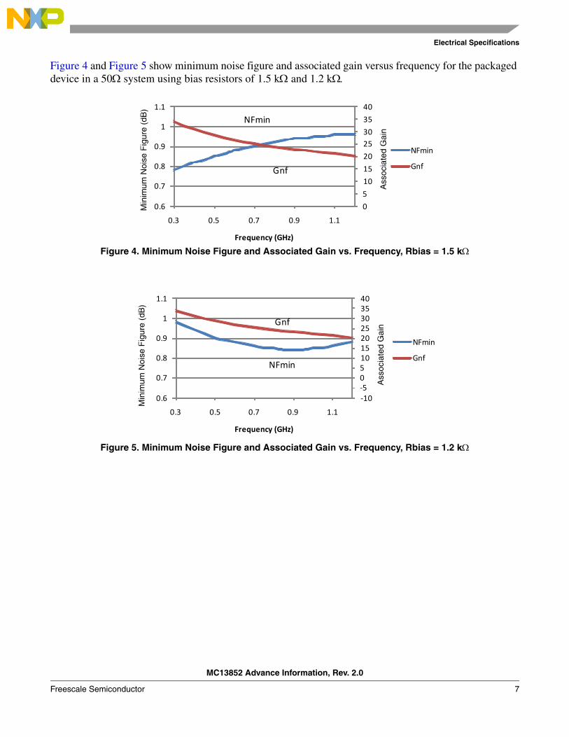
Figure 4 and Figure 5 show minimum noise figure and associated gain versus frequency for the packaged device in a 50Ω system using bias resistors of 1.5 kΩ and 1.2 kΩ.
Figure 4. Minimum Noise Figure and Associated Gain vs. Frequency, Rbias = 1.5 kΩ
Figure 5. Minimum Noise Figure and Associated Gain vs. Frequency, Rbias = 1.2 kΩ
0
5
10
15
20
2530
35
40
0.6
0.7
0.8
0.9
1
1.1
0.3 0.5 0.7 0.9 1.1
Frequency (GHz)
NFmin
GnfGnf
NFmin
Min
imum
Noi
se F
igur
e (d
B)
Ass
ocia
ted
Gai
n
‐10‐50510152025303540
0.6
0.7
0.8
0.9
1
1.1
0.3 0.5 0.7 0.9 1.1
Frequency (GHz)
NFmin
Gnf
Gnf
NFmin
Min
imum
Noi
se F
igur
e (d
B)
Ass
ocia
ted
Gai
n

Applications Information
MC13852 Advance Information, Rev. 2.0
8 Freescale Semiconductor
Figure 6 shows the Icc current drain for a range of values for the external bias resistor Rbias.
Figure 6. Icc vs. Bias Resistor R1 Value
3 Applications InformationThe MC13852 LNA is designed for applications in the 400 MHz to 1 GHz range. It has three different modes: High Gain, Low Gain (bypass) and Standby. The LNA is programmable through the Gain and Enable pins. The logic truth table is given in Table 3. The internal bypass switch is designed for broadband applications.
One of the advantages of the MC13852 is the simplification of the matching network in both bypass and amplifier modes. The bypass switch is designed so that changes of input and output return losses between bypass mode and active mode are minimized and the matching network design is simplified.
In these application examples, a balance is made between the competing RF performance characteristics of Icc, NF, gain, IP3, and return losses with unconditional stability. Conjugate matching is not used for the input or output. Instead, matching which achieves a trade-off in RF performance qualities is used. For a particular application or specification requirement, the matching can be changed to achieve enhanced performance of one parameter.
Measurements are made at a bias of Vcc = 2.75 V. Frequency spacing for IP3 measurements is 200 kHz. Non-linear measurements are made at Pin = -30 dBm. Typical application circuits are provided for 434 MHz and 900 MHz applications. Typical RF performance is shown for two values of bias resistor R1: 1.2 kΩ and 1.5 kΩ. These two current drain levels offer variations in intercept point, gain and noise figure. Included with each application are the schematics and electrical performance.
• Section 4 provides the evaluation board layout and Bill of Material for the circuits.
• Section 5 provides Smith charts with gain and noise circles for each application frequency.
y = 1.7619x2 ‐ 8.5883x + 13.293R² = 0.9983
2
2.5
3
3.5
4
4.5
5
5.5
6
6.5
1.1 1.3 1.5 1.7 1.9 2.1
Rbias value (kohm)
Icc mA
Poly. (Icc mA)
Icc
(mA
)

Applications Information
MC13852 Advance Information, Rev. 2.0
Freescale Semiconductor 9
3.1 434 MHz ApplicationThis application was designed to provide typical NF = 1.65 dB, S21 gain = 20 dB, OIP3 =10.6 dBm at 434 MHz. Typical performance that can be expected from this circuit at 2.75 V is listed in Table 6. The component values can be changed to enhance the performance of a particular parameter, but usually at the expense of another. Two values of bias resistor R1 are shown to demonstrate performance for different IP3 and Icc requirements.
• Values of external resistor R1 are varied to adjust Icc and IP3.
• Inductor L3 provides bias to the logic circuit.
Figure 7 is the 434 MHz application schematic with package pinouts and the circuit component topology.
Figure 7. 434 MHz Application Schematic
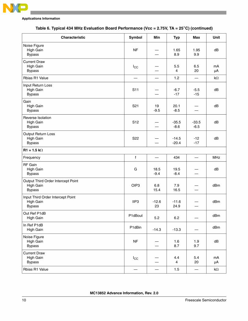
Table 6. Typical 434 MHz Evaluation Board Performance (Vcc = 2.75V, TA = 25°C)
Characteristic Symbol Min Typ Max Unit
R1 = 1.2 kΩ
Frequency f — 434 — MHz
RF GainHigh GainBypass
G 19.3-9.5
20.3-8.5
——
dB
Output Third Order Intercept PointHigh GainBypass
OIP3 9.515.5
10.616.6
——
dBm
Input Third Order Intercept PointHigh GainBypass
IIP3 -10.724
-9.725.1
——
dBm
Out Ref P1dBHigh Gain
P1dBout6.8 7.8 —
dBm
In Ref P1dBHigh Gain
P1dBin-13.5 -12.5 —
dBm
RF OUT
R230 ohm
L1 27 nH C2
47 pF
L2 47 nH
C533 pF
C40.1 uF
Gain
Vcc
.
Enable
RbiasR1 1.2 kohm
C3 22 pFG
ain
Enable
6
1
3
2
Logic
7
5 4
8 Emit
C1 1 .3 pF
R382 ohm
L3 270 nH
Applications Information
MC13852 Advance Information, Rev. 2.0
10 Freescale Semiconductor
Noise FigureHigh GainBypass
NF ——
1.658.9
1.959.9
dB
Current DrawHigh GainBypass
ICC ——
5.54
6.520
mAµA
Rbias R1 Value — — 1.2 — kΩ
Input Return LossHigh GainBypass
S11 ——
-6.7-17
-5.5-15
dB
GainHigh GainBypass
S21 19-9.5
20.1-8.5
——
dB
Reverse IsolationHigh GainBypass
S12 ——
-35.5-8.6
-33.5-6.5
dB
Output Return LossHigh GainBypass
S22 ——
-14.5-20.4
-12-17
dB
R1 = 1.5 kΩ
Frequency f — 434 — MHz
RF GainHigh GainBypass
G 18.5-9.4
19.5-8.4
——
dB
Output Third Order Intercept PointHigh GainBypass
OIP3 6.815.4
7.916.5
——
dBm
Input Third Order Intercept PointHigh GainBypass
IIP3 -12.623
-11.624.9
——
dBm
Out Ref P1dBHigh Gain
P1dBout5.2 6.2 —
dBm
In Ref P1dBHigh Gain
P1dBin-14.3 -13.3 —
dBm
Noise FigureHigh GainBypass
NF ——
1.68.7
1.99.7
dB
Current DrawHigh GainBypass
ICC ——
4.44
5.420
mAµA
Rbias R1 Value — — 1.5 — kΩ
Table 6. Typical 434 MHz Evaluation Board Performance (Vcc = 2.75V, TA = 25°C) (continued)
Characteristic Symbol Min Typ Max Unit
Applications Information
MC13852 Advance Information, Rev. 2.0
Freescale Semiconductor 11
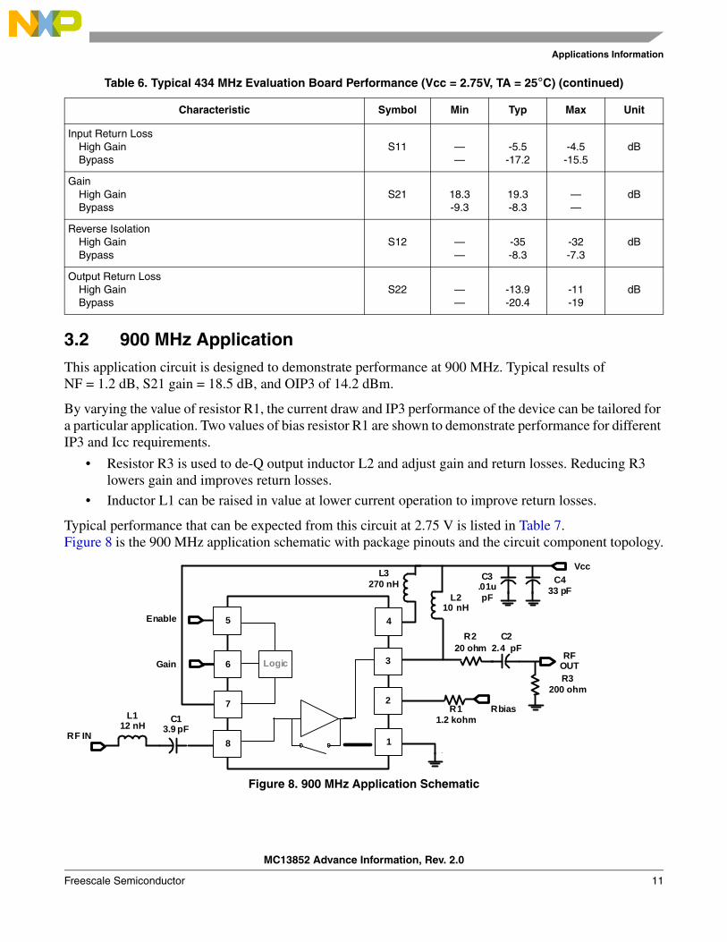
3.2 900 MHz ApplicationThis application circuit is designed to demonstrate performance at 900 MHz. Typical results of NF = 1.2 dB, S21 gain = 18.5 dB, and OIP3 of 14.2 dBm.
By varying the value of resistor R1, the current draw and IP3 performance of the device can be tailored for a particular application. Two values of bias resistor R1 are shown to demonstrate performance for different IP3 and Icc requirements.
• Resistor R3 is used to de-Q output inductor L2 and adjust gain and return losses. Reducing R3 lowers gain and improves return losses.
• Inductor L1 can be raised in value at lower current operation to improve return losses.
Typical performance that can be expected from this circuit at 2.75 V is listed in Table 7.Figure 8 is the 900 MHz application schematic with package pinouts and the circuit component topology.
Figure 8. 900 MHz Application Schematic
Input Return LossHigh GainBypass
S11 ——
-5.5-17.2
-4.5-15.5
dB
GainHigh GainBypass
S21 18.3-9.3
19.3-8.3
——
dB
Reverse IsolationHigh GainBypass
S12 ——
-35-8.3
-32-7.3
dB
Output Return LossHigh GainBypass
S22 ——
-13.9-20.4
-11-19
dB
Table 6. Typical 434 MHz Evaluation Board Performance (Vcc = 2.75V, TA = 25°C) (continued)
Characteristic Symbol Min Typ Max Unit
RF OUT
R220 ohm
L1 12 nH
C1 3.9 pF
L2 10 nH
C433 pF
C3.01u pF
Gain
Vcc
RF IN.
Enable
RbiasR1 1.2 kohm
C2 2.4 pFG
ain
Enable
6
1
3
2
Logic
7
5 4
8
R3200 ohm
L3 270 nH
Applications Information
MC13852 Advance Information, Rev. 2.0
12 Freescale Semiconductor
Table 7. Typical 900 MHz Evaluation Board Performance (Vcc = 2.75V, TA = 25°C)
Characteristic Symbol Min Typ Max Unit
R1 = 1.2 kΩ
Frequency f — 900 — MHz
RF GainHigh GainBypass
G 17.6-6.7
18.6-5.7
——
dB
Output Third Order Intercept PointHigh GainBypass
OIP3 1319.5
14.221
——
dBm
Input Third Order Intercept PointHigh GainBypass
IIP3 -5.425
-4.426.7
——
dBm
Out Ref P1dBHigh Gain
P1dBout8.5 9.6 —
dBm
In Ref P1dBHigh Gain
P1dBin-9.9 -8.9 —
dBm
Noise FigureHigh GainBypass
NF ——
1.26.1
1.557.1
dB
Current DrawHigh GainBypass
ICC ——
5.54
6.520
mAµA
Rbias R1 Value — — 1.2 — kΩ
Input Return LossHigh GainBypass
S11 ——
-8.8-11
-7-9
dB
GainHigh GainBypass
S21 17.5-6.7
18.5-5.7
——
dB
Reverse IsolationHigh GainBypass
S12 ——
-28-5.7
-26.5-4.7
dB
Output Return LossHigh GainBypass
S22 ——
-13-25
-10-20
dB
R1 = 1.5 kΩ
Frequency f — 900 — MHz
RF GainHigh GainBypass
G 17.2-7.7
18.2-5.7
——
dB
Output Third Order Intercept PointHigh GainBypass
OIP3 12.119.8
13.121
——
dBm

Applications Information
MC13852 Advance Information, Rev. 2.0
Freescale Semiconductor 13
Input Third Order Intercept PointHigh GainBypass
IIP3 -6.225.5
-5.126.7
——
dBm
Out Ref P1dBHigh Gain
P1dBout8.5 9.9 —
dBm
In Ref P1dBHigh Gain
P1dBin-10 -8.4 —
dBm
Noise FigureHigh GainBypass
NF ——
1.186.1
1.57.1
dB
Current DrawHigh GainBypass
ICC ——
4.44
5.420
mAµA
Rbias R1 Value — — 1.5 — kΩ
Input Return LossHigh GainBypass
S11 ——
-7.6-11
-6.2-9
dB
GainHigh GainBypass
S21 17.2-6.7
18.2-5.7
——
dB
Reverse IsolationHigh GainBypass
S12 ——
-27.7-5.7
-26.7-4.7
dB
Output Return LossHigh GainBypass
S22 ——
-12.5-25
-10-20
dB
Table 7. Typical 900 MHz Evaluation Board Performance (Vcc = 2.75V, TA = 25°C) (continued)
Characteristic Symbol Min Typ Max Unit
Printed Circuit Board and Bills of Materials
MC13852 Advance Information, Rev. 2.0
14 Freescale Semiconductor
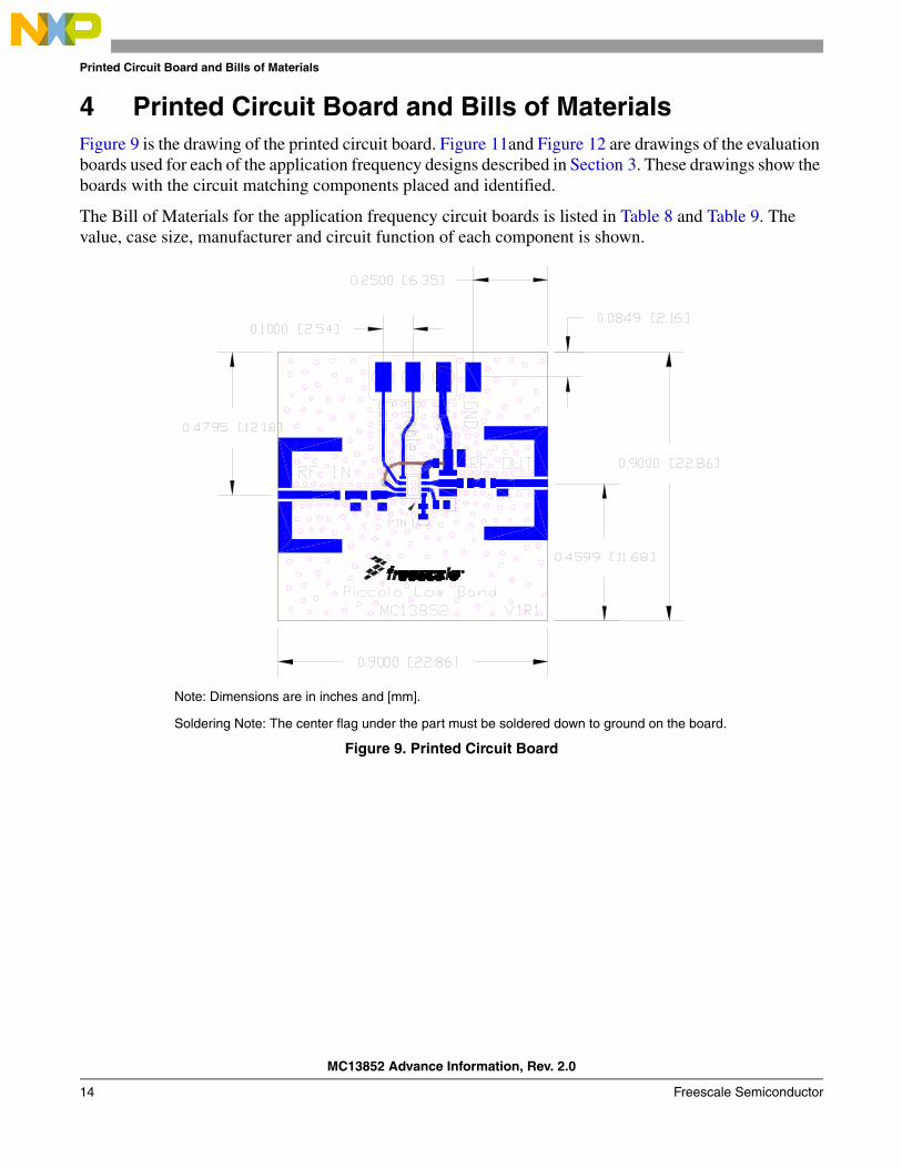
4 Printed Circuit Board and Bills of MaterialsFigure 9 is the drawing of the printed circuit board. Figure 11and Figure 12 are drawings of the evaluation boards used for each of the application frequency designs described in Section 3. These drawings show the boards with the circuit matching components placed and identified.
The Bill of Materials for the application frequency circuit boards is listed in Table 8 and Table 9. The value, case size, manufacturer and circuit function of each component is shown.
Figure 9. Printed Circuit Board
Note: Dimensions are in inches and [mm].
Soldering Note: The center flag under the part must be soldered down to ground on the board.
Printed Circuit Board and Bills of Materials
MC13852 Advance Information, Rev. 2.0
Freescale Semiconductor 15
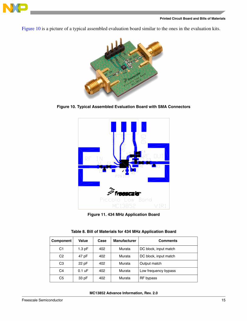
Figure 10 is a picture of a typical assembled evaluation board similar to the ones in the evaluation kits.
Figure 10. Typical Assembled Evaluation Board with SMA Connectors
Figure 11. 434 MHz Application Board
Table 8. Bill of Materials for 434 MHz Application Board
Component Value Case Manufacturer Comments
C1 1.3 pF 402 Murata DC block, input match
C2 47 pF 402 Murata DC block, input match
C3 22 pF 402 Murata Output match
C4 0.1 uF 402 Murata Low frequency bypass
C5 33 pF 402 Murata RF bypass

Printed Circuit Board and Bills of Materials
MC13852 Advance Information, Rev. 2.0
16 Freescale Semiconductor
Figure 12. 900 MHz Application Board
L1 27 nH 402 Murata Input match
L2 47 nH 402 Murata Output match, bias decouple
L3 270 nH 402 Murata Bias couple to logic
R1 1.2 kΩ 402 KOA Bias set point
R2 30 Ω 402 KOA Stability, lower gain
R3 82 Ω 402 KOA L2 de-Q, gain adjust
Q1 MC13852 MLP 2x2 Freescale SiGe LNA
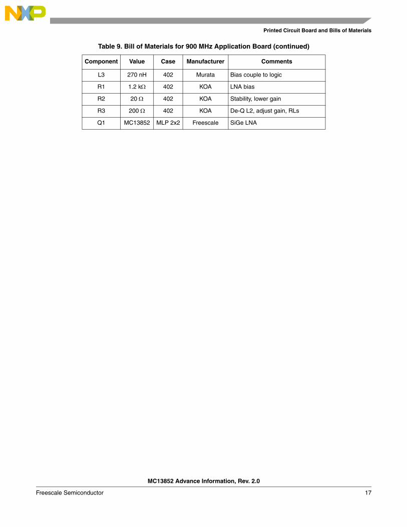
Table 9. Bill of Materials for 900 MHz Application Board
Component Value Case Manufacturer Comments
C1 3.9 pF 402 Murata Input match
C2 2.4 pF 402 Murata Output match
C3 0.1 uF 402 Murata Low frequency bypass
C4 33 pF 402 Murata RF bypass
L1 12 nH 402 Murata Input match
L2 10 nH 402 Murata Output match
Table 8. Bill of Materials for 434 MHz Application Board (continued)
Component Value Case Manufacturer Comments
Printed Circuit Board and Bills of Materials
MC13852 Advance Information, Rev. 2.0
Freescale Semiconductor 17
L3 270 nH 402 Murata Bias couple to logic
R1 1.2 kΩ 402 KOA LNA bias
R2 20 Ω 402 KOA Stability, lower gain
R3 200 Ω 402 KOA De-Q L2, adjust gain, RLs
Q1 MC13852 MLP 2x2 Freescale SiGe LNA
Table 9. Bill of Materials for 900 MHz Application Board (continued)
Component Value Case Manufacturer Comments
Scattering and Noise Parameters
MC13852 Advance Information, Rev. 2.0
18 Freescale Semiconductor
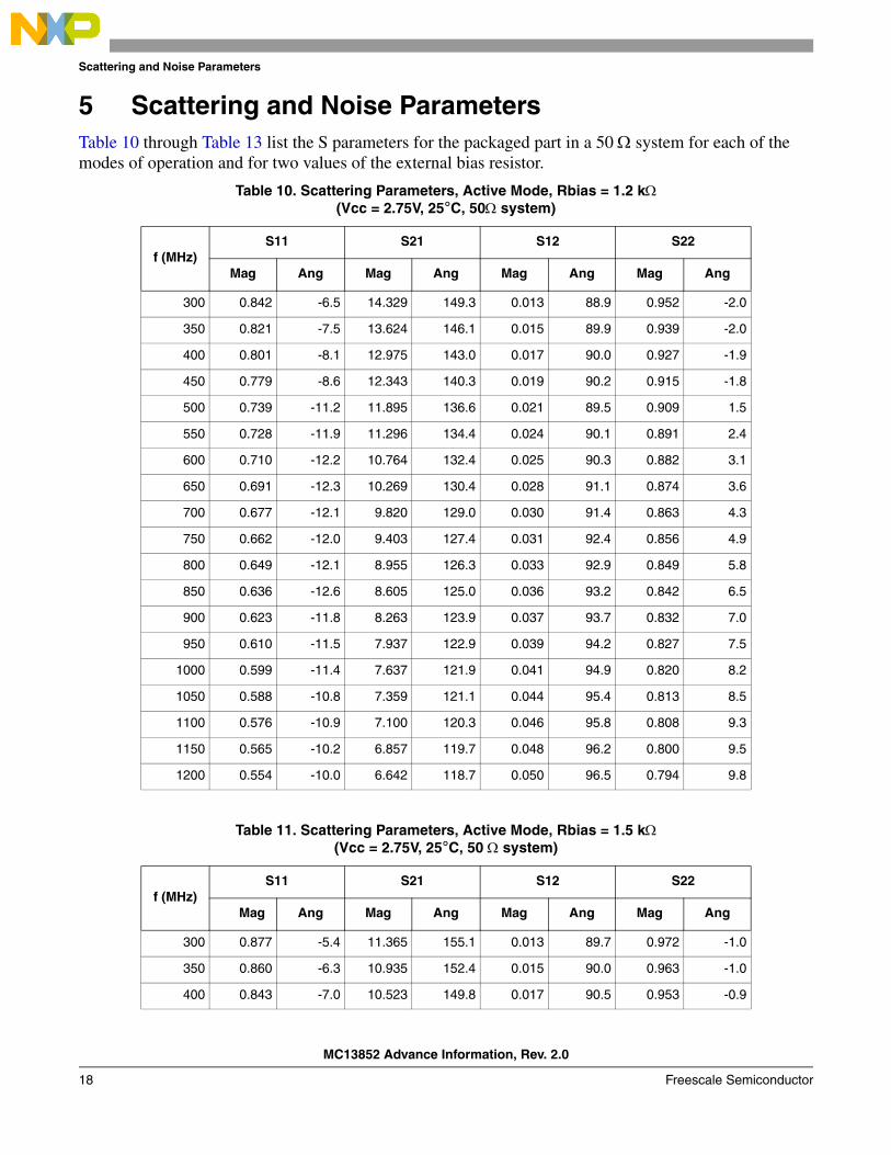
5 Scattering and Noise ParametersTable 10 through Table 13 list the S parameters for the packaged part in a 50 Ω system for each of the modes of operation and for two values of the external bias resistor.
Table 10. Scattering Parameters, Active Mode, Rbias = 1.2 kΩ(Vcc = 2.75V, 25°C, 50Ω system)
f (MHz)S11 S21 S12 S22
Mag Ang Mag Ang Mag Ang Mag Ang
300 0.842 -6.5 14.329 149.3 0.013 88.9 0.952 -2.0
350 0.821 -7.5 13.624 146.1 0.015 89.9 0.939 -2.0
400 0.801 -8.1 12.975 143.0 0.017 90.0 0.927 -1.9
450 0.779 -8.6 12.343 140.3 0.019 90.2 0.915 -1.8
500 0.739 -11.2 11.895 136.6 0.021 89.5 0.909 1.5
550 0.728 -11.9 11.296 134.4 0.024 90.1 0.891 2.4
600 0.710 -12.2 10.764 132.4 0.025 90.3 0.882 3.1
650 0.691 -12.3 10.269 130.4 0.028 91.1 0.874 3.6
700 0.677 -12.1 9.820 129.0 0.030 91.4 0.863 4.3
750 0.662 -12.0 9.403 127.4 0.031 92.4 0.856 4.9
800 0.649 -12.1 8.955 126.3 0.033 92.9 0.849 5.8
850 0.636 -12.6 8.605 125.0 0.036 93.2 0.842 6.5
900 0.623 -11.8 8.263 123.9 0.037 93.7 0.832 7.0
950 0.610 -11.5 7.937 122.9 0.039 94.2 0.827 7.5
1000 0.599 -11.4 7.637 121.9 0.041 94.9 0.820 8.2
1050 0.588 -10.8 7.359 121.1 0.044 95.4 0.813 8.5
1100 0.576 -10.9 7.100 120.3 0.046 95.8 0.808 9.3
1150 0.565 -10.2 6.857 119.7 0.048 96.2 0.800 9.5
1200 0.554 -10.0 6.642 118.7 0.050 96.5 0.794 9.8
Table 11. Scattering Parameters, Active Mode, Rbias = 1.5 kΩ(Vcc = 2.75V, 25°C, 50 Ω system)
f (MHz)S11 S21 S12 S22
Mag Ang Mag Ang Mag Ang Mag Ang
300 0.877 -5.4 11.365 155.1 0.013 89.7 0.972 -1.0
350 0.860 -6.3 10.935 152.4 0.015 90.0 0.963 -1.0
400 0.843 -7.0 10.523 149.8 0.017 90.5 0.953 -0.9
Scattering and Noise Parameters
MC13852 Advance Information, Rev. 2.0
Freescale Semiconductor 19
450 0.825 -7.6 10.136 147.5 0.020 90.8 0.944 -0.9
500 0.788 -10.4 9.908 144.0 0.022 89.8 0.943 2.2
550 0.777 -11.2 9.493 141.9 0.024 90.0 0.926 3.0
600 0.761 -11.8 9.128 139.9 0.026 90.5 0.918 3.6
650 0.743 -12.1 8.795 138.1 0.028 90.8 0.911 4.0
700 0.730 -12.1 8.513 136.7 0.030 91.2 0.901 4.4
750 0.713 -12.3 8.228 135.1 0.032 91.8 0.894 4.9
800 0.699 -12.6 7.875 134.0 0.034 92.1 0.887 5.8
850 0.686 -13.3 7.624 132.7 0.036 92.2 0.879 6.4
900 0.670 -12.7 7.375 131.5 0.038 92.9 0.870 6.8
950 0.655 -12.6 7.125 130.3 0.040 93.6 0.864 7.4
1000 0.642 -12.5 6.885 129.2 0.042 93.7 0.856 8.0
1050 0.630 -12.1 6.667 128.3 0.044 94.3 0.849 8.3
1100 0.616 -12.2 6.457 127.4 0.046 95.0 0.845 9.1
1150 0.603 -11.7 6.264 126.7 0.048 95.6 0.838 9.4
1200 0.592 -11.5 6.084 125.6 0.050 95.8 0.831 9.7
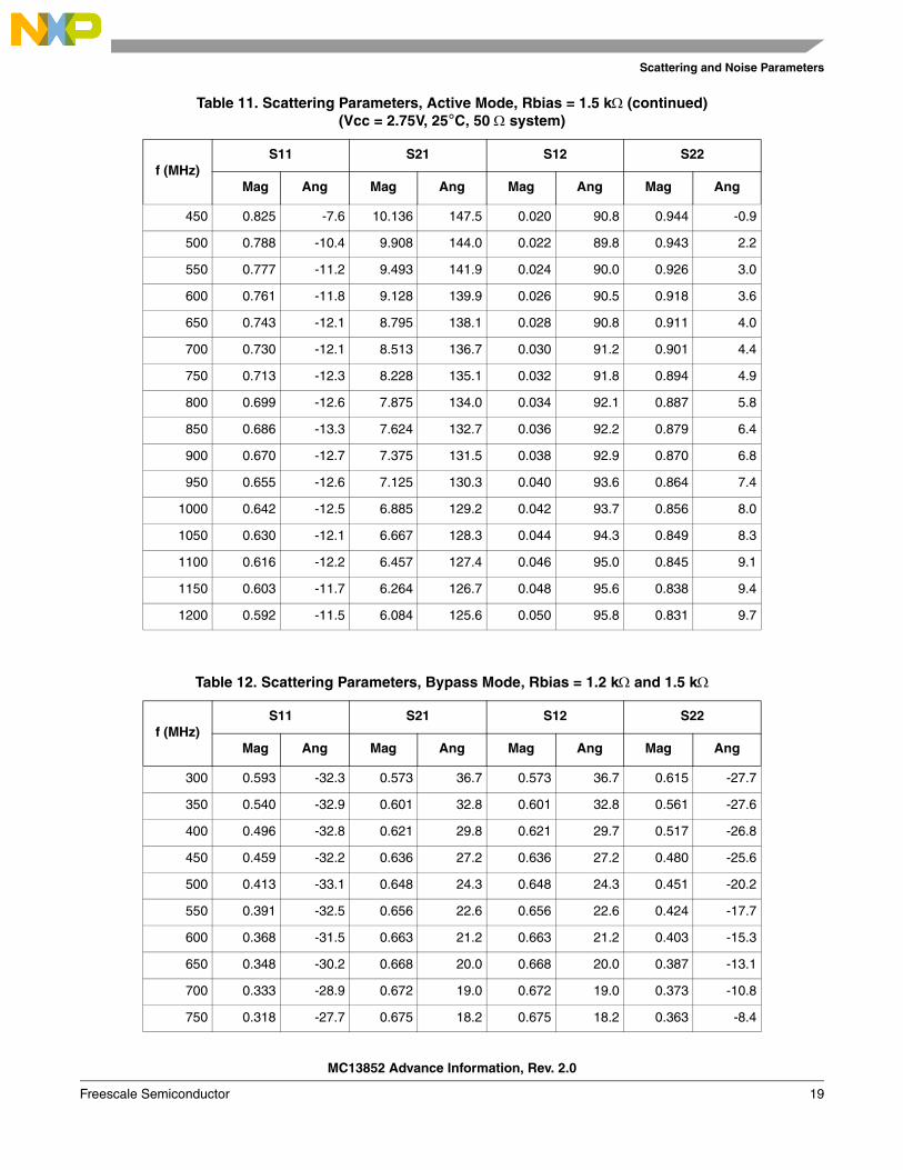
Table 12. Scattering Parameters, Bypass Mode, Rbias = 1.2 kΩ and 1.5 kΩ
f (MHz)S11 S21 S12 S22
Mag Ang Mag Ang Mag Ang Mag Ang
300 0.593 -32.3 0.573 36.7 0.573 36.7 0.615 -27.7
350 0.540 -32.9 0.601 32.8 0.601 32.8 0.561 -27.6
400 0.496 -32.8 0.621 29.8 0.621 29.7 0.517 -26.8
450 0.459 -32.2 0.636 27.2 0.636 27.2 0.480 -25.6
500 0.413 -33.1 0.648 24.3 0.648 24.3 0.451 -20.2
550 0.391 -32.5 0.656 22.6 0.656 22.6 0.424 -17.7
600 0.368 -31.5 0.663 21.2 0.663 21.2 0.403 -15.3
650 0.348 -30.2 0.668 20.0 0.668 20.0 0.387 -13.1
700 0.333 -28.9 0.672 19.0 0.672 19.0 0.373 -10.8
750 0.318 -27.7 0.675 18.2 0.675 18.2 0.363 -8.4
Table 11. Scattering Parameters, Active Mode, Rbias = 1.5 kΩ (continued)(Vcc = 2.75V, 25°C, 50 Ω system)
f (MHz)S11 S21 S12 S22
Mag Ang Mag Ang Mag Ang Mag Ang

Scattering and Noise Parameters
MC13852 Advance Information, Rev. 2.0
20 Freescale Semiconductor
800 0.305 -26.7 0.678 17.4 0.678 17.4 0.353 -5.9
850 0.292 -25.8 0.68 16.8 0.679 16.7 0.345 -3.4
900 0.282 -24.4 0.682 16.2 0.682 16.2 0.337 -1.3
950 0.272 -23.2 0.683 15.8 0.683 15.7 0.332 0.6
1000 0.263 -22.3 0.685 15.3 0.684 15.3 0.327 2.8
1050 0.256 -21.1 0.685 15.0 0.685 15.0 0.323 4.5
1100 0.247 -20.3 0.686 14.6 0.686 14.6 0.320 6.5
1150 0.239 -19.2 0.687 14.3 0.687 14.3 0.316 8.1
1200 0.231 -18.4 0.688 14.1 0.688 14.1 0.314 9.5
Table 13. Scattering Parameters, Standby Mode, Rbias = 1.2 kΩ and 1.5 kΩ(Vcc = 2.75V, 25°C, 50 Ω system)
f (MHz)S11 S21 S12 S22
Mag Ang Mag Ang Mag Ang Mag Ang
300 0.974 -0.3 0.013 95.0 0.014 94.8 0.996 3.5
350 0.973 -0.2 0.016 95.5 0.016 95.1 0.994 4.1
400 0.972 -0.2 0.018 96.2 0.018 95.5 0.993 4.7
450 0.971 -0.1 0.020 96.7 0.021 96.5 0.992 5.2
500 0.956 -2.7 0.023 95.1 0.023 95.1 1.007 8.5
550 0.960 -3.2 0.026 95.8 0.026 96.0 0.999 9.6
600 0.958 -3.6 0.028 96.2 0.028 95.9 1.000 10.4
650 0.953 -3.7 0.031 96.7 0.031 96.6 1.001 11.0
700 0.952 -3.9 0.033 97.1 0.033 97.0 0.997 11.7
750 0.949 -4.1 0.036 97.5 0.036 97.5 0.998 12.4
800 0.946 -4.6 0.039 97.7 0.039 97.7 0.998 13.2
850 0.940 -5.2 0.041 98.1 0.041 97.9 0.998 14.0
900 0.941 -5.1 0.044 98.3 0.044 98.2 0.994 14.5
950 0.937 -5.3 0.047 98.8 0.047 98.8 0.994 15.0
1000 0.934 -5.7 0.049 98.9 0.049 98.8 0.993 15.6
Table 12. Scattering Parameters, Bypass Mode, Rbias = 1.2 kΩ and 1.5 kΩ (continued)
f (MHz)S11 S21 S12 S22
Mag Ang Mag Ang Mag Ang Mag Ang
Scattering and Noise Parameters
MC13852 Advance Information, Rev. 2.0
Freescale Semiconductor 21
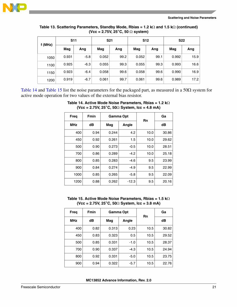
Table 14 and Table 15 list the noise parameters for the packaged part, as measured in a 50Ω system for active mode operation for two values of the external bias resistor.
1050 0.931 -5.8 0.052 99.2 0.052 99.1 0.992 15.9
1100 0.925 -6.3 0.055 99.3 0.055 99.3 0.993 16.6
1150 0.923 -6.4 0.058 99.6 0.058 99.6 0.990 16.9
1200 0.919 -6.7 0.061 99.7 0.061 99.6 0.989 17.2
Table 14. Active Mode Noise Parameters, Rbias = 1.2 kΩ(Vcc = 2.75V, 25°C, 50Ω System, Icc = 4.8 mA)
Freq Fmin Gamma OptRn
Ga
MHz dB Mag Angle dB
400 0.94 0.244 4.2 10.0 30.86
450 0.92 0.261 1.5 10.0 29.62
500 0.90 0.273 -0.5 10.0 28.51
700 0.86 0.289 -4.2 10.0 25.18
800 0.85 0.283 -4.6 9.5 23.99
900 0.84 0.274 -4.9 9.5 22.99
1000 0.85 0.265 -5.8 9.5 22.09
1200 0.88 0.262 -12.3 9.5 20.16
Table 15. Active Mode Noise Parameters, Rbias = 1.5 kΩ(Vcc = 2.75V, 25°C, 50Ω System, Icc = 3.8 mA)
Freq Fmin Gamma OptRn
Ga
MHz dB Mag Angle dB
400 0.82 0.313 0.23 10.5 30.82
450 0.83 0.323 0.5 10.5 29.52
500 0.85 0.331 -1.0 10.5 28.37
700 0.90 0.337 -4.3 10.5 24.94
800 0.92 0.331 -5.0 10.5 23.75
900 0.94 0.322 -5.7 10.5 22.76
Table 13. Scattering Parameters, Standby Mode, Rbias = 1.2 kΩ and 1.5 kΩ (continued)(Vcc = 2.75V, 25°C, 50 Ω system)
f (MHz)S11 S21 S12 S22
Mag Ang Mag Ang Mag Ang Mag Ang
Scattering and Noise Parameters
MC13852 Advance Information, Rev. 2.0
22 Freescale Semiconductor
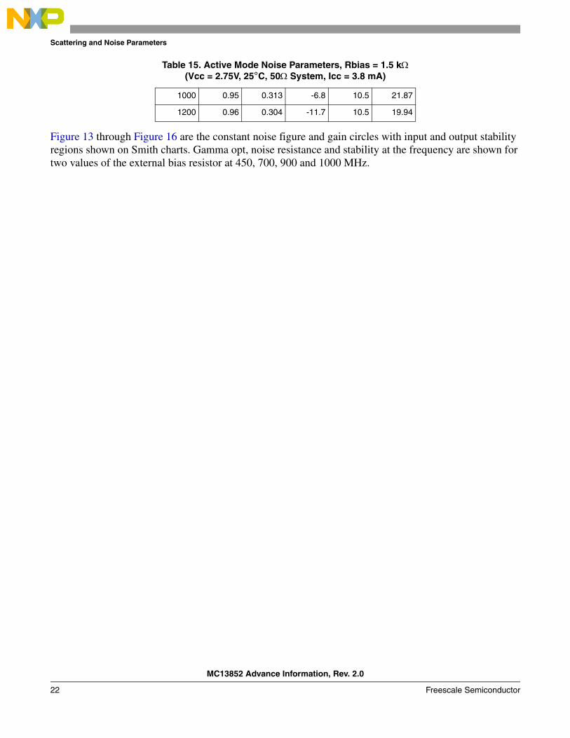
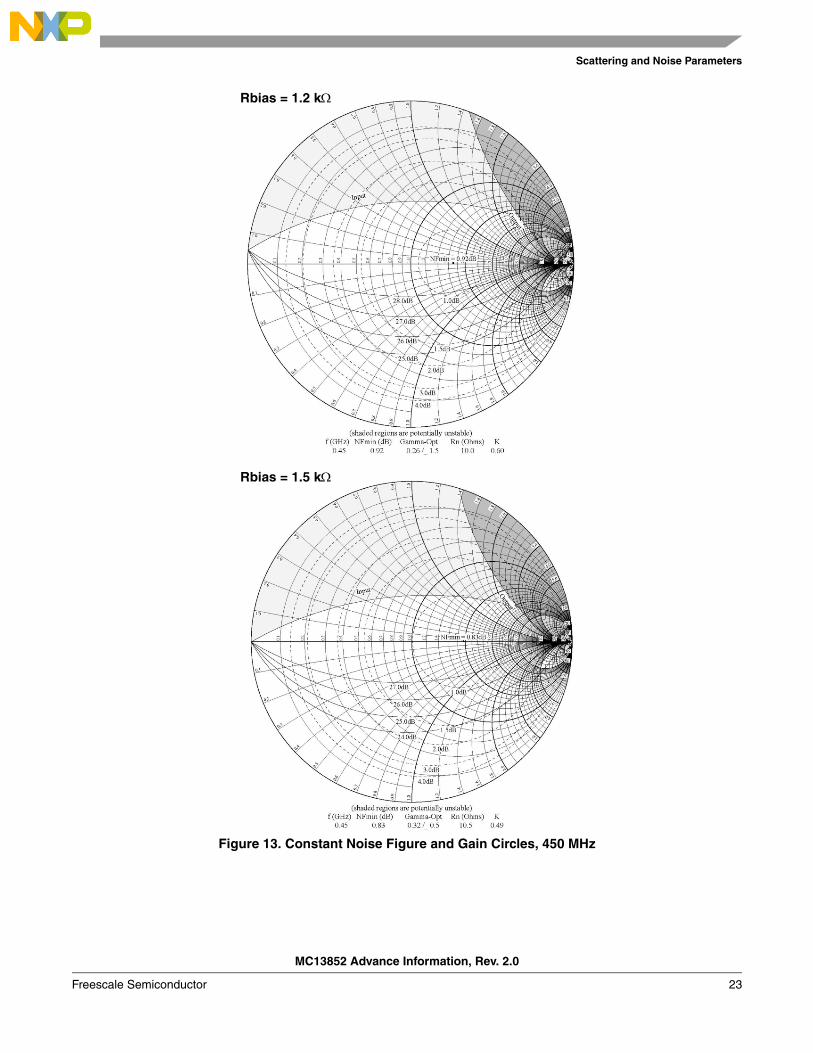
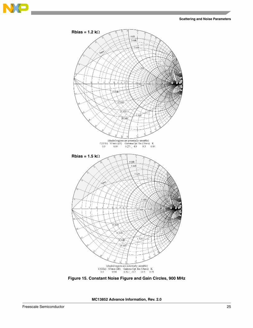
Figure 13 through Figure 16 are the constant noise figure and gain circles with input and output stability regions shown on Smith charts. Gamma opt, noise resistance and stability at the frequency are shown for two values of the external bias resistor at 450, 700, 900 and 1000 MHz.
1000 0.95 0.313 -6.8 10.5 21.87
1200 0.96 0.304 -11.7 10.5 19.94
Table 15. Active Mode Noise Parameters, Rbias = 1.5 kΩ(Vcc = 2.75V, 25°C, 50Ω System, Icc = 3.8 mA)
Scattering and Noise Parameters
MC13852 Advance Information, Rev. 2.0
Freescale Semiconductor 23
Figure 13. Constant Noise Figure and Gain Circles, 450 MHz
Rbias = 1.2 kΩ
Rbias = 1.5 kΩ

Scattering and Noise Parameters
MC13852 Advance Information, Rev. 2.0
24 Freescale Semiconductor
Figure 14. Constant Noise Figure and Gain Circles, 700 MHz
Rbias = 1.2 kΩ
Rbias = 1.5 kΩ
Scattering and Noise Parameters
MC13852 Advance Information, Rev. 2.0
Freescale Semiconductor 25
Figure 15. Constant Noise Figure and Gain Circles, 900 MHz
Rbias = 1.2 kΩ
Rbias = 1.5 kΩ
Scattering and Noise Parameters
MC13852 Advance Information, Rev. 2.0
26 Freescale Semiconductor
Figure 16. Constant Noise Figure and Gain Circles, 1000 MHz
Rbias = 1.2 kΩ
Rbias = 1.5 kΩ

Packaging
MC13852 Advance Information, Rev. 2.0
Freescale Semiconductor 27
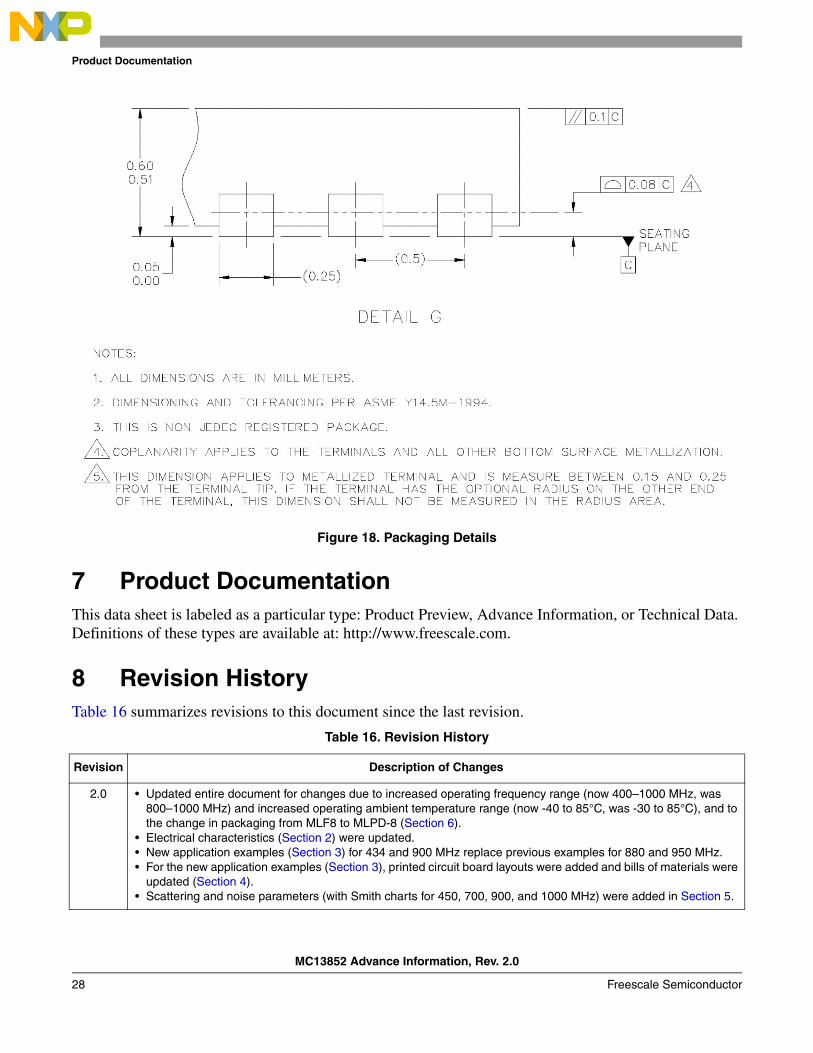
6 PackagingFigure 17 and Figure 18 are the package drawings with dimensions for the MLPD-8, 2 × 2 × 0.6 mm, package.
Figure 17. Outline Dimensions for MLPD-8
Product Documentation
MC13852 Advance Information, Rev. 2.0
28 Freescale Semiconductor
Figure 18. Packaging Details
7 Product DocumentationThis data sheet is labeled as a particular type: Product Preview, Advance Information, or Technical Data. Definitions of these types are available at: http://www.freescale.com.
8 Revision HistoryTable 16 summarizes revisions to this document since the last revision.
Table 16. Revision History
Revision Description of Changes
2.0 • Updated entire document for changes due to increased operating frequency range (now 400–1000 MHz, was 800–1000 MHz) and increased operating ambient temperature range (now -40 to 85°C, was -30 to 85°C), and to the change in packaging from MLF8 to MLPD-8 (Section 6).
• Electrical characteristics (Section 2) were updated. • New application examples (Section 3) for 434 and 900 MHz replace previous examples for 880 and 950 MHz. • For the new application examples (Section 3), printed circuit board layouts were added and bills of materials were
updated (Section 4). • Scattering and noise parameters (with Smith charts for 450, 700, 900, and 1000 MHz) were added in Section 5.

Revision History
MC13852 Advance Information, Rev. 2.0
Freescale Semiconductor 29
Document Number: MC13852Rev. 2.012/2010
How to Reach Us:
Home Page:www.freescale.com
Web Support:http://www.freescale.com/support
USA/Europe or Locations Not Listed:Freescale Semiconductor, Inc.Technical Information Center, EL5162100 East Elliot RoadTempe, Arizona 852841-800-521-6274 or +1-480-768-2130www.freescale.com/support
Europe, Middle East, and Africa:Freescale Halbleiter Deutschland GmbHTechnical Information CenterSchatzbogen 781829 Muenchen, Germany+44 1296 380 456 (English)+46 8 52200080 (English)+49 89 92103 559 (German)+33 1 69 35 48 48 (French)www.freescale.com/support
Japan:Freescale Semiconductor Japan Ltd.HeadquartersARCO Tower 15F1-8-1, Shimo-Meguro, Meguro-ku,Tokyo 153-0064Japan0120 191014 or +81 3 5437 [email protected]
Asia/Pacific:Freescale Semiconductor China Ltd.Exchange Building 23FNo. 118 Jianguo RoadChaoyang DistrictBeijing 100022 China +86 10 5879 [email protected]
For Literature Requests Only:Freescale Semiconductor Literature Distribution Center1-800-441-2447 or +1-303-675-2140Fax: [email protected]
Information in this document is provided solely to enable system and software implementers to use Freescale Semiconductor products. There are no express or implied copyright licenses granted hereunder to design or fabricate any integrated circuits or integrated circuits based on the information in this document.
Freescale Semiconductor reserves the right to make changes without further notice to any products herein. Freescale Semiconductor makes no warranty, representation or guarantee regarding the suitability of its products for any particular purpose, nor does Freescale Semiconductor assume any liability arising out of the application or use of any product or circuit, and specifically disclaims any and all liability, including without limitation consequential or incidental damages. “Typical” parameters that may be provided in Freescale Semiconductor data sheets and/or specifications can and do vary in different applications and actual performance may vary over time. All operating parameters, including “Typicals”, must be validated for each customer application by customer’s technical experts. Freescale Semiconductor does not convey any license under its patent rights nor the rights of others. Freescale Semiconductor products are not designed, intended, or authorized for use as components in systems intended for surgical implant into the body, or other applications intended to support or sustain life, or for any other application in which the failure of the Freescale Semiconductor product could create a situation where personal injury or death may occur. Should Buyer purchase or use Freescale Semiconductor products for any such unintended or unauthorized application, Buyer shall indemnify and hold Freescale Semiconductor and its officers, employees, subsidiaries, affiliates, and distributors harmless against all claims, costs, damages, and expenses, and reasonable attorney fees arising out of, directly or indirectly, any claim of personal injury or death associated with such unintended or unauthorized use, even if such claim alleges that Freescale Semiconductor was negligent regarding the design or manufacture of the part.
Freescale™ and the Freescale logo are trademarks of Freescale Semiconductor, Inc. All other product or service names are the property of their respective owners.
© Freescale Semiconductor, Inc. 2006-2010. All rights reserved.
RoHS-compliant and/or Pb-free versions of Freescale products have the functionality and electrical characteristics as their non-RoHS-compliant and/or non-Pb-free counterparts. For further information, see http://www.freescale.com or contact your Freescale sales representative.
For information on Freescale’s Environmental Products program, go to http://www.freescale.com/epp.