data image corporation tft module specification · data image corporation tft module specification...
TRANSCRIPT
Confidential Document
FG0700Q5DSSWBG01 REV: B Page: 1 /23
DATA IMAGE CORPORATION
TFT Module Specification
ITEM NO.: FG0700Q5DSSWBG01
Table of Contents
1. COVER & CONTENTS 1
2. RECORD OF REVISION 2
3. GENERAL SPECIFICATIONS 3
4. ABSOLUTE MAXIMUM RATINGS 3
5. ELECTRICAL CHARACTERISTICS 3
6. TIMING CHARACTERISTIC 5
7. OPTICAL CHARACTERISTIC 9
8. PIN CONNECTIONS 12
9. BLOCK DIAGRAM 14
10. QUALITY ASSURANCE 15
11. LCM PRODUCT LABEL DEFINE 19
12. PRECAUTIONS IN USE LCM 21
13. OUTLINE DRAWING 22
14. PACKAGE INFORMATION 23
Customer Companies QA Approval QA Check R&D Approval R&D Check
Approved by Version: Issued Date: Sheet Code: Total Pages:
B
24/NOV/16’ 23
Confidential Document
FG0700Q5DSSWBG01 REV: B Page: 2 /23
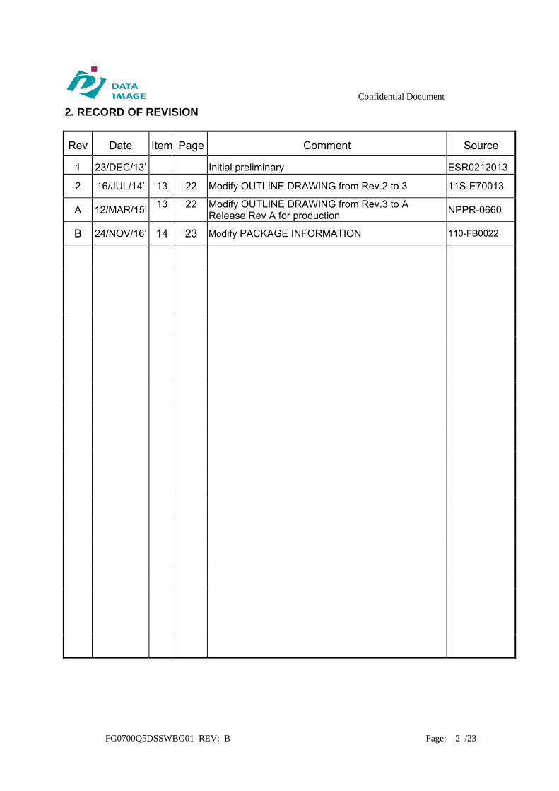
2. RECORD OF REVISION
Rev Date Item Page Comment Source
1 23/DEC/13’ Initial preliminary ESR0212013
2 16/JUL/14’ 13 22 Modify OUTLINE DRAWING from Rev.2 to 3 11S-E70013
A 12/MAR/15’ 13
22
Modify OUTLINE DRAWING from Rev.3 to A Release Rev A for production
NPPR-0660
B 24/NOV/16’ 14 23 Modify PACKAGE INFORMATION 110-FB0022
Confidential Document
FG0700Q5DSSWBG01 REV: B Page: 3 /23
3. GENERAL SPECIFICATIONS
Parameter Specifications Unit Screen Size 7 (diagonal) inch Display Format 800(H) x (R,G,B) x 480(V) dot Active Area 154.08(H) x 85.92(V) mm Pixel Pitch 0.1926 (H) x 0.1790 (V) mm Pixel Configuration RGB Stripe Outline Dimension 165(W) x 100(H) x 5.8 (D) mm Surface treatment Anti-glare Back-light LED Display mode Normally white Weight 155 g View Angle direction 6 o’clock Our components and processes are compliant to RoHS standard 4. ABSOLUTE MAXIMUM RATINGS
GND=0V
Parameter Symbol MIN. MAX. Unit Remark
Power Voltage
DVDD -0.3 5.0 V
Ta=25C AVDD 6.5 13.5 V
VGH -0.3 40.0 V
VGL -20.0 0.3 V
Operating temperature Top -20 70 C Module surface*
Storage temperature Tst -30 80 C -
5. ELECTRICAL CHARACTERISTICS
5.1 Operating Conditions
Parameter Symbol MIN. Typ. MAX. Unit Remark
Power Voltage
DVDD 3.0 3.3 3.6 V Note 2
AVDD 10.2 10.4 10.6 V
VGH 15.3 16.0 16.7 V
VGL -7.7 -7.0 -6.3 V
Input signal voltage VCOM 3.6 3.8 4.0 V Note 4
Input H/L level voltage VIH 0.7 DVDD -- DVDD V
Note 3 VIL 0 -- 0.3 DVDD V
Note 1: Be sure to apply DVDD and VGL to the LCD first, and then apply VGH. Note 2: DVDD setting should match the signals output voltage (refer to Note 3) of customer’s system
board. Note 3: DCLK,HS,VS,RESET,U/D, L/R,DE,R0~R7,G0~G7,B0~B7,MODE,DITHB
Note 4: Typical VCOM is only a reference value. It must be optimized according to each LCM. Please use
VR and base on below application circuit.
Confidential Document
FG0700Q5DSSWBG01 REV: B Page: 4 /23
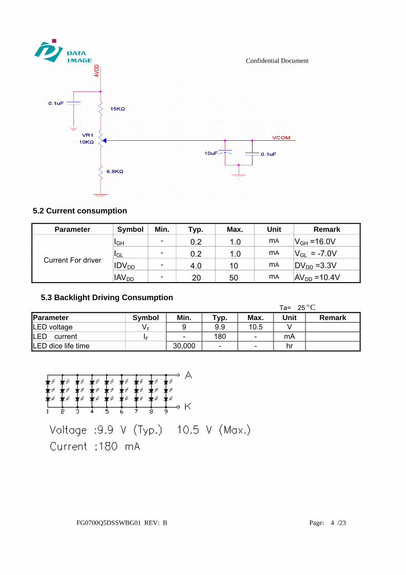
5.2 Current consumption
Parameter Symbol Min. Typ. Max. Unit Remark
Current For driver
IGH - 0.2 1.0 mA VGH =16.0V
IGL - 0.2 1.0 mA VGL = -7.0V
IDVDD - 4.0 10 mA DVDD =3.3V
IAVDD - 20 50 mA AVDD =10.4V
5.3 Backlight Driving Consumption Ta= 25 C
Parameter Symbol Min. Typ. Max. Unit Remark LED voltage VF 9 9.9 10.5 V LED current IF - 180 - mA LED dice life time 30,000 - - hr
Confidential Document
FG0700Q5DSSWBG01 REV: B Page: 5 /23
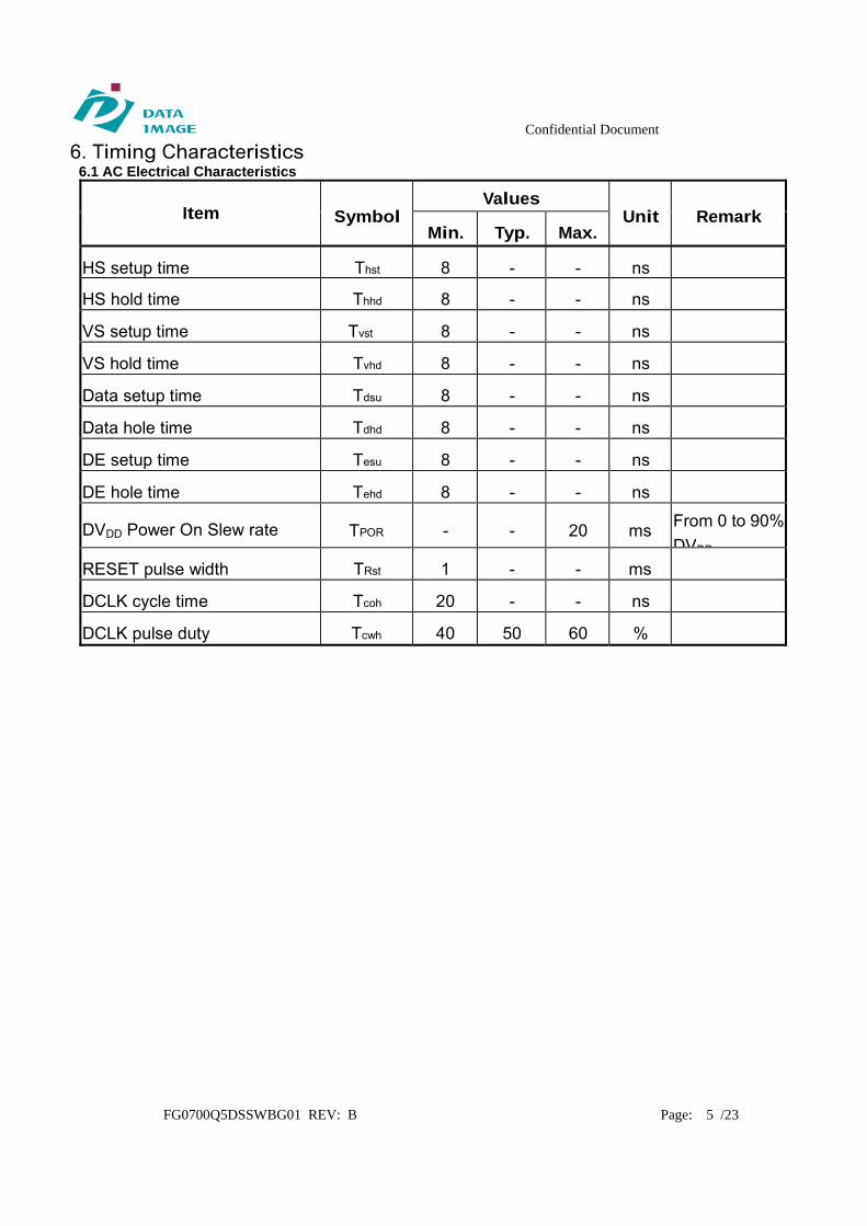
6. Timing Characteristics 6.1 AC Electrical Characteristics
Item SymbolValues
Unit Remark Min. Typ. Max.
HS setup time Thst 8 - - ns
HS hold time Thhd 8 - - ns
VS setup time Tvst 8 - - ns
VS hold time Tvhd 8 - - ns
Data setup time Tdsu 8 - - ns
Data hole time Tdhd 8 - - ns
DE setup time Tesu 8 - - ns
DE hole time Tehd 8 - - ns
DVDD Power On Slew rate
TPOR
-
-
20
ms From 0 to 90%
DVDD
RESET pulse width TRst 1 - - ms
DCLK cycle time Tcoh 20 - - ns
DCLK pulse duty Tcwh 40 50 60 %
Confidential Document
FG0700Q5DSSWBG01 REV: B Page: 6 /23
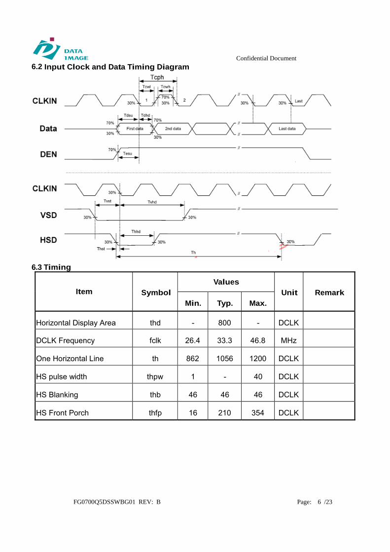
6.2 Input Clock and Data Timing Diagram
6.3 Timing
Item
Symbol Values
Unit
Remark
Min. Typ. Max.
Horizontal Display Area
thd - 800 - DCLK
DCLK Frequency
fclk 26.4 33.3 46.8 MHz
One Horizontal Line
th 862 1056 1200 DCLK
HS pulse width
thpw 1 - 40 DCLK
HS Blanking
thb 46 46 46 DCLK
HS Front Porch
thfp 16 210 354 DCLK
Confidential Document
FG0700Q5DSSWBG01 REV: B Page: 7 /23
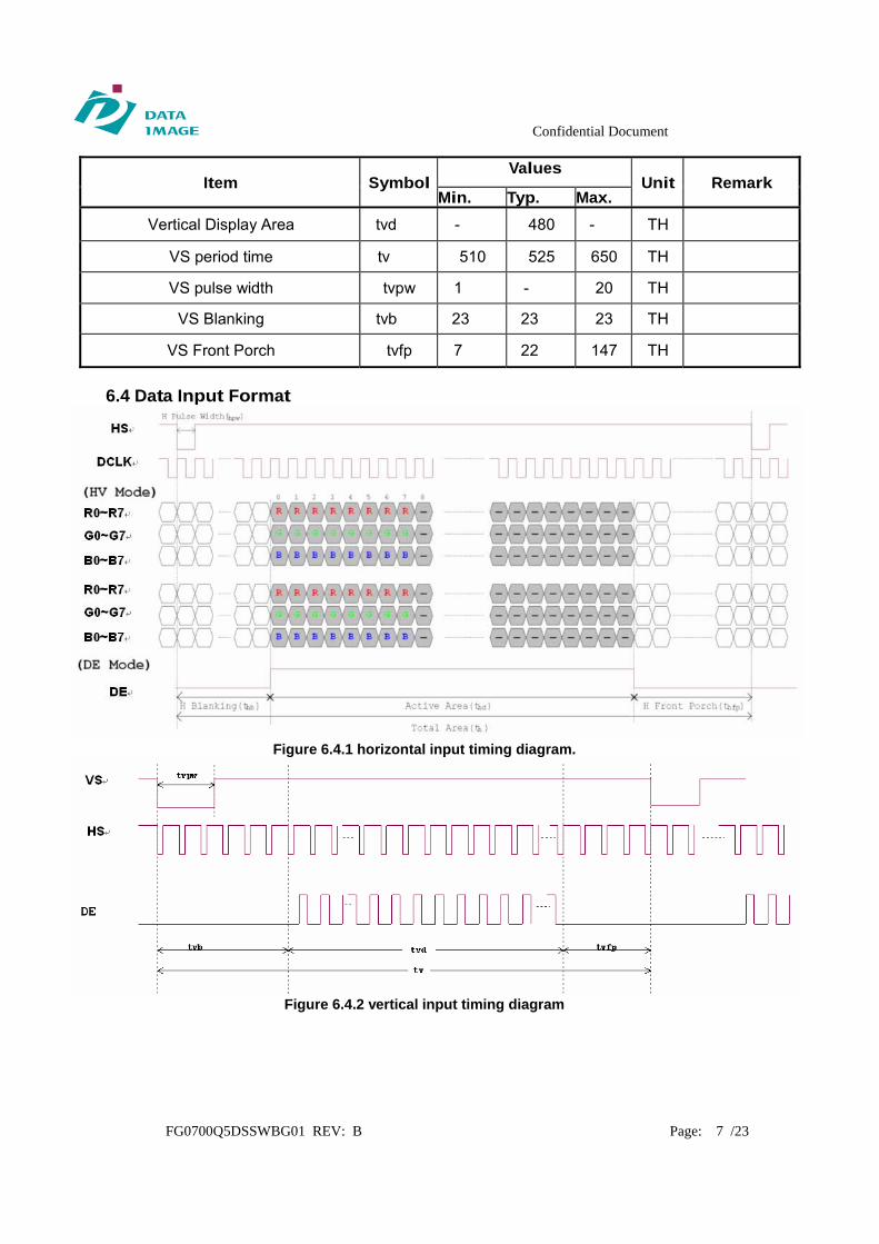
Item SymbolValues
Unit Remark Min. Typ. Max.
Vertical Display Area tvd - 480 - TH
VS period time tv 510 525 650 TH
VS pulse width tvpw 1 - 20 TH
VS Blanking tvb 23 23 23 TH
VS Front Porch tvfp 7 22 147 TH
6.4 Data Input Format
Figure 6.4.1 horizontal input timing diagram.
Figure 6.4.2 vertical input timing diagram
Confidential Document
FG0700Q5DSSWBG01 REV: B Page: 8 /23
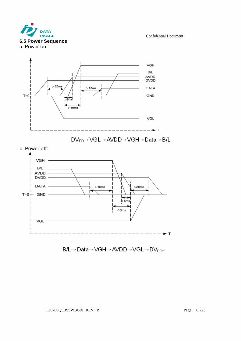
6.5 Power Sequence a. Power on:
b. Power off:
Confidential Document
FG0700Q5DSSWBG01 REV: B Page: 9 /23
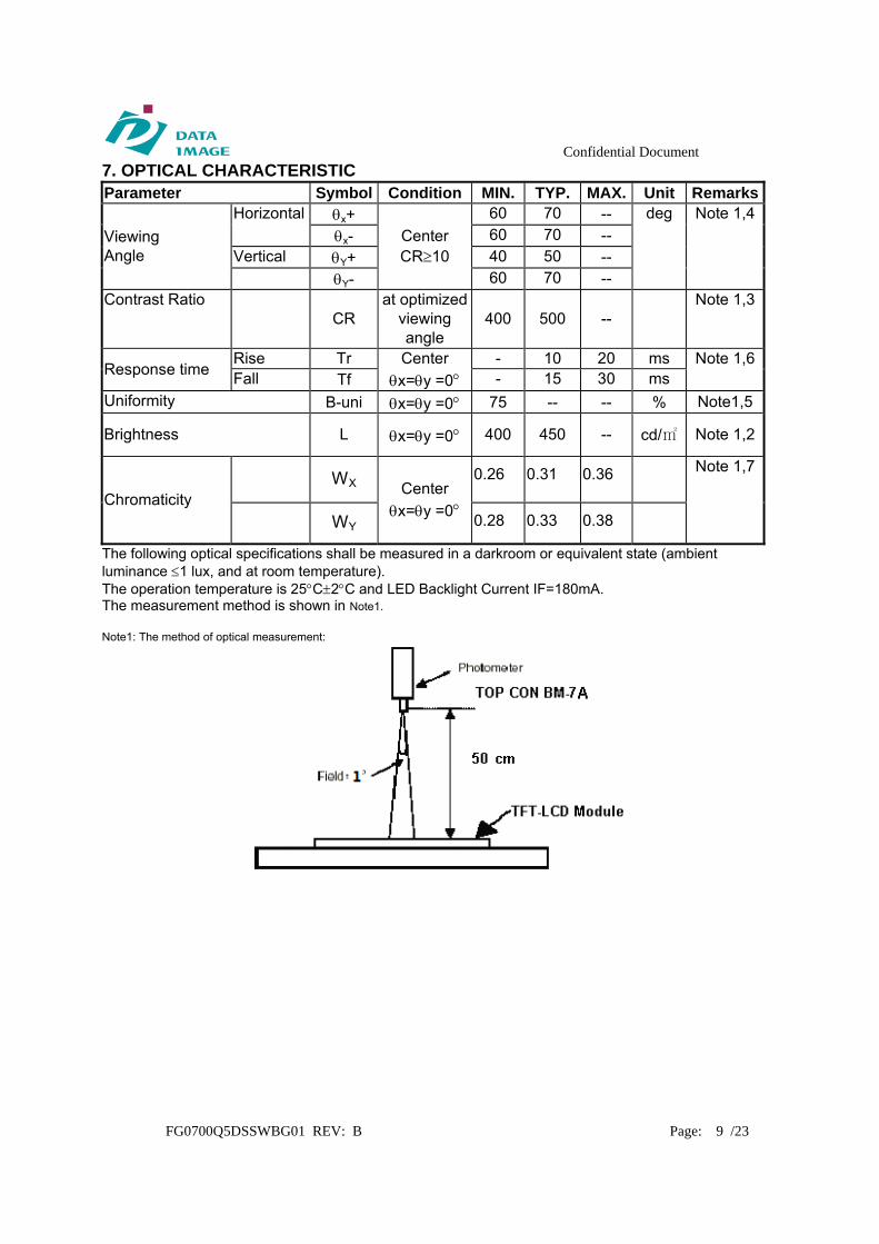
7. OPTICAL CHARACTERISTIC Parameter Symbol Condition MIN. TYP. MAX. Unit Remarks
Viewing Angle
Horizontal x+ Center CR10
60 70 -- deg Note 1,4
x- 60 70 -- Vertical Y+ 40 50 -- Y- 60 70 --
Contrast Ratio CR
at optimized viewing angle
400 500 -- Note 1,3
Response time Rise Tr Center
x=y =0- 10 20 ms Note 1,6
Fall Tf - 15 30 ms
Uniformity B-uni x=y =0 75 -- -- % Note1,5
Brightness L x=y =0 400 450 -- cd/ Note 1,2
Chromaticity
WX
Center
x=y =0
0.26 0.31 0.36 Note 1,7
WY 0.28 0.33 0.38
The following optical specifications shall be measured in a darkroom or equivalent state (ambient luminance 1 lux, and at room temperature). The operation temperature is 25C2C and LED Backlight Current IF=180mA. The measurement method is shown in Note1. Note1: The method of optical measurement:
Confidential Document
FG0700Q5DSSWBG01 REV: B Page: 10 /23
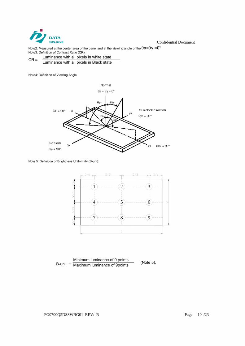
Note2: Measured at the center area of the panel and at the viewing angle of the x=y =0 Note3: Definition of Contrast Ratio (CR):
CR Luminance with all pixels in white state Luminance with all pixels in Black state
Note4: Definition of Viewing Angle
Note 5: Definition of Brightness Uniformity (B-uni):
1 2 3
4 5 6
7 8 9
B-uni = Minimum luminance of 9 points
(Note 5). Maximum luminance of 9points
Confidential Document
FG0700Q5DSSWBG01 REV: B Page: 11 /23
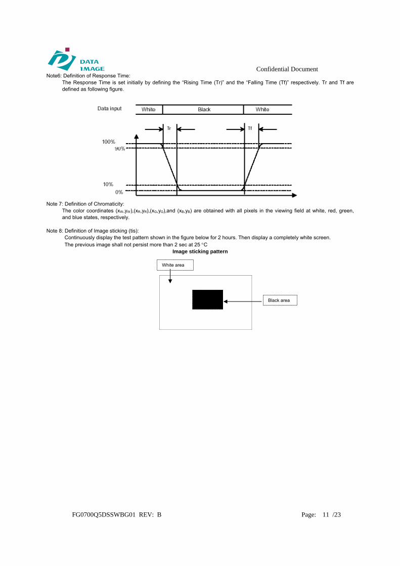
Note6: Definition of Response Time: The Response Time is set initially by defining the “Rising Time (Tr)” and the “Falling Time (Tf)” respectively. Tr and Tf are defined as following figure.
Note 7: Definition of Chromaticity:
The color coordinates (xW,yW),(xR,yR),(xG,yG),and (xB,yB) are obtained with all pixels in the viewing field at white, red, green, and blue states, respectively.
Note 8: Definition of Image sticking (tis): Continuously display the test pattern shown in the figure below for 2 hours. Then display a completely white screen. The previous image shall not persist more than 2 sec at 25 C
Image sticking pattern
White area
Black area
Confidential Document
FG0700Q5DSSWBG01 REV: B Page: 12 /23
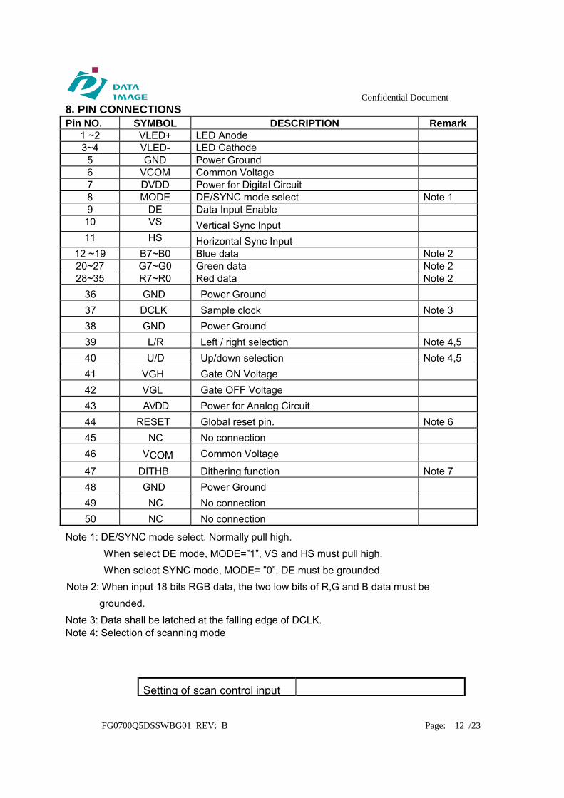
8. PIN CONNECTIONS Pin NO. SYMBOL DESCRIPTION Remark
1 ~2 VLED+ LED Anode 3~4 VLED- LED Cathode
5 GND Power Ground 6 VCOM Common Voltage 7 DVDD Power for Digital Circuit 8 MODE DE/SYNC mode select Note 1 9 DE Data Input Enable
10 VS Vertical Sync Input 11 HS Horizontal Sync Input
12 ~19 B7~B0 Blue data Note 2 20~27 G7~G0 Green data Note 2 28~35 R7~R0 Red data Note 2
36 GND Power Ground
37 DCLK Sample clock Note 3
38 GND Power Ground
39 L/R Left / right selection Note 4,5
40 U/D Up/down selection Note 4,5
41 VGH Gate ON Voltage
42 VGL Gate OFF Voltage
43 AVDD Power for Analog Circuit
44 RESET Global reset pin. Note 6
45 NC No connection
46 VCOM Common Voltage
47 DITHB Dithering function Note 7
48 GND Power Ground
49 NC No connection
50 NC No connection
Note 1: DE/SYNC mode select. Normally pull high.
When select DE mode, MODE=”1”, VS and HS must pull high.
When select SYNC mode, MODE= ”0”, DE must be grounded.
Note 2: When input 18 bits RGB data, the two low bits of R,G and B data must be
grounded.
Note 3: Data shall be latched at the falling edge of DCLK. Note 4: Selection of scanning mode
Setting of scan control input
Confidential Document
FG0700Q5DSSWBG01 REV: B Page: 13 /23
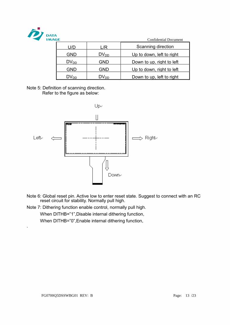
U/D L/R Scanning direction
GND DVDD Up to down, left to right
DVDD GND Down to up, right to left
GND GND Up to down, right to left
DVDD DVDD Down to up, left to right
Note 5: Definition of scanning direction.
Refer to the figure as below:
Note 6: Global reset pin. Active low to enter reset state. Suggest to connect with an RC
reset circuit for stability. Normally pull high.
Note 7: Dithering function enable control, normally pull high.
When DITHB=”1”,Disable internal dithering function,
When DITHB=”0”,Enable internal dithering function, .
Confidential Document
FG0700Q5DSSWBG01 REV: B Page: 14 /23
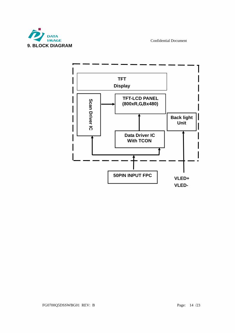
9. BLOCK DIAGRAM
TFT-LCD PANEL (800xR,G,Bx480)
Data Driver IC With TCON
Scan
Driver IC
TFT
Display
VLED+
VLED-
Back light Unit
50PIN INPUT FPC
Confidential Document
FG0700Q5DSSWBG01 REV: B Page: 15 /23
10. QUALITY ASSURANCE 10.1 Test Condition
10.1.1 Temperature and Humidity(Ambient Temperature)
Temperature : 25 5C Humidity : 65 5%
10.1.2 Operation
Unless specified otherwise, test will be conducted under function state.
10.1.3 Container Unless specified otherwise, vibration test will be conducted to the product itself without putting it in a container.
10.1.4 Test Frequency
In case of related to deterioration such as shock test. It will be conducted only
once.
10.1.5 Test Method
No. Reliability Test Item Test Level Remark 1 High Temperature Storage Test T=80 ,240hrs IEC68-2-2 2 Low Temperature Storage Test T=-30 ,240hrs IEC68-2-1 3 High Temperature Operation Test T=70 ,240hrs IEC68-2-2 4 Low Temperature Operation Test T=-20 ,240hrs IEC68-2-1
5 High Temperature and High Humidity Operation Test
T=60 ,90 %RH,240hrs IEC68-2-3
6 Thermal Cycling Test (No operation)
- 30 → +25 → +80 ,200 Cycles 30 min 5 min 30 min
IEC68-2-14
7 Vibration test
Frequency:10~55HZ Amplitude:1.5mm Sweep time:11min Test period:6Cycles for each direction of X,Y,Z
IEC68-2-6
8 Shock test 100G 6ms,±X, ±Y, ±Z 3 times for each direction
IEC68-2-27
9 Drop test Height:60 cm 1 corner, 3 edges, 6 surfaces
IEC68-2-32
10 ESD test
State: operating Location: LCM/TP surface Condition:150pf 330Ω Contact +/- 8kV Air +/-15kV Criteria: Class C
IEC61000-4-2
Confidential Document
FG0700Q5DSSWBG01 REV: B Page: 16 /23
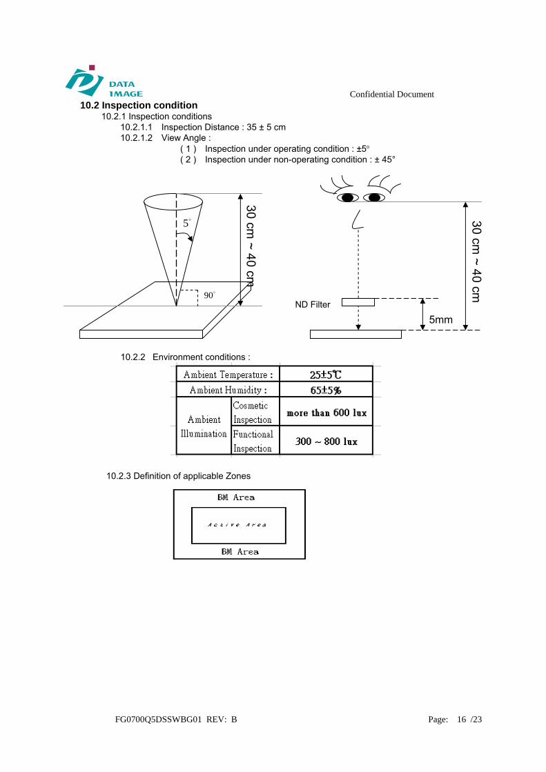
10.2 Inspection condition 10.2.1 Inspection conditions
10.2.1.1 Inspection Distance : 35 ± 5 cm 10.2.1.2 View Angle :
( 1 ) Inspection under operating condition : ±5 ( 2 ) Inspection under non-operating condition : ± 45°
10.2.2 Environment conditions :
10.2.3 Definition of applicable Zones
5mm
ND Filter
30 cm ~
40 cm
5°
90° 30 cm
~ 40 cm
Confidential Document
FG0700Q5DSSWBG01 REV: B Page: 17 /23
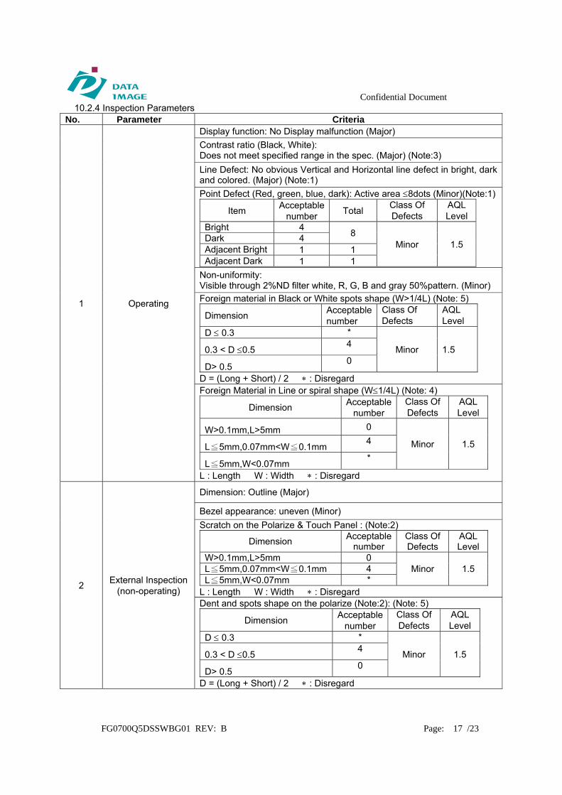
10.2.4 Inspection Parameters No. Parameter Criteria
1 Operating
Display function: No Display malfunction (Major)
Contrast ratio (Black, White): Does not meet specified range in the spec. (Major) (Note:3)
Line Defect: No obvious Vertical and Horizontal line defect in bright, dark and colored. (Major) (Note:1)
Point Defect (Red, green, blue, dark): Active area 8dots (Minor)(Note:1)
Item Acceptable
number Total
Class Of Defects
AQL Level
Bright 4 8
Minor 1.5 Dark 4 Adjacent Bright 1 1 Adjacent Dark 1 1
Non-uniformity: Visible through 2%ND filter white, R, G, B and gray 50%pattern. (Minor)
Foreign material in Black or White spots shape (W>1/4L) (Note: 5)
Dimension Acceptable number
Class Of Defects
AQL Level
D 0.3 *
Minor 1.5 0.3 < D 0.5 4
D> 0.5 0
D = (Long + Short) / 2 : Disregard Foreign Material in Line or spiral shape (W1/4L) (Note: 4)
Dimension Acceptable
number Class Of Defects
AQL Level
W>0.1mm,L>5mm 0
Minor 1.5 L≦5mm,0.07mm<W≦0.1mm 4
L≦5mm,W<0.07mm *
L : Length W : Width : Disregard
2 External Inspection
(non-operating)
Dimension: Outline (Major)
Bezel appearance: uneven (Minor)
Scratch on the Polarize & Touch Panel : (Note:2)
Dimension Acceptable
number Class Of Defects
AQL Level
W>0.1mm,L>5mm 0 Minor 1.5 L≦5mm,0.07mm<W≦0.1mm 4
L≦5mm,W<0.07mm * L : Length W : Width : Disregard Dent and spots shape on the polarize (Note:2): (Note: 5)
Dimension Acceptable
number Class Of Defects
AQL Level
D 0.3 *
Minor 1.5 0.3 < D 0.5 4
D> 0.5 0
D = (Long + Short) / 2 : Disregard
Confidential Document
FG0700Q5DSSWBG01 REV: B Page: 18 /23
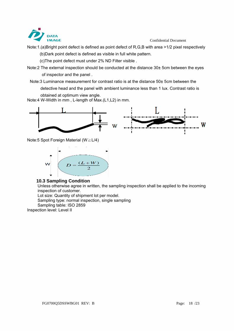
Note:1.(a)Bright point defect is defined as point defect of R,G,B with area >1/2 pixel respectively
(b)Dark point defect is defined as visible in full white pattern.
(c)The point defect must under 2% ND Filter visible .
Note:2 The external inspection should be conducted at the distance 30± 5cm between the eyes
of inspector and the panel .
Note:3 Luminance measurement for contrast ratio is at the distance 50± 5cm between the
detective head and the panel with ambient luminance less than 1 lux. Contrast ratio is
obtained at optimum view angle. Note:4 W-Width in mm , L-length of Max.(L1,L2) in mm.
Note:5 Spot Foreign Material (W≧L/4)
10.3 Sampling Condition
Unless otherwise agree in written, the sampling inspection shall be applied to the incoming inspection of customer.
Lot size: Quantity of shipment lot per model. Sampling type: normal inspection, single sampling Sampling table: ISO 2859 Inspection level: Level II
Confidential Document
FG0700Q5DSSWBG01 REV: B Page: 19 /23
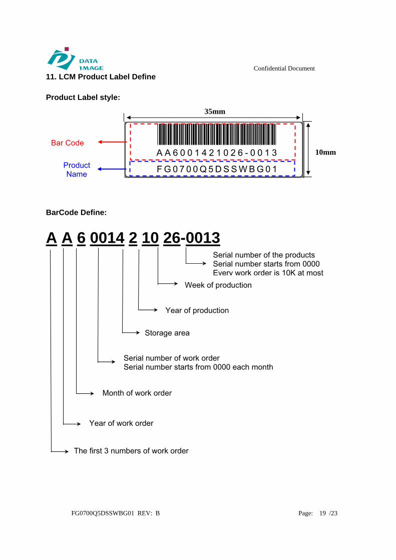
11. LCM Product Label Define
Product Label style:
BarCode Define:
A A 6 0014 2 10 26-0013
A A 6 0 0 1 4 2 1 0 2 6 - 0 0 1 3
F G 0 7 0 0 Q 5 D S S W B G 0 1
35mm
10mm Bar Code
Product Name
The first 3 numbers of work order
Year of work order
Month of work order
Serial number of work order Serial number starts from 0000 each month
Storage area
Serial number of the products Serial number starts from 0000 Every work order is 10K at most
Year of production
Week of production
Confidential Document
FG0700Q5DSSWBG01 REV: B Page: 20 /23
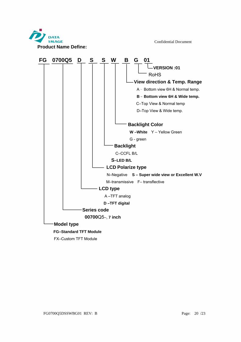
Product Name Define:
FG 0700Q5 D S S W B G 01
VERSION :01
RoHS
View direction & Temp. Range
A– Bottom view 6H & Normal temp.
B– Bottom view 6H & Wide temp.
C–Top View & Normal temp
D–Top View & Wide temp.
Backlight Color
W –White Y – Yellow Green
G - green
Backlight
C–CCFL B/L
S–LED B/L
LCD Polarize type
N–Negative S – Super wide view or Excellent W.V
M–transmissive F– transflective
LCD type
A –TFT analog
D –TFT digital
Series code
00700Q5–, 7 inch
Model type
FG–Standard TFT Module
FX–Custom TFT Module
Confidential Document
FG0700Q5DSSWBG01 REV: B Page: 21 /23
12. PRECAUTIONS IN USE LCM
1. ASSEMBLY PRECAUTIONS (1) You must mount a module using holes arranged in
four corners or four sides. (2) You should consider the mounting structure so that
uneven force (ex. Twisted stress) is not applied to the module. And the case on which a module is mounted should have sufficient strength so that external force is not transmitted directly to the module.
(3) Do not touch, push or rub the exposed polarizers with glass, tweezers or anything harder than HB pencil lead. And please do not rub with dust clothes with chemical treatment.
(4) Wipe off saliva or water drops as soon as possible. Their long time contact with polarizer causes deformations and color fading.
(5) Do not open the case because inside circuits do not have sufficient strength.
(6) Please do not take a LCD module to pieces and reconstruct it. Resolving and reconstructing modules may cause them not to work well.
(7) Please do not touch metal frames with bare hands and soiled gloves. A color change of the metal frames can happen during a long preservation of soiled LCD modules.
(8) Please pay attention to handling lead wire of backlight so that it is not tugged in connecting with inverter.
2. OPERATING PRECAUTIONS (1) Please be sure to turn off the power supply before
connecting and disconnecting signal input cable. (2) Please do not change variable resistance settings in
LCD module. They are adjusted to the most suitable value. If they are changed, it might happen LCD does not satisfy the characteristics specification
(3) Be careful for condensation at sudden temperature change. Condensation makes damage to polarizer or electrical contacted parts. And after fading condensation, smear or spot will occur.
(4) When fixed patterns are displayed for a long time, remnant image is likely to occur.
(5) Module has high frequency circuits. Sufficient suppression to the electromagnetic interference shall be done by system manufacturers. Grounding and shielding methods may be important to minimize the interference.
(6) Please consider that LCD backlight takes longer time to become stable of radiation characteristics in low temperature than in room temperature.
3. ELECTROSTATIC DISCHARGE CONTROL (1) The operator should be grounded whenever he/she
comes into contact with the module. Never touch any of the conductive parts such the copper leads on the PCB and the interface terminals with any
parts of the human body. (2) The modules should be kept in antistatic bags or
other containers resistant to static for storage. (3) Only properly grounded soldering irons should be
used. (4) If an electric screwdriver is used, it should be well
grounded and shielded from commutator sparks. (5) The normal static prevention measures should be
observed for work clothes and working benches; for the latter conductive (rubber) mat is recommended
(6) Since dry air is inductive to statics, a relative humidity of 50-60% is recommended.
4. STORAGE PRECAUTIONS (1) When you store LCDs for a long time, it is
recommended to keep the temperature between 0°C-40°C without the exposure of sunlight and to keep the humidity less than 90%RH.
(2) Please do not leave the LCDs in the environment of high humidity and high temperature such as 60°C 90%RH
(3) Please do not leave the LCDs in the environment of low temperature; below -20°C.
5. OTHERS (1) A strong incident light into LCD panel might cause
display characteristics' changing inferior because of polarizer film, color filter, and other materials becoming inferior. Please do not expose LCD module direct sunlight Land strong UV rays
(2) Please pay attention to a panel side of LCD module not to contact with other materials in preserving it alone.
(3) For the packaging box, please pay attention to the followings:
(4) Please do not pile them up more than 5 boxes. (They are not designed so.) And please do not turn over.
(5) Please handle packaging box with care not to give them sudden shock and vibrations. And also please do not throw them up.
(6) Packing box and inner case for LCDs are made of cardboard. So please pay attention not to get them wet. (Such like keeping them in high humidity or wet place can occur getting them wet.)
6. LIMITED WARRANTY Unless otherwise agreed between DATA IMAGE and customer, DATA IMAGE will replace or repair any of its LCD and LCM which is found to be defective electrically and visually when inspected in accordance with DATA IMAGE acceptance standards, for a period on one year from date of shipment. Confirmation of such date shall be based on freight documents. The warranty liability of DATA IMAGE is limited to repair and/or replacement on the terms set forth above. DATA IMAGE will not responsible for any subsequent or consequential events.
Confidential Document
FG0700Q5DSSWBG01 REV: B Page: 22 /23
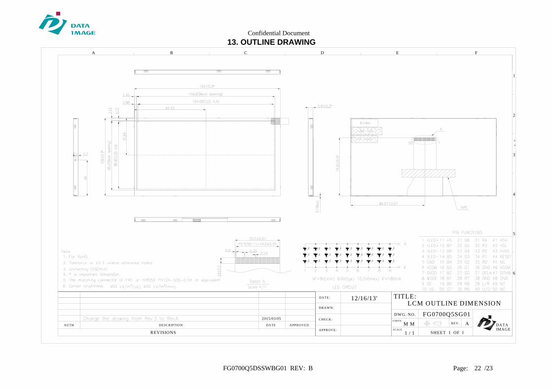
13. OUTLINE DRAWING
2015/03/05
A
FG0700Q5SG01
LCM OUTLINE DIMENSION
K
A
F
2
3
4
1
EDC
5
6
DATAIMAGE
REV.
1SHEET OFSCALE
UNITS
TITLE:
DWG. NO.
1 / 1
M M
DRAWN:
DATE:
APPROVE:
CHECK:
DATE APPROVED
1
BA
DESCRIPTION
REVISIONS
AUTH
12/16/13'
Confidential Document
FG0700Q5DSSWBG01 REV: B Page: 23 /23
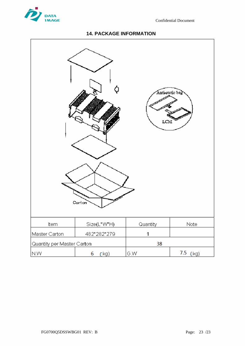
14. PACKAGE INFORMATION