darpa workshop wdm for military platforms april 18, 2000 … · optical switches low threshold...
TRANSCRIPT

Honeywell Technology CenterHoneywell Technology Center1APPROVED FOR PUBLIC RELEASE, DISTRIBUTION UNLIMITED
REVIEW OF THIS MATERIAL DOES NOT IMPLY DEPARTMENT OFDEFENSE INDORSEMENT OF FACTUAL ACCURACY OR OPINION
DARPA WorkshopWDM for Military Platforms
April 18, 2000
Robust WDM Components, Packaging, and Integration
Mary Hibbs-BrennerHoneywell Technology Center
Outline• Application/System Level Motivation
• military• commercial
• Requirements• Technology Enablers

Report Documentation Page Form ApprovedOMB No. 0704-0188
Public reporting burden for the collection of information is estimated to average 1 hour per response, including the time for reviewing instructions, searching existing data sources, gathering andmaintaining the data needed, and completing and reviewing the collection of information. Send comments regarding this burden estimate or any other aspect of this collection of information,including suggestions for reducing this burden, to Washington Headquarters Services, Directorate for Information Operations and Reports, 1215 Jefferson Davis Highway, Suite 1204, ArlingtonVA 22202-4302. Respondents should be aware that notwithstanding any other provision of law, no person shall be subject to a penalty for failing to comply with a collection of information if itdoes not display a currently valid OMB control number.
1. REPORT DATE 18 APR 2000
2. REPORT TYPE N/A
3. DATES COVERED -
4. TITLE AND SUBTITLE Robust WDM Components, Packaging and Integration
5a. CONTRACT NUMBER
5b. GRANT NUMBER
5c. PROGRAM ELEMENT NUMBER
6. AUTHOR(S) 5d. PROJECT NUMBER
5e. TASK NUMBER
5f. WORK UNIT NUMBER
7. PERFORMING ORGANIZATION NAME(S) AND ADDRESS(ES) Honeywell Technology Center
8. PERFORMING ORGANIZATIONREPORT NUMBER
9. SPONSORING/MONITORING AGENCY NAME(S) AND ADDRESS(ES) 10. SPONSOR/MONITOR’S ACRONYM(S)
11. SPONSOR/MONITOR’S REPORT NUMBER(S)
12. DISTRIBUTION/AVAILABILITY STATEMENT Approved for public release, distribution unlimited
13. SUPPLEMENTARY NOTES DARPA/MTO, WDM for Military Platforms Workshop held in McLean, VA on April 18-19, 2000, Theoriginal document contains color images.
14. ABSTRACT
15. SUBJECT TERMS
16. SECURITY CLASSIFICATION OF: 17. LIMITATION OF ABSTRACT
UU
18. NUMBEROF PAGES
16
19a. NAME OFRESPONSIBLE PERSON
a. REPORT unclassified
b. ABSTRACT unclassified
c. THIS PAGE unclassified
Standard Form 298 (Rev. 8-98) Prescribed by ANSI Std Z39-18

Honeywell Technology CenterHoneywell Technology Center2APPROVED FOR PUBLIC RELEASE, DISTRIBUTION UNLIMITED
REVIEW OF THIS MATERIAL DOES NOT IMPLY DEPARTMENT OFDEFENSE INDORSEMENT OF FACTUAL ACCURACY OR OPINION
Applications and System Motivation
• Multi-sensor networks• Military: flight control• Commercial: controlling critical environments
• Security: use multiple wavelengths to ensure channel separation
• Interconnects• Military: increased reliability via reduced number of connectors• Commercial: 10 Gbps Ethernet and beyond

Honeywell Technology CenterHoneywell Technology Center3APPROVED FOR PUBLIC RELEASE, DISTRIBUTION UNLIMITED
REVIEW OF THIS MATERIAL DOES NOT IMPLY DEPARTMENT OFDEFENSE INDORSEMENT OF FACTUAL ACCURACY OR OPINION
Likelihood of Commercial Volumes for WDM
Coarse WDM proposed to IEEE 802.3ae committeefor 10 Gbps Ethernet
• multimode fiber to minimize cost over short distances(100 - 300m)
• both 850nm and 1300nm proposals
• 4 channels at 3.125 Gbps

Honeywell Technology CenterHoneywell Technology Center4APPROVED FOR PUBLIC RELEASE, DISTRIBUTION UNLIMITED
REVIEW OF THIS MATERIAL DOES NOT IMPLY DEPARTMENT OFDEFENSE INDORSEMENT OF FACTUAL ACCURACY OR OPINION
Optically Addressed Sensor NetworksOptically Addressed Sensor Networks• The need:
– Vehicle management systems/condition based maintenance systems requiremany sensors, with hundreds of pounds of associated wiring
– Sensors need to tolerate high temperatures, electrically noisy environments– Sensing multiple parameters (temperature, strain, vibration, etc.), widely
distributed across vehicle• Mission benefits of optically addressed sensor networks
– Condition based maintenance-improved maintenance efficiency, reduceddowntime, increased safety
– Reduced weight means increased range/fly time for UAVs– Improved vehicle performance and maneuverability with improved flight control

Honeywell Technology CenterHoneywell Technology Center5APPROVED FOR PUBLIC RELEASE, DISTRIBUTION UNLIMITED
REVIEW OF THIS MATERIAL DOES NOT IMPLY DEPARTMENT OFDEFENSE INDORSEMENT OF FACTUAL ACCURACY OR OPINION
Optically Addressed Sensor NetworksOptically Addressed Sensor Networks
1. ORIMS for wide temperature range operation 2. Optical fiber networks allow remoting of temperature sensitive
optoelectronics and electronics3. WDM allows reduction in number of cables
4. Optical couplers for interfacing with sensors and for networking (diffractive and/or integrated optics)
5. Fiber network design (built-in redundancy and temperature compatibility)

Honeywell Technology CenterHoneywell Technology Center6APPROVED FOR PUBLIC RELEASE, DISTRIBUTION UNLIMITED
REVIEW OF THIS MATERIAL DOES NOT IMPLY DEPARTMENT OFDEFENSE INDORSEMENT OF FACTUAL ACCURACY OR OPINION
MEMS and WDM Photonics TechnologyMEMS and WDM Photonics TechnologyEnable Optically Addressed Sensor NetworksEnable Optically Addressed Sensor Networks
Polysilicon ShellUpper Cavity
Microbeam
Lower Cavity
Applied Strain
OpticalFiber
EmbeddedPhotodiode
MEMS: Optical Resonant Microsensors
• Flexibility - multiple sensor types - plug-and-play potential - expandable
• No electronics or power at sensor node - non-incendiary - compatible to harsh environments - EMI immunity at sensor - reduced sensor node cost
Optical WDM networks
• Reduced cabling weight and volume• Wavelength routes to a node, frequency domain used to distinguish different at node
Amp
DC
DC
AC
λ1
λ2
D1
Output
.....
1 2 N
NxN Star Coupler
STORMSensors
Optical Fiber
STORM Chip
λ1
Silicon DiaphragmMicrobeam
Optical Network
Sensor

Honeywell Technology CenterHoneywell Technology Center7APPROVED FOR PUBLIC RELEASE, DISTRIBUTION UNLIMITED
REVIEW OF THIS MATERIAL DOES NOT IMPLY DEPARTMENT OFDEFENSE INDORSEMENT OF FACTUAL ACCURACY OR OPINION
Networked Photonic Sensing
• Uses network topology androuting concepts
• More powerful concept than multiplexing yet simpler to apply and more flexible.
• Usable with virtually alloptical sensor types
• Expandable design with ability to lowercost of sensing by a factorof 10 to a 100!
• Takes advantage of emerging“all optical” network technologyand components

Honeywell Technology CenterHoneywell Technology Center8APPROVED FOR PUBLIC RELEASE, DISTRIBUTION UNLIMITED
REVIEW OF THIS MATERIAL DOES NOT IMPLY DEPARTMENT OFDEFENSE INDORSEMENT OF FACTUAL ACCURACY OR OPINION
Critical Spaces Applications
• Laboratories and General Spaces– Hazardous gas, VOC, bacteria detection– Demand controlled ventilation– Automatic (and repeatable) fume hood containment testing– Room occupancy detection (CO2)– Room and duct static pressure measurement
• Animal Research Facilities– Detection of allergens (ammonia)
• Clean Rooms– On-line particulate monitoring
Honeywell Technology CenterHoneywell Technology Center9APPROVED FOR PUBLIC RELEASE, DISTRIBUTION UNLIMITED
REVIEW OF THIS MATERIAL DOES NOT IMPLY DEPARTMENT OFDEFENSE INDORSEMENT OF FACTUAL ACCURACY OR OPINION
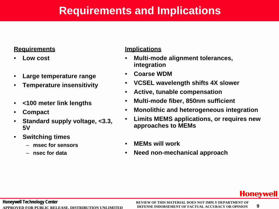
Requirements and Implications
Requirements• Low cost
• Large temperature range• Temperature insensitivity
• <100 meter link lengths• Compact• Standard supply voltage, <3.3,
5V• Switching times
– msec for sensors– nsec for data
Implications• Multi-mode alignment tolerances,
integration• Coarse WDM• VCSEL wavelength shifts 4X slower• Active, tunable compensation• Multi-mode fiber, 850nm sufficient• Monolithic and heterogeneous integration• Limits MEMS applications, or requires new
approaches to MEMs
• MEMs will work• Need non-mechanical approach

Honeywell Technology CenterHoneywell Technology Center10APPROVED FOR PUBLIC RELEASE, DISTRIBUTION UNLIMITED
REVIEW OF THIS MATERIAL DOES NOT IMPLY DEPARTMENT OFDEFENSE INDORSEMENT OF FACTUAL ACCURACY OR OPINION
Candidate Enabling Technologies for WDM
Source 1
Source 2
Source N
…
Receiver 1
…
Receiver 2
Receiver N
fiberMU
XD
eMU
X
Tx/Rx
Tx/Rx
add/dropnode
add/dropnode
• diffractive elements/gratings• photonic bandgap devices• MEMS• VCSEL
• PBG µ µ µ µ-cavity laser• resonant reflective filter• heterogeneous integration
SourcesMUX/DeMUX/Add-Drop
• dielectric filters• resonant reflective filter• photonic bandgap devices• heterogeneous integration
Receivers
Honeywell Technology CenterHoneywell Technology Center11APPROVED FOR PUBLIC RELEASE, DISTRIBUTION UNLIMITED
REVIEW OF THIS MATERIAL DOES NOT IMPLY DEPARTMENT OFDEFENSE INDORSEMENT OF FACTUAL ACCURACY OR OPINION
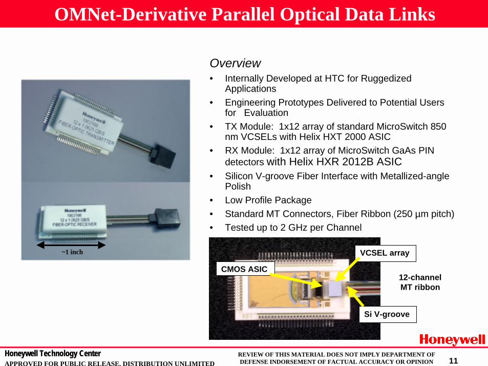
Overview• Internally Developed at HTC for Ruggedized
Applications• Engineering Prototypes Delivered to Potential Users
for Evaluation• TX Module: 1x12 array of standard MicroSwitch 850
nm VCSELs with Helix HXT 2000 ASIC• RX Module: 1x12 array of MicroSwitch GaAs PIN
detectors with Helix HXR 2012B ASIC• Silicon V-groove Fiber Interface with Metallized-angle
Polish• Low Profile Package• Standard MT Connectors, Fiber Ribbon (250 µm pitch)• Tested up to 2 GHz per Channel
VCSEL array
Si V-groove
CMOS ASIC12-channelMT ribbon
~1 inch
OMNet-Derivative Parallel Optical Data Links

Honeywell Technology CenterHoneywell Technology Center12APPROVED FOR PUBLIC RELEASE, DISTRIBUTION UNLIMITED
REVIEW OF THIS MATERIAL DOES NOT IMPLY DEPARTMENT OFDEFENSE INDORSEMENT OF FACTUAL ACCURACY OR OPINION
Smart Pixel Array with Heterogeneous IntegrationSmart Pixel Array with Heterogeneous Integration
4 mm
2D OE array bump-bonded2D OE array bump-bondeddirectly on top of a Si-CMOSdirectly on top of a Si-CMOS
ASIC chipASIC chip
4x4 clusters (64 VCSELs) 4x4 clusters (64 VCSELs) poweredpowered through the AISC through the AISC
850nm VCSEL lights are perceivedas red on a 3-chip CCD camera.
Driver Receiver
Si CMOSSi CMOS
Superstrate
An 256 VCSEL and 256 PD arrayintegrated with a Si-CMOS ASIC.
Four active VCSELsin a unit cell light up,captured by a single-chip CCD camera.
Honeywell Technology CenterHoneywell Technology Center13APPROVED FOR PUBLIC RELEASE, DISTRIBUTION UNLIMITED
REVIEW OF THIS MATERIAL DOES NOT IMPLY DEPARTMENT OFDEFENSE INDORSEMENT OF FACTUAL ACCURACY OR OPINION
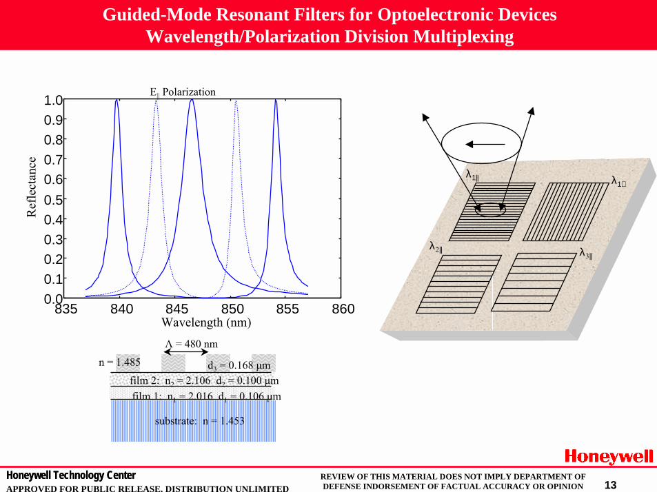
Guided-Mode Resonant Filters for Optoelectronic DevicesWavelength/Polarization Division Multiplexing
λ1⊥λ1||
λ2|| λ3||
Wavelength (nm)835 840 845 850 855 860
0.00.10.20.30.40.50.60.70.80.91.0
Ref
lect
ance
E|| Polarization
film 2: n2 = 2.106 d2 = 0.100 μmfilm 1: n1 = 2.016 d1 = 0.106 μm
substrate: n = 1.453
d3 = 0.168 μmn = 1.485
Λ = 480 nm
Honeywell Technology CenterHoneywell Technology Center14APPROVED FOR PUBLIC RELEASE, DISTRIBUTION UNLIMITED
REVIEW OF THIS MATERIAL DOES NOT IMPLY DEPARTMENT OFDEFENSE INDORSEMENT OF FACTUAL ACCURACY OR OPINION
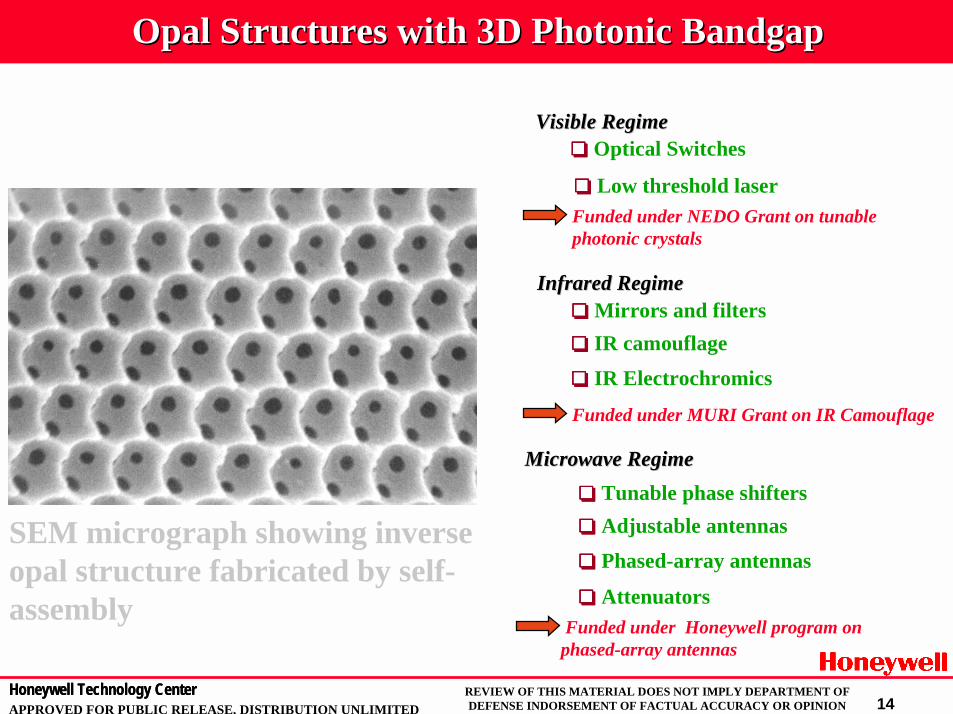
Opal Structures with 3D Photonic BandgapOpal Structures with 3D Photonic Bandgap
SEM micrograph showing inverse opal structure fabricated by self-assembly
Visible RegimeVisible Regime❏❏❏❏ Optical Switches
❏❏❏❏ Low threshold laser Funded under NEDO Grant on tunable photonic crystals
Infrared RegimeInfrared Regime❏❏❏❏ Mirrors and filters❏❏❏❏ IR camouflage❏❏❏❏ IR Electrochromics
Funded under MURI Grant on IR Camouflage
Microwave RegimeMicrowave Regime❏❏❏❏ Tunable phase shifters❏❏❏❏ Adjustable antennas❏❏❏❏ Phased-array antennas
Funded under Honeywell program on phased-array antennas
❏❏❏❏ Attenuators
Honeywell Technology CenterHoneywell Technology Center15APPROVED FOR PUBLIC RELEASE, DISTRIBUTION UNLIMITED
REVIEW OF THIS MATERIAL DOES NOT IMPLY DEPARTMENT OFDEFENSE INDORSEMENT OF FACTUAL ACCURACY OR OPINION
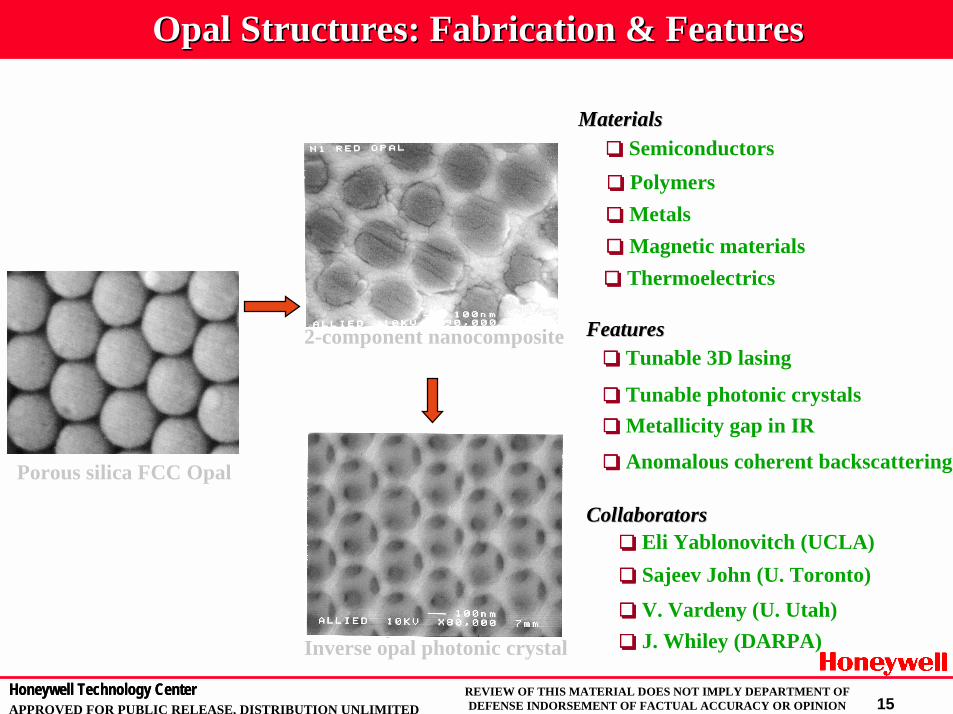
Opal Structures: Fabrication & FeaturesOpal Structures: Fabrication & Features
MaterialsMaterials❏❏❏❏ Semiconductors❏❏❏❏ Polymers❏❏❏❏ Metals
Porous silica FCC Opal
2-component nanocomposite
Inverse opal photonic crystal
❏❏❏❏ Magnetic materials❏❏❏❏ Thermoelectrics
FeaturesFeatures❏❏❏❏ Tunable 3D lasing
❏❏❏❏ Tunable photonic crystals❏❏❏❏ Metallicity gap in IR
❏❏❏❏ Anomalous coherent backscattering
CollaboratorsCollaborators❏❏❏❏ Eli Yablonovitch (UCLA)❏❏❏❏ Sajeev John (U. Toronto)❏❏❏❏ V. Vardeny (U. Utah)❏❏❏❏ J. Whiley (DARPA)

Honeywell Technology CenterHoneywell Technology Center16APPROVED FOR PUBLIC RELEASE, DISTRIBUTION UNLIMITED
REVIEW OF THIS MATERIAL DOES NOT IMPLY DEPARTMENT OFDEFENSE INDORSEMENT OF FACTUAL ACCURACY OR OPINION
Summary
• Transition of optoelectronics from telecom to datacom required technology development
• The same will be true for WDM for LANs and SANs
• Military applications may leverage commercial CWDMbut will have special reliability and ruggedization req’ts
• Widespread Acceptance Requires both Cost Reduction and Volume→→→→ technology development