dac5672 14-bit 275 msps digital-to-analog converter · • medical and test instrumentation •...
TRANSCRIPT

DE-MUX
DA[13:0]
DB[13:0]
MODE
GSET
Latch A
Latch B 14−b DAC
14−b DACIOUTA1
IOUTA2
IOUTB1
IOUTB2
1.2 V Reference
WRTB WRTA CLKB CLKA
BIASJ_A
BIASJ_B
EXTIO
DVDD DGND AVDD AGND
SLEEP
Product
Folder
Order
Now
Technical
Documents
Tools &
Software
Support &Community
An IMPORTANT NOTICE at the end of this data sheet addresses availability, warranty, changes, use in safety-critical applications,intellectual property matters and other important disclaimers. PRODUCTION DATA.
DAC5672SLAS440D –NOVEMBER 2004–REVISED AUGUST 2017
DAC5672 14-Bit 275 MSPS Digital-to-Analog Converter
1
1 Features1• 14-Bit Dual Transmit Digital-to-Analog Converter
(DAC)• 275 MSPS Update Rate• Single-Supply: 3 V to 3.6 V• High Spurious-Free Dynamic Range (SFDR): 84
dBc at 5 MHz• High Third-Order Two-Tone Intermodulation
(IMD3): 79 dBc at 15.1 MHz and 16.1 MHz• WCDMA Adjacent Channel Leakage Ratio
(ACLR): 78 dB at Baseband• WCDMA ACLR: 73 dB at 30.72 MHz• Independent or Single Resistor Gain Control• Dual or Interleaved Data• On-Chip 1.2-V Reference• Low Power: 330 mW• Power-Down Mode: 9 mW• Package: 48-Pin Thin-Quad Flat Pack (TQFP)
2 Applications• Cellular Base Transceiver Station Transmit
Channel– CDMA: W-CDMA, CDMA2000, IS-95– TDMA: GSM, IS-136, EDGE and UWC-136
• Medical and Test Instrumentation• Arbitrary Waveform Generators (ARB)• Direct Digital Synthesis (DDS)• Cable Modem Termination System (CMTS)
3 DescriptionThe DAC5672 device is a monolithic, dual-channel,14-bit, high-speed DAC with on-chip voltagereference.
Operating with update rates of up to 275 MSPS, theDAC5672 offers exceptional dynamic performance,tight-gain, and offset matching characteristics thatmake the device well-suited in I/Q baseband or directIF communication applications.
Each DAC has a high-impedance, differential-currentoutput suitable for single-ended or differential analog-output configurations. External resistors allow scalingthe full-scale output current for each DAC separatelyor together, typically between 2 mA and 20 mA. Anaccurate on-chip voltage reference is temperature-compensated and delivers a stable 1.2-V referencevoltage. Optionally, an external reference may beused.
The DAC5672 has two, 14-bit, parallel input portswith separate clocks and data latches. For flexibility,the DAC5672 supports multiplexed data for eachDAC on one port when operating in interleavedmode.
The DAC5672 is specifically designed for adifferential transformer-coupled output with a 50-Ωdoubly-terminated load. For a 20-mA full-scale outputcurrent, a 4:1 impedance ratio (resulting in an outputpower of 4 dBm) and 1:1 impedance ratio transformer(–2 dBm output power) are supported.
The DAC5672 is available in a 48-pin TQFP package.Pin compatibility between family members provides12-bit (DAC5662) and 14-bit (DAC5672) resolutions.Furthermore, the DAC5672 is pin compatible to theDAC2904 and AD9767 dual DACs. The device ischaracterized for operation over the industrialtemperature range from –40°C to 85°C.
Device Information(1)
PART NUMBER PACKAGE BODY SIZE (NOM)DAC5672 TQFP (48) 7.00 mm × 7.00 mm
(1) For all available packages, see the orderable addendum atthe end of the data sheet.
Functional Block Diagram

2
DAC5672SLAS440D –NOVEMBER 2004–REVISED AUGUST 2017 www.ti.com
Product Folder Links: DAC5672
Submit Documentation Feedback Copyright © 2004–2017, Texas Instruments Incorporated
Table of Contents1 Features .................................................................. 12 Applications ........................................................... 13 Description ............................................................. 14 Revision History..................................................... 25 Pin Configuration and Functions ......................... 36 Specifications......................................................... 5
6.1 Absolute Maximum Ratings ...................................... 56.2 ESD Ratings.............................................................. 56.3 Recommended Operating Conditions....................... 56.4 Thermal Information .................................................. 66.5 Electrical Characteristics........................................... 66.6 Electrical Characteristics........................................... 76.7 Electrical Characteristics: AC Characteristics........... 76.8 Electrical Characteristics: Digital Characteristics...... 96.9 Switching Characteristics .......................................... 96.10 Typical Characteristics........................................... 9
7 Detailed Description ............................................ 147.1 Overview ................................................................. 14
7.2 Functional Block Diagram ....................................... 147.3 Feature Description................................................. 157.4 Device Functional Modes........................................ 167.5 Programming........................................................... 20
8 Application and Implementation ........................ 228.1 Application Information............................................ 228.2 Typical Application ................................................. 22
9 Power Supply Recommendations ...................... 2410 Layout................................................................... 25
10.1 Layout Guidelines ................................................. 2510.2 Layout Example .................................................... 25
11 Device and Documentation Support ................. 2911.1 Receiving Notification of Documentation Updates 2911.2 Community Resources.......................................... 2911.3 Trademarks ........................................................... 2911.4 Electrostatic Discharge Caution............................ 2911.5 Glossary ................................................................ 29
12 Mechanical, Packaging, and OrderableInformation ........................................................... 29
4 Revision HistoryNOTE: Page numbers for previous revisions may differ from page numbers in the current version.
Changes from Revision C (November 2010) to Revision D Page
• Deleted Available Options table ............................................................................................................................................. 1• Added Device Information table ............................................................................................................................................ 1• Added Temperature Coefficients Offset Drift and Gain Drift to Electrical Characteristics section ........................................ 1• Added Feature Description section ........................................................................................................................................ 1• Added fDATA = 200 MSPS, fOUT = 1 MHz to Power Supply in the Electrical Characteristics section....................................... 1• Changed Dual-Bus Data Interface and Timing in Programming section................................................................................ 1• Added 3.3 MAX and 0.8 MAX to Digital Input in Electrical Characteristics section ............................................................... 1• Reformatted pinout diagram and pin table in Pin Configuration and Functions section ........................................................ 3• Added ESD Ratings table ...................................................................................................................................................... 5• Added Recommended Operating Conditions table ............................................................................................................... 5• Added Thermal Information table .......................................................................................................................................... 6• Changed formatting of Table 1 ............................................................................................................................................ 15• Added Application Information and Typical Application sections ........................................................................................ 22• Added Power Supply Recommendations section ............................................................................................................... 24• Added Layout section .......................................................................................................................................................... 25
Changes from Revision B (May 2009) to Revision C Page
• Changed the non-printing μ symbols in the Digital Input section of the Electrical Characteristics table (Units column)to the correct μ symbols recognized by the PDF processor................................................................................................... 1

48M
OD
E13
DA
1
1DA13 (MSB) 36 DB0 (LSB)
47A
VD
D14
DA
0 (L
SB
)
2DA12 35 DB1
46IO
UT
A1
15D
GN
D
3DA11 34 DB2
45IO
UT
A2
16D
VD
D
4DA10 33 DB3
44B
IAS
J_A
17W
RT
A/W
RT
IQ
5DA9 32 DB4
43E
XT
IO18
CLK
A/C
LKIQ
6DA8 31 DB5
42G
SE
T19
CLK
B/R
ES
ET
IQ
7DA7 30 DB6
41B
IAS
J_B
20W
RT
B/S
ELE
CT
IQ
8DA6 29 DB7
40IO
UT
B2
21D
GN
D
9DA5 28 DB8
39IO
UT
B1
22D
VD
D
10DA4 27 DB9
38A
GN
D23
DB
13 (
MS
B)
11DA3 26 DB10
37S
LEE
P24
DB
12
12DA2 25 DB11
Not to scale
3
DAC5672www.ti.com SLAS440D –NOVEMBER 2004–REVISED AUGUST 2017
Product Folder Links: DAC5672
Submit Documentation FeedbackCopyright © 2004–2017, Texas Instruments Incorporated
5 Pin Configuration and Functions
PFB Package48-Pin TQFP
Top View
Pin FunctionsTERMINAL
I/O DESCRIPTIONNAME NO.AGND 38 I Analog groundAVDD 47 I Analog supply voltageBIASJ_A 44 O Full-scale output current bias for DACABIASJ_B 41 O Full-scale output current bias for DACBCLKA/CLKIQ 18 I Clock input for DACA, CLKIQ in interleaved modeCLKB/RESETIQ 19 I Clock input for DACB, RESETIQ in interleaved mode
DA[13:0]
1
I Data port A. DA13 is MSB and DA0 is LSB. Internal pulldown.
234567891011121314

4
DAC5672SLAS440D –NOVEMBER 2004–REVISED AUGUST 2017 www.ti.com
Product Folder Links: DAC5672
Submit Documentation Feedback Copyright © 2004–2017, Texas Instruments Incorporated
Pin Functions (continued)TERMINAL
I/O DESCRIPTIONNAME NO.
DB[13:0]
23
I Data port B. DB13 is MSB and DB0 is LSB. Internal pulldown.
24252627282930313233343536
DGND15
I Digital ground21
DVDD16
I Digital supply voltage22
EXTIO 43 I/O Internal reference output (bypass with 0.1 μF to AGND) or external reference inputGSET 42 I Gain-setting mode: H – 1 resistor, L – 2 resistors. Internal pullup.IOUTA1 46 O DACA current output. Full-scale with all bits of DA high.IOUTA2 45 O DACA complementary current output. Full-scale with all bits of DA low.IOUTB1 39 O DACB current output. Full-scale with all bits of DB high.IOUTB2 40 O DACB complementary current output. Full-scale with all bits of DB low.MODE 48 I Mode Select: H – Dual Bus, L – Interleaved. Internal pullup.
SLEEP 37 I Sleep function control input: H – DAC in power-down mode, L – DAC in operating mode.Internal pulldown.
WRTA/WRTIQ 17 I Input write signal for PORT A (WRTIQ in interleaving mode)WRTB/SELECTIQ 20 I Input write signal for PORT B (SELECTIQ in interleaving mode)

5
DAC5672www.ti.com SLAS440D –NOVEMBER 2004–REVISED AUGUST 2017
Product Folder Links: DAC5672
Submit Documentation FeedbackCopyright © 2004–2017, Texas Instruments Incorporated
(1) Stresses beyond those listed under Absolute Maximum Ratings may cause permanent damage to the device. These are stress ratingsonly, which do not imply functional operation of the device at these or any other conditions beyond those indicated under RecommendedOperating Conditions. Exposure to absolute-maximum-rated conditions for extended periods may affect device reliability.
(2) Measured with respect to AGND.(3) Measured with respect to DGND.
6 Specifications
6.1 Absolute Maximum Ratingsover operating free-air temperature range (unless otherwise noted) (1)
MIN MAX UNIT
Supply voltageAVDD (2)
–0.5 4 VDVDD (3)
Voltage between AGND and DGND–0.5 0.5 V
Voltage between AVDD and DVDD
Supply voltage
DA [13:0] and DB [13:0] (3) –0.5 DVDD + 0.5 VMODE, SLEEP, CLKA, CLKB, WRTA, WRTB(3) –0.5 DVDD + 0.5 V
IOUTA1, IOUTA2, IOUTB1, IOUTB2 (2) –1 AVDD + 0.5 VEXTIO, BIASJ_A, BIASJ_B, GSET (2) –0.5 AVDD + 0.5 V
Peak input current (any input) 20 mAPeak total input current (all inputs) –30 mAOperating free-air temperature range –40 85 °CStorage temperature, Tstg –65 150 °C
(1) JEDEC document JEP155 states that 500-V HBM allows safe manufacturing with a standard ESD control process.(2) JEDEC document JEP157 states that 250-V CDM allows safe manufacturing with a standard ESD control process.
6.2 ESD RatingsVALUE UNIT
V(ESD) Electrostatic dischargeHuman-body model (HBM), per ANSI/ESDA/JEDEC JS-001 (1) ±2000
VCharged-device model (CDM), per JEDEC specification JESD22-C101 (2) ±500
6.3 Recommended Operating Conditionsover operating free-air temperature range (unless otherwise noted)
MIN NOM MAX UNITSuppliesAVDD 3.0 3.3 3.6 VDVDD 3.0 3.3 3.6 VI(AVDD) Analog supply current 75 90 mAI(DVDD) Digital supply current 25 38 mAAnalog OutputIO(FS) Full-scale output current 2 20 mAOutput voltage compliance range –1 1.25 VClock Interface (CLK, CLKC)CLKINPUT Frequency 275 MHz
6
DAC5672SLAS440D –NOVEMBER 2004–REVISED AUGUST 2017 www.ti.com
Product Folder Links: DAC5672
Submit Documentation Feedback Copyright © 2004–2017, Texas Instruments Incorporated
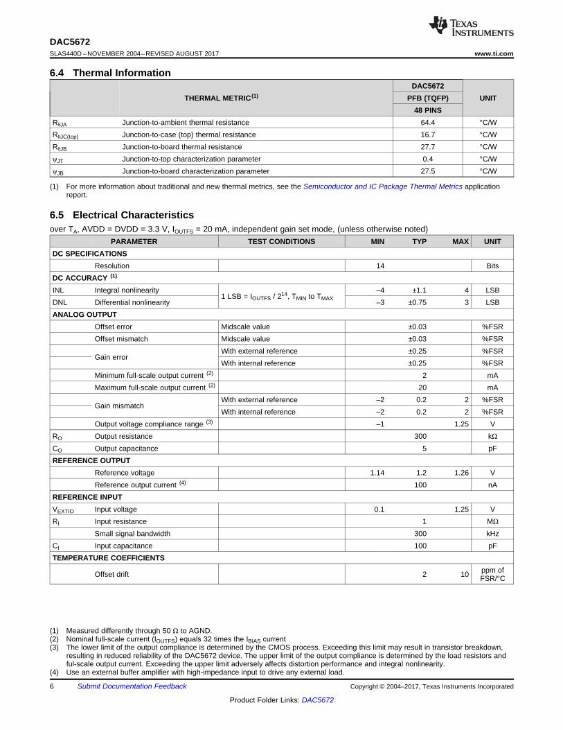
(1) For more information about traditional and new thermal metrics, see the Semiconductor and IC Package Thermal Metrics applicationreport.
6.4 Thermal Information
THERMAL METRIC (1)DAC5672
UNITPFB (TQFP)48 PINS
RθJA Junction-to-ambient thermal resistance 64.4 °C/WRθJC(top) Junction-to-case (top) thermal resistance 16.7 °C/WRθJB Junction-to-board thermal resistance 27.7 °C/WψJT Junction-to-top characterization parameter 0.4 °C/WψJB Junction-to-board characterization parameter 27.5 °C/W
(1) Measured differently through 50 Ω to AGND.(2) Nominal full-scale current (IOUTFS) equals 32 times the IBIAS current(3) The lower limit of the output compliance is determined by the CMOS process. Exceeding this limit may result in transistor breakdown,
resulting in reduced reliability of the DAC5672 device. The upper limit of the output compliance is determined by the load resistors andful-scale output current. Exceeding the upper limit adversely affects distortion performance and integral nonlinearity.
(4) Use an external buffer amplifier with high-impedance input to drive any external load.
6.5 Electrical Characteristicsover TA, AVDD = DVDD = 3.3 V, IOUTFS = 20 mA, independent gain set mode, (unless otherwise noted)
PARAMETER TEST CONDITIONS MIN TYP MAX UNITDC SPECIFICATIONS
Resolution 14 BitsDC ACCURACY (1)
INL Integral nonlinearity1 LSB = IOUTFS / 214, TMIN to TMAX
–4 ±1.1 4 LSBDNL Differential nonlinearity –3 ±0.75 3 LSBANALOG OUTPUT
Offset error Midscale value ±0.03 %FSROffset mismatch Midscale value ±0.03 %FSR
Gain errorWith external reference ±0.25 %FSRWith internal reference ±0.25 %FSR
Minimum full-scale output current (2) 2 mAMaximum full-scale output current (2) 20 mA
Gain mismatchWith external reference –2 0.2 2 %FSRWith internal reference –2 0.2 2 %FSR
Output voltage compliance range (3) –1 1.25 VRO Output resistance 300 kΩCO Output capacitance 5 pFREFERENCE OUTPUT
Reference voltage 1.14 1.2 1.26 VReference output current (4) 100 nA
REFERENCE INPUTVEXTIO Input voltage 0.1 1.25 VRI Input resistance 1 MΩ
Small signal bandwidth 300 kHzCI Input capacitance 100 pFTEMPERATURE COEFFICIENTS
Offset drift 2 10 ppm ofFSR/°C

7
DAC5672www.ti.com SLAS440D –NOVEMBER 2004–REVISED AUGUST 2017
Product Folder Links: DAC5672
Submit Documentation FeedbackCopyright © 2004–2017, Texas Instruments Incorporated
Electrical Characteristics (continued)over TA, AVDD = DVDD = 3.3 V, IOUTFS = 20 mA, independent gain set mode, (unless otherwise noted)
PARAMETER TEST CONDITIONS MIN TYP MAX UNIT
Gain drift
With external reference (DACA) 10 43 ppm ofFSR/°CWith external reference (DACB) 20 80
With internal reference 40 160 ppm ofFSR/°C
Reference voltage drift 20 ppm /°C
6.6 Electrical Characteristicsover TA, AVDD = DVDD = 3.3 V, IOUTFS = 20 mA, fDATA = 200 MSPS, fOUT = 1 MHz, independent gain set mode, (unlessotherwise noted)
PARAMETER TEST CONDITIONS MIN TYP MAX UNITPOWER SUPPLYAVDD Analog supply voltage 3 3.3 3.6 VDVDD Digital supply voltage 3 3.3 3.6 V
IAVDD Analog supply current
Including output current through loadresistor 75 90 mA
Sleep mode with clock 2.5 6 mASleep mode without clock 2.5 mA
IDVDD Digital supply currentfDATA = 200 MSPS, fOUT = 1 MHz 25 38 mASleep mode with clock 13.4 18 mASleep mode without clock 0.6 mA
Power dissipation
fDATA = 200 MSPS, fOUT = 1 MHz 330 390
mWSleep mode with clock 53Sleep mode without clock 9.2fDATA = 275 MSPS, fOUT = 20 MHz 350
APSRR Analog power supply rejection ratio –0.2 –0.01 0.2 %FSR/VDPSRR Digital power supply rejection ratio –0.2 0 0.2 %FSR/VTA Operating free-air temperature –40 85 °C
(1)
6.7 Electrical Characteristics: AC CharacteristicsAC specifications over TA , AVDD = DVDD = 3.3 V, IOUTFS = 20 mA, differential 1:1 impedance ratio transformer coupledoutput, 50-Ω doubly terminated load (unless otherwise noted)
PARAMETER TEST CONDITIONS MIN TYP MAX UNITANALOG OUTPUTfclk Maximum output update rate (1) 275 MSPSts Output settling time to 0.1% (DAC) Midscale transition 20 ns
trOutput rise time 10% to 90%(OUT) 1.4 ns
tf Output fall time 10% to 90% (OUT) 1.5 ns
Output noiseIOUTFS = 20 mA 55 pA/√HzIOUTFS = 2 mA 30 pA/√Hz
AC LINEARITY

8
DAC5672SLAS440D –NOVEMBER 2004–REVISED AUGUST 2017 www.ti.com
Product Folder Links: DAC5672
Submit Documentation Feedback Copyright © 2004–2017, Texas Instruments Incorporated
Electrical Characteristics: AC Characteristics (continued)AC specifications over TA , AVDD = DVDD = 3.3 V, IOUTFS = 20 mA, differential 1:1 impedance ratio transformer coupledoutput, 50-Ω doubly terminated load (unless otherwise noted)
PARAMETER TEST CONDITIONS MIN TYP MAX UNIT
SFDR Spurious-free dynamic range
1st Nyquist zone:TA = 25°CfDATA = 50 MSPSfOUT = 1 MHzIOUTFS = 0 dB
83
dBc
1st Nyquist zone:TA = 25°C fDATA = 50 MSPSfOUT = 1 MHzIOUTFS = –6 dB
80
1st Nyquist zone:TA = 25°CfDATA = 50 MSPSfOUT = 1 MHzIOUTFS = –12 dB
79
1st Nyquist zone:TA = 25°CfDATA = 100 MSPSfOUT = 5 MHz
84
1st Nyquist zone, TA = 25°C, fDATA = 100MSPS, fOUT = 20 MHz 79
1st Nyquist zone, TMIN to TMAX, fDATA =200 MSPS, fOUT = 20 MHz 68 75
1st Nyquist zone, TA = 25°C, fDATA = 200MSPS, fOUT = 41 MHz 72
1st Nyquist zone, TA = 25°C, fDATA = 275MSPS, fOUT = 20 MHz 74
SNR Signal-to-noise ratio
1st Nyquist zone, TA = 25°C, fDATA = 100MSPS, fOUT = 5 MHz 77 dB
1st Nyquist zone, TA = 25°C, fDATA = 160MSPS, fOUT = 20 MHz 70 dB
ACLR Adjacent channel leakage ratio
W-CDMA signal with 3.84-MHzbandwidth, fDATA = 61.44 MSPS, IF =15.360 MHz
75dB
W-CDMA signal with 3.84-MHzbandwidth, fDATA = 122.88 MSPS, IF =30.72 MHz
73 dB
W-CDMA signal with 3.84-MHzbandwidth, fDATA = 61.44 MSPS,baseband
78 dB
W-CDMA signal with 3.84-MHzbandwidth, fDATA = 122.88 MSPS,baseband
78 dB
IMD3 Third-order two-toneintermodulation
Each tone at –6 dBFS, TA = 25°C, fDATA =200 MSPS, fOUT = 45.4 MHz and 46.4MHz
65 dBc
Each tone at –6 dBFS, TA = 25°C, fDATA =100 MSPS, fOUT = 15.1 MHz and 16.1MHz
79 dBc
IMD Four-tone intermodulation
Each tone at –12 dBFS, TA = 25°C, fDATA= 100 MSPS, fOUT = 15.6, 15.8, 16.2, and16.4 MHz
79 dBc
Each tone at –12 dBFS, TA = 25°C, fDATA= 165 MSPS, fOUT = 68.8, 69.6, 71.2, and72 MHz
61 dBc
Each tone at –12 dBFS, TA = 25°C, fDATA= 165 MSPS, fOUT = 19, 19.1, 19.3, and19.4 MHz
73 dBc
−1.0−0.8−0.6−0.4−0.20.00.20.40.60.81.0
0 2000 4000 6000 8000 10000 12000 14000 16000
Input Code
DN
L −
Diff
eren
tial N
onlin
earit
y E
rror
− L
SB
G002
−1.5
−1.0
−0.5
0.0
0.5
1.0
1.5
0 2000 4000 6000 8000 10000 12000 14000 16000
Input Code
INL
− In
tegr
al N
onlin
earit
y E
rror
− L
SB
G001
9
DAC5672www.ti.com SLAS440D –NOVEMBER 2004–REVISED AUGUST 2017
Product Folder Links: DAC5672
Submit Documentation FeedbackCopyright © 2004–2017, Texas Instruments Incorporated
Electrical Characteristics: AC Characteristics (continued)AC specifications over TA , AVDD = DVDD = 3.3 V, IOUTFS = 20 mA, differential 1:1 impedance ratio transformer coupledoutput, 50-Ω doubly terminated load (unless otherwise noted)
PARAMETER TEST CONDITIONS MIN TYP MAX UNIT
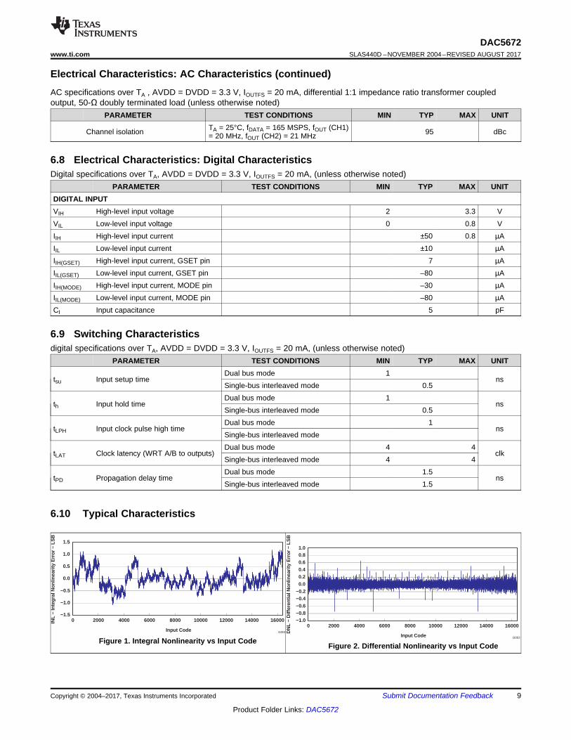
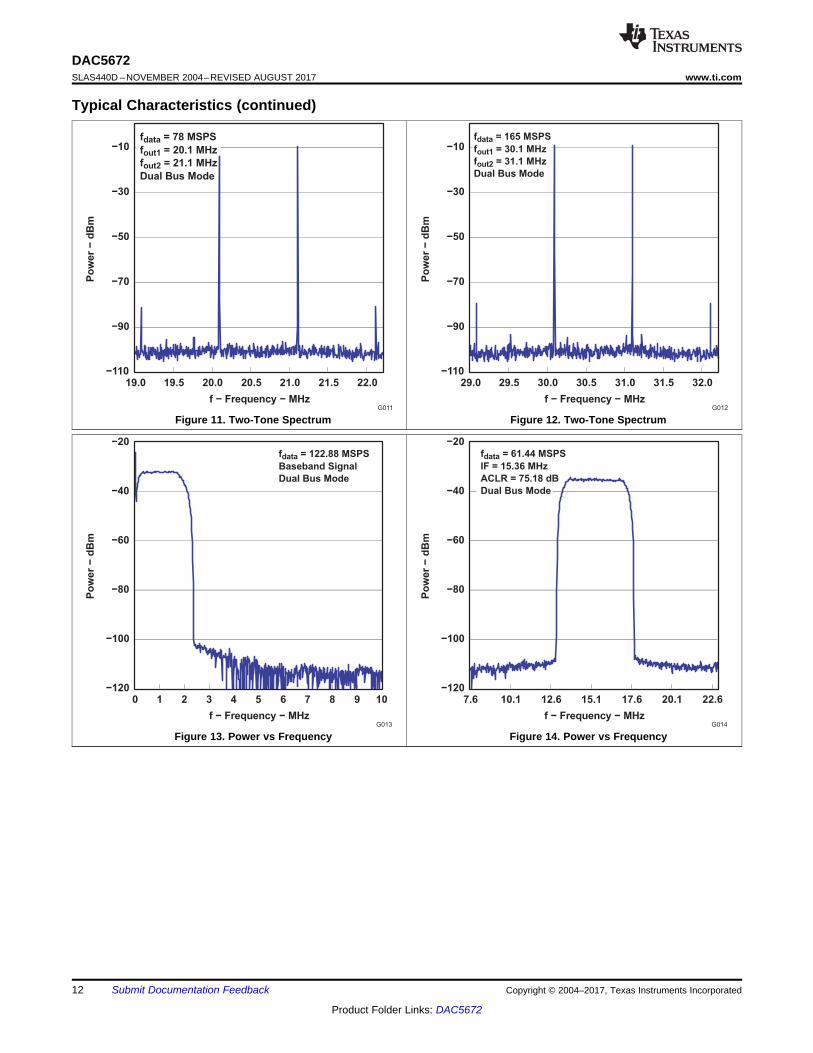
Channel isolation TA = 25°C, fDATA = 165 MSPS, fOUT (CH1)= 20 MHz, fOUT (CH2) = 21 MHz 95 dBc
6.8 Electrical Characteristics: Digital CharacteristicsDigital specifications over TA, AVDD = DVDD = 3.3 V, IOUTFS = 20 mA, (unless otherwise noted)
PARAMETER TEST CONDITIONS MIN TYP MAX UNITDIGITAL INPUTVIH High-level input voltage 2 3.3 VVIL Low-level input voltage 0 0.8 VIIH High-level input current ±50 0.8 µAIIL Low-level input current ±10 µAIIH(GSET) High-level input current, GSET pin 7 µAIIL(GSET) Low-level input current, GSET pin –80 µAIIH(MODE) High-level input current, MODE pin –30 µAIIL(MODE) Low-level input current, MODE pin –80 µACI Input capacitance 5 pF
6.9 Switching Characteristicsdigital specifications over TA, AVDD = DVDD = 3.3 V, IOUTFS = 20 mA, (unless otherwise noted)
PARAMETER TEST CONDITIONS MIN TYP MAX UNIT
tsu Input setup timeDual bus mode 1
nsSingle-bus interleaved mode 0.5
th Input hold timeDual bus mode 1
nsSingle-bus interleaved mode 0.5
tLPH Input clock pulse high timeDual bus mode 1
nsSingle-bus interleaved mode
tLAT Clock latency (WRT A/B to outputs)Dual bus mode 4 4
clkSingle-bus interleaved mode 4 4
tPD Propagation delay timeDual bus mode 1.5
nsSingle-bus interleaved mode 1.5
6.10 Typical Characteristics
Figure 1. Integral Nonlinearity vs Input Code Figure 2. Differential Nonlinearity vs Input Code

60
65
70
75
80
85
90
95
100
0 5 10 15 20 25 30 35
fout − Output Frequency − MHz
fdata = 100 MSPS
Dual Bus ModeSF
DR
−S
pu
rio
us-F
ree
Dyn
am
icR
an
ge
−d
Bc
−12 dBfS
0 dBfS
−6 dBfS
G005
60
65
70
75
80
85
90
95
100
0 5 10 15 20 25 30 35 40 45 50 55 60
fout − Output Frequency − MHz
fdata = 165 MSPS
Dual Bus ModeSF
DR
−S
pu
rio
us-F
ree
Dyn
am
icR
an
ge
−d
Bc
−12 dBfS
0 dBfS
−6 dBfS
G006
60
65
70
75
80
85
90
95
100
0 4 8 12 16 20
fout − Output Frequency − MHz
fdata = 52 MSPSDual Bus ModeS
FD
R −
Spu
rious
-Fre
e D
ynam
ic R
ange
− d
Bc
0 dBf S
−12 dBf S
−6 dBf S
G003
60
65
70
75
80
85
90
95
100
0 5 10 15 20 25 30
fout − Output Frequency − MHz
fdata = 78 MSPS
Dual Bus ModeSF
DR
−S
pu
rio
us-F
ree
Dyn
am
icR
an
ge
−d
Bc
−12 dBfS
0 dBfS
−6 dBfS
G004
10
DAC5672SLAS440D –NOVEMBER 2004–REVISED AUGUST 2017 www.ti.com
Product Folder Links: DAC5672
Submit Documentation Feedback Copyright © 2004–2017, Texas Instruments Incorporated
Typical Characteristics (continued)
Figure 3. Spurious-Free Dynamic Range vs OutputFrequency
Figure 4. Spurious-Free Dynamic Range vs OutputFrequency
Figure 5. Spurious-Free Dynamic Range vs OutputFrequency
Figure 6. Spurious-Free Dynamic Range vs OutputFrequency

fout1 − Output Frequency − MHz
60
65
70
75
80
85
90
95
0 5 10 15 20 25 30 35
Two-
Ton
e IM
D3
− dB
c
fdata = 78 MSPSDual Bus Modefout2 = fout1 + 1 MHz
G009fout1 − Output Frequency − MHz
50
55
60
65
70
75
80
85
90
95
100
0 10 20 30 40 50
Tw
o-T
on
e IM
D3
−d
Bc
fdata = 165 MSPS
Dual Bus Mode
fout2 = fout1 + 1 MHz
G010
f − Frequency − MHz
−100
−80
−60
−40
−20
0
0.0 7.8 15.6 23.4 31.2 39.0
fdata = 78 MSPSfOUT = 15 MHzDual Bus Mode
Pow
er −
dB
m
G007f − Frequency − MHz
−100
−80
−60
−40
−20
0
0.0 16.5 33.0 49.5 66.0 82.5
fdata = 165 MSPS
fOUT = 30.1 MHz
Dual Bus Mode
Po
wer
−d
Bm
G008
11
DAC5672www.ti.com SLAS440D –NOVEMBER 2004–REVISED AUGUST 2017
Product Folder Links: DAC5672
Submit Documentation FeedbackCopyright © 2004–2017, Texas Instruments Incorporated
Typical Characteristics (continued)
Figure 7. Single-Tone Spectrum Figure 8. Single-Toned Spectrum
Figure 9. Two-Tone IMD3 vs Output Frequency Figure 10. Two-Tone IMD3 vs Output Frequency
f − Frequency − MHz
−120
−100
−80
−60
−40
−20
0 1 2 3 4 5 6 7 8 9 10
fdata = 122.88 MSPS
Baseband Signal
Dual Bus Mode
Po
wer
−d
Bm
G013
f − Frequency − MHz
Po
wer
−d
Bm
−120
−100
−80
−60
−40
−20
7.6 10.1 12.6 15.1 17.6 20.1 22.6
fdata = 61.44 MSPS
IF = 15.36 MHz
ACLR = 75.18 dB
Dual Bus Mode
G014
f − Frequency − MHz
−110
−90
−70
−50
−30
−10
19.0 19.5 20.0 20.5 21.0 21.5 22.0
Po
wer
−d
Bm
fdata = 78 MSPS
fout1 = 20.1 MHz
fout2 = 21.1 MHz
Dual Bus Mode
G011
f − Frequency − MHz
−110
−90
−70
−50
−30
−10
29.0 29.5 30.0 30.5 31.0 31.5 32.0
Po
wer
−d
Bm
fdata = 165 MSPS
fout1 = 30.1 MHz
fout2 = 31.1 MHz
Dual Bus Mode
G012
12
DAC5672SLAS440D –NOVEMBER 2004–REVISED AUGUST 2017 www.ti.com
Product Folder Links: DAC5672
Submit Documentation Feedback Copyright © 2004–2017, Texas Instruments Incorporated
Typical Characteristics (continued)
Figure 11. Two-Tone Spectrum Figure 12. Two-Tone Spectrum
Figure 13. Power vs Frequency Figure 14. Power vs Frequency
f − Frequency − MHz
Pow
er −
dB
m
−120
−100
−80
−60
−40
−20
7.6 10.1 12.6 15.1 17.6 20.1 22.6
fdata = 122.88 MSPSIF = 15.36 MHzACLR = 77.16 dBDual Bus Mode
G015f − Frequency − MHz
Pow
er −
dB
m
−120
−100
−80
−60
−40
−20
23.0 25.5 28.0 30.5 33.0 35.5 38.0
fdata = 122.88 MSPSIF = 30.72 MHzACLR = 72.7 dBDual Bus Mode
G016
13
DAC5672www.ti.com SLAS440D –NOVEMBER 2004–REVISED AUGUST 2017
Product Folder Links: DAC5672
Submit Documentation FeedbackCopyright © 2004–2017, Texas Instruments Incorporated
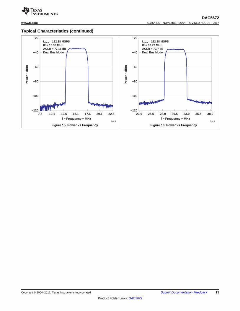
Typical Characteristics (continued)
Figure 15. Power vs Frequency Figure 16. Power vs Frequency

DE-MUX
DA[13:0]
DB[13:0]
MODE
GSET
Latch A
Latch B 14−b DAC
14−b DACIOUTA1
IOUTA2
IOUTB1
IOUTB2
1.2 V Reference
WRTB WRTA CLKB CLKA
BIASJ_A
BIASJ_B
EXTIO
DVDD DGND AVDD AGND
SLEEP
14
DAC5672SLAS440D –NOVEMBER 2004–REVISED AUGUST 2017 www.ti.com
Product Folder Links: DAC5672
Submit Documentation Feedback Copyright © 2004–2017, Texas Instruments Incorporated
7 Detailed Description
7.1 OverviewThe architecture of the DAC5672 uses a current steering technique to enable fast switching and high updaterate. The core element within the monolithic DAC is an array of segmented current sources that are designed todeliver a full-scale output current of up to 20 mA. An internal decoder addresses the differential current switcheseach time the DAC is updated and a corresponding output current is formed by steering all currents to eitheroutput summing node, IOUT1 or IOUT2. The complementary outputs deliver a differential output signal, whichimproves the dynamic performance through reduction of even-order harmonics, common-mode signals (noise),and double the peak-to-peak output signal swing by a factor of two, as compared to single-ended operation.
The segmented architecture results in a significant reduction of the glitch energy and improves the dynamicperformance (SFDR) and DNL. The current outputs maintain a very high output impedance of greaterthan 300 kΩ.
When pin 42 (GSET) is high (simultaneous gain set mode), the full-scale output current for DACs is determinedby the ratio of the internal reference voltage (1.2 V) and an external resistor (RSET) connected to BIASJ_A. WhenGSET is low (independent gain set mode), the full-scale output current for each DAC is determined by the ratioof the internal reference voltage (1.2 V) and separate external resistors (RSET) connected to BIASJ_A andBIASJ_B. The resulting IREF is internally multiplied by a factor of 32 to produce an effective DAC output currentthat can range from 2 mA to 20 mA, depending on the value of RSET.
The DAC5672 is split into a digital and an analog portion, each of which is powered through its own supply pin.The digital section includes edge-triggered input latches and the decoder logic, while the analog sectioncomprises both the current source array with its associated switches, and the reference circuitry.
7.2 Functional Block Diagram

Valid DataDA[13:0]/DB[13:0]
tsu th
tlat
tpd
tsettle
WRTA/WRTB
CLKA/CLKB
IOUTor
IOUT
t1ph
15
DAC5672www.ti.com SLAS440D –NOVEMBER 2004–REVISED AUGUST 2017
Product Folder Links: DAC5672
Submit Documentation FeedbackCopyright © 2004–2017, Texas Instruments Incorporated
7.3 Feature Description
7.3.1 Input InterfacesThe DAC5672 features two operating modes selected by the MODE pin, as shown in Table 1.• For dual-bus input mode, the device essentially consists of two separate DACs. Each DAC has its own
separate data input bus, clock input, and data write signal (data latch-in).• In single-bus interleaved mode, the data must be presented interleaved at the A-channel input bus. The B-
channel input bus is not used in this mode. The clock and write input are now shared by both DACs.
Table 1. Operating ModesMODE PIN BUS INPUT
MODE pin connected to DGND Single-bus interleaved mode, clock and write input equal for both DACsMODE pin connected to DVDD Dual-bus mode, DACs operate independently
7.3.2 Dual-Bus Data Interface and TimingIn dual-bus mode, the MODE pin is connected to DVDD. The two converter channels within the DAC5672 consistof two independent, 14-bit, parallel data ports. Each DAC channel is controlled by its own set of write (WRTA,WRTB) and clock (CLKA, CLKB) lines. The WRTA, WRTB lines control the channel input latches and the CLKA,CLKB lines control the DAC latches. The data is first loaded into the input latch by a rising edge of the WRTA,WRTB line.
The internal data transfer requires a correct sequence of write and clock inputs, since essentially two clockdomains having equal periods (but possibly different phases) are input to the DAC5672. The DAC5672 is definedby a minimum requirement of the time between the rising edge of the clock and the rising edge of the writeinputs. The rising edge of CLKA, CLKB must occur at the same time or before the rising edge of the WRTA,WRTB signal. A minimum delay of 2 ns must be maintained if the rising edge of the clock occurs after the risingedge of the write. Note that these conditions are satisfied when the clock and write inputs are connectedexternally. Note that all specifications were measured with the WRTA, WRTB and CLKA, CLKB lines connectedtogether.
Figure 17. Dual-Bus Mode Operation

16383 - CodeI = I xOUT2 OUTFS 16384
æ ö÷ç ÷ç ÷çè ø
IOUT1 IOUTFS Code16384
IOUTFS IOUT1 IOUT2
Valid DataDA[13:0]
tsu th
tlat
tpd
tsettle
SELECTIQ
WRTIQ
CLKIQ
RESETIQ
IOUTor
IOUT
16
DAC5672SLAS440D –NOVEMBER 2004–REVISED AUGUST 2017 www.ti.com
Product Folder Links: DAC5672
Submit Documentation Feedback Copyright © 2004–2017, Texas Instruments Incorporated
7.3.3 Single-Bus Interleaved Data Interface and TimingIn single-bus interleaved mode, the MODE pin is connected to DGND. Figure 18 shows the timing diagram. Ininterleaved mode, the A- and B-channels share the write input (WRTIQ) and update clock (CLKIQ and internalCLKDACIQ). Multiplexing logic directs the input word at the A-channel input bus to either the A-channel inputlatch (SELECTIQ is high) or to the B-channel input latch (SELECTIQ is low). When SELECTIQ is high, the datavalue in the B-channel latch is retained by presenting the latch output data to its input again. When SELECTIQ islow, the data value in the A-channel latch is retained by presenting the latch output data to its input.
In interleaved mode, the A-channel input data rate is twice the update rate of the DAC core. As in dual-busmode, it is important to maintain a correct sequence of write and clock inputs. The edge-triggered flip-flops latchthe A- and B-channel input words on the rising edge of the write input (WRTIQ). This data is presented to the A-and B-DAC latches on the following falling edge of the write inputs. The DAC5672 clock input is divided by afactor of two before it is presented to the DAC latches.
Correct pairing of the A- and B-channel data is done by RESETIQ. In interleaved mode, the clock input CLKIQ isdivided by two, which would translate to a non-deterministic relation between the rising edges of the CLKIQ andCLKDACIQ. RESETIQ ensures, however, that the correct position of the rising edge of CLKDACIQ with respectto the data at the input of the DAC latch is determined. CLKDACIQ is disabled (low) when RESETIQ is high.
Figure 18. Single-Bus Interleaved Mode Operation
7.4 Device Functional Modes
7.4.1 DAC Transfer FunctionEach of the DACs in the DAC5672 has a set of complementary current outputs, IOUT1 and IOUT2. The full-scaleoutput current, IOUTFS, is the summation of the two complementary output currents:
(1)
The individual output currents depend on the DAC code and can be expressed as:
(2)
(3)

AVDD
Current Source ArrayIOUT1 IOUT2
S(1) S(1)C
RLOAD RLOAD
S(2) S(2)C S(N) S(N)C
VOUTDIFF(2 Code 16383)
16384 IOUTFS RLOAD
VOUTDIFF VOUT1 VOUT2
VOUT2 IOUT2 RLOAD
VOUT1 IOUT1 RLOAD
IOUTFS 32 IREF 32VREFRSET
17
DAC5672www.ti.com SLAS440D –NOVEMBER 2004–REVISED AUGUST 2017
Product Folder Links: DAC5672
Submit Documentation FeedbackCopyright © 2004–2017, Texas Instruments Incorporated
Device Functional Modes (continued)where Code is the decimal representation of the DAC data input word. Additionally, IOUTFS is a function of thereference current IREF, which is determined by the reference voltage and the external setting resistor (RSET).
(4)
In most cases, the complementary outputs drive resistive loads or a terminated transformer. A signal voltagedevelops at each output according to:
(5)
(6)
The value of the load resistance is limited by the output compliance specification of the DAC5672. To maintainspecified linearity performance, the voltage for IOUT1 and IOUT2 must not exceed the maximum allowablecompliance range.
The total differential output voltage is:
(7)
(8)
7.4.2 Analog OutputsThe DAC5672 provides two complementary current outputs, IOUT1 and IOUT2. The simplified circuit of theanalog output stage representing the differential topology is shown in Figure 19. The output impedance of IOUT1and IOUT2 results from the parallel combination of the differential switches, along with the current sources andassociated parasitic capacitances.
Figure 19. Analog Outputs
The signal voltage swing that may develop at the two outputs, IOUT1 and IOUT2, is limited by a negative andpositive compliance. The negative limit of –1 V is given by the breakdown voltage of the CMOS process andexceeding it compromises the reliability of the DAC5672 (or even causes permanent damage). With the full-scaleoutput set to 20 mA, the positive compliance equals 1.2 V. Note that the compliance range decreases to about 1V for a selected output current of IOUTFS = 2 mA. Care must be taken that the configuration of DAC5672 does notexceed the compliance range to avoid degradation of the distortion performance and integral linearity.

IOUT11:1
IOUT2
50 Ω
50 Ω
RLOAD50 Ω100 Ω AGND
18
DAC5672SLAS440D –NOVEMBER 2004–REVISED AUGUST 2017 www.ti.com
Product Folder Links: DAC5672
Submit Documentation Feedback Copyright © 2004–2017, Texas Instruments Incorporated
Device Functional Modes (continued)Best distortion performance is typically achieved with the maximum full-scale output signal limited toapproximately 0.5 VPP. This is the case for a 50-Ω doubly-terminated load and a 20-mA full-scale output current.A variety of loads can be adapted to the output of the DAC5672 by selecting a suitable transformer whilemaintaining optimum voltage levels at IOUT1 and IOUT2. Furthermore, using the differential output configurationin combination with a transformer is instrumental for achieving excellent distortion performance. Common-modeerrors, such as even-order harmonics or noise, can be substantially reduced. This is particularly the case withhigh output frequencies.
For those applications requiring the optimum distortion and noise performance, it is recommended to select a full-scale output of 20 mA. A lower full-scale range of 2 mA may be considered for applications that require lowpower consumption, but can tolerate a slight reduction in performance level.
7.4.3 Output ConfigurationsThe current outputs of the DAC5672 allow for a variety of configurations. As mentioned previously, utilizing theconverter’s differential outputs yield the best dynamic performance. Such a differential output circuit may consistof an RF transformer or a differential amplifier configuration. The transformer configuration is ideal for mostapplications with ac coupling, while op amps are suitable for a dc-coupled configuration.
The single-ended configuration may be considered for applications requiring a unipolar output voltage.Connecting a resistor from either one of the outputs to ground converts the output current into a ground-referenced voltage signal. To improve on the dc linearity by maintaining a virtual ground, an I-to-V or op-ampconfiguration may be considered.
7.4.4 Differential With TransformerUsing an RF transformer provides a convenient way of converting the differential output signal into a single-ended signal while achieving excellent dynamic performance. The appropriate transformer must be carefullyselected based on the output frequency spectrum and impedance requirements.
The differential transformer configuration has the benefit of significantly reducing common-mode signals, thusimproving the dynamic performance over a wide range of frequencies. Furthermore, by selecting a suitableimpedance ratio (winding ratio) the transformer can provide optimum impedance matching while controlling thecompliance voltage for the converter outputs.
Figure 20 and Figure 21 show 50-Ω doubly-terminated transformer configurations with 1:1 and 4:1 impedanceratios, respectively. Note that the center tap of the primary input of the transformer has to be grounded to enablea dc-current flow. Applying a 20-mA full-scale output current would lead to a 0.5-VPP output for a 1:1 transformerand a 1-VPP output for a 4:1 transformer. In general, the 1:1 transformer configuration will have slightly betteroutput distortion, but the 4:1 transformer will have 6 dB higher output power.
Figure 20. Driving a Doubly-Terminated 50-Ω Cable Using a 1:1 Impedance Ratio Transformer

REFOUTFS REF
SET
VI 32 I 32
R u u
IOUT1
IOUT2
50 Ω25 Ω
RLOAD50 Ω
AGND
IOUT14:1
IOUT2
100 Ω
100 Ω
RLOAD50 Ω
AGND
19
DAC5672www.ti.com SLAS440D –NOVEMBER 2004–REVISED AUGUST 2017
Product Folder Links: DAC5672
Submit Documentation FeedbackCopyright © 2004–2017, Texas Instruments Incorporated
Device Functional Modes (continued)
Figure 21. Driving a Doubly-Terminated 50-Ω Cable Using a 4:1 Impedance Ratio Transformer
7.4.5 Single-Ended ConfigurationFigure 22 shows the single-ended output configuration, where the output current IOUT1 flows into an equivalentload resistance of 25 Ω. Node IOUT2 must be connected to AGND or terminated with a resistor of 25 Ω toAGND. The nominal resistor load of 25 Ω gives a differential output swing of 1 VPP when applying a 20-mA full-scale output current.
Figure 22. Driving a Doubly-Terminated 50-Ω Cable Using a Single-Ended Output
7.4.6 Reference Operation
7.4.6.1 Internal ReferenceThe DAC5672 has an on-chip reference circuit which comprises a 1.2-V bandgap reference and two controlamplifiers, one for each DAC. The full-scale output current, IOUTFS, of the DAC5672 is determined by thereference voltage, VREF, and the value of resistor RSET. IOUTFS can be calculated by:
(9)
The reference control amplifier operates as a V-to-I converter producing a reference current, IREF, which isdetermined by the ratio of VREF and RSET (see Equation 9). The full-scale output current, IOUTFS, results frommultiplying IREF by a fixed factor of 32.
Using the internal reference, a 2-kΩ resistor value results in a full-scale output of approximately 20 mA. Resistorswith a tolerance of 1% or better should be considered. Selecting higher values, the output current can beadjusted from 20 mA down to 2 mA. Operating the DAC5672 at lower than 20-mA output currents may bedesirable for reasons of reducing the total power consumption, improving the distortion performance, orobserving the output compliance voltage limitations for a given load condition.

20
DAC5672SLAS440D –NOVEMBER 2004–REVISED AUGUST 2017 www.ti.com
Product Folder Links: DAC5672
Submit Documentation Feedback Copyright © 2004–2017, Texas Instruments Incorporated
Device Functional Modes (continued)It is recommended to bypass the EXTIO pin with a ceramic chip capacitor of 0.1 μF or more. The controlamplifier is internally compensated and its small signal bandwidth is approximately 300 kHz.
7.4.6.2 External ReferenceThe internal reference can be disabled by simply applying an external reference voltage into the EXTIO pin,which in this case functions as an input. The use of an external reference may be considered for applications thatrequire higher accuracy and drift performance or to add the ability of dynamic gain control.
While a 0.1-μF capacitor is recommended to be used with the internal reference, it is optional for the externalreference operation. The reference input, EXTIO, has a high input impedance (1 MΩ) and can easily be driven byvarious sources. Note that the voltage range of the external reference must stay within the compliance range ofthe reference input.
7.4.6.3 Gain Setting OptionThe full-scale output current on the DAC5672 can be set two ways: either for each of the two DAC channelsindependently or for both channels simultaneously. For the independent gain set mode, the GSET pin (pin 42)must be low (that is, connected to AGND). In this mode, two external resistors are required — one RSETconnected to the BIASJ_A pin (pin 44) and the other to the BIASJ_B pin (pin 41). In this configuration, the userhas the flexibility to set and adjust the full-scale output current for each DAC independently, allowing for thecompensation of possible gain mismatches elsewhere within the transmit signal path.
Alternatively, bringing the GSET pin high (that is, connected to AVDD), the DAC5672 switches into thesimultaneous gain set mode. Now the full-scale output current of both DAC channels is determined by only oneexternal RSET resistor connected to the BIASJ_A pin. The resistor at the BIASJ_B pin may be removed; however,this is not required since this pin is not functional in this mode and the resistor has no effect on the gain equation.
7.4.6.4 Sleep ModeThe DAC5672 features a power-down function which can reduce the total supply current to approximately 3.1mA over the specified supply range if no clock is present. Applying a logic high to the SLEEP pin initiates thepower-down mode, while a logic low enables normal operation. When left unconnected, an internal activepulldown circuit enables the normal operation of the converter.
7.5 Programming
7.5.1 Digital Inputs and Timing
7.5.1.1 Digital InputsThe data input ports of the DAC5672 accept a standard positive coding with data bits DA13 and DB13 being themost significant bits (MSB). The converter outputs support a clock rate of up to 275 MSPS. The bestperformance is typically achieved with a symmetric duty cycle for write and clock; however, the duty cycle mayvary as long as the timing specifications are met. Similarly, the setup and hold times may be chosen within theirspecified limits.
All digital inputs of the DAC5672 are CMOS compatible. Figure 23 and Figure 24 show schematics of theequivalent CMOS digital inputs of the DAC5672. The pullup and pulldown circuitry is approximately equivalent to100 kΩ. The 14-bit digital data input follows the offset positive binary coding scheme. The DAC5672 is designedto operate with a digital supply (DVDD) of 3 V to 3.6 V.

GSET
MODE
Internal
Digital In
DVDD
400W
100kW
DGND
DA[13:0]
DB[13:0]
SLEEP
CLKA/B
WRTA/B
Internal
Digital In
DVDD
400W
100kW
DGND
21
DAC5672www.ti.com SLAS440D –NOVEMBER 2004–REVISED AUGUST 2017
Product Folder Links: DAC5672
Submit Documentation FeedbackCopyright © 2004–2017, Texas Instruments Incorporated
Programming (continued)
Figure 23. CMOS/TTL Digital Equivalent Input With Internal Pulldown Resistor
Figure 24. CMOS/TTL Digital Equivalent Input With Internal Pullup Resistor

LATCH A 14-b DAC
LATCH A 14-b DAC
1.2 V Reference
DE-MUX
WRT B WRT A CLK B CLK A
DA[13:0]
DB[13:0]
EXTIO
0.1 F
50
50
Output50
100
1:1
50
50
Output50
100
1:1
22
DAC5672SLAS440D –NOVEMBER 2004–REVISED AUGUST 2017 www.ti.com
Product Folder Links: DAC5672
Submit Documentation Feedback Copyright © 2004–2017, Texas Instruments Incorporated
8 Application and Implementation
NOTEInformation in the following applications sections is not part of the TI componentspecification, and TI does not warrant its accuracy or completeness. TI’s customers areresponsible for determining suitability of components for their purposes. Customers shouldvalidate and test their design implementation to confirm system functionality.
8.1 Application Information
8.2 Typical ApplicationA typical application for the DAC5672 is as dual or single carrier transmitter. The DAC is provided with someinput digital baseband signal and it outputs an analog carrier. A typical configuration is described below.
Figure 25. Typical Application Schematic
• Clock rate = 122.88 MHz• Input data = WCDMA with IF frequency at 30.72 MHz• AVDD= DVDD = 3.3 V
8.2.1 Design RequirementsThe requirements for this design were to generate a single WCDMA signal at an intermediate frequency of 30.72MHz. The ACLR needs to be better than 72 dBc.
8.2.2 Detailed Design ProcedureThe single carrier signal with an intermediate frequency of 30.72 MHz must be created in the digital processor ata sample rate of 122.88 Msps for DAC. These 14 bit samples are placed on the 14b CMOS input port of theDAC.
f − Frequency − MHz
Pow
er −
dB
m
−120
−100
−80
−60
−40
−20
23.0 25.5 28.0 30.5 33.0 35.5 38.0
fdata = 122.88 MSPSIF = 30.72 MHzACLR = 72.7 dBDual Bus Mode
G016
23
DAC5672www.ti.com SLAS440D –NOVEMBER 2004–REVISED AUGUST 2017
Product Folder Links: DAC5672
Submit Documentation FeedbackCopyright © 2004–2017, Texas Instruments Incorporated
Typical Application (continued)A CMOS DAC clock must be generated from a clock source at 122.88 MHz. This must be provided to the CLKpin of the DAC.
The IOUTA and IOUTB differential connections must be connected to a transformer to provide a single endedoutput. A typical 1:1 impedance transformer is used on the device EVM. The DAC5672EVM provides a goodreference for this design example.
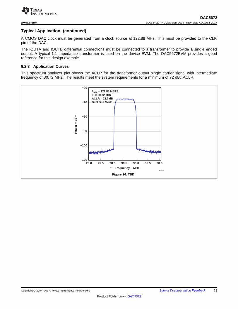
8.2.3 Application CurvesThis spectrum analyzer plot shows the ACLR for the transformer output single carrier signal with intermediatefrequency of 30.72 MHz. The results meet the system requirements for a minimum of 72 dBc ACLR.
Figure 26. TBD

24
DAC5672SLAS440D –NOVEMBER 2004–REVISED AUGUST 2017 www.ti.com
Product Folder Links: DAC5672
Submit Documentation Feedback Copyright © 2004–2017, Texas Instruments Incorporated
9 Power Supply RecommendationsIt is recommended that the device be powered with the nominal supply voltages as indicated in theRecommended Operating Conditions.
In most instances the best performance is achieved with LDO supplies. However the supplies may be driven withdirect outputs from a DC-DC switcher as long as the noise performance of the switcher is acceptable.

25
DAC5672www.ti.com SLAS440D –NOVEMBER 2004–REVISED AUGUST 2017
Product Folder Links: DAC5672
Submit Documentation FeedbackCopyright © 2004–2017, Texas Instruments Incorporated
10 Layout
10.1 Layout GuidelinesThe DAC5672 EVM layout should be used as a reference for the layout to obtain the best performance. Asample layout is shown in Figure 27 through Figure 30. Some important layout recommendations are:1. Use a single ground plane. Keep the digital and analog signals on distinct separate sections of the board.
This may be virtually divided down the middle of the device package when doing placement and layout.2. Keep the analog outputs as far away from the switching clocks and digital signals as possible. This will keep
coupling from the digital circuits to the analog outputs to a minimum.3. Decoupling caps should be kept close to the power pins of the device.
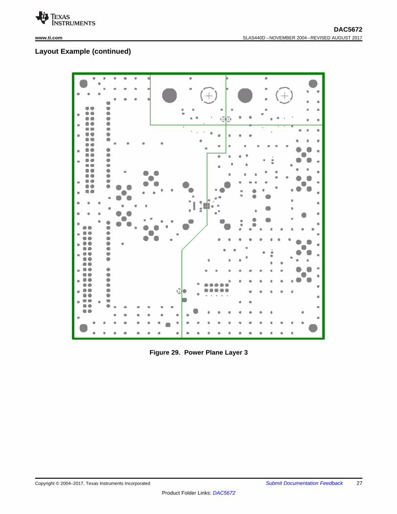
10.2 Layout ExampleThe EVM is constructed on a 4-layer, 5.1-inch x 4.8-inch, 0.062-inch thick PCB using FR−4 material. Figure 27through Figure 30 show the PCB layout for the EVM.
Figure 27. Top Layer 1

26
DAC5672SLAS440D –NOVEMBER 2004–REVISED AUGUST 2017 www.ti.com
Product Folder Links: DAC5672
Submit Documentation Feedback Copyright © 2004–2017, Texas Instruments Incorporated
Layout Example (continued)
Figure 28. Ground Plane Layer 2
27
DAC5672www.ti.com SLAS440D –NOVEMBER 2004–REVISED AUGUST 2017
Product Folder Links: DAC5672
Submit Documentation FeedbackCopyright © 2004–2017, Texas Instruments Incorporated
Layout Example (continued)
Figure 29. Power Plane Layer 3

28
DAC5672SLAS440D –NOVEMBER 2004–REVISED AUGUST 2017 www.ti.com
Product Folder Links: DAC5672
Submit Documentation Feedback Copyright © 2004–2017, Texas Instruments Incorporated
Layout Example (continued)
Figure 30. Bottom Layer 4

29
DAC5672www.ti.com SLAS440D –NOVEMBER 2004–REVISED AUGUST 2017
Product Folder Links: DAC5672
Submit Documentation FeedbackCopyright © 2004–2017, Texas Instruments Incorporated
11 Device and Documentation Support
11.1 Receiving Notification of Documentation UpdatesTo receive notification of documentation updates, navigate to the device product folder on ti.com. In the upperright corner, click on Alert me to register and receive a weekly digest of any product information that haschanged. For change details, review the revision history included in any revised document.
11.2 Community ResourcesThe following links connect to TI community resources. Linked contents are provided "AS IS" by the respectivecontributors. They do not constitute TI specifications and do not necessarily reflect TI's views; see TI's Terms ofUse.
TI E2E™ Online Community TI's Engineer-to-Engineer (E2E) Community. Created to foster collaborationamong engineers. At e2e.ti.com, you can ask questions, share knowledge, explore ideas and helpsolve problems with fellow engineers.
Design Support TI's Design Support Quickly find helpful E2E forums along with design support tools andcontact information for technical support.
11.3 TrademarksE2E is a trademark of Texas Instruments.
11.4 Electrostatic Discharge CautionThis integrated circuit can be damaged by ESD. Texas Instruments recommends that all integrated circuits be handled withappropriate precautions. Failure to observe proper handling and installation procedures can cause damage.
ESD damage can range from subtle performance degradation to complete device failure. Precision integrated circuits may be moresusceptible to damage because very small parametric changes could cause the device not to meet its published specifications.
11.5 GlossarySLYZ022 — TI Glossary.
This glossary lists and explains terms, acronyms, and definitions.
12 Mechanical, Packaging, and Orderable InformationThe following pages include mechanical, packaging, and orderable information. This information is the mostcurrent data available for the designated devices. This data is subject to change without notice and revision ofthis document. For browser-based versions of this data sheet, refer to the left-hand navigation.

PACKAGE OPTION ADDENDUM
www.ti.com 8-Jun-2017
Addendum-Page 1
PACKAGING INFORMATION
Orderable Device Status(1)
Package Type PackageDrawing
Pins PackageQty
Eco Plan(2)
Lead/Ball Finish(6)
MSL Peak Temp(3)
Op Temp (°C) Device Marking(4/5)
Samples
DAC5672IPFB ACTIVE TQFP PFB 48 250 Green (RoHS& no Sb/Br)
CU NIPDAU Level-2-260C-1 YEAR -40 to 85 DAC5672I
DAC5672IPFBR ACTIVE TQFP PFB 48 1000 Green (RoHS& no Sb/Br)
CU NIPDAU Level-2-260C-1 YEAR -40 to 85 DAC5672I
(1) The marketing status values are defined as follows:ACTIVE: Product device recommended for new designs.LIFEBUY: TI has announced that the device will be discontinued, and a lifetime-buy period is in effect.NRND: Not recommended for new designs. Device is in production to support existing customers, but TI does not recommend using this part in a new design.PREVIEW: Device has been announced but is not in production. Samples may or may not be available.OBSOLETE: TI has discontinued the production of the device.
(2) RoHS: TI defines "RoHS" to mean semiconductor products that are compliant with the current EU RoHS requirements for all 10 RoHS substances, including the requirement that RoHS substancedo not exceed 0.1% by weight in homogeneous materials. Where designed to be soldered at high temperatures, "RoHS" products are suitable for use in specified lead-free processes. TI mayreference these types of products as "Pb-Free".RoHS Exempt: TI defines "RoHS Exempt" to mean products that contain lead but are compliant with EU RoHS pursuant to a specific EU RoHS exemption.Green: TI defines "Green" to mean the content of Chlorine (Cl) and Bromine (Br) based flame retardants meet JS709B low halogen requirements of <=1000ppm threshold. Antimony trioxide basedflame retardants must also meet the <=1000ppm threshold requirement.
(3) MSL, Peak Temp. - The Moisture Sensitivity Level rating according to the JEDEC industry standard classifications, and peak solder temperature.
(4) There may be additional marking, which relates to the logo, the lot trace code information, or the environmental category on the device.
(5) Multiple Device Markings will be inside parentheses. Only one Device Marking contained in parentheses and separated by a "~" will appear on a device. If a line is indented then it is a continuationof the previous line and the two combined represent the entire Device Marking for that device.
(6) Lead/Ball Finish - Orderable Devices may have multiple material finish options. Finish options are separated by a vertical ruled line. Lead/Ball Finish values may wrap to two lines if the finishvalue exceeds the maximum column width.
Important Information and Disclaimer:The information provided on this page represents TI's knowledge and belief as of the date that it is provided. TI bases its knowledge and belief on informationprovided by third parties, and makes no representation or warranty as to the accuracy of such information. Efforts are underway to better integrate information from third parties. TI has taken andcontinues to take reasonable steps to provide representative and accurate information but may not have conducted destructive testing or chemical analysis on incoming materials and chemicals.TI and TI suppliers consider certain information to be proprietary, and thus CAS numbers and other limited information may not be available for release.
In no event shall TI's liability arising out of such information exceed the total purchase price of the TI part(s) at issue in this document sold by TI to Customer on an annual basis.

PACKAGE OPTION ADDENDUM
www.ti.com 8-Jun-2017
Addendum-Page 2
OTHER QUALIFIED VERSIONS OF DAC5672 :
• Enhanced Product: DAC5672-EP
NOTE: Qualified Version Definitions:
• Enhanced Product - Supports Defense, Aerospace and Medical Applications

TAPE AND REEL INFORMATION
*All dimensions are nominal
Device PackageType
PackageDrawing
Pins SPQ ReelDiameter
(mm)
ReelWidth
W1 (mm)
A0(mm)
B0(mm)
K0(mm)
P1(mm)
W(mm)
Pin1Quadrant
DAC5672IPFBR TQFP PFB 48 1000 330.0 16.4 9.6 9.6 1.5 12.0 16.0 Q2
PACKAGE MATERIALS INFORMATION
www.ti.com 8-Jun-2017
Pack Materials-Page 1
*All dimensions are nominal
Device Package Type Package Drawing Pins SPQ Length (mm) Width (mm) Height (mm)
DAC5672IPFBR TQFP PFB 48 1000 367.0 367.0 38.0
PACKAGE MATERIALS INFORMATION
www.ti.com 8-Jun-2017
Pack Materials-Page 2

MECHANICAL DATA
MTQF019A – JANUARY 1995 – REVISED JANUARY 1998
POST OFFICE BOX 655303 • DALLAS, TEXAS 75265
PFB (S-PQFP-G48) PLASTIC QUAD FLATPACK
4073176/B 10/96
Gage Plane
0,13 NOM
0,25
0,450,75
Seating Plane
0,05 MIN
0,170,27
24
25
13
12
SQ
36
37
7,206,80
48
1
5,50 TYP
SQ8,809,20
1,050,95
1,20 MAX0,08
0,50 M0,08
0°–7°
NOTES: A. All linear dimensions are in millimeters.B. This drawing is subject to change without notice.C. Falls within JEDEC MS-026


IMPORTANT NOTICE
Texas Instruments Incorporated (TI) reserves the right to make corrections, enhancements, improvements and other changes to itssemiconductor products and services per JESD46, latest issue, and to discontinue any product or service per JESD48, latest issue. Buyersshould obtain the latest relevant information before placing orders and should verify that such information is current and complete.TI’s published terms of sale for semiconductor products (http://www.ti.com/sc/docs/stdterms.htm) apply to the sale of packaged integratedcircuit products that TI has qualified and released to market. Additional terms may apply to the use or sale of other types of TI products andservices.Reproduction of significant portions of TI information in TI data sheets is permissible only if reproduction is without alteration and isaccompanied by all associated warranties, conditions, limitations, and notices. TI is not responsible or liable for such reproduceddocumentation. Information of third parties may be subject to additional restrictions. Resale of TI products or services with statementsdifferent from or beyond the parameters stated by TI for that product or service voids all express and any implied warranties for theassociated TI product or service and is an unfair and deceptive business practice. TI is not responsible or liable for any such statements.Buyers and others who are developing systems that incorporate TI products (collectively, “Designers”) understand and agree that Designersremain responsible for using their independent analysis, evaluation and judgment in designing their applications and that Designers havefull and exclusive responsibility to assure the safety of Designers' applications and compliance of their applications (and of all TI productsused in or for Designers’ applications) with all applicable regulations, laws and other applicable requirements. Designer represents that, withrespect to their applications, Designer has all the necessary expertise to create and implement safeguards that (1) anticipate dangerousconsequences of failures, (2) monitor failures and their consequences, and (3) lessen the likelihood of failures that might cause harm andtake appropriate actions. Designer agrees that prior to using or distributing any applications that include TI products, Designer willthoroughly test such applications and the functionality of such TI products as used in such applications.TI’s provision of technical, application or other design advice, quality characterization, reliability data or other services or information,including, but not limited to, reference designs and materials relating to evaluation modules, (collectively, “TI Resources”) are intended toassist designers who are developing applications that incorporate TI products; by downloading, accessing or using TI Resources in anyway, Designer (individually or, if Designer is acting on behalf of a company, Designer’s company) agrees to use any particular TI Resourcesolely for this purpose and subject to the terms of this Notice.TI’s provision of TI Resources does not expand or otherwise alter TI’s applicable published warranties or warranty disclaimers for TIproducts, and no additional obligations or liabilities arise from TI providing such TI Resources. TI reserves the right to make corrections,enhancements, improvements and other changes to its TI Resources. TI has not conducted any testing other than that specificallydescribed in the published documentation for a particular TI Resource.Designer is authorized to use, copy and modify any individual TI Resource only in connection with the development of applications thatinclude the TI product(s) identified in such TI Resource. NO OTHER LICENSE, EXPRESS OR IMPLIED, BY ESTOPPEL OR OTHERWISETO ANY OTHER TI INTELLECTUAL PROPERTY RIGHT, AND NO LICENSE TO ANY TECHNOLOGY OR INTELLECTUAL PROPERTYRIGHT OF TI OR ANY THIRD PARTY IS GRANTED HEREIN, including but not limited to any patent right, copyright, mask work right, orother intellectual property right relating to any combination, machine, or process in which TI products or services are used. Informationregarding or referencing third-party products or services does not constitute a license to use such products or services, or a warranty orendorsement thereof. Use of TI Resources may require a license from a third party under the patents or other intellectual property of thethird party, or a license from TI under the patents or other intellectual property of TI.TI RESOURCES ARE PROVIDED “AS IS” AND WITH ALL FAULTS. TI DISCLAIMS ALL OTHER WARRANTIES ORREPRESENTATIONS, EXPRESS OR IMPLIED, REGARDING RESOURCES OR USE THEREOF, INCLUDING BUT NOT LIMITED TOACCURACY OR COMPLETENESS, TITLE, ANY EPIDEMIC FAILURE WARRANTY AND ANY IMPLIED WARRANTIES OFMERCHANTABILITY, FITNESS FOR A PARTICULAR PURPOSE, AND NON-INFRINGEMENT OF ANY THIRD PARTY INTELLECTUALPROPERTY RIGHTS. TI SHALL NOT BE LIABLE FOR AND SHALL NOT DEFEND OR INDEMNIFY DESIGNER AGAINST ANY CLAIM,INCLUDING BUT NOT LIMITED TO ANY INFRINGEMENT CLAIM THAT RELATES TO OR IS BASED ON ANY COMBINATION OFPRODUCTS EVEN IF DESCRIBED IN TI RESOURCES OR OTHERWISE. IN NO EVENT SHALL TI BE LIABLE FOR ANY ACTUAL,DIRECT, SPECIAL, COLLATERAL, INDIRECT, PUNITIVE, INCIDENTAL, CONSEQUENTIAL OR EXEMPLARY DAMAGES INCONNECTION WITH OR ARISING OUT OF TI RESOURCES OR USE THEREOF, AND REGARDLESS OF WHETHER TI HAS BEENADVISED OF THE POSSIBILITY OF SUCH DAMAGES.Unless TI has explicitly designated an individual product as meeting the requirements of a particular industry standard (e.g., ISO/TS 16949and ISO 26262), TI is not responsible for any failure to meet such industry standard requirements.Where TI specifically promotes products as facilitating functional safety or as compliant with industry functional safety standards, suchproducts are intended to help enable customers to design and create their own applications that meet applicable functional safety standardsand requirements. Using products in an application does not by itself establish any safety features in the application. Designers mustensure compliance with safety-related requirements and standards applicable to their applications. Designer may not use any TI products inlife-critical medical equipment unless authorized officers of the parties have executed a special contract specifically governing such use.Life-critical medical equipment is medical equipment where failure of such equipment would cause serious bodily injury or death (e.g., lifesupport, pacemakers, defibrillators, heart pumps, neurostimulators, and implantables). Such equipment includes, without limitation, allmedical devices identified by the U.S. Food and Drug Administration as Class III devices and equivalent classifications outside the U.S.TI may expressly designate certain products as completing a particular qualification (e.g., Q100, Military Grade, or Enhanced Product).Designers agree that it has the necessary expertise to select the product with the appropriate qualification designation for their applicationsand that proper product selection is at Designers’ own risk. Designers are solely responsible for compliance with all legal and regulatoryrequirements in connection with such selection.Designer will fully indemnify TI and its representatives against any damages, costs, losses, and/or liabilities arising out of Designer’s non-compliance with the terms and provisions of this Notice.
Mailing Address: Texas Instruments, Post Office Box 655303, Dallas, Texas 75265Copyright © 2017, Texas Instruments Incorporated