da14580 fs - mouser.com
TRANSCRIPT

Datasheet Revision 3.4 09-Nov-2016
CFR0011-120-01 1 of 234 © 2014 Dialog Semiconductor
DA14580
Bluetooth Low Energy 4.2 SoC FINAL
General DescriptionThe DA14580 integrated circuit has a fully integratedradio transceiver and baseband processor for Blue-tooth® low energy. It can be used as a standaloneapplication processor or as a data pump in hosted sys-tems.
The DA14580 supports a flexible memory architecturefor storing Bluetooth profiles and custom applicationcode, which can be updated over the air (OTA). Thequalified Bluetooth low energy protocol stack is storedin a dedicated ROM. All software runs on the ARM®
Cortex®-M0 processor via a simple scheduler.
The Bluetooth low energy firmware includes theL2CAP service layer protocols, Security Manager(SM), Attribute Protocol (ATT), the Generic AttributeProfile (GATT) and the Generic Access Profile (GAP).All profiles published by the Bluetooth SIG as well ascustom profiles are supported.
The transceiver interfaces directly to the antenna andis fully compliant with the Bluetooth 4.2 standard.
The DA14580 has dedicated hardware for the LinkLayer implementation of Bluetooth low energy andinterface controllers for enhanced connectivity capabili-ties.
Features Complies with Bluetooth V4.2, ETSI EN 300 328 and
EN 300 440 Class 2 (Europe), FCC CFR47 Part 15 (US) and ARIB STD-T66 (Japan)
Processing power 16 MHz 32 bit ARM Cortex-M0 with SWD inter-
face Dedicated Link Layer Processor AES-128 bit encryption Processor
Memories 32 kB One-Time-Programmable (OTP) memory
42 kB System SRAM 84 kB ROM 8 kB Retention SRAM
Power management Integrated Buck/Boost DC-DC converter P0, P1, P2 and P3 ports with 3.3 V tolerance Easy decoupling of only 4 supply pins Supports coin (typ. 3.0 V) and alkaline (typ. 1.5 V)
battery cells 10-bit ADC for battery voltage measurement
Digital controlled oscillators 16 MHz crystal (±20 ppm max) and RC oscillator 32 kHz crystal (±50 ppm, ±500 ppm max) and
RCX oscillator General purpose, Capture and Sleep timers Digital interfaces General purpose I/Os: 14 (WLCSP34 package),
24 (QFN40 package), 32 (QFN48 package) 2 UARTs with hardware flow control up to 1 MBd SPI+™ interface I2C bus at 100 kHz, 400 kHz 3-axes capable Quadrature Decoder
Analog interfaces 4-channel 10-bit ADC
Radio transceiver Fully integrated 2.4 GHz CMOS transceiver Single wire antenna: no RF matching or RX/TX
switching required Supply current at VBAT3V:
TX: 3.4 mA, RX: 3.7 mA (with ideal DC-DC) 0 dBm transmit output power -20 dBm output power in “Near Field Mode” -93 dBm receiver sensitivity
Packages: WLCSP 34 pins, 2.436 mm x 2.436 mm QFN 40 pins, 5 mm x 5 mm QFN 48 pins, 6 mm x 6 mm KGD (wafer, dice)
________________________________________________________________________________________________
System Diagram

Datasheet Revision 3.4 09-Nov-2016
CFR0011-120-01 2 of 234 © 2014 Dialog Semiconductor
DA14580
Bluetooth Low Energy 4.2 SoC FINAL
ContentsGeneral Description . . . . . . . . . . . . . . . . . . . . . . . . . . . 1
Features . . . . . . . . . . . . . . . . . . . . . . . . . . . . . . . . . . . . . 1
System Diagram . . . . . . . . . . . . . . . . . . . . . . . . . . . . . . 1
Contents. . . . . . . . . . . . . . . . . . . . . . . . . . . . . . . . . . . . . 2
1 Block Diagram . . . . . . . . . . . . . . . . . . . . . . . . . . . . . . 4
2 Pinout . . . . . . . . . . . . . . . . . . . . . . . . . . . . . . . . . . . . . 5
3 Ordering Information . . . . . . . . . . . . . . . . . . . . . . . . 9
4 System Overview. . . . . . . . . . . . . . . . . . . . . . . . . . . 10
4.1 INTERNAL BLOCKS . . . . . . . . . . . . . . . . . . . . 10
4.2 FUNCTIONAL MODES . . . . . . . . . . . . . . . . . . 10
4.3 OTP MEMORY LAYOUT . . . . . . . . . . . . . . . . .11
4.3.1 OTP Header. . . . . . . . . . . . . . . . . . . . . . .11
4.4 SYSTEM START PROCEDURE . . . . . . . . . . . 12
4.4.1 Power/Wake-Up Sequence . . . . . . . . . . 13
4.4.2 OTP Mirroring . . . . . . . . . . . . . . . . . . . . 14
4.4.3 BootROM Sequence . . . . . . . . . . . . . . . 15
4.5 POWER SUPPLY CONFIGURATION . . . . . . 17
4.5.1 Power Domains . . . . . . . . . . . . . . . . . . . 17
4.5.2 Power Modes. . . . . . . . . . . . . . . . . . . . . 18
4.5.3 Retention Registers . . . . . . . . . . . . . . . . 18
5 Reset. . . . . . . . . . . . . . . . . . . . . . . . . . . . . . . . . . . . . 20
5.1 POR, HW AND SW RESET . . . . . . . . . . . . . . 20
6 ARM Cortex-M0 . . . . . . . . . . . . . . . . . . . . . . . . . . . . 21
6.1 INTERRUPTS . . . . . . . . . . . . . . . . . . . . . . . . . 22
6.2 SYSTEM TIMER (SYSTICK). . . . . . . . . . . . . . 23
6.3 WAKE-UP INTERRUPT CONTROLLER. . . . . 23
6.4 REFERENCE . . . . . . . . . . . . . . . . . . . . . . . . . 23
7 AMBA Bus Overview. . . . . . . . . . . . . . . . . . . . . . . . 24
8 Patch Block . . . . . . . . . . . . . . . . . . . . . . . . . . . . . . . 25
9 Memory Map . . . . . . . . . . . . . . . . . . . . . . . . . . . . . . 26
10 Memory Controller . . . . . . . . . . . . . . . . . . . . . . . . 28
10.1 ARBITRATION . . . . . . . . . . . . . . . . . . . . . . . 28
11 Clock Generation. . . . . . . . . . . . . . . . . . . . . . . . . . 29
11.1 CRYSTAL OSCILLATORS . . . . . . . . . . . . . . 29
11.1.1 Frequency Control (16 MHz Crystal) . . 29
11.1.2 Automated Trimming Mechanism . . . . 29
11.2 RC OSCILLATORS . . . . . . . . . . . . . . . . . . . . 30
11.2.1 Frequency Calibration . . . . . . . . . . . . . 30
11.3 SYSTEM CLOCK GENERATION . . . . . . . . . 31
11.4 GENERAL CLOCK CONSTRAINTS . . . . . . . 32
12 OTP Controller. . . . . . . . . . . . . . . . . . . . . . . . . . . . 33
12.1 OPERATING MODES . . . . . . . . . . . . . . . . . . 33
12.2 AHB MASTER INTERFACE . . . . . . . . . . . . . 33
13 I2C Interface. . . . . . . . . . . . . . . . . . . . . . . . . . . . . . 34
13.1 I2C BUS TERMS . . . . . . . . . . . . . . . . . . . . . . 34
13.1.1 Bus Transfer Terms . . . . . . . . . . . . . . . 35
13.2 I2C BEHAVIOR . . . . . . . . . . . . . . . . . . . . . . . 35
13.2.1 START and STOP Generation . . . . . . . 36
13.2.2 Combined Formats . . . . . . . . . . . . . . . 36
13.3 I2C PROTOCOLS . . . . . . . . . . . . . . . . . . . . . 36
13.3.1 START and STOP Conditions . . . . . . . 36
13.3.2 Addressing Slave Protocol. . . . . . . . . . 36
13.3.3 Transmitting and Receiving Protocols . 37
13.4 MULTIPLE MASTER ARBITRATION . . . . . . 39
13.5 CLOCK SYNCHRONIZATION . . . . . . . . . . . 40
13.6 OPERATION MODES . . . . . . . . . . . . . . . . . . 41
13.6.1 Slave Mode Operation . . . . . . . . . . . . . 41
13.6.2 Master Mode Operation . . . . . . . . . . . . 43
13.6.3 Disabling the I2C Controller . . . . . . . . . 43
14 UART . . . . . . . . . . . . . . . . . . . . . . . . . . . . . . . . . . . 44
14.1 UART (RS232) SERIAL PROTOCOL . . . . . . 45
14.2 IRDA 1.0 SIR PROTOCOL . . . . . . . . . . . . . . 45
14.3 CLOCK SUPPORT . . . . . . . . . . . . . . . . . . . . 46
14.4 INTERRUPTS . . . . . . . . . . . . . . . . . . . . . . . . 47
14.5 PROGRAMMABLE THRE INTERRUPT . . . . 47
14.6 SHADOW REGISTERS . . . . . . . . . . . . . . . . 49
14.7 DIRECT TEST MODE . . . . . . . . . . . . . . . . . . 49
15 SPI+ Interface . . . . . . . . . . . . . . . . . . . . . . . . . . . . 50
15.1 OPERATION WITHOUT FIFOS . . . . . . . . . . 50
15.2 9 BITS MODE . . . . . . . . . . . . . . . . . . . . . . . . 51
16 Quadrature Decoder . . . . . . . . . . . . . . . . . . . . . . . 54
17 Wake-Up Timer . . . . . . . . . . . . . . . . . . . . . . . . . . . 55
18 General Purpose Timers. . . . . . . . . . . . . . . . . . . . 56
18.1 TIMER 0 . . . . . . . . . . . . . . . . . . . . . . . . . . . . 56
18.2 TIMER 2 . . . . . . . . . . . . . . . . . . . . . . . . . . . . 58
19 Watchdog Timer . . . . . . . . . . . . . . . . . . . . . . . . . . 60
20 Keyboard Controller . . . . . . . . . . . . . . . . . . . . . . . 61
20.1 KEYBOARD SCANNER . . . . . . . . . . . . . . . . 61
20.2 GPIO INTERRUPT GENERATOR . . . . . . . . 61

Datasheet Revision 3.4 09-Nov-2016
CFR0011-120-01 3 of 234 © 2014 Dialog Semiconductor
DA14580
Bluetooth Low Energy 4.2 SoC FINAL
21 Input/Output Ports. . . . . . . . . . . . . . . . . . . . . . . . . 63
21.1 PROGRAMMABLE PIN ASSIGNMENT . . . . 63
21.2 GENERAL PURPOSE PORT REGISTERS . 63
21.2.1 Port Data Register . . . . . . . . . . . . . . . . 64
21.2.2 Port Set Data Output Register . . . . . . . 64
21.2.3 Port Reset Data Output Register . . . . . 64
21.3 FIXED ASSIGNMENT FUNCTIONALITY . . . 64
22 General Purpose ADC. . . . . . . . . . . . . . . . . . . . . . 65
22.1 INPUT CHANNELS AND INPUT SCALE . . . 65
22.2 STARTING THE ADC AND SAMPLING RATE
. . . . . . . . . . . . . . . . . . . . . . . . . . . . . . . . . . . 65
22.3 NON-IDEAL EFFECTS . . . . . . . . . . . . . . . . . 66
22.4 CHOPPING . . . . . . . . . . . . . . . . . . . . . . . . . . 66
22.5 OFFSET CALIBRATION . . . . . . . . . . . . . . . . 66
22.6 ZERO-SCALE ADJUSTMENT . . . . . . . . . . . 67
22.7 COMMON MODE ADJUSTMENT. . . . . . . . . 67
22.8 INPUT IMPEDANCE, INDUCTANCE AND IN-
PUT SETTLING. . . . . . . . . . . . . . . . . . . . . . . . 67
22.9 DELAY COUNTER . . . . . . . . . . . . . . . . . . . . 68
23 Power Management. . . . . . . . . . . . . . . . . . . . . . . . 69
24 BLE Core . . . . . . . . . . . . . . . . . . . . . . . . . . . . . . . . 72
24.1 EXCHANGE MEMORY . . . . . . . . . . . . . . . . . 72
24.2 PROGRAMMING BLE WAKE UP IRQ . . . . . 74
24.3 SWITCH FROM ACTIVE MODE TO DEEP
SLEEP MODE. . . . . . . . . . . . . . . . . . . . . . . . . 74
24.4 SWITCH FROM DEEP SLEEP MODE TO AC-
TIVE MODE. . . . . . . . . . . . . . . . . . . . . . . . . . . 75
24.4.1 Switching at Anchor Points . . . . . . . . . 75
24.4.2 Switching Due to an External Event . . 77
25 Radio . . . . . . . . . . . . . . . . . . . . . . . . . . . . . . . . . . . 78
25.1 RECEIVER . . . . . . . . . . . . . . . . . . . . . . . . . . 78
25.2 SYNTHESIZER . . . . . . . . . . . . . . . . . . . . . . . 78
25.3 TRANSMITTER . . . . . . . . . . . . . . . . . . . . . . . 78
25.4 RFIO . . . . . . . . . . . . . . . . . . . . . . . . . . . . . . . 78
25.5 BIASING . . . . . . . . . . . . . . . . . . . . . . . . . . . . 78
25.6 CONTROL. . . . . . . . . . . . . . . . . . . . . . . . . . . 78
26 Registers . . . . . . . . . . . . . . . . . . . . . . . . . . . . . . . . 79
27 Specifications . . . . . . . . . . . . . . . . . . . . . . . . . . . 218
28 Package Information. . . . . . . . . . . . . . . . . . . . . . 230
28.1 MOISTURE SENSITIVITY LEVEL (MSL) . . 230
28.2 WLCSP HANDLING . . . . . . . . . . . . . . . . . . 230
28.3 SOLDERING INFORMATION . . . . . . . . . . . 230
28.4 PACKAGE OUTLINES . . . . . . . . . . . . . . . . 231

Datasheet Revision 3.4 09-Nov-2016
CFR0011-120-01 4 of 234 © 2014 Dialog Semiconductor
DA14580
Bluetooth Low Energy 4.2 SoC FINAL
1 Block Diagram
Figure 1: DA14580 Block Diagram
24 April 2012
ARM Cortex M0
SWD (JTAG)
COREPOReset
BLE Core
LINK LAYER HARDWARE
AES-128Radio
TransceiverA
PB
bri
dg
e
PO
WE
R/C
LO
CK
Man
agem
en
t (P
MU
)
DCDC (BUCK/BOOST)
GPIO MULTIPLEXING
XTAL16 MHz
XTAL32.768 kHz
RC32 kHz
SW TIMER
GP
AD
C
SP
I
ROM84 kB
System/Exchange
RAM42 kB
Ret. RAM 2 kB
RC16 MHz
Me
mo
ry C
on
tro
ller
OTP32 kB
DMA
OTPC
QU
AD
D
EC
OD
ER
LDO SYS
LDO RET
LDO SYSLDO SYSLDO RF
WA
KE
UP
T
IME
R
Ret. RAM2 3 kB
Ret. RAM3 2 kB
Ret. RAM4 1 kB
KE
YB
OA
RD
C
TR
L
UA
RT
FIF
O
UA
RT
2F
IFO
I2C
FIF
O
RCX
Timer 01x PWM
Timer 23x PWM

Datasheet Revision 3.4 09-Nov-2016
CFR0011-120-01 5 of 234 © 2014 Dialog Semiconductor
DA14580
Bluetooth Low Energy 4.2 SoC FINAL
2 PinoutThe DA14580 comes in three packages:
• Wafer Level Chip Scale Package (WLCSP) with 34 balls
• Quad Flat Package No Leads (QFN) with 48 pins
• Quad Flat Package No Leads (QFN) with 40 pins
The actual pin/ball assignment is depicted in the follow-ing figures:
Figure 2: WLCSP34 ball assignment
1 2 3 4 5
A
B
C
D
E
6
F
RFIOm
RFIOp
XTAL16M
m
XTAL16M
p
SW_C
LK
SWDIO
VBAT1V
SWIT
CH
VDCDC_RF
P1_3
P1_2
P1_1
P1_0
VDCDC
GNDGND
RST
VBAT_RF
GND
VBAT3V
XTAL32K
p
XTAL32K
m
GND
P0_1
P0_2
P0_4
P0_7
VPP
P0_0
P0_3
P0_5
P0_6
GND
GND
Figure 3: QFN48 Pin Assignment
Pin 0: GND plane
RF
IOp
DA14580
(Top View)
9
8
7
6
5
4
3
2P0_1
P0_2
P0_3
P3_0
P0_4
P0_5
P0_6
11
10
P0_7
P2_1
P3_1
1
12
14
15
16
17
18
19
20
21
XT
AL3
2K
p
P2_
2
VB
AT
_RF
P3_
4
VB
AT
3V
GN
D
RS
T
P2_
32
2
23
XT
AL3
2Km
VD
CD
C
13
24
28
29
30
31
32
33
34
35 XTAL16Mm
XTAL16Mp
P1_3
P1_2
SW_CLK
SWDIO
P1_1
VBAT1V
26
27
SWITCH
P1_0
36
25
NC
VP
P
P2_
8
P2_
7
RF
IOm
P2_
6
P2_
5
47
P3
_7
P2_
9
46 45 44 43 42 41 40 39 38
P0_0
P3_2
VD
CD
C_
RF
3748P
2_0
P3_
3
P2_
4
P3_5
P3_6

Datasheet Revision 3.4 09-Nov-2016
CFR0011-120-01 6 of 234 © 2014 Dialog Semiconductor
DA14580
Bluetooth Low Energy 4.2 SoC FINAL
Figure 4: QFN40 Pin Assignment
Table 1: Pin Description
Pin Name TypeDrive(mA)
ResetState
Description
General Purpose I/Os
P0_0P0_1P0_2P0_3P0_4P0_5P0_6P0_7
DIODIODIODIODIODIODIODIO
4.8 I-PDI-PDI-PDI-PDI-PDI-PDI-PDI-PD
INPUT/OUTPUT with selectable pull up/down resistor. Pull-down enabled during and after reset. General purpose I/O port bit or alternate function nodes. Contains state retention mechanism during power down.
P1_0P1_1P1_2P1_3P1_4/SWCLKP1_5/SW_DIO
DIODIODIODIODIODIO
4.8 I-PDI-PDI-PDI-PDI-PDI-PU
INPUT/OUTPUT with selectable pull up/down resistor. Pull-down enabled during and after reset. General purpose I/O port bit or alternate function nodes. Contains state retention mechanism during power down.This signal is the JTAG clock by defaultThis signal is the JTAG data I/O by default
P2_0P2_1P2_2P2_3P2_4P2_5P2_6P2_7P2_8P2_9
DIODIODIODIODIODIODIODIODIODIO
4.8 I-PDI-PDI-PDI-PDI-PDI-PDI-PDI-PDI-PDI-PD
INPUT/OUTPUT with selectable pull up/down resistor. Pull-down enabled during and after reset. General purpose I/O port bit or alternate function nodes. Contains state retention mechanism during power down. NOTE: This port is only available on the QFN40/QFN48 pack-ages.
11 12 13 14 15 16 17 18
8
7
6
5
4
3
2
1
23
24
25
26
27
28
29
30
Pin 0: GND plane
P2_
7
P0_0
P0_1
P0_2
P0_3
NC
P0_4
P2_1
XTAL16Mm
XTAL16Mp
P1_3
P1_2
SW_CLK
SWDIO
P1_1
VBAT1VX
TA
L32K
p
P2
_2
VB
AT
_RF
VB
AT
3V
GN
D
RS
T
P2
_3
VD
CD
C
P2_
9
VP
P
P2_
8
RF
IOp
RF
IOm
P2_
6
P2_
5
40
10
9
P0_7
19 20
21
22
VD
CD
C_
RF
P2_
0X
TA
L32K
m
P2_
4
SWITCH
P1_0
DA14580
(Top View)
39 38 37 36 35 34 33 32 31
P0_5
P0_6

Datasheet Revision 3.4 09-Nov-2016
CFR0011-120-01 7 of 234 © 2014 Dialog Semiconductor
DA14580
Bluetooth Low Energy 4.2 SoC FINAL
P3_0P3_1P3_2P3_3P3_4P3_5P3_6P3_7
DIODIODIODIODIODIODIODIO
4.8 I-PDI-PDI-PDI-PDI-PDI-PDI-PDI-PD
INPUT/OUTPUT with selectable pull up/down resistor. Pull-down enabled during and after reset. General purpose I/O port bit or alternate function nodes. Contain state retention mechanism dur-ing power down. NOTE: This port is only available on the QFN48 package.
Debug Interface
SWDIO/P1_5 DIO 4.8 I-PU INPUT/OUTPUT. JTAG Data input/output. Bidirectional data and control communication. Can also be used as a GPIO
SW_CLK/P1_4
DIO 4.8 I-PD INPUT JTAG clock signal. Can also be used as a GPIO
Clocks
XTAL16Mp AI INPUT. Crystal input for the 16 MHz XTAL
XTAL16Mm AO OUTPUT. Crystal output for the 16 MHz XTAL
XTAL32kp AI INPUT. Crystal input for the 32.768 kHz XTAL
XTAL32km AO OUTPUT. Crystal output for the 32.768 kHz XTAL
Quadrature Decoder
QD_CHA_X DI INPUT. Channel A for the X axis. Mapped on Px ports
QD_CHB_X DI INPUT. Channel B for the X axis. Mapped on Px ports
QD_CHA_Y DI INPUT. Channel A for the Y axis. Mapped on Px ports
QD_CHB_Y DI INPUT. Channel B for the Y axis. Mapped on Px ports
QD_CHA_Z DI INPUT. Channel A for the Z axis. Mapped on Px ports
QD_CHB_Z DI INPUT. Channel B for the Z axis. Mapped on Px ports
SPI Bus Interface
SPI_CLK DO INPUT/OUTPUT. SPI Clock. Mapped on Px ports
SPI_DI DI INPUT. SPI Data input. Mapped on Px ports
SPI_DO DO OUTPUT. SPI Data output. Mapped on Px ports
SPI_EN DI INPUT. SPI Clock enable (active LOW). Mapped on Px ports
I2C Bus Interface
SDA DIO/DIOD INPUT/OUTPUT. I2C bus Data with open drain port. Mapped on Px ports
SCL DIO/DIOD INPUT/OUTPUT. I2C bus Clock with open drain port. In open drain mode, SCL is monitored to support bit stretching by a slave. Mapped on Px ports.
UART Interface
UTX DO OUTPUT. UART transmit data. Mapped on Px ports
URX DI INPUT. UART receive data. Mapped on Px ports
URTS DO OUTPUT. UART Request to Send. Mapped on Px ports
UCTS DI INPUT. UART Clear to Send. Mapped on Px ports
UTX2 DO OUTPUT. UART 2 transmit data. Mapped on Px ports
URX2 DI INPUT. UART 2 receive data. Mapped on Px ports
URTS2 DO OUTPUT. UART 2 Request to Send. Mapped on Px ports
UCTS2 DI INPUT. UART 2 Clear to Send. Mapped on Px ports
Table 1: Pin Description
Pin Name TypeDrive(mA)
ResetState
Description

Datasheet Revision 3.4 09-Nov-2016
CFR0011-120-01 8 of 234 © 2014 Dialog Semiconductor
DA14580
Bluetooth Low Energy 4.2 SoC FINAL
Analog Interface
ADC[0] AI INPUT. Analog to Digital Converter input 0. Mapped on P0[0]
ADC[1] AI INPUT. Analog to Digital Converter input 1. Mapped on P0[1]
ADC[2] AI INPUT. Analog to Digital Converter input 2. Mapped on P0[2]
ADC[3] AI INPUT. Analog to Digital Converter input 3. Mapped on P0[3]
Radio Transceiver
RFIOp AIO RF input/output. Impedance 50
RFIOm AIO RF ground
Miscellaneous
RST DI INPUT. Reset signal (active high). Must be connected to GND if not used.
VBAT_RF AIO Connect to VBAT3V on the PCB
VDCDC_RF AIO Connect to VDCDC on the PCB
VPP AI INPUT. This pin is used while OTP programming and testing. OTP programming: VPP = 6.7 V ± 0.1 VOTP Normal operation: leave VPP floating
Power Supply
VBAT3V AIO INPUT/OUTPUT. Battery connection. Used for a single coin bat-tery (3 V). If an alkaline or a NiMH battery (1.5 V) is attached to pin VBAT1V, this is the second output of the DC-DC converter.
VBAT1V AI INPUT. Battery connection. Used for an alkaline or a NiMh bat-tery (1.5 V). If a single coin battery (3 V) is attached to pin VBAT3V,this pin must be connected to GND.
SWITCH AIO INPUT/OUTPUT. Connection for the external DC-DC converter inductor.
VDCDC AO Output of the DC-DC converter
GND AIO - - Ground
Table 1: Pin Description
Pin Name TypeDrive(mA)
ResetState
Description

Datasheet Revision 3.4 09-Nov-2016
CFR0011-120-01 9 of 234 © 2014 Dialog Semiconductor
DA14580
Bluetooth Low Energy 4.2 SoC FINAL
3 Ordering Information
Part Number Legend:
DA14580-nn[ABC]XYZ
nn: chip revision number
A, AB or ABC: special version (optional)
XY: package code
Z: packing method
Table 2: Ordering Information (Samples)
Part Number Package Size (mm) Shipment Form Pack Quantity
DA14580-01UNA WLCSP34 2.436 x 2.436 Mini-reel 50/100/1000
DA14580-01A31 QFN48 6 x 6 Tray 50
DA14580-01AT1 QFN40 5 x 5 Tray 50
Table 3: Ordering Information (Production)
Part Number Package Size (mm) Shipment Form Pack Quantity
DA14580-01UNA WLCSP34 2.436 x 2.436 Mini-reel 5000
DA14580-01A32 QFN48 6 x 6 Reel 4000
DA14580-01AT2 QFN40 5 x 5 Reel 5000
DA14580-01WO4 KGD wafer Contact Dialog Semiconductor sales office
DA14580-01WC4 KGD dice Contact Dialog Semiconductor sales office
Table 4: Ordering Information (Preprogrammed OTP)
Part Number Package Shipment Form Pack Quantity Description
DA14580-01PxA31 QFN48 Tray 50 Preprogrammed OTP, version x
DA14580-01PxAT1 QFN40 Tray 50 Preprogrammed OTP, version x
DA14580-01PxUNA WLCSP34 Mini-reel 5000 Preprogrammed OTP, version x
DA14580-01PxA32 QFN48 Reel 4000 Preprogrammed OTP, version x
DA14580-01PxAT2 QFN40 Reel 4000 Preprogrammed OTP, version x
Datasheet Revision 3.4 09-Nov-2016
CFR0011-120-01 10 of 234 © 2014 Dialog Semiconductor
DA14580
Bluetooth Low Energy 4.2 SoC FINAL
4 System Overview
4.1 INTERNAL BLOCKS
The DA14580 contains the following blocks:
ARM Cortex M0 CPU with Wake-up Interrupt Control-ler (WIC). This processor provides 0.9 dMIPS/MHz andis used for assisting the Bluetooth low energy protocolimplementation, providing processing power for calcu-lations or data fetches required by the application andfinally housekeeping, including controlling of the powerscheme of the system.
BLE Core. This is the baseband hardware acceleratorfor the Bluetooth low energy protocol.
ROM. This is a 84 kB ROM containing the Bluetoothlow energy protocol stack as well as the boot codesequence.
OTP. This is a 32 kB One-Time Programmable memoryarray, used to store the application code as well asBluetooth low energy profiles. It also contains the sys-tem configuration and calibration data.
System SRAM. This is a 42 kB system SRAM (Sys-RAM) which is primarily used for mirroring the programcode from the OTP when the system wakes/powersup. It also serves as Data RAM for intermediate vari-ables and various data that the protocol requires.Optionally, it can be used as extra memory space forthe BLE TX and RX data structures.
Retention RAMs. These are 4 special low leakageSRAM cells (2 kB + 2 kB + 3 kB + 1 kB) used to storevarious data of the Bluetooth low energy protocol aswell as the system’s global variables and processorstack when the system goes into Deep Sleep mode.Storage of this data ensures secure and quick configu-ration of the BLE Core after the system wakes up.Every cell can be powered on or off according to theapplication needs for retention area when in DeepSleep mode.
UART and UART2. These asynchronous serial inter-faces implement hardware flow control with FIFOdepths of 16 bytes each.
SPI. This is the serial peripheral interface with master/slave capability and a FIFO of 2 16-bit words.
I2C. This is Master/Slave I2C interface used for sen-sors and/or host MCUs communication. It comprises a32 places 9-bits wide FIFO.
General Purpose (GP) ADC. This is a 10-bits analog-to-digital converter with 4 external input channels.
Radio Transceiver. This block implements the RF partof the Bluetooth low energy protocol.
Clock Generator. This block is responsible for theclocking of the system. It contains 2 XTAL oscillators:one running at 16 MHz (XTAL16M) which is used forthe active mode of the system and one running at32.768 kHz (XTAL32K) which is used for the sleepmodes of the system. There are also three RC oscilla-tors available: a 16 MHz and a 32 kHz oscillator
(RC16M and RC32K) with low precision (> 500 ppm)and an 10.5 kHz oscillator (RCX) with high precision(< 500 ppm). The RCX oscillator can be used as asleep clock replacing the XTAL32K oscillator to furtherimprove the power dissipation of the system whilereducing the bill of materials of the system. TheRC16M oscillator is used to provide a clock used forthe mirroring of the OTP code into the SysRAM whilethe XTAL16M oscillator is settling directly after power/wake up.
Software Timer. This block contains a 16-bit generalpurpose timer (Timer0) with PWM capability as well asa 14-bits timer (Timer2) which controls 3 PWM signalswith respect to frequency and duty cycle.
Wake-Up Timer. This is a timer for capturing externalevents and it can be used as a wake-up trigger basedon a programmable number of external events on anyof the GPIO ports.
Quadrature Decoder. This block decodes the pulsetrains from a rotary encoder to provide the step and thedirection of the movement of an external device. Threeaxes (X, Y, Z) are supported.
Keyboard Controller. This circuit enables the readingand debouncing of a programmable number of GPIOsand generates an interrupt upon a configurable action.
AHB/APB Bus. Implements the AMBA Lite version ofthe AHB and APB specifications.
Power Management. A sophisticated power manage-ment circuit with a Buck/Boost DC-DC converter andseveral LDOs that can be turned on/off via software.
A more detailed description of each of the componentsof the DA14580 is presented in the following sections.
4.2 FUNCTIONAL MODES
The DA14580 is optimized for deeply embedded appli-cations such as health monitoring, sports measuring,human interaction devices etc. Customers are able todevelop and test their own applications. Upon comple-tion of the development, the application code can beprogrammed into the OTP. In general, the system hasthree functional modes of operation:
A. Development Mode: During this phase applicationcode is developed using the ARM Cortex-M0 SW envi-ronment. The compiled code is then downloaded intothe System RAM or any Retention RAMs by means ofSWD (JTAG) or any serial interface (e.g. UART).Address 0x00 is remapped to the physical memory thatcontains the code and the CPU is configured to resetand execute code from the remapped device. Thismode is enabling application development, debuggingand on-the-fly testing.
B. Normal Mode: After the application is ready andverified, the code can be burned into the OTP. Whenthe system boots/wakes up, the DMA of the OTP con-troller will automatically copy the program code fromthe OTP into the system RAM. Next, a SW reset or ajump to the System RAM occurs and code execution isstarted. Hence, in this mode, the system is autono-

Datasheet Revision 3.4 09-Nov-2016
CFR0011-120-01 11 of 234 © 2014 Dialog Semiconductor
DA14580
Bluetooth Low Energy 4.2 SoC FINAL
mous, contains the required SW in OTP and is readyfor integration into the final product.
C. Calibration Mode: Between Development and Nor-mal mode, there is an intermediate stage where thechip needs to be calibrated with respect to two impor-tant features:
• Programming of the Bluetooth device address
• Programming of the trimming value for the external 16 MHz crystal.
This mode of operation applies to the final product andis performed by the customer. During this phase, cer-tain fields in the OTP should be programmed asdescribed in section 4.3.1.
4.3 OTP MEMORY LAYOUT
The One Time Programmable memory has to be pro-grammed according to a specific layout, which struc-tures information to be easily accessible from theBootROM code as well as the actual application. Anoverview of the layout scheme is presented in the fol-lowing figure:
The OTP memory comprises 8K of 32-bit words. Thecontents are described below:
• Interrupt Vectors: These are the vectors of the interrupt service routines always residing at address 0x0. This is part of the application (customer) code. The size of this vector list is 64 words.
• Customer Code: contains the application and theprofiles that a customer has developed. The size isknown and fixed before mass production and pro-gramming of the OTP.
• Patch Area: contains changes that have to beapplied on the Customer Code. Each patch areacomprises a Header and a Payload. Multiple patchareas are possible, however a single word must beleft unprogrammed between the Customer Codearea and the Patch Area. The patching mechanismis described in detail in Application Note AN-B-002.
• OTP Header: contains various information about theconfiguration of the system as well as Bluetooth lowenergy specific data.
4.3.1 OTP Header
The OTP header breakdown is presented in the follow-ing table:
Figure 5: OTP Layout Scheme
OTP
CUSTOMERCODE
(variable but known size)
Interrupt Vectors(64 words)
OTP Header(64 words)
Patch Payload 1
Patch Header 1
Patch Payload 2
Patch Header 2
0x7FFC
0x0000
.
.
.
0x7F00
Table 5: OTP Header
AddressDescription
(single byte values apply to all 4 bytes)
0x7FFC SWD enable flag: 0x00 = JTAG is enabled0xAA = JTAG is disabled
0x7FF8 OTP DMA length (number of 32-bit words)
0x7FF4 Reserved. Keep to 0x0
0x7FDC to 0x7FF0
Customer Specific Field (6 32-bit words)
0x7FD4 to 0x7FDB
Bluetooth Device Address (2 32-bit words). It is handled as a string of bytes. Leftmost number will be programmed at 0x7FD4 etc.
0x7FD0 Signature Algorithm Selector:0x00 = None0xAA = MD50x55 = SHA-10xFF = CRC32
0x7F94 to 0x7FCC
Signature of Customer Code (15 32-bit words)
0x7F90 Trim value for the VCO
0x7F8C Trim value for the XTAL16M oscillator
0x7F88 Trim value for the RC16M oscillator
0x7F84 Trim value for the BandGap
0x7F80 Trim value for the RFIO capacitance
0x7F7C Trim value for the LNA

Datasheet Revision 3.4 09-Nov-2016
CFR0011-120-01 12 of 234 © 2014 Dialog Semiconductor
DA14580
Bluetooth Low Energy 4.2 SoC FINAL
The first word (at address 0x7FFC) is a flag whichdefines whether SWD (JTAG) is mapped on pins ornot. Default value is activating the SDW on the respec-tive pins. The Length field (0x7FF8) specifies the num-ber of 32-bit words to be copied to the SRAM.
The Bluetooth device address is stored at 0x7FD4 (232-bit words).
The next field (0x7FD0) identifies the algorithm to beused for creating a signature on the OTP payload. Theactual signature value is stored in the next fields (if asignature algorithm is selected). This is an optional fea-ture to guarantee trusted OTP images.
The next memory locations contain the trim values forthe XTAL16M and the RC16M oscillators. Since everycrystal is different, an extra calibration step is requiredin the production line process, to identify the correcttrimming value for the XTALs so that they provide theprecision required by the Bluetooth low energy proto-col. Since the crystal is an external component, thisstep has to be performed during the calibration phase.
A similar procedure is required for the trimming of theRC capacitance to keep the RC clock within a certain
range of frequencies. However, this trimming is doneduring production tests by Dialog Semiconductor.
Trimming values for the VCO, Bandgap reference, theRFIO capacitance and the LNA of the Radio are alsostored in the OTP header. These values are generatedand programmed during production testing by DialogSemiconductor.
The Calibration Flags defines whether the chip hasbeen already calibrated and if so, which trim values arevalid. The 32 kHz Source Flag indicates to the applica-tion software whether an external 32 kHz crystal isused or not.
The Package Flag defines which package is used: the34 balls WLCSP, the 40 pins QFN or the 48 pins QFN.
The IQ Trim value contains the value of respectiveradio configuration fields and is delivered at productiontesting.
Two more flags are indicating if the application codehas indeed been programmed (burned) into the OTP.Both flags are read by the BootROM software desig-nating that the system is now in Normal mode and notin Development mode, as explained in the next sec-tion.
4.4 SYSTEM START PROCEDURE
The actual start procedure consists of the following dis-tinct stages that are sequentially combined to form thepreferred system start sequence:
1. The Power/Wake-up sequence
2. The OTP mirroring sequence
3. The BootROM booting sequence
The Power/Wake-up sequence is a hardwired statemachine that enables the LDOs and prepares the sys-tem’s internal voltages.
The OTP mirroring is a hardwired state machine whichinstructs the copying of the OTP contents into the Sys-RAM even before the ARM CPU starts.
The BootROM code will only be executed when thesystem is powered up or a hardware reset occurs.
The relation between the aforementioned sequences ispresented in the following figure:
0x7F78 Calibration Flags:Bit[31:16] -0xA5A5 = at least 1 calibration was done0x0000 = no calibration was doneBit[15:6] - ReservedBit[5] - 1 = VCO trim value is validBit[4] - 1 = XTAL16M trim value is validBit[3] - 1 = RC16M trim value is validBit[2] - 1 = BandGap trim value is validBit[1] - 1 = RFIO trim value is validBit[0] - 1 = LNA trim value is valid
0x7F74 Sleep Clock Source Flag:0x00 = External crystal (XTAL32K)0xAA = Internal RCX oscillator (RCX)
0x7F70 Package Flag:0x00 = WLCSP340xAA = QFN400x55 = QFN480x99 = KGD
0x7F64 to 0x7F6C
Reserved
0x7F10 to 0x7F60
Customer Specific Field (21 32-bit words)
0x7F0C CRC for Trim and Calibration values
0x7F08 IQ Trim value
0x7F04 Application Programmed Flag #20xA5A51234 = Application is in OTP
0x7F00 Application Programmed Flag #10x1234A5A5 = Application is in OTP
Table 5: OTP Header
AddressDescription
(single byte values apply to all 4 bytes)

Datasheet Revision 3.4 09-Nov-2016
CFR0011-120-01 13 of 234 © 2014 Dialog Semiconductor
DA14580
Bluetooth Low Energy 4.2 SoC FINAL
The system will enter the Power/Wake-Up sequenceafter cold power up or after waking up from one of theSleep modes, which are described in section 4.5.2.The distinction is done by means of a Flip-Flop which isset to ‘1’ to indicate that the system has been just pow-ered up (cold start). The whole process from power onup to the point that the system starts advertising (con-sidering a typical application) takes around 145 ms.
4.4.1 Power/Wake-Up Sequence
The Power/Wake-up sequence is a hardwired statemachine that is activated every time the system is pow-ered up (cold start) or woken up from one of the Sleepmodes. This state machine uses information from inter-nal analog comparators to reliably identify whether thesystem is set up in BUCK (VBAT3V > 2 V) or BOOST(VBAT1B > 0.5 V) mode automatically.
Initially, it checks whether the voltage at the VBAT1Vpin is above the threshold indicating that the system isin BOOST mode and if so, it activates the DC-DC con-verter accordingly. If not, it continues enabling theBandgap, the digital LDO and the OTP LDO to providea stable 1.2 V for the core and 2.4 V for the OTP cell.Next, the XTAL16M oscillator is started while a secondcheck overwrites the programming of the DC-DC con-verter in the correct mode.
Since LDOs as well as the XTAL16M oscillator takesometime to settle, the state machine is polling on sig-nals indicating that the startup of these blocks hasoccurred successfully. However, if these signals arenot set in a timely manner, the state machine ignores
the status of these blocks and continues with thepower-up sequence. The timeout can be disabled bysoftware via SYS_CTRL_REG[TIMEOUT_DISABLE].
When no timeout occurs, the time required from thePower/Wake-up until the state that the chip is poweredcorrectly and either the BootROM (in the case of a coldstart) or the OTP mirroring (in the case of a pro-grammed wake up) takes over, is ranging from 1.2 msup to 1.5 ms depending on the supply voltage.
Figure 6: General Startup Flow
Power ON
Is it Power Up or Wake Up ?
Power/Wake Up Sequence
BootROM code booting (includes OTP Mirroring)
Power Up Wake Up
OTP Mirroring
Is OTP Mirroring enabled?
YES
Remap (Register is retainable)
SW Reset
Application SW takes over
Is SP pointing close to 0x00?Yes
No

Datasheet Revision 3.4 09-Nov-2016
CFR0011-120-01 14 of 234 © 2014 Dialog Semiconductor
DA14580
Bluetooth Low Energy 4.2 SoC FINAL
4.4.2 OTP Mirroring
This is one of the two branches of the decision regard-ing Power-up or Wake-up as illustrated in Figure 6.During the OTP mirroring process, the contents of theOTP memory are copied into the SysRAM, so that theARM CPU can start executing code from there insteadof the power hungry OTP memory. This task is pro-grammable (via SYS_CTRL_REG[OTP_COPY]). Incase of a Power Up, this task is performed by SW inthe BootROM, i.e. the ARM CPU takes care of the mir-roring of the application code into the SysRAM. How-ever, in case of a Wake-up, the BootROM code is notexecuted and a small hardware state machine per-forms the mirroring as shown in the following figure.
Figure 7: Power/Wake-Up Sequence
OFF
Active
Extended/Deep‐Sleep
POR
Wakeup ?
PMU_CTRL_REG[FORCE_BOOST,FORCE_BUCK]
YES
Enable: BANDGAP,BOOST-
CONVERTER,LDO_SYS, XTAL16M
Is PCB BUCK or BOOST ?
Enable: BANDGAP,BUCK-CONVERTER,LDO_SYS, XTAL16M
FORCE_BOOST = ‘0’FORCE_BUCK = ‘1’
FORCE_BOOST = ‘1’FORCE_BUCK = don’t care
FORCE_BOOST = ‘0’FORCE_BUCK = ‘0’
VBAT1V > 0.5VBOOST
BUCK
No cleardecision
Voltages OKwithin >64ms?
System Power UP END
YES
SYS_CTRL_REG[TIMEOUT_DISABLE] NO
‘0’
‘1’
Go into Extended/Deep‐sleep
NO
Disable: BANDGAP,DCDC-CONVERTER,
LDOs, XTAL16M

Datasheet Revision 3.4 09-Nov-2016
CFR0011-120-01 15 of 234 © 2014 Dialog Semiconductor
DA14580
Bluetooth Low Energy 4.2 SoC FINAL
The flow chart of Figure 8 assumes that the OTP con-troller is aware of the number of words that need to becopied from the OTP memory. This value resides in theOTP Header (see Table 5) and at power up will be cop-ied by the BootROM code (i.e. the ARM CPU) into theOTPC_NWORDS register. This is done only once,since the OTPC_NWORDS register retains its valueeven when the system goes into any of the Sleepmodes. In this way, the number of words to be trans-ferred from the OTP memory into the SysRAM by theOTP controller DMA engine is always available.
The typical time required for a full OTP mirroring (all32 kB) using a trimmed RC16M clock is close to1.2 ms.
4.4.3 BootROM Sequence
The BootROM code identifies whether the chip is inDevelopment mode of Normal mode by reading the“Application Programmed” flags from the OTP header(see Table 5). The OTP contains all zeros when it is notprogrammed.
If the predefined value is identified this ensures that theOTP is functional and that the application code hasbeen programmed. However, if the predefined value isnot identified, either the OTP is not programmed (allzeros) or the OTP memory is not operational (randomdata).
In the first case, the system enters Development modewhere the application can be developed and values
can be calibrated. In the second case, the BootROMcode recognizes the OTP to be malfunctioning due topower issues (e.g. battery life is ending and thus theOTP LDO cannot generate the required voltages) andcontinues to activate the peripherals so that the systemis still usable and can be debugged.
The booting process of the DA14580 is presented inthe following figure:
Figure 8: Wake-Up OTP Mirroring
Wake Up Start
HW FSM activates the OTP Controller to start
mirroring
OTP Controller starts copying OTPC_NWORDS words via DMA into
SysRAM
OTP Controller notifies HW FSM that mirroring is done
Interrupt
HW FSM enables ARM CPU clock
Wake Up End

Datasheet Revision 3.4 09-Nov-2016
CFR0011-120-01 16 of 234 © 2014 Dialog Semiconductor
DA14580
Bluetooth Low Energy 4.2 SoC FINAL
Figure 9: BootROM Sequence
Yes
Read and program DMA length
Enable/disable JTAG
Start copy of OTP to SRAM
NO
RM
AL
MO
DE
Copy done?
Yes
Enable watchdog
Remap SysRAM to address 0x00 and SW reset
ARM is polling OTPC_STAT_REG
Boot end
No
App programmed
?
Read OTP “Application Flags”
Magic Number identified
Calibration has been performed
once
Read and program 32 kHz source config.
No
Boot startDefault clock is XTAL16M
Run patching function
Read from OTP and program
registers on the PD_AON domain
Length register will be
automatically read by the OTP
controller after wake-up
Initialise peripheral devices
Ext SPI Master?
No
Ext SPI Slave?
No
I2C?
Boot from SPI Master
Yes
Boot from SPI Slave
Yes
Boot from I2C
Yes
Download code to SRAM
DE
VE
LO
PM
EN
T M
OD
E
UART?
No
Boot from UART
Yes
App Flag=0x0000
?Yes
OTP not programmed but operational
Calibration Flag=0xA5A5
?
Calibration has been performed once
Calibration Flag=0xA5A5
?
Read and program trim values
Yes Yes
Read and program respective trim valuesNo
No
5 times looped?
No
Yes
Enable JTAG
No
CA
LIB
RA
TIO
N
MO
DE
Wait for 100 ms
Switch to RC16M
Enable OTP LDOOTP LDO
voltage OK?
Yes OR timeout
No (timeout 64 ms)
Avoid voltage drops due to
battery contact
SP 0x2000...
No
Yes
If the application is built for having
SysRAM at address 0x00,
the stack pointer will point to an
address relative to 0x00
Switch to XTAL16M
No

Datasheet Revision 3.4 09-Nov-2016
CFR0011-120-01 17 of 234 © 2014 Dialog Semiconductor
DA14580
Bluetooth Low Energy 4.2 SoC FINAL
When in Development Mode, the BootROM code ini-tializes all peripheral devices from which the DA14580might download code: UART, SPI (both Master andSlave) and I2C. The code searches for a validresponse on various combinations of I/Os one after theother. The step sequence and GPIO mapping is pre-sented in the following tables:
At each step, the BootROM code sends a certain char-acter to the peripheral controller waiting for an answer.If no answer is received within a certain amount oftime, a timeout instructs the code to continue to thenext step. If a response is detected, a specific protocolis executed and communication between the DA14580and the external device is established. The protocoland the timeout values are described in detail in Appli-cation Note AN-B-001.
When in Normal Mode, the ARM CPU programs OTPheader configuration information into actual registers,some of them retaining this value even if the systementers one of the Sleep modes. Next, the actual Appli-cation Code is mirrored into the System RAM and thepatching function is executed to ensure that SWupdates are applied. The patching mechanism isdescribed in detail in Application Note AN-B-002.Finally, the Remap register(SYS_CTRL_REG[REMAP_ADR0]) is programmed toensure that address zero is now pointing to the SystemRAM.
A SW reset as a last step, instructs the ARM CPU toreboot running code from the SRAM.
4.5 POWER SUPPLY CONFIGURATION
4.5.1 Power Domains
The DA14580 comprises several different powerdomains, that are controlled by power switching ele-ments, thus eliminating leakage currents by totallypowering them down. The partitioning of theDA14580’s resources with respect to the various powerdomains is presented in the following table:
Table 6: Development Mode Peripheral Pin Mapping
Signal Step A Step B Step C Step D
SPI Master
SCK P0_0 P0_0
CS P0_3 P0_1
MISO P0_6 P0_2
MOSI P0_5 P0_3
UART TX P0_0 P0_2 P0_4 P0_6
RX P0_1 P0_3 P0_5 P0_7
SPI Slave
SCK P0_0
CS P0_3
MOSI P0_6
MISO P0_5
I2C SCL P0_0 P0_2 P0_4 P0_6
SDA P0_1 P0_3 P0_5 P0_7
Table 7: Development Mode Peripheral Search Sequence
Sequence Action
0 SPI Master Step A
1 SPI Master Step B
2 UART Step A
3 UART Step B
4 UART Step C
5 UART Step D
6 SPI Slave Step A
7 I2C Step A
8 I2C Step B
9 I2C Step C
10 I2C Step D
Table 8: Power Domains
Power Domain
Description
PD_AON Always ON: This power line connects to all the resources that must be pow-ered constantly: the ARM/WIC, the LLP/Timer, the Retention SRAM, the PMU/CRG, the Capture Timer, the Quadrature Decoder, the padring and various registers required for the Wake Up sequence.
PD_SYS System: This power line connects to all the resources that should be powered only when the ARM M0 is running:the AHB bus, the OTP cell and control-lers, the ROM, the System RAM the Watchdog, the SW Timer and the GPIO port multiplexing.
PD_PER Peripherals: This power line connects to the peripherals that can be switched off after completing their operation: the UARTs, the SPI, the I2C the Keyboard controller and the ADC.
PD_DBG Debug: Powers the debug part of the ARM Cortex-M0 processor.
PD_RAD Radio: This is the power domain that includes the digital part of the Radio (DPHY) and the BLE Core. The power management of the Radio (RF) subsystem is controlled via sev-eral dedicated LDOs.

Datasheet Revision 3.4 09-Nov-2016
CFR0011-120-01 18 of 234 © 2014 Dialog Semiconductor
DA14580
Bluetooth Low Energy 4.2 SoC FINAL
4.5.2 Power Modes
There are four different power modes in the DA14580:
1. Active Mode: System is active and operates atfull speed.
2. Sleep Mode: No power gating has been pro-grammed, the ARM CPU is idle, waiting for aninterrupt. PD_SYS is on. PD_PER andPED_RAD depending on the programmedenabled value.
3. Extended Sleep Mode: All power domains are
off except for the PD_AON, the programmedPD_RRx and the PD_SR. Since the SysRAMretains its data, not OTP mirroring is requiredupon waking up the system.
4. Deep Sleep Mode: All power domains are offexcept for the PD_AON and the programmedPD_RRx. This mode dissipates the minimumleakage power. However, since the SysRAM hasnot retained its data, an OTP mirror action isrequired upon waking up the system.
The first two power modes do not include any specialpower gating or manipulation of power domains. TheExtended Sleep and Deep Sleep modes are activatedin almost the same way with a small difference. Theentering into the Extended Sleep and Deep Sleepmodes is summarized in the following table:
However, the above Power modes which involve powergating do not turn off all power domains automatically.Certain power domains need to be powered off prior toactivating the Extended Sleep or Deep Sleep modes.The following table summarizes the effect of theExtended/Deep Sleep mode activation with regards tospecific power domains.
The “Analog” column in Table 10 refers to the Band-gap, the DC-DC converter, the XTAL16M oscillator, theRC oscillators, the ADC and the respective LDOs.These blocks are not part of a single power domain butthe HW will turn them off upon activation of either theExtended Sleep or the Deep Sleep mode.
The use of the Extended Sleep vs. the Deep Sleepmode depends heavily on the Bluetooth low energyapplication and its specific parameters such as therequired connection interval, the duty cycle and the
amount of data transmitted or received per connection.Based on these parameters a time threshold for theconnection interval can be calculated, above whichDeep Sleep mode performs better than ExtendedSleep mode. This is elaborated upon in ApplicationNote AN-B-008.
4.5.3 Retention Registers
A number of the registers in the DA14580 needs toretain their values when the system enters one of the
PD_RR Retention_RAM: This is a separate power line that only controls the 2 kB Retention SRAM. If this memory cell is not needed, it should always be OFF.
PD_RR2 Retention_RAM2: This is a separate power line that only controls the 3 kB Retention SRAM. If this memory cell is not needed, it should always be OFF
PD_RR3 Retention_RAM3: This is a separate power line that only controls the second 2 kB Retention SRAM. If this memory cell is not needed, it should always be OFF
PD_RR4 Retention_RAM4: This is a separate power line that only controls the 1 kB Retention SRAM. If this memory cell is not needed, it should always be OFF
PD_SR System_RAM: This is a separate power line that only powers the 42 kB SysRAM. This power line keeps the SysRAM’s contents retained but not accessible.
Table 8: Power Domains
Power Domain
Description
Table 9: Activating Power Modes
Power Mode
Activation Steps
Extended Sleep
SYS_CTRL_REG[RET_SYSRAM] = 1;SCB->SCR |= 1<<2; enables the SLEEPDEEP bit on the Sys-tem Control Register of the ARM CPU
Deep Sleep
SCB->SCR |= 1<<2; enables the SLEEPDEEP bit on the Sys-tem Control Register of the ARM CPU
Table 10: Power Domain Manipulation when Activating Extended Sleep or Deep Sleep Mode
Power Mode
PD_SYS PD_PER PD_DBG PD_RAD PD_RRx PD_SR Analog
Extended Sleep
Automati-cally OFF
Must be pro-grammed
Automati-cally OFF
Must be pro-grammed
Must be pro-grammed
Automati-cally ON
Automati-cally OFF
Deep Sleep
Automati-cally OFF
Must be pro-grammed\
Automati-cally OFF
Must be pro-grammed
Must be pro-grammed
Automati-cally OFF
Automati-cally OFF

Datasheet Revision 3.4 09-Nov-2016
CFR0011-120-01 19 of 234 © 2014 Dialog Semiconductor
DA14580
Bluetooth Low Energy 4.2 SoC FINAL
Sleep modes described in the previous section. Theseregisters and their power domains are described in thefollowing table.
Table 11: Retention Registers and Power Domains
Power DomainAddress Range
Retention Register NotesStart End
PD_RAD 0x4000.0000 0x4000.7FFF BLE_CNTL2_REG Retained bit fields are:BLE_RSSI_SELSW_RPL_SPIBB_ONLYRADIO_ONLYBLE_CLK_SELRADIO_PWRDN_ALLOWMON_LP_CLKDIAGPORT_REVERSEDIAGPORT_SELEMACCERRMSKEMACCERRSTAT
DEBUG_REG Retained bit fields are:DEBUGS_FREEZE_EN
PD_SYS 0x4000.8000 0x4000.83FF OTPC_NWORDS_REG Contains the number of words to be copied from the OTP memory into the Sys-RAM.
0x5000.3000 0x5000.3FFF GP_CONTROL_REG Retained bit fields are:EM_MAP
PD_AON 0x5000.0000 0x5000.0FFF All registers are retainable
PD_PER 0x5000.1000 0x5000.1FFF No registers are retainable

Datasheet Revision 3.4 09-Nov-2016
CFR0011-120-01 20 of 234 © 2014 Dialog Semiconductor
DA14580
Bluetooth Low Energy 4.2 SoC FINAL
5 ResetThe DA14580 comprises an RST pad which is activehigh. It contains an RC filter for spikes suppressionwith 400 k and 2.8 pF for the resistor and the capaci-tor respectively. It also contains a 25 k pull-downresistor. This pad should be connected to ground if notneeded by the application. The response is illustratedin the following figure which displays the voltage (V) onthe vertical axis and the time (s) on the horizontalaxis:
The typical latency of the RST pad is in the range of2 s.
5.1 POR, HW AND SW RESET
The Power On Reset (POR) signal is generated inter-nally and will release the system’s flip flops as soon asthe VDD voltage crosses the minimum threshold value.There are two main reset signals in the DA14580, bothactive high. The HW reset which is basically triggeredby the RST pad and the SW reset which is triggered bywritting the SYS_CTRL_REG[SW_RESET] bit.
The HW reset can also be automatically activated uponwaking up of the system from an Extended Sleep orDeep Sleep mode by programming bitPMU_CTRL_REG[RESET_ON_WAKEUP]. The HWreset will basically run the cold start-up sequence andthe BootROM code will be executed.
The SW reset is the logical OR of a signal from theARM CPU (triggered by writing SCB->AIRCR =0x05FA0004) and the SYS_CTRL_REG[SW_RESET]bit. This is mainly used to reboot the system after thebase address has been remapped.
Certain registers are reset by POR only or by POR andthe HW reset signal, but not by the SW reset. Theseregisters are listed in the following table:
Figure 10: RST Pad Latency
0
0.2V
0.5V
0.6V
0.8V
1V
1.2V
1.4V
0 1us 2us 3us 4us 5us
Pad_reset_signal RC Reset_signal_to_core
Table 12: Reset Signals and Registers
Reset by POR Only Reset by POR or HW Reset Reset by POR, HW or SW Reset
OTPC_NWORDS_REG CLK_FREQ_TRIM_REG The rest of the Register File
BANDGAP_REG CLK_RADIO_REG
RF registers containing the trimming values for the VCO, the LNA and the I/O capacitance
All RF calibration registers
BLE_CNTL2_REG
CLK_CTRL_REG
PMU_CTRL_REG
SYS_CTRL_REG
CLK_32K_REG_I
CLK_16M_REG_I
CLK_RCX32K_REG
TRIM_CTRL_REG
DEBUG_REG[DEBUGS_FREEZE_EN]
GP_CONTROL_REG[EM_MAP]

Datasheet Revision 3.4 09-Nov-2016
CFR0011-120-01 21 of 234 © 2014 Dialog Semiconductor
DA14580
Bluetooth Low Energy 4.2 SoC FINAL
6 ARM Cortex-M0The Cortex-M0 processor is a 32-bit Reduced Instruc-tion Set Computing (RISC) processor with a von Neu-mann architecture (single bus interface). It uses aninstruction set called Thumb, which was first supportedin the ARM7TDMI processor; however, several newerinstructions from the ARMv6 architecture and a fewinstructions from the Thumb-2 technology are alsoincluded. Thumb-2 technology extended the previousThumb instruction set to allow all operations to be car-ried out in one CPU state. The instruction set inThumb-2 includes both 16-bit and 32-bit instructions;most instructions generated by the C compiler use the16-bit instructions, and the 32-bit instructions are usedwhen the 16-bit version cannot carry out the requiredoperations. This results in high code density and
avoids the overhead of switching between two instruc-tion sets.
In total, the Cortex-M0 processor supports only 56base instructions, although some instructions can havemore than one form. Although the instruction set issmall, the Cortex-M0 processor is highly capablebecause the Thumb instruction set is highly optimized.
Academically, the Cortex-M0 processor is classified asload-store architecture, as it has separate instructionsfor reading and writing to memory, and instructions forarithmetic or logical operations that use registers.
A simplified block diagram of the Cortex-M0 is shownin Figure 11.
Features
• Thumb instruction set. Highly efficient, high code density and able to execute all Thumb instructions from the ARM7TDMI processor.
• High performance. Up to 0.9 DMIPS/MHz (Dhrys-tone 2.1) with fast multiplier.
• Built-in Nested Vectored Interrupt Controller (NVIC). This makes interrupt configuration and coding of exception handlers easy. When an interrupt request is taken, the corresponding interrupt handler is exe-cuted automatically without the need to determine the exception vector in software.
• Interrupts can have four different programmable pri-ority levels. The NVIC automatically handles nested interrupts.
• The design is configured to respond to exceptions (e.g. interrupts) as soon as possible (minimum 16 clock cycles).
• Non maskable interrupt (NMI) input for safety critical systems.
• Easy to use and C friendly. There are only two modes (Thread mode and Handler mode). The whole application, including exception handlers, can be written in C without any assembler.
• Built-in System Tick timer for OS support. A 24-bit timer with a dedicated exception type is included in the architecture, which the OS can use as a tick timer or as a general timer in other applications with-out an OS.
• SuperVisor Call (SVC) instruction with a dedicated SVC exception and PendSV (Pendable SuperVisor
Figure 11: ARM Cortex-M0 Block Diagram
WakeUp Interrupt Controller(WIC)
Nested Vector Interrupt
Controller(NVIC)
Processor Core
Debug Subsystem
Internal Bus System
Serial-Wire Debug Interface
AHB Lite bus interface unit
Power Management Interface
Connection to Debugger
Memory and Peripherals
Interrupt Request and NMI

Datasheet Revision 3.4 09-Nov-2016
CFR0011-120-01 22 of 234 © 2014 Dialog Semiconductor
DA14580
Bluetooth Low Energy 4.2 SoC FINAL
service) to support various operations in an embed-ded OS.
• Architecturally defined sleep modes and instructions to enter sleep. The sleep features allow power con-sumption to be reduced dramatically. Defining sleep modes as an architectural feature makes porting of software easier because sleep is entered by a spe-cific instruction rather than implementation defined control registers.
• Fault handling exception to catch various sources of errors in the system.
• Support for 24 interrupts.
• Little endian memory support.
• Wake up Interrupt Controller (WIC) to allow the pro-cessor to be powered down during sleep, while still allowing interrupt sources to wake up the system.
• Halt mode debug. Allows the processor activity to stop completely so that register values can be accessed and modified. No overhead in code size and stack memory size.
• CoreSight technology. Allows memories and periph-erals to be accessed from the debugger without halt-ing the processor.
• Supports Serial Wire Debug (SWD) connections. The serial wire debug protocol can handle the same debug features as the JTAG, but it only requires two wires and is already supported by a number of debug solutions from various tools vendors.
• Four (4) hardware breakpoints and two (2) watch points.
• Breakpoint instruction support for an unlimited num-ber of software breakpoints.
• Programmer’s model similar to the ARM7TDMI pro-cessor. Most existing Thumb code for the ARM7TDMI processor can be reused. This also makes it easy for ARM7TDMI users, as there is no need to learn a new instruction set.
6.1 INTERRUPTS
This section lists all 24 interrupt lines, except the NMIinterrupt, and describes their source and functionality.The overview of the interrupts is illustrated in the fol-lowing table:
Table 13: Interrupt List
IRQ Number (Inherent Priority)
IRQ Name Description
0 BLE_WAKEUP_LP_IRQn Wake-up from Low Power (Deep Sleep) interrupt from BLE.
1 BLE_FINETGTIM_IRQn Fine Target Timer interrupt generated when Fine Target timer expired. Timer resolution is 625 s base time reference.
2 BLE_GROSSTGTIM_IRQn Gross Target Timer interrupt generated when Gross Target timer expired. Timer resolution is 16 times 625 s base time reference.
3 BLE_CSCNT_IRQn 625 s base time reference interrupt, available in active modes.
4 BLE_SLP_IRQn End of Sleep mode interrupt.
5 BLE_ERROR_IRQn Error interrupt, generated when undesired behavior or bad programming occurs in the BLE Core.
6 BLE_RX_IRQn Receipt interrupt at the end of each received packets.
7 BLE_EVENT_IRQn End of Advertising / Scanning / Connection events interrupt.
8 SWTIM_IRQn Software Timer interrupt.
9 WKUP_QUADEC_IRQn Combines the Wake up Capture Timer interrupt, the GPIO interrupt and the QuadDecoder interrupt
10 BLE_RF_DIAG_IRQn Baseband or Radio Diagnostics Interrupt. Triggered by internal events of the Radio or Baseband selected by the BLE_RF_DIAGIRQ_REG. For Debug purposes only.
11 BLE_CRYPT_IRQn Encryption / Decryption interrupt, generated either when AES and/or CCM processing is finished.
12 UART_IRQn UART interrupt.
13 UART2_IRQn UART2 interrupt.
14 I2C_IRQn I2C interrupt.
15 SPI_IRQn SPI interrupt.

Datasheet Revision 3.4 09-Nov-2016
CFR0011-120-01 23 of 234 © 2014 Dialog Semiconductor
DA14580
Bluetooth Low Energy 4.2 SoC FINAL
Interrupt priorities are programmable by the ARM Cor-tex-M0. The lower the priority number, the higher thepriority level. The priority level is stored in a byte-wideregister, which is set to 0x0 at reset. Interrupts with thesame priority level follow a fixed priority order using theinterrupt number listed in Table 13 (lower interruptnumber has higher priority level).
To access the Cortex-M0 NVIC registers, CMSIS func-tions can be used. The input parameter IRQn of theCMSIS NVIC access functions is the IRQ number. Thiscan be the IRQ number or (more convenient) the corre-sponding IRQ name listed in Table 13. The corre-sponding interrupt handler name in the vector table forIRQ#15 is e.g. SPI_Handler. For more information onthe ARM Cortex-M0 interrupts and the correspondingCMSIS functions, see a.o. section 4.2 Nested VectoredInterrupt Controller on pag. 4-3 in the Cortex™-M0User Guide Reference Material.
The Watchdog interrupt is connected to the NMI inputof the processor.
6.2 SYSTEM TIMER (SYSTICK)
The Cortex-M0 System Timer (SysTick) can be config-ured for using 2 different clocks. The SysTick Control &Status (STCSR) register specifies which clock shouldbe used by the counter.
STCSR[CLKSOURCE]=0; use the (fixed) external ref-erence clock STCLKEN of 1 MHz.
STCSR[CLKSOURCE]=1; use the (HCLK_DIV depen-dent) processor clock SCLK (e.g. 2, 4, 8 or 16 MHz).
The default SysTick Timer configuration will be usingthe (fixed) external reference clock STCLKEN(STCSR[CLKSOURCE]=0). When necessary, higherclock frequencies can be used with STCSR[CLK-SOURCE]=1 but the software should take theHCLK_DIV dependent core clock SCLK into accountw.r.t. the timing.
6.3 WAKE-UP INTERRUPT CONTROLLER
The Wake-up Interrupt Controller (WIC) is a peripheralthat can detect an interrupt and wake the processorfrom deep sleep mode. The WIC is enabled only whenthe DEEPSLEEP bit in the SCR is set to 1 (see SystemControl Register on page 4-16 of the Cortex-M0 UserGuide Reference Material).
The WIC is not programmable, and does not have anyregisters or user interface. It operates entirely fromhardware signals. When the WIC is enabled and theprocessor enters deep sleep mode, the power man-agement unit in the system can power down most ofthe Cortex-M0 processor. This has the side effect ofstopping the SysTick timer. When the WIC receives aninterrupt, it takes a number of clock cycles to wake-upthe processor and restore its state, before it can pro-cess the interrupt. This means interrupt latency isincreased in Deep Sleep mode.
6.4 REFERENCE
For more information on the ARM Cortex-M0, see theARM documents listed in Table 14.
16 ADC_IRQn Analog-Digital Converter interrupt.
17 KEYBRD_IRQn Keyboard interrupt.
18 RFCAL_IRQn RF Calibration Interrupt.
19 GPIO0_IRQn GPIO interrupt through debounce.
20 GPIO1_IRQn GPIO interrupt through debounce.
21 GPIO2_IRQn GPIO interrupt through debounce.
22 GPIO3_IRQn GPIO interrupt through debounce.
23 GPIO4_IRQn GPIO interrupt through debounce.
Table 13: Interrupt List
IRQ Number (Inherent Priority)
IRQ Name Description
Table 14: ARM Documents List
Document Title ARM Document Number
1 Cortex™-M0 User Guide Reference Material ARM DUI 0467B (available on the ARM website)
2 Cortex™-M0 r0p0 Technical Reference Manual ARM DDI 0432C (available on the ARM website)
3 ARMv6-M Architecture Reference Manual ARM DDI 0419C (can be downloaded by registered ARM customers)

Datasheet Revision 3.4 09-Nov-2016
CFR0011-120-01 24 of 234 © 2014 Dialog Semiconductor
DA14580
Bluetooth Low Energy 4.2 SoC FINAL
7 AMBA Bus OverviewThe DA14580 is based on an AMBA 2.0 AHB and APBcomponents. The AHB is an AMBA Lite version whichrequires a single master on the system, i.e. in theDA14580 the ARM CPU. The APB interface imple-ments 3 different decoding slaves which are groupedaccording to the power domain structure of the chip.
The AMBA bus organization is presented in the follow-ing figure:
Since the DA14580 consists of several different powerdomains that are digitally controlled and can be shutdown completely, various slave resources especiallyon the APB bus are grouped together to reduce signalisolation requirements.
On the AHB Lite bus, the CPU is the master while OTP,BLE Core, Memory and ROM controllers are theslaves. Furthermore, on the APB subsystem, theAlways On power domain consists of the followingblocks:
• Wake-up Timer
• Quadrature Decoder
• Power Management Unit / Clock Reset Generator
• Retention RAMs (not mapped on APB but accessi-ble through the Memory Controller)
The APB peripherals power domain comprises:
• UART and UART2
• SPI
• I2C
• GP ADC
The radio power domain contains both AHB and APBperipherals i.e. the Radio Frequency Control Unit(RFCU) and the Bluetooth Low Energy controller.
The rest of the system is mapped on the system powerdomain and contains APB blocks (the GPIO multiplex-ing, the Software Timer, the General Purpose Regis-ters and the WatchDog timer) as well as AHB blocks(OTP, Memory and ROM controller).
Figure 12: AMBA Bus Architecture and Power Domains
PD_SYS
PD
_S
RP
D_R
Rx
PD
_RA
D
Memory Controller
ARM M0
Access from BLE Controller
APB Bridge
RFCU
BLE Controller
OTP Controller & Memory
ROM
Sys RAM
PD
_AO
N
AO
N
WakeUp Timer
Quad Decoder
PMU/CRG
SY
ST
EM
GPIO
SW Timer
GPRG
WatchDog
PD
_PE
R
PE
RIP
H
UART
UART2
I2C
SPI
ADC
AM
BA
AP
B
AHB master
AHB master
Rem
ap
Pat
ch
RET RAMs
Access to Memory Controller
AM
BA
AH
B

Datasheet Revision 3.4 09-Nov-2016
CFR0011-120-01 25 of 234 © 2014 Dialog Semiconductor
DA14580
Bluetooth Low Energy 4.2 SoC FINAL
8 Patch BlockThe patch block provides a multiplexer on the databusof the ROM Controller able to modify (patch) the con-tents of the data read from ROM. This feature providesa repair mechanism of a ROM image.
Features
• Direct patching on ROM databus
• Up to 8x 32 bit patch entries
• Enable/disable patch entries
• Priority scheme allows off-loads software
• Patch data can be stored internally in OTP or exter-nally in EEPROM or QSPI
The patch block’s registers are accessible via the AHBbus. The patch unit resides in the System Powerdomain. It is clocked by the system bus clock (HCLK)and must be initialized after each power-up.
There are 8 patching entries of two 32-bit words each.A patch entry consists of a 32-bit address registerPATCH_ADDRx_REG and one 32-bit data registerPATCH_DATAx_REG, implemented as sequential reg-ister pairs. The programmer must program the addressregister first followed by the data register. As soon asboth registers are written, the corresponding bitPATCH_VALID_REG[x] is automatically set.
Patch Address Comparators
The patch unit has an octal address comparator tocompare AHB address bus with PATCH_ADDRx_REG
With enabled patch entries, upon an address match,the data bus value is replaced with the correspondingPATCH_DATAx_REG. Matching uses priorities startingwith highest priority at the last entry(PATCH_ADDR7_REG) and lowest priority at the firstentry (PATCH_ADDR0_REG). This priority schemehelps SW to add more patches without having to checkthe previous entries with a lower entry number.
Disabling/Enabling Patch Entries
Patch entries can be disabled by writing a ‘1’ to thewrite-only register PATCH_VALID_RESET_REG[x].Disabled entries can be re-enabled by writing a ‘1’ towrite-only register PATCH_VALID_SET_REG[x]
To introduce new patches, the SW must check theavailable patch entries, evaluate the priorities (e.g. if itwill use two patch entries for the same 32-bit address)and program the corresponding register pair.
Figure 13: Patch Block
PATCH_DATAx_REG
ROM
Address Comparator
PATCH_ADDRx_REG
AHB32 (data)
1
0
Match[x]
AHB32
PATCH_VALID_REG
PATCH_VALID_SET_REG
PATCH_VALID_RESET_REG

Datasheet Revision 3.4 09-Nov-2016
CFR0011-120-01 26 of 234 © 2014 Dialog Semiconductor
DA14580
Bluetooth Low Energy 4.2 SoC FINAL
9 Memory Map
Table 15: Memory Map
Address Description
0x000000000x00014FFF
Boot/BLE ROMContains 6 kB of Boot ROM code and 78 kB of Bluetooth low energy protocol related code
0x000150000x0001FFFF
RESERVED
0x000200000x00034FFF
Boot/BLE ROMContains 6 kB of Boot ROM code and 78 kB of Bluetooth low energy protocol related code
0x000350000x0003FFFF
RESERVED
0x000400000x00047FFF
OTPContains the OTP cell actual memory space
0x000480000x0007FFFF
RESERVED
0x000800000x000807FF
Retention RAM (Note 2)2 kB of retained memory space.
0x000808000x000813FF
Retention RAM2 (Note 2)3 kB of retained memory space.
0x000814000x00081BFF
Retention RAM3 (Note 2)2 kB of retained memory space.
0x00081C000x00081FFF
Retention RAM4 (Note 2)1 kB of retained memory space.
0x000820000x1FFFFFFF
RESERVED
0x200000000x2000A7FF
System RAM (Note 2)42 kB. Contains OTP code, data for the application
0x2000A8000x3FFFFFFF
RESERVED
0x400000000x40007FFF
AHB/BLE-RegsContains the control registers of the Bluetooth low energy Link Layer Processor
0x400080000x400083FF
AHB/OTP-RegsContains the control registers of the OTP Subsystem
0x400084000x400087FF
AHB/Patch-RegsContains the registers for the HW patching
0x400088000x4FFFFFFF
RESERVED
0x500000000x500000FF
APB/PMU-CRGContains the control registers of the Power Management Unit and the Clock Generator
0x500001000x500001FF
APB/wake-upContains an event capture timers that can wake up the system
0x500002000x500002FF
APB/Quadrature DecoderContains Logic that implements a step counter for X and Y axis from a rotary encoder
0x500003000x50000FFF
RESERVED
0x500010000x500010FF
APB/UARTContains the control registers of the UART
0x500011000x500011FF
APB/UART2Contains the control registers of the UART2
0x500012000x500012FF
APB/SPIContains the control registers of the SPI interface

Datasheet Revision 3.4 09-Nov-2016
CFR0011-120-01 27 of 234 © 2014 Dialog Semiconductor
DA14580
Bluetooth Low Energy 4.2 SoC FINAL
Note 1: 1 kB = 1024 bytes. 1 Mbit = 1024*1024 bits. 1 GB = 1024*1024*1024 bytes.
Note 2: For Exchange memory configurations please refer to Figure 61.
0x500013000x500013FF
APB/I2CContains the control registers of the I2C interface
0x500014000x500014FF
APB/KbrdContains the registers of the Keyboard controller
0x500015000x500015FF
APB/ADCContains the registers of the 4 channels ADC
0x500016000x500016FF
APB/AnaMiscContains registers for various analog blocks
0x500017000x50001FFF
RESERVED
0x500020000x50002FFF
APB/RadioContains the control registers of the Bluetooth low energy Radio
0x500030000x500030FF
APB/PortsContains the mode and direction registers of the GPIOs
0x500031000x500031FF
APB/WatchdogContains the control registers of the Watchdog timer
0x500032000x500032FF
APB/VersionContains the version/revision of the chip
0x500033000x500033FF
APB/Gen PurposeContains general purpose control registers
0x500034000x500034FF
APB/TimerContains the control registers of the SW Timer
0x500035000xDFFFFFFF
RESERVED
0xE00000000xE00FFFFF
Internal Private BusContains various registers of the ARM Cortex-M0
Table 15: Memory Map
Address Description

Datasheet Revision 3.4 09-Nov-2016
CFR0011-120-01 28 of 234 © 2014 Dialog Semiconductor
DA14580
Bluetooth Low Energy 4.2 SoC FINAL
10 Memory ControllerThe Memory Controller implements smart multiplexingand arbitration of three different masters accessing 2memory resources, namely the System RAM and theRetention RAM cells. The masters that require accessto these memories are:
• The CPU over the system AHB bus. This master has full access to both resources.
• The OTP Controller. This master can access the System RAM only through a dedicated AHB bus.
• The BLE Controller. This master can also access both resources through its proprietary memory bus.
The block diagram is presented in Figure 14.
Features
• Meets all timing constraints for any access to the physical cells.
• Transparently interfaces AHB busses to memory sig-nalling
• Fixed arbitration algorithm with time sharing.
10.1 ARBITRATION
The arbitration is a mixture of highest priority and a fairuse policy. If more masters request access, time divi-sion is employed. This to make sure none of the bus-ses is able to stall another for a long period. The OTPand BLE accesses are handled as very critical andtherefore they have highest priority. In general BLE andOTP accesses are mutual exclusive i.e. no BLEaccesses occur while OTP requests. OTP has highestpriority and will only occur during the OTP mirroring i.e.the system has not yet started executing applicationcode. When OTP mirroring is done, BLE gets highestpriority and only one every 3 cycles the CPU is allowedto get access. If none of the interfaces requestsaccess, the IDLE or power down state is selected.
Figure 14: Memory Controller Block Diagram
Memory Controller
Arbiter
System RAM42KB
System AHB BusOTP AHB Bus
BLE memory bus
Ret
RA
M 2
KB
Arbiter
Re
tRA
M2
3K
B
Re
tRA
M3
2K
B
Re
tRA
M4
1K
B

Datasheet Revision 3.4 09-Nov-2016
CFR0011-120-01 29 of 234 © 2014 Dialog Semiconductor
DA14580
Bluetooth Low Energy 4.2 SoC FINAL
11 Clock Generation
11.1 CRYSTAL OSCILLATORS
The Digital Controlled Xtal Oscillator (DXCO) is aPierce configured type of oscillator designed for lowpower consumption and high stability. There are twosuch crystal oscillators in the system, one at 16MHz(XTAL16M) and a second at 32.768 kHz(XTAL32K). The 32.768 kHz oscillator has no trimmingcapabilities and is used as the clock of the Extended/Deep Sleep modes. The 16 MHz oscillator can betrimmed.
The principle schematic of the two oscillators is shownin Figure 15 below. No external components to theDA14580 are required other than the crystal itself. Ifthe crystal has a case connection, it is advised to con-nect the case to ground.
11.1.1 Frequency Control (16 MHz Crystal)
Register CLK_FREQ_TRIM_REG controls the trim-ming of the 16 MHz crystal oscillator. The frequency istrimmed by two on-chip variable capacitor banks. Bothcapacitor banks are controlled by the same register.
The capacitance of both variable capacitor banks var-ies from minimum to maximum value in 2048 equalsteps. With CLK_FREQ_TRIM_REG = 0x000 the max-imum capacitance and thus the minimum frequency isselected. With CLK_FREQ_TRIM_REG = 0x7FF theminimum capacitance and thus the maximum fre-quency is selected.
The eight least significant bits ofCLK_FREQ_TRIM_REG directly control eight binaryweighted capacitors, as shown in Figure 16. The threemost significant bits are decoded according to Table16. Each of the seven outputs of the decoder controls acapacitor (value is 256 times the value of the smallestcapacitor).
Trimming might cause phase jumps in the oscillatorsignal. To reduce these phase jumps the user shouldonly change one switch at a time (this especiallyapplies to the seven larger capacitors). Use bits 10 to 8for coarse adjustment and always increment or decre-ment this value by 1. Wait approximately 200 s toallow the adjustment to settle.
Bits 7...0 are used for fine adjustment.
As an example, the recommended way to change thefrequency trim register from 0x7FF to 0x100 is first todecrement the value of the three most significant bitsby 1 at a time, and then change the least significantbits until the desired frequency is reached: 0x7FF --> 0x6FF -->0x5FF --> 0x4FF --> 0x3FF -->0x2FF --> 0x1FF --> 0x100.
11.1.2 Automated Trimming Mechanism
There is provision in the DA14580 for automating theactual trimming of the 16 MHz crystal oscillator. This isa special hardware block that realizes the XTAL trim-ming in a single step.
Figure 15: Crystal Oscillator Circuits
XTA
L1
6Mp
clock16MHz
XTA
L1
6Mm
16 MHz
XTA
L3
2Kp
clock32kHz
XTA
L3
2Km
32.768 kHz
0-22.4 pF
Figure 16: Frequency Trimming
Table 16: CLK_FREQ_TRIM_REG Decoding 3 --> 7
Input[2:0] Output[6:0]
2 1 0 6 5 4 3 2 1 0
0 0 0 0 0 0 0 0 0 1
0 0 1 0 0 0 0 0 0 1
0 1 0 0 0 0 0 0 1 1
0 1 1 0 0 0 0 1 1 1
1 0 0 0 0 0 1 1 1 1
1 0 1 0 0 1 1 1 1 1
1 1 0 0 1 1 1 1 1 1
1 1 1 1 1 1 1 1 1 1
Decoding3 --> 7
01...678910
CLK_FREQ_TRIM_REG
...
...
13 fF27 fF1.6 pF3.2 pF 3.2 pF ...

Datasheet Revision 3.4 09-Nov-2016
CFR0011-120-01 30 of 234 © 2014 Dialog Semiconductor
DA14580
Bluetooth Low Energy 4.2 SoC FINAL
Two programmable parameters are involved in thetrimming of the XTAL16M oscillator:
• TRIM_CTRL_REG[TRIM_TIME] This field controls the time that elapses between the enabling of the XTAL and the application of the trim value specified by CLK_FREQ_TRIM_REG. The TRIM_TIME value counts cycles of 250 s. As soon as TRIM_TIME*250 s time has passed, the SYS_STAT_REG[XTAL16_TRIM_READY] bit becomes ‘1’. This is the point that the trim value will be applied at the oscillator. If TRIM_TIME = 0000 the trim value is applied immediately when XTAL16M starts up, to reduce time.
• TRIM_CTRL_REG[SETTLE_TIME] This field controls a counter that counts 250 s inter-vals starting when XTAL16_TRIM_READY has been asserted. Upon completion of the SETTLE_TIME periods, the XTAL_SETTLED bit in the SYS_STAT_REG becomes ‘1’, indicating that XTAL16M clock is settled and trimmed and may be safely used as the system clock.
An initial manual frequency measuring action isrequired to store the wanted value in the OTP header(See "OTP Memory Layout" on page 11).
11.2 RC OSCILLATORS
There are 3 RC oscillators in the DA14580: one provid-ing 16 MHz (RC16M), one providing 32 kHz (RC32K)and one providing a frequency in the range of 10.5 kHz(RCX).
The 16 MHz RC oscillator is powered by the DigitalLDO i.e. the VDD = 1.2 V which is available for the corelogic during Active or Sleep mode. The output clock isslightly slower than 16 MHz and is used to clock thesystem during the OTP mirroring procedure after wake-up, while the XTAL16M oscillator is settling. It is impor-tant to keep the 16 MHz RC oscillator at a frequencyequal or below 16 MHz to guarantee correct behaviorof the digital circuits. This is why the reset value ofCLK_16M_REG[RC16M_TRIM] is equal to the mini-mum value.
The simple RC oscillator (RC32K) operates onVDD = 1.2 V and provides 32 kHz. The enhanced RCoscillator (RCX) provides a stable 18 kHz and operatesonly if the external voltage is > 1.8 V (i.e. either on pinVBAT1V in BOOST mode or on pin VBAT3V in BUCKmode). The main usage of the RC32K oscillator is forinternal clocking during startup.
The RCX oscillator can be used to replace a32.768 kHz crystal, since it has a precision of< 500 ppm, while its output frequency is quite stableover temperature. Although a different frequency isused, the accuracy is good enough to ensure that thecorrect number of slots (625 s) is counted for theSleep time.
11.2.1 Frequency Calibration
The output frequency of the 32 kHz crystal oscillatorand the three RC-oscillators can be measured relativeto the 16 MHz crystal oscillator using the on-chip refer-ence counter.
The measurement procedure is as follows:
1. REF_CNT_VAL = N (the higher N, the moreaccurate and longer the calibration will be)
2. CLK_REF_SEL_REG = 0x0006 (XTAL32K) orCLK_REF_SEL_REG = 0x0005 (RC16M) orCLK_REF_SEL_REG = 0x0004 (RC32K) orCLK_REF_SEL_REG = 0x0007 (RCX)
3. Wait untilCLK_REF_SEL_REG[REF_CAL_START] = 0
4. Read CLK_REF_VAL_H_REG andCLK_REF_VAL_H_REG = M (32-bits values)
5. Frequency = (N/M) * 16 MHz
In the case of using the RCX as a sleep clock, the fre-quency calibration should be implemented on eachactive time of a connection interval to guarantee cor-rect operation.

Datasheet Revision 3.4 09-Nov-2016
CFR0011-120-01 31 of 234 © 2014 Dialog Semiconductor
DA14580
Bluetooth Low Energy 4.2 SoC FINAL
11.3 SYSTEM CLOCK GENERATION
The DA14580 clock generation overview is presentedin the following figure. External clock sources of thedevice are pins XTAL16Mp/XTAL16Mm and pins
XTAL32Kp/XTAL32Km for the 16 MHz and 32.768 kHzoscillators respectively.
Each of the clocks is generated by either a divider or aclock gate. Both dividers and clock gates are able tostart/stop the clock of the module they drive. The con-trol of the peripheral clocks is provided byCLK_PER_REG.
The clock names depicted in Figure 17 are explained inthe following Table:
Figure 17: Clock Generation Block Diagram
XTAL16M OSC
RC16M OSC
RC32K OSC
hclk
ble_hclk
Divide bySPI_DIV
spi_clk
Divide byHCLK_DIV
uart_clk
uart2_clk
tmr0_clk
rfcu_clk
Divide byBLE_DIV
ble_crypt_clk
ble_master1_clk
ble_master2_clk
arb_clk
ble_lp_clk
RCXOSC
XTAL32K OSC
CLK_RCX20K_REG[RCX20K_SELECT]
0
1
SYS_CTRL_REG[CLK32_SOURCE]
0
1
0
1
2
CLK_CTRL_REG[SYS_CLK_SEL]
Divide byPCLK_DIV apb_clk
wakeupct_clk
otp_clk
i2c_clk
Divide byTMR_DIV
Divide byRFCU_DIV
CLK_PER_REG[I2C_ENABLE]
CLK_PER_REG[UART1_ENABLE]
CLK_PER_REG[UART2_ENABLE]
CLK_PER_REG[WAKEUPCT_ENABLE]
CLK_AMBA_REG[OTP_ENABLE]
CLK_RADIO_REG[BLE_ENABLE]
CLK_RADIO_REG[RFCU_ENABLE]
CLK_PER_REG[QUAD_ENABLE]
quad_clk
Systemclocks
Peripheralclocks
BLE & radioclocks
CLK_PER_REG[SPI_ENABLE]
1
0
TIMER0_CTRL_REG[TIM0_CLK_SEL]
Internal ADC osc
gp_adc_clk
GP_ADC_CTRL_REG[GP_ADC_CLK_SEL]
0
1
GP_ADC_CTRL_REG[GP_ADC_EN]
Divide by10
tmr0_on_clk0
1
TIMER0_CTRL_REG[TIM0_CLK_DIV]
tmr2_clkTRIPLE_PWM_CTRL_REG[TRIPLE_PWM_ENABLE]
CLK_PER_REG[TMR_ENABLE]
CLK_PER_REG[TMR_ENABLE]TIMER0_CTRL_REG[TIM0_CTRL]
sys_clk
Table 17: Generated Clocks Description
Clock Name Description
wakeupct_clk This is the clock for the wake-up capture timer.
apb_clk AMBA APB interface clock
otp_clk OTP controller clock. This is also used for the OTP macro cell and should not be higher than 16 MHz
hclk AMBA AHB interface clock
ble_hclk AMBA AHB clock for the BLE core
spi_clk Clock for the SPI controller. This clock is further divided by 2, 4, 8 or 14 as defined by SPI_CTRL_REG[SPI_CLK]
Table 17: Generated Clocks Description
Clock Name Description

Datasheet Revision 3.4 09-Nov-2016
CFR0011-120-01 32 of 234 © 2014 Dialog Semiconductor
DA14580
Bluetooth Low Energy 4.2 SoC FINAL
11.4 GENERAL CLOCK CONSTRAINTS
There are certain constraints on various clocks regard-ing their frequency relations or the effectiveness. Thissection summarizes these rules:
• Minimum hclk clock should be 8 MHz. This is also the clock of the ARM CPU and ensures the required MIPS for the Bluetooth low energy Protocol han-dling.
• hclk should always be greater or equal to the ble_*_clks. This is required for the proper operation of the protocol. For example, hclk at 16 MHz and BLE clocks at 8 MHz is an acceptable combination but not the other way around.
• When the SPI block is set to Slave mode, then the spi_clk (as depicted in Figure 17) should be at least 4x the clock frequency provided by the external SPI Master. This is required for proper sampling of the data line.
• The UART clock is derived from the system clock as follows: baud rate = (system clock DIV 16) / divisor. The division by 16 is hard coded and hence, the baud rate is generated by the divisor on the 1 MHz input. This results in a certain error percentage with respect to the well defined baud rates as presented in the following table:
If there is a hard requirement for having an averagebaud rate deviation of no more than 5 % on both endsof the UART connection, a baud rate with an error ofmaximum 2.5 % should be selected from the tableabove.
i2c_clk Clock for the I2C controller. This clock is further divided to provide 100 kHz or 400 kHz as defined by I2C_CON_REG[I2C_SPEED]
uart_clk Clock for the UART
uart2_clk Clock for the UART2
quad_clk Clock for the quadrature decoders
rfcu_clk Clock for the RF control unit of the Radio
tmr0_clk, tmr2_clk
Timer0/2 clocks
tmr0_on_clk Timer0 ON counter clock
gp_adc_clk General Purpose ADC conver-sion clock
ble_crypt_clk Clock for the Crypto block of the BLE core
ble_master1_clk Internal clock for the BLE core
ble_master2_clk Internal clock for the BLE core
arb_clk Clock for the memory controller arbiter
ble_lp_clk BLE core low power clock
Table 17: Generated Clocks Description
Clock Name Description Table 18: Actual UART Baud Rates
Target Baud Rate
(kBd)
Divisor Value
Actual Baud Rate
(kBd)
Error (%)
115.2 9 111.1 3.54
57.6 17 58.82 2.12
38.4 26 38.46 0.16
28.8 35 28.57 0.79
19.2 52 19.23 0.16
9.6 104 9.61 0.16

Datasheet Revision 3.4 09-Nov-2016
CFR0011-120-01 33 of 234 © 2014 Dialog Semiconductor
DA14580
Bluetooth Low Energy 4.2 SoC FINAL
12 OTP ControllerThe OTP Controller realizes all functions of the OTPmacro cell in an automated and transparent way. Thecontroller facilitates all data transfers (reading and pro-gramming), while implementing the required OTP testmodes in hardware. The block diagram is presented inFigure 18.
Features
• Implements all timing constraints for any access to the physical memory cells.
• Transparent random address access to the OTP memory cells via the AHB slave memory interface.
• Embedded DMA engine for fast mirroring of the OTP contents into the System RAM.
• Embedded DMA supports reading in bursts of 4 32-bit words
• Standby state consumes minimum power
• Hardwired handshaking with the PMU to realize the mirroring procedure
• Emulation of the mirroring procedure for the Devel-opment mode.
12.1 OPERATING MODES
There are two different functional modes of operationfor reading and programming respectively: manual(MREAD, MPROG) and automatic (AREAD, APROG).The OTP operating mode is programmable atOTPC_MODE_REG[OTPC_MODE_MODE].
The MREAD mode enables the use of the memoryslave interface. By activating this mode the contents ofthe macro cell are transparently mapped onto the spe-cific AHB slave address space. This mode can be usedfor execution of software in place (XIP).
The AREAD mode provides the ability for reading datafrom the macro cell in bursts, without the use of theslave interface. This mode is used for copying largedata blocks from the macro cell, as in the case of theOTP mirroring into the System RAM.
The MPROG mode implements the single step of theprogram/verify sequence. In this mode, when the pro-gramming of a bit fails, the controller does not automat-ically try to reprogram the bit. Hence, reprogrammingshould be triggered by software. The value and theaddress of the bit are defined through a configurationregister (OTPC_PCTRL_REG), for both macro cellbanks. The programming sequence can be enabled ordisabled for each of the memory banks. The result ofthe program/verify is stored in registerOTPC_STAT_REG. There is a status bit for each oneof the two memory banks.
The APROG mode gives the ability for programminglarge data blocks into the macro cell. The programmingis an automated procedure, during which it is only nec-essary to feed the controller with the required data.Data blocks can be fetched in two ways:
• Via the AHB master interface, i.e. the DMA
• Via the AHB memory interface
In the latter case, data are pumped into the OTP con-troller through a register, which acts as a port providingaccess to a FIFO.
12.2 AHB MASTER INTERFACE
The AHB master interface is controlled by a DMAengine with an internal FIFO of 8 32-bit words. TheDMA engine supports AHB reads and writes. The AHBaddress where memory access should begin, is pro-grammed into the DMA engine atOTPC_AHBADR_REG[OTPC_AHBADR]. The num-ber of 32-bit words (minus 1) of a transfer must bespecified in OTPC_NWORDS_REG[OTP_NWORDS].
The DMA engine internally supports the following bursttypes:
• Four words incremental burst
• Unspecified incremental burst of 2 or 3 words
• Single word access
Figure 18: OTP Controller Block Diagram
O T P C o n t r o l le r
O T P M a c r o c e l lL o w B a n k
O T P M a c r o c e l lU p p e r B a n k
D M A
M a s te rA H B S la v eM e m o r y
A H B S la v eR e g is te r s
A H B B u s
C o p y R e q /A c k
M e m o r y C o n t r o l le r

Datasheet Revision 3.4 09-Nov-2016
CFR0011-120-01 34 of 234 © 2014 Dialog Semiconductor
DA14580
Bluetooth Low Energy 4.2 SoC FINAL
13 I2C InterfaceThe I2C interface is a programmable control bus thatprovides support for the communications link betweenIntegrated Circuits in a system. It is a simple two-wirebus with a software-defined protocol for system control,which is used in temperature sensors and voltage leveltranslators to EEPROMs, general-purpose I/O, A/Dand D/A converters.
Features
• Two-wire I2C serial interface consists of a serial data line (SDA) and a serial clock (SCL)
• Two speeds are supported:
• Standard mode (0 to 100 kbit/s)
• Fast mode (<= 400 kbit/s)
• Clock synchronization
• 32 deep transmit/receive FIFOs
• Master transmit, Master receive operation
• 7 or 10-bit addressing
• 7 or 10-bit combined format transfers
• Bulk transmit mode
• Default slave address of 0x055
• Interrupt or polled-mode operation
• Handles Bit and Byte waiting at both bus speeds
• Programmable SDA hold time
The I2C Controller block diagram is shown in Figure19. It contains the following sub-blocks:
• AMBA Bus Interface Unit. Interfacing via the APB interface to access the register file.
• Register File. Contains configuration registers and is the interface with software.
• Master State Machine. Generates the I2C protocol for the master transfers.
• Clock Generator. Calculates the required timing to do the following:
• Generate the SCL clock when configured as a master
• Check for bus idle
• Generate a START and a STOP
• Setup the data and hold the data
• Rx Shift. Takes data into the design and extracts it in byte format.
• Tx Shift. Presents data supplied by CPU for transfer on the I2C bus.
• Rx Filter. Detects the events in the bus; for example, start, stop and arbitration lost.
• Toggle. Generates pulses on both sides and toggles to transfer signals across clock domains.
• Synchronizer. Transfers signals from one clock domain to another.
• Interrupt Controller. Generates the raw interrupt and interrupt flags, allowing them to be set and cleared.
• RX FIFO/TX. Holds the RX FIFO and TX FIFO regis-ter banks and controllers, along with their status lev-els.
13.1 I2C BUS TERMS
The following terms relate to how the role of the I2Cdevice and how it interacts with other I2C devices onthe bus.
• Transmitter. the device that sends data to the bus. A transmitter can either be a device that initiates the data transmission to the bus (a master-transmitter) or responds to a request from the master to send data to the bus (a slave-transmitter).
Figure 19: I2C Controller Block Diagram
AM BA Bu s In te r fac e Un it
R e g is te r F ileS lav e S ta te M ac h in e
M aste r S ta te M ac h in e
C lo c k Ge n e r ato r R x Sh ift Tx Sh ift R x F ilte r
To gg le Syn c h r o n ize rIn te r r u p t C o n tr o lle r
R X F IFO TX F IFO
I2 C

Datasheet Revision 3.4 09-Nov-2016
CFR0011-120-01 35 of 234 © 2014 Dialog Semiconductor
DA14580
Bluetooth Low Energy 4.2 SoC FINAL
• Receiver. The device that receives data from the bus. A receiver can either be a device that receives data on its own request (a master-receiver) or in response to a request from the master (a slave-receiver).
• Master. The component that initializes a transfer (START command), generates the clock (SCL) sig-nal and terminates the transfer (STOP command). A master can be either a transmitter or a receiver.
• Slave. The device addressed by the master. A slave can be either receiver or transmitter.
These concepts are illustrated in Figure 20.
• Multi-master. The ability for more than one master to co-exist on the bus at the same time without collision or data loss.
• Arbitration. The predefined procedure that autho-rizes only one master at a time to take control of the bus. For more information about this behavior, refer to Multiple Master Arbitration chapter
• Synchronization. The predefined procedure that syn-chronizes the clock signals provided by two or more masters. For more information about this feature, refer to Clock Synchronization chapter
• SDA. Data signal line (Serial DAta)
• SCL. Clock signal line (Serial CLock)
13.1.1 Bus Transfer Terms
The following terms are specific to data transfers thatoccur to/from the I2C bus.
• START (RESTART). data transfer begins with a
START or RESTART condition. The level of the SDA data line changes from high to low, while the SCL clock line remains high. When this occurs, the bus becomes busy.
• STOP. data transfer is terminated by a STOP condi-tion. This occurs when the level on the SDA data line passes from the low state to the high state, while the SCL clock line remains high. When the data transfer has been terminated, the bus is free or idle once again. The bus stays busy if a RESTART is gener-ated instead of a STOP condition.
Note 3: START and RESTART conditions are functionally identical.
13.2 I2C BEHAVIOR
The I2C can be only be controlled via software to be anI2C master only, communicating with other I2C slaves;
The master is responsible for generating the clock andcontrolling the transfer of data. The slave is responsiblefor either transmitting or receiving data to/from themaster. The acknowledgement of data is sent by thedevice that is receiving data, which can be either amaster or a slave. As mentioned previously, the I2Cprotocol also allows multiple masters to reside on theI2C bus and uses an arbitration procedure to deter-mine bus ownership.
Each slave has a unique address that is determined bythe system designer. When a master wants to commu-nicate with a slave, the master transmits a START/RESTART condition that is then followed by the slave’saddress and a control bit (R/W) to determine if themaster wants to transmit data or receive data from theslave. The slave then sends an acknowledge (ACK)pulse after the address.
If the master (master-transmitter) is writing to the slave(slave-receiver), the receiver gets one byte of data.This transaction continues until the master terminatesthe transmission with a STOP condition. If the masteris reading from a slave (master-receiver), the slavetransmits (slave-transmitter) a byte of data to the mas-ter, and the master then acknowledges the transactionwith the ACK pulse. This transaction continues until themaster terminates the transmission by not acknowl-edging (NACK) the transaction after the last byte isreceived, and then the master issues a STOP conditionor addresses another slave after issuing a RESTARTcondition. This behavior is illustrated in Figure 21.
Figure 20: Master/Slave and Transmitter/Receiver Relationships
Figure 21: Data Transfer on the I2C Bus

Datasheet Revision 3.4 09-Nov-2016
CFR0011-120-01 36 of 234 © 2014 Dialog Semiconductor
DA14580
Bluetooth Low Energy 4.2 SoC FINAL
The I2C is a synchronous serial interface. The SDAline is a bidirectional signal and changes only while theSCL line is low, except for STOP, START, andRESTART conditions. The output drivers are open-drain or open-collector to perform wire-AND functionson the bus. The maximum number of devices on thebus is limited by only the maximum capacitance speci-fication of 400 pF. Data is transmitted in byte packages.
13.2.1 START and STOP Generation
When operating as an I2C master, putting data into thetransmit FIFO causes the I2C Controller to generate aSTART condition on the I2C bus. Allowing the transmitFIFO to empty causes the I2C Controller to generate aSTOP condition on the I2C bus.
When operating as a slave, the I2C Controller does notgenerate START and STOP conditions, as per the pro-tocol. However, if a read request is made to the I2CController, it holds the SCL line low until read data hasbeen supplied to it. This stalls the I2C bus until readdata is provided to the slave I2C Controller, or the I2CController slave is disabled by writing a 0 toI2C_ENABLE.
13.2.2 Combined Formats
The I2C Controller supports mixed read and write com-bined format transactions in both 7-bit and 10-bitaddressing modes.
The I2C Controller does not support mixed addressand mixed address format.that is, a 7-bit addresstransaction followed by a 10-bit address transaction orvice versa.combined format transactions.
To initiate combined format transfers,I2C_CON.I2C_RESTART_EN should be set to 1. Withthis value set and operating as a master, when the I2CController completes an I2C transfer, it checks thetransmit FIFO and executes the next transfer. If thedirection of this transfer differs from the previous trans-fer, the combined format is used to issue the transfer. Ifthe transmit FIFO is empty when the current I2C trans-fer completes, a STOP is issued and the next transferis issued following a START condition.
13.3 I2C PROTOCOLS
The I2C Controller has the following protocols:
• START and STOP Conditions
• Addressing Slave Protocol
• Transmitting and Receiving Protocol
• START BYTE Transfer Protocol
13.3.1 START and STOP Conditions
When the bus is idle, both the SCL and SDA signalsare pulled high through external pull-up resistors on thebus. When the master wants to start a transmission onthe bus, the master issues a START condition. This isdefined to be a high-to-low transition of the SDA signalwhile SCL is 1. When the master wants to terminatethe transmission, the master issues a STOP condition.This is defined to be a low-to-high transition of the SDAline while SCL is 1. Figure 22 shows the timing of theSTART and STOP conditions. When data is beingtransmitted on the bus, the SDA line must be stablewhen SCL is 1.
Note 4: The signal transitions for the START/STOP conditions, as depicted in Figure 21, reflect those observed at the output signals of the Master
driving the I2C bus. Care should be taken when observing the SDA/SCL signals at the input signals of the Slave(s), because unequal line
delays may result in an incorrect SDA/SCL timing relationship.
13.3.2 Addressing Slave Protocol
There are two address formats: the 7-bit address for-mat and the 10-bit address format.
7-bit Address Format
During the 7-bit address format, the first seven bits(bits 7:1) of the first byte set the slave address and theLSB bit (bit 0) is the R/W bit as shown in Figure 23.When bit 0 (R/W) is set to 0, the master writes to theslave. When bit 0 (R/W) is set to 1, the master readsfrom the slave.
Figure 22: START and STOP Conditions

Datasheet Revision 3.4 09-Nov-2016
CFR0011-120-01 37 of 234 © 2014 Dialog Semiconductor
DA14580
Bluetooth Low Energy 4.2 SoC FINAL
10-bit Address Format
During 10-bit addressing, two bytes are transferred toset the 10-bit address. The transfer of the first bytecontains the following bit definition. The first five bits(bits 7:3) notify the slaves that this is a 10-bit transferfollowed by the next two bits (bits 2:1), which set the
slaves address bits 9:8, and the LSB bit (bit 0) is the R/W bit. The second byte transferred sets bits 7:0 of theslave address. Figure 24 shows the 10-bit address for-mat, and Table 19 defines the special purpose andreserved first byte addresses.
I2C Controller does not restrict you from using thesereserved addresses. However, if you use thesereserved addresses, you may run into incompatibilitieswith other I2C components.
13.3.3 Transmitting and Receiving Protocols
The master can initiate data transmission and recep-tion to/from the bus, acting as either a master-transmit-ter or master-receiver. A slave responds to requests
from the master to either transmit data or receive datato/from the bus, acting as either a slave-transmitter orslave-receiver, respectively.
Master-Transmitter and Slave-Receiver
All data is transmitted in byte format, with no limit onthe number of bytes transferred per data transfer. Afterthe master sends the address and R/W bit or the mas-ter transmits a byte of data to the slave, the slave-receiver must respond with the acknowledge signal
Figure 23: 7-bit Address Format
Figure 24: 10-bit Address Format
Table 19: I2C Definition of Bits in First Byte
Slave Address R/W Bits Description
0000 000 0 General Call Address. I2C Controller places the data in the receive buffer and issues aGeneral Call interrupt.
0000 000 1 START byte. For more details, refer to “START BYTE Transfer Protocol” 0000
0000 001 X CBUS address. I2C Controller ignores these accesses
0000 010 X Reserved
0000 011 X Reserved
0000 1XX X High-speed master code (for more information, refer to “Multiple Master Arbitra-tion”
1111 1XX X Reserved
1111 0XX X 10-bit slave addressing

Datasheet Revision 3.4 09-Nov-2016
CFR0011-120-01 38 of 234 © 2014 Dialog Semiconductor
DA14580
Bluetooth Low Energy 4.2 SoC FINAL
(ACK). When a slave-receiver does not respond withan ACK pulse, the master aborts the transfer by issuinga STOP condition. The slave must leave the SDA linehigh so that the master can abort the transfer.
If the master-transmitter is transmitting data as shownin Figure 25, then the slave-receiver responds to themaster-transmitter with an acknowledge pulse afterevery byte of data is received.
Master-Receiver and Slave-Transmitter
If the master is receiving data as shown in Figure 26then the master responds to the slave-transmitter withan acknowledge pulse after a byte of data has beenreceived, except for the last byte. This is the way themaster-receiver notifies the slave-transmitter that thisis the last byte. The slave-transmitter relinquishes theSDA line after detecting the No Acknowledge (NACK)so that the master can issue a STOP condition.
When a master does not want to relinquish the buswith a STOP condition, the master can issue aRESTART condition. This is identical to a START con-dition except it occurs after the ACK pulse. The mastercan then communicate with the same slave or a differ-ent slave.
Figure 25: Master-Transmitter Protocol
Figure 26: Master-Receiver Protocol
Datasheet Revision 3.4 09-Nov-2016
CFR0011-120-01 39 of 234 © 2014 Dialog Semiconductor
DA14580
Bluetooth Low Energy 4.2 SoC FINAL
START BYTE Transfer Protocol
The START BYTE transfer protocol is set up for sys-tems that do not have an on-board dedicated I2C hard-ware module. When the I2C Controller is addressed asa slave, it always samples the I2C bus at the highestspeed supported so that it never requires a STARTBYTE transfer. However, when I2C Controller is a mas-ter, it supports the generation of START BYTE trans-fers at the beginning of every transfer in case a slave
device requires it. This protocol consists of seven zerosbeing transmitted followed by a 1, as illustrated inFigure 27. This allows the processor that is polling thebus to under-sample the address phase until 0 isdetected. Once the microcontroller detects a 0, itswitches from the under sampling rate to the correctrate of the master.
The START BYTE procedure is as follows:
1. Master generates a START condition.
2. Master transmits the START byte (0000 0001).
3. Master transmits the ACK clock pulse. (Presentonly to conform with the byte handling formatused on the bus)
4. No slave sets the ACK signal to 0.
5. Master generates a RESTART (R) condition.
A hardware receiver does not respond to the STARTBYTE because it is a reserved address and resets afterthe RESTART condition is generated.
13.4 MULTIPLE MASTER ARBITRATION
The I2C Controller bus protocol allows multiple mas-ters to reside on the same bus. If there are two masterson the same I2C-bus, there is an arbitration procedureif both try to take control of the bus at the same time bygenerating a START condition at the same time. Oncea master (for example, a microcontroller) has control ofthe bus, no other master can take control until the firstmaster sends a STOP condition and places the bus inan idle state.
Arbitration takes place on the SDA line, while the SCLline is 1. The master, which transmits a 1 while theother master transmits 0, loses arbitration and turns offits data output stage. The master that lost arbitrationcan continue to generate clocks until the end of thebyte transfer. If both masters are addressing the sameslave device, the arbitration could go into the dataphase. Figure 28 illustrates the timing of when twomasters are arbitrating on the bus.
For high-speed mode, the arbitration cannot go into thedata phase because each master is programmed witha unique high-speed master code. This 8-bit code is
defined by the system designer and is set by writing tothe High Speed Master Mode Code Address Register,I2C_HS_MADDR. Because the codes are unique, onlyone master can win arbitration, which occurs by theend of the transmission of the high-speed master code.
Control of the bus is determined by address or mastercode and data sent by competing masters, so there isno central master nor any order of priority on the bus.
Arbitration is not allowed between the following condi-tions:
• A RESTART condition and a data bit
• A STOP condition and a data bit
• A RESTART condition and a STOP condition
Slaves are not involved in the arbitration process.
Figure 27: START BYTE Transfer
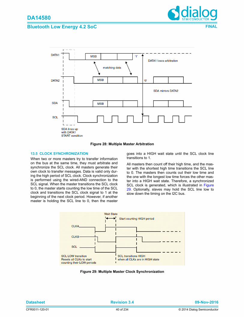
Datasheet Revision 3.4 09-Nov-2016
CFR0011-120-01 40 of 234 © 2014 Dialog Semiconductor
DA14580
Bluetooth Low Energy 4.2 SoC FINAL
13.5 CLOCK SYNCHRONIZATION
When two or more masters try to transfer informationon the bus at the same time, they must arbitrate andsynchronize the SCL clock. All masters generate theirown clock to transfer messages. Data is valid only dur-ing the high period of SCL clock. Clock synchronizationis performed using the wired-AND connection to theSCL signal. When the master transitions the SCL clockto 0, the master starts counting the low time of the SCLclock and transitions the SCL clock signal to 1 at thebeginning of the next clock period. However, if anothermaster is holding the SCL line to 0, then the master
goes into a HIGH wait state until the SCL clock linetransitions to 1.
All masters then count off their high time, and the mas-ter with the shortest high time transitions the SCL lineto 0. The masters then counts out their low time andthe one with the longest low time forces the other mas-ter into a HIGH wait state. Therefore, a synchronizedSCL clock is generated, which is illustrated in Figure29. Optionally, slaves may hold the SCL line low toslow down the timing on the I2C bus.
Figure 28: Multiple Master Arbitration
Figure 29: Multiple Master Clock Synchronization

Datasheet Revision 3.4 09-Nov-2016
CFR0011-120-01 41 of 234 © 2014 Dialog Semiconductor
DA14580
Bluetooth Low Energy 4.2 SoC FINAL
13.6 OPERATION MODES
This section provides information on the following top-ics:
• Slave mode operation
• Master mode operation
• Disabling I2C Controller
Note 5: It is important to note that the I2C Controller should only be
set to operate as an I2C Master, or I2C Slave, but not both
simultaneously. This is achieved by ensuring that bit 6
(I2C_SLAVE_DISABLE) and 0 (I2C_MASTER_MODE) of
the I2C_CON register are never set to 0 and 1, respectively.
13.6.1 Slave Mode Operation
This section includes the following procedures:
• Initial Configuration
• Slave-Transmitter Operation for a Single Byte
• Slave-Receiver Operation for a Single Byte
• Slave-Transfer Operation For Bulk Transfers
Initial Configuration
To use the I2C Controller as a slave, perform the fol-lowing steps:
1. Disable the I2C Controller by writing a ‘0’ to bit 0 ofthe I2C_ENABLE register.
2. Write to the I2C_SAR register (bits 9:0) to set theslave address. This is the address to which the I2CController responds.
3. Write to the I2C_CON register to specify which typeof addressing is supported (7- or 10-bit by setting bit 3).Enable the I2C Controller in slave-only mode by writinga ‘0’ into bit 6 (I2C_SLAVE_DISABLE) and a ‘0’ to bit 0(MASTER_MODE).
Note 6: Slaves and masters do not have to be programmed with the
same type of addressing 7- or 10-bit address. For instance, a
slave can be programmed with 7-bit addressing and a mas-
ter with 10-bit addressing, and vice versa.
4. Enable the I2C Controller by writing a ‘1’ in bit 0 ofthe I2C_ENABLE register.
Note 7: Depending on the reset values chosen, steps 2 and 3 may
not be necessary because the reset values can be config-
ured. For instance, if the device is only going to be a master,
there would be no need to set the slave address because
you can configure the I2C Controller to have the slave dis-
abled after reset and to enable the master after reset. The
values stored are static and do not need to be repro-
grammed if the I2C Controller is disabled.
Slave-Transmitter Operation for a Single Byte
When another I2C master device on the bus addressesthe I2C Controller and requests data, the I2C Controlleracts as a slave-transmitter and the following stepsoccur:
1. The other I2C master device initiates an I2C transferwith an address that matches the slave address in theI2C_SAR register of the I2C Controller.
2. The I2C Controller acknowledges the sent addressand recognizes the direction of the transfer to indicatethat it is acting as a slave-transmitter.
3. The I2C Controller asserts the RD_REQ interrupt (bit5 of the I2C_RAW_INTR_STAT register) and holds theSCL line low. It is in a wait state until softwareresponds. If the RD_REQ interrupt has been masked,due to I2C_INTR_MASK[5] register (M_RD_REQ bitfield) being set to 0, then it is recommended that ahardware and/or software timing routine be used toinstruct the CPU to perform periodic reads of theI2C_RAW_INTR_STAT register.
a. Reads that indicate I2C_RAW_INTR_STAT[5](R_RD_REQ bit field) being set to 1 must be treated asthe equivalent of the RD_REQ interrupt beingasserted.
b. Software must then act to satisfy the I2C transfer.
c. The timing interval used should be in the order of 10times the fastest SCL clock period the I2C Controllercan handle. For example, for 400 kb/s, the timing inter-val is 25us.
Note 8: The value of 10 is recommended here because this is
approximately the amount of time required for a single byte
of data transferred on the I2C bus.
4. If there is any data remaining in the TX FIFO beforereceiving the read request, then the I2C Controllerasserts a TX_ABRT interrupt (bit 6 of theI2C_RAW_INTR_STAT register) to flush the old datafrom the TX FIFO.
Note 9: Because the I2C Controller’s TX FIFO is forced into a
flushed/reset state whenever a TX_ABRT event occurs, it is
necessary for software to release the I2C Controller from this
state by reading the I2C_CLR_TX_ABRT register before
attempting to write into the TX FIFO. See register
I2C_RAW_INTR_STAT for more details.
If the TX_ABRT interrupt has been masked, due to ofI2C_INTR_MASK[6] register (M_TX_ABRT bit field)being set to 0, then it is recommended that re-using thetiming routine (described in the previous step), or asimilar one, be used to read theI2C_RAW_INTR_STAT register.
a. Reads that indicate bit 6 (R_TX_ABRT) being set to1 must be treated as the equivalent of the TX_ABRTinterrupt being asserted.
b. There is no further action required from software.
c. The timing interval used should be similar to thatdescribed in the previous step for theI2C_RAW_INTR_STAT[5] register.
5. Software writes to the I2C_DATA_CMD register withthe data to be written (by writing a ‘0’ in bit 8).
6. Software must clear the RD_REQ and TX_ABRTinterrupts (bits 5 and 6, respectively) of theI2C_RAW_INTR_STAT register before proceeding.
Datasheet Revision 3.4 09-Nov-2016
CFR0011-120-01 42 of 234 © 2014 Dialog Semiconductor
DA14580
Bluetooth Low Energy 4.2 SoC FINAL
If the RD_REQ and/or TX_ABRT interrupts have beenmasked, then clearing of the I2C_RAW_INTR_STATregister will have already been performed when eitherthe R_RD_REQ or R_TX_ABRT bit has been read as1.
7. The I2C Controller releases the SCL and transmitsthe byte.
8. The master may hold the I2C bus by issuing aRESTART condition or release the bus by issuing aSTOP condition.
Slave-Receiver Operation for a Single Byte
When another I2C master device on the bus addressesthe I2C Controller and is sending data, the I2C Control-ler acts as a slave-receiver and the following stepsoccur:
1. The other I2C master device initiates an I2C transferwith an address that matches the I2C Controller’s slaveaddress in the I2C_SAR register.
2. The I2C Controller acknowledges the sent addressand recognizes the direction of the transfer to indicatethat the I2C Controller is acting as a slave-receiver.
3. I2C Controller receives the transmitted byte andplaces it in the receive buffer.
Note 10: If the RX FIFO is completely filled with data when a byte is
pushed, then an overflow occurs and the I2C Controller con-
tinues with subsequent I2C transfers. Because a NACK is
not generated, software must recognize the overflow when
indicated by the I2C Controller (by the R_RX_OVER bit in
the I2C_INTR_STAT register) and take appropriate actions
to recover from lost data. Hence, there is a real time con-
straint on software to service the RX FIFO before the latter
overflow as there is no way to re-apply pressure to the
remote transmitting master. You must select a deep enough
RX FIFO depth to satisfy the interrupt service interval of their
system.
4. I2C Controller asserts the RX_FULL interrupt(I2C_RAW_INTR_STAT[2] register).
If the RX_FULL interrupt has been masked, due to set-ting I2C_INTR_MASK[2] register to 0 or settingI2C_TX_TL to a value larger than 0, then it is recom-mended that a timing routine (described in “Slave-Transmitter Operation for a Single Byte”) be imple-mented for periodic reads of the “I2C_STATUS” onpage 138 register. Reads of the I2C_STATUS register,with bit 3 (RFNE) set at 1, must then be treated by soft-ware as the equivalent of the RX_FULL interrupt beingasserted.
5. Software may read the byte from theI2C_DATA_CMD register (bits 7:0).
6. The other master device may hold the I2C bus byissuing a RESTART condition or release the bus byissuing a STOP condition.
Slave-Transfer Operation for Bulk Transfers
In the standard I2C protocol, all transactions are singlebyte transactions and the programmer responds to a
remote master read request by writing one byte into theslave’s TX FIFO. When a slave (slave-transmitter) isissued with a read request (RD_REQ) from the remotemaster (master-receiver), at a minimum there shouldbe at least one entry placed into the slave-transmitter’sTX FIFO.
I2C Controller is designed to handle more data in theTX FIFO so that subsequent read requests can takethat data without raising an interrupt to get more data.Ultimately, this eliminates the possibility of significantlatencies being incurred between raising the interruptfor data each time had there been a restriction of hav-ing only one entry placed in the TX FIFO.
This mode only occurs when I2C Controller is acting asa slave-transmitter. If the remote master acknowledgesthe data sent by the slave-transmitter and there is nodata in the slave’s TX FIFO, the I2C Controller holdsthe I2C SCL line low while it raises the read requestinterrupt (RD_REQ) and waits for data to be writteninto the TX FIFO before it can be sent to the remotemaster.
If the RD_REQ interrupt is masked, due to bit 5(M_RD_REQ) of the I2C_INTR_STAT register beingset to 0, then it is recommended that a timing routinebe used to activate periodic reads of theI2C_RAW_INTR_STAT register. Reads ofI2C_RAW_INTR_STAT that return bit 5 (R_RD_REQ)set to 1 must be treated as the equivalent of theRD_REQ interrupt referred to in this section. This tim-ing routine is similar to that described in “Slave-Trans-mitter Operation for a Single Byte”
The RD_REQ interrupt is raised upon a read request,and like interrupts, must be cleared when exiting theinterrupt service handling routine (ISR). The ISR allowsyou to either write 1 byte or more than 1 byte into theTX FIFO. During the transmission of these bytes to themaster, if the master acknowledges the last byte. thenthe slave must raise the RD_REQ again because themaster is requesting for more data.
If the programmer knows in advance that the remotemaster is requesting a packet of n bytes, then whenanother master addresses I2C Controller and requestsdata, the TX FIFO could be written with n number bytesand the remote master receives it as a continuousstream of data. For example, the I2C Controller slavecontinues to send data to the remote master as long asthe remote master is acknowledging the data sent andthere is data available in the TX FIFO. There is noneed to hold the SCL line low or to issue RD_REQagain.
If the remote master is to receive n bytes from the I2CController but the programmer wrote a number of byteslarger than n to the TX FIFO, then when the slave fin-ishes sending the requested n bytes, it clears the TXFIFO and ignores any excess bytes.
The the I2C Controller generates a transmit abort(TX_ABRT) event to indicate the clearing of the TXFIFO in this example. At the time an ACK/NACK isexpected, if a NACK is received, then the remote mas-

Datasheet Revision 3.4 09-Nov-2016
CFR0011-120-01 43 of 234 © 2014 Dialog Semiconductor
DA14580
Bluetooth Low Energy 4.2 SoC FINAL
ter has all the data it wants. At this time, a flag is raisedwithin the slave’s state machine to clear the leftoverdata in the TX FIFO. This flag is transferred to the pro-cessor bus clock domain where the FIFO exists andthe contents of the TX FIFO is cleared at that time.
13.6.2 Master Mode Operation
This section includes the following topics:
• Initial Configuration
• Master Transmit and Master Receive
Initial Configuration
The procedures are very similar and are only differentwith regard to where the I2C_10BITADDR_MASTERbit is set (either bit 4 of I2C_CON register or bit 12 ofI2C_TAR register).
To use the I2C Controller as a master perform the fol-lowing steps:
1. Disable the I2C Controller by writing 0 to theI2C_ENABLE register.
2. Write to the I2C_CON register to set the maximumspeed mode supported (bits 2:1) and the desiredspeed of the I2C Controller master-initiated transfers,either 7-bit or 10-bit addressing (bit 4).
Ensure that bit 6 I2C_SLAVE_DISABLE = 1 and bit 0MASTER_MODE =1
Note 11: Slaves and masters do not have to be programmed with the
same type of addressing 7- or 10-bit address. For instance, a
slave can be programmed with 7-bit addressing and a mas-
ter with 10-bit addressing, and vice versa.
3. Write to the I2C_TAR register the address of the I2Cdevice to be addressed (bits 9:0). This register alsoindicates whether a General Call or a START BYTEcommand is going to be performed by I2C.
4. Only applicable for high-speed mode transfers. Writeto the I2C_HS_MADDR register the desired mastercode for the I2C Controller. The master code is pro-grammer-defined.
5. Enable the I2C Controller by writing a 1 in bit 0 of theI2C_ENABLE register.
6. Now write transfer direction and data to be sent tothe I2C_DATA_CMD register. If the I2C_DATA_CMDregister is written before the I2C Controller is enabled,the data and commands are lost as the buffers are keptcleared when I2C Controller is disabled.
This step generates the START condition and theaddress byte on the I2C Controller. Once I2C Control-ler is enabled and there is data in the TX FIFO, I2CController starts reading the data.
Note 12: Depending on the reset values chosen, steps 2, 3, 4, and 5
may not be necessary because the reset values can be con-
figured. The values stored are static and do not need to be
reprogrammed if the I2C Controller is disabled, with the
exception of the transfer direction and data.
Master Transmit and Master Receive
The I2C Controller supports switching back and forthbetween reading and writing dynamically. To transmitdata, write the data to be written to the lower byte of theIC_DATA_CMD register. The CMD bit [8] should bewritten to 0 for I2C write operations.
Subsequently, a read command may be issued by writ-ing “don’t cares” to the lower byte of theIC_DATA_CMD register, and a 1 should be written tothe CMD bit.
The I2C Controller master continues to initiate trans-fers as long as there are commands present in thetransmit FIFO. If the transmit FIFO becomes empty, themaster inserts a STOP condition after completing thecurrent transfer.
13.6.3 Disabling the I2C Controller
The register I2C_ENABLE_STATUS is added to allowsoftware to unambiguously determine when the hard-ware has completely shutdown in response to theI2C_ENABLE register being set from 1 to 0. Only oneregister is required to be monitored
Procedure
1. Define a timer interval (ti2c_poll) equal to the 10times the signalling period for the highest I2C transferspeed used in the system and supported by I2C Con-troller. For example, if the highest I2C transfer mode is400 kb/s, then this ti2c_poll is 25us.
2. Define a maximum time-out parameter,MAX_T_POLL_COUNT, such that if any repeated poll-ing operation exceeds this maximum value, an error isreported.
3. Execute a blocking thread/process/function that pre-vents any further I2C master transactions to be startedby software, but allows any pending transfers to becompleted.
Note 13: This step can be ignored if I2C Controller is programmed to
operate as an I2C slave only.
4. The variable POLL_COUNT is initialized to zero.
5. Set I2C_ENABLE to 0.
6. Read the I2C_ENABLE_STATUS register and testthe I2C_EN bit (bit 0). Increment POLL_COUNT byone. If POLL_COUNT >= MAX_T_POLL_COUNT, exitwith the relevant error code.
7. If I2C_ENABLE_STATUS[0] is 1, then sleep forti2c_poll and proceed to the previous step.
Otherwise, exit with a relevant success code.

Datasheet Revision 3.4 09-Nov-2016
CFR0011-120-01 44 of 234 © 2014 Dialog Semiconductor
DA14580
Bluetooth Low Energy 4.2 SoC FINAL
14 UARTThe DA14580 contains two identical instances of thisblock, i.e. UART and UART2.
The UART is compliant to the industry-standard 16550and is used for serial communication with a peripheral,modem (data carrier equipment, DCE) or data set.Data is written from a master (CPU) over the APB busto the UART and it is converted to serial form andtransmitted to the destination device. Serial data is alsoreceived by the UART and stored for the master (CPU)to read back.
There is no DMA support on the UART block since itscontains internal FIFOs. Both UARTs support hardwareflow control signals (RTS, CTS, DTR, DSR).
Features
• 16 bytes Transmit and receive FIFOs
• Hardware flow control support (CTS/RTS)
• Shadow registers to reduce software overhead and also include a software programmable reset
• Transmitter Holding Register Empty (THRE) inter-rupt mode
• IrDA 1.0 SIR mode supporting low power mode.
• Functionality based on the 16550 industry standard:
• Programmable character properties, such as num-ber of data bits per character (5-8), optional
• parity bit (with odd or even select) and number of stop bits (1, 1.5 or 2)
• Line break generation and detection
• Prioritized interrupt identification
• Programmable serial data baud rate as calculated by the following: baud rate = (serial clock frequency)/(divisor).
Figure 30: UART Block Diagram
UARTUART2
Serial Receiver Serial Transmitter
Baud Clock
Generator
Timeout Detector
Sync Block
Modem Sync Block
Register Block
APB Interface
FIFO Block
pclk
cts_n
APB Bus
uart_clk
uart_rx uart_tx
rts_n
uart_int

Datasheet Revision 3.4 09-Nov-2016
CFR0011-120-01 45 of 234 © 2014 Dialog Semiconductor
DA14580
Bluetooth Low Energy 4.2 SoC FINAL
14.1 UART (RS232) SERIAL PROTOCOL
Because the serial communication between the UARTand the selected device is asynchronous, additionalbits (start and stop) are added to the serial data to indi-cate the beginning and end. Utilizing these bits allowstwo devices to be synchronized. This structure of serialdata accompanied by start and stop bits is referred toas a character, as shown in Figure 31.
An additional parity bit may be added to the serial char-acter. This bit appears after the last data bit and beforethe stop bit(s) in the character structure to provide theUART with the ability to perform simple error checkingon the received data.
The UART Line Control Register (UART_LCR_REG) isused to control the serial character characteristics. Theindividual bits of the data word are sent after the startbit, starting with the least-significant bit (LSB). Theseare followed by the optional parity bit, followed by thestop bit(s), which can be 1, 1.5 or 2.
All the bits in the transmission (with exception to thehalf stop bit when 1.5 stop bits are used) are transmit-
ted for exactly the same time duration. This is referredto as a Bit Period or Bit Time. One BitTime equals 16baud clocks. To ensure stability on the line the receiversamples the serial input data at approximately the midpoint of the Bit Time once the start bit has beendetected. As the exact number of baud clocks thateach bit was transmitted for is known, calculating themid point for sampling is not difficult, that is every 16baud clocks after the mid point sample of the start bit.Figure 32 shows the sampling points of the first coupleof bits in a serial character.
As part of the 16550 standard an optional baud clockreference output signal (baudout_n) is supplied to pro-vide timing information to receiving devices that requireit. The baud rate of the UART is controlled by the serialclock (sclk or pclk in a single clock implementation) andthe Divisor Latch Register (DLH and DLL).
14.2 IRDA 1.0 SIR PROTOCOL
The Infrared Data Association (IrDA) 1.0 Serial Infrared(SIR) mode supports bi-directional data communica-tions with remote devices using infrared radiation asthe transmission medium. IrDA 1.0 SIR mode specifiesa maximum baud rate of 115.2 kBaud.
Note 14: Attention. Information provided on IrDA SIR mode in this
section assumes that the reader is fully familiar with the IrDA
Serial Infrared Physical Layer Specifications. This specifica-
tion can be obtained from the following website:
http://www.irda.org
The data format is similar to the standard serial (soutand sin) data format. Each data character is sent seri-ally, beginning with a start bit, followed by 8 data bits,and ending with at least one stop bit. Thus, the numberof data bits that can be sent is fixed. No parity informa-tion can be supplied and only one stop bit is used whilein this mode.
Trying to adjust the number of data bits sent or enable
Figure 31: Serial Data Format
Figure 32: Receiver Serial Data Sampling Points

Datasheet Revision 3.4 09-Nov-2016
CFR0011-120-01 46 of 234 © 2014 Dialog Semiconductor
DA14580
Bluetooth Low Energy 4.2 SoC FINAL
parity with the Line Control Register (LCR) has noeffect. When the UART is configured to support IrDA1.0 SIR it can be enabled with Mode Control Register(MCR) bit 6. When the UART is not configured to sup-port IrDA SIR mode, none of the logic is implementedand the mode cannot be activated, reducing total gatecounts. When SIR mode is enabled and active, serialdata is transmitted and received on the sir_out_n andsir_in ports, respectively.
Transmitting a single infrared pulse signals a logiczero, while a logic one is represented by not sending a
pulse. The width of each pulse is 3/16th of a normalserial bit time. Thus, each new character begins withan infrared pulse for the start bit. However, receiveddata is inverted from transmitted data due to the infra-red pulses energizing the photo transistor base of theIrDA receiver, pulling its output low. This inverted tran-sistor output is then fed to the UART sir_in port, whichthen has correct UART polarity. Figure 33 shows thetiming diagram for the IrDA SIR data format in compar-ison to the standard serial format.
As detailed in the IrDA 1.0 SIR, the UART can be con-figured to support a low-power reception mode. Whenthe UART is configured in this mode, the reception ofSIR pulses of 1.41 s (minimum pulse duration) is pos-sible, as well as nominal 3/16th of a normal serial bittime. Using this low-power reception mode requiresprogramming the Low Power Divisor Latch (LPDLL/LPDLH) registers. It should be noted that for all sclkfrequencies greater than or equal to 7.37 MHz (andobey the requirements of the Low Power Divisor Latchregisters), pulses of 1.41 s are detectable. Howeverthere are several values of sclk that do not allow thedetection of such a narrow pulse and these are as fol-lows:
When IrDA SIR mode is enabled, the UART operationis similar to when the mode is disabled, with oneexception; data transfers can only occur in half-duplexfashion when IrDA SIR mode is enabled. This isbecause the IrDA SIR physical layer specifies a mini-mum of 10 ms delay between transmission and recep-tion. This 10 ms delay must be generated by software.
14.3 CLOCK SUPPORT
The UART has two system clocks (pclk and sclk). Hav-ing the second asynchronous serial clock (sclk) imple-mented accommodates accurate serial baud ratesettings, as well as APB bus interface requirements.
With the two clock design a synchronization module isimplemented for synchronization of all control and dataacross the two system clock boundaries.
A serial clock faster than four-times the PCLK does notleave enough time for a complete incoming characterto be received and pushed into the receiver FIFO.However, in most cases, the PCLK signal is faster thanthe serial clock and this should never be an issue.
The serial clock modules must have time to see newregister values and reset their respective statemachines. This total time is guaranteed to be no morethan eight clock cycles of the slower of the two systemclocks. Therefore, no data should be transmitted orreceived before this maximum time expires, after initialconfiguration.
For a clear view of the baud rate generation and theconstraints, please refer to section 11.4.
Figure 33: IrDA SIR Data Format
Table 20: Low Power Divisor Latch Register Values
SCLKLow Power Divisor Latch Register Value
Min. Pulse Width for Detection
1.84 MHz 1 3.77 s
3.69 MHz 2 2.086 s
5.33 MHz 3 1.584 s

Datasheet Revision 3.4 09-Nov-2016
CFR0011-120-01 47 of 234 © 2014 Dialog Semiconductor
DA14580
Bluetooth Low Energy 4.2 SoC FINAL
14.4 INTERRUPTS
The assertion of the UART interrupt (UART_INT)occurs whenever one of the several prioritized interrupttypes are enabled and active. The following interrupttypes can be enabled with the IER register:
• Receiver Error
• Receiver Data Available
• Character Timeout (in FIFO mode only)
• Transmitter Holding Register Empty at/below thresh-old (in Programmable THRE interrupt mode)
When an interrupt occurs the master accesses theUART_IIR_REG to determine the source of the inter-rupt before dealing with it accordingly. These interrupttypes are described in more detail in Table 21.
14.5 PROGRAMMABLE THRE INTERRUPT
The UART can be configured to have a ProgrammableTHRE Interrupt mode available to increase system per-formance.
When Programmable THRE Interrupt mode is selectedit can be enabled via the Interrupt Enable Register(IER[7]). When FIFOs and the THRE Mode are imple-mented and enabled, THRE Interrupts are active at,and below, a programmed transmitter FIFO emptythreshold level, as opposed to empty, as shown in theflowchart in Figure 34.
Table 21: UART Interrupt Priorities
Interrupt Id Interrupt Set and Reset Functions
Bits [3-0]PriorityLevel
Interrupt Type Interrupt Source Interrupt Reset Control
0001 - None
0110 Highest Receiver Line status Overrun/parity/ framing errors or break interrupt
Reading the line status reg-ister
0100 1 Receiver Data Available Receiver data available (non-FIFO mode or FIFOs disabled) orRCVR FIFO trigger level reached (FIFO mode and FIFOs enabled)
Reading the receiver buffer register (non-FIFO mode or FIFOs disabled) or the FIFO drops below the trigger level (FIFO mode and FIFOs enabled)
1100 2 Character timeout indi-cation
No characters in or out of the RCVR FIFO during the last 4 character times and there is at least 1 character in it during this time.
Reading the receiver buffer register
0010 3 Transmitter holding reg-ister empty
Transmitter holding register empty (Prog. THRE Mode dis-abled) or XMIT FIFO at or below threshold (Prog. THRE Mode enabled).
Reading the IIR register (if source of interrupt); or, writ-ing into THR (FIFOs or THRE Mode not selected or disabled) or XMIT FIFO above threshold (FIFOs and THRE Mode selected and enabled).
0000 4 Reserved
0111 Lowest Reserved - -

Datasheet Revision 3.4 09-Nov-2016
CFR0011-120-01 48 of 234 © 2014 Dialog Semiconductor
DA14580
Bluetooth Low Energy 4.2 SoC FINAL
This threshold level is programmed into FCR[5:4]. Theavailable empty thresholds are: empty, 2, ¼ and ½.See UART_FCR_REG for threshold setting details.Selection of the best threshold value depends on thesystem's ability to begin a new transmission sequencein a timely manner. However, one of these thresholdsshould prove optimum in increasing system perfor-mance by preventing the transmitter FIFO from runningempty.
In addition to the interrupt change, Line Status Register(LSR[5]) also switches function from indicating trans-mitter FIFO empty, to FIFO full. This allows software tofill the FIFO each transmit sequence by polling LSR[5]before writing another character. The flow thenbecomes, “fill transmitter FIFO whenever an interrupt
occurs and there is data to transmit”, instead of waitinguntil the FIFO is completely empty. Waiting until theFIFO is empty causes a performance hit whenever thesystem is too busy to respond immediately.
Even if everything else is selected and enabled, if theFIFOs are disabled via FCR[0], the ProgrammableTHRE Interrupt mode is also disabled. When notselected or disabled, THRE interrupts and LSR[5] func-tion normally (both reflecting an empty THR or FIFO).The flowchart of THRE interrupt generation when not inprogrammable THRE interrupt mode is shown inFigure 35.
Figure 34: Flowchart of Interrupt Generation for Programmable THRE Interrupt Mode
Figure 35: Flowchart of Interrupt Generation When Not in Programmable THRE Interrupt Mode

Datasheet Revision 3.4 09-Nov-2016
CFR0011-120-01 49 of 234 © 2014 Dialog Semiconductor
DA14580
Bluetooth Low Energy 4.2 SoC FINAL
14.6 SHADOW REGISTERS
The shadow registers shadow some of the existingregister bits that are regularly modified by software.These can be used to reduce the software overheadthat is introduced by having to perform read-modifywrites.
• UART_SRBR_REG support a host burst mode where the host increments it address but still accesses the same Receive buffer register
• UART_STHR support a host burst mode where the host increments it address but still accesses the same transmit holding register.
• UART_SFE_REG accesses the FCR[0] register without accessing the other UART_FCR_REG bits.
• UART_SRT_REG accesses the FCR[7-6] register without accessing the other UART_FCR_REG bits.
• UART_STER_REG accesses the FCR[5-4] register without accessing the other UART_FCR_REG bits.
14.7 DIRECT TEST MODE
The on-chip UARTS can be used for the Direct TestMode required for the final product PHY layer testing. Itcan be done either over the HCI layer, which engagesa full CTS/RTS UART or using a 2-wire UART directlyas described in the Bluetooth Low Energy Specification(Volume 6, Part F).

Datasheet Revision 3.4 09-Nov-2016
CFR0011-120-01 50 of 234 © 2014 Dialog Semiconductor
DA14580
Bluetooth Low Energy 4.2 SoC FINAL
15 SPI+ InterfaceThis interface supports a subset of the Serial Periph-eral Interface (SPITM). The serial interface can transmitand receive 8, 16 or 32 bits in master/slave mode andtransmit 9 bits in master mode. The SPI+ interface hasenhanced functionality with bidirectional 2x16-bit wordFIFOs.
SPI is a trademark of Motorola, Inc.
Features
• Slave and Master mode
• 8 bit, 9 bit, 16 bit or 32 bit operation
• Clock speeds up to 16 MHz for the SPI controller. Programmable output frequencies of SPI source clock divided by 1, 2, 4, 8
• SPI clock line speed up to 8 MHz
• SPI mode 0, 1, 2, 3 support (clock edge and phase)
• Programmable SPI_DO idle level
• Maskable Interrupt generation
• Bus load reduction by unidirectional writes-only and reads-only modes.
• Built-in RX/TX FIFOs for continuous SPI bursts.
15.1 OPERATION WITHOUT FIFOS
This mode is the default mode.
Master Mode
To enable SPITM operation, first the individual port sig-nal must be enabled. Next the SPI must be configuredin SPI_CTRL_REG, for the desired mode. Finally bitSPI_ON must be set to 1.
A SPI transfer cycle starts after writing to theSPI_RX_TX_REG0. In case of 32 bits mode, theSPI_RX_TX_REG1 must be written first. Writing toSPI_RX_TX_REG0 also sets the SPI_TXH. As soonas the holding register is copied to the IO buffer, theSPI_TXH is reset and a serial transfer cycle of 8/9/16/32 clock-cycles is started which causes 8/9/16/32 bits
to be transmitted on SPI_DO. Simultaneously, data isreceived on SPI_DI and shifted into the IO buffer. Thetransfer cycle finishes after the 8th/9th/16th/32nd clockcycle and SPI_INT_BIT bit is set in theSPI_CTRL_REG and SPI_INT_PEND bit in(RE)SET_INT_PENDING_REG is set. The receivedbits in the IO buffer are copied to theSPI_RX_TX_REG0 (and SPI_RX_TX_REG1 in caseof 32 bits mode) were they can be read by the CPU.
Interrupts to the ICU can be disabled using theSPI_MINT bit. To clear the SPI interrupt source, anyvalue to SPI_CLEAR_INT_REG must be written. Notehowever that SPI_INT will be set as long as the RX-FIFO contains unread data.
Figure 36: SPI Block Diagram
SPI_TX_REG0 SPI_TX_REG1
SPI_RX_REG0 SPI_RX_REG1
IO buffer
SPI_SMn
SPI_CLK
SPI clock SPI_DO
APB bus
APB bus
SPI_CLK SPI_DO SPI_DI
Px_MODE_REG[]
SPI_PHA SPI_POL
SPI_RST
SPI_FORCE_DO
SPI_ON
SPI_MINT
SPI_EN
SPI_EN_CTRL
Port x
SPI_INT
tx_req
rx_req
TX-FIFO
RX-FIFO
Request &
SelectionInterrupt
clear_tx_req
clear_rx_req
SPI_9BIT_VAL

Datasheet Revision 3.4 09-Nov-2016
CFR0011-120-01 51 of 234 © 2014 Dialog Semiconductor
DA14580
Bluetooth Low Energy 4.2 SoC FINAL
Slave Mode
The slave mode is selected with SPI_SMn set to 1 andthe Px_MODE_REG must also select SPI_CLK asinput. The functionality of the IO buffer in slave andmaster mode is identical. The SPI module clocks datain on SPI_DI and out on SPI_DO on every active edgeof SPI_CLK. As shown in Figure 37 to Figure 40. TheSPI has an active low clock enable SPI_EN, which canbe enabled with bit SPI_EN_CTRL=1.
In slave mode the internal SPI clock must be more thanfour times the SPI_CLK
In slave mode the SPI_EN serves as a clock enableand bit synchronization If enabled with bitSPI_EN_CTRL. As soon as SPI_EN is deactivatedbetween the MSB and LSB bits, the I/O buffer is reset.
SPI_POL and SPI_PHA
The phase and polarity of the serial clock can bechanged with bits SPI_POL and SPI_PHA in theSPI_CTRL_REG.
SPI_DO Idle Levels
The idle level of signal SPI_DO depends on the masteror slave mode and polarity and phase mode of theclock.
In master mode pin SPI_DO gets the value of bitSPI_DO if the SPI is idle in all modes. Also if slave inSPI modes 0 and 2, SPI_DO is the initial and final idlelevel.
In SPI modes 1 and 3 however there is no clock edgeafter the sampled lsb and pin SPI_DO gets the lsbvalue of the IO buffer. If required, the SPI_DO can beforced to the SPI_DO bit level by resetting the SPI tothe idle state by shortly setting bit SPI_RST to 1.(Optionally SPI_FORCE_DO can be set, but this doesnot reset the IO buffer). The following diagrams show
the timing of the SPITM interface.
Writes Only Mode
In “writes only” mode (SPI_FIFO_MODE = “10“) onlythe TX-FIFO is used. Received data will be copied tothe SPI_RX_TX_REGx, but if a new SPI transfer is fin-ished before the old data is read from the memory, thisregister will be overwritten.
SPI_INT acts as a tx_request signal, indicating thatthere is still place in the FIFO. It will be ‘0’ when theFIFO is full or else ‘1’ when it’s not full. This is also indi-cated in the SPI_CTRL_REG[SPI_TXH], which is ‘1’ ifthe TX-FIFO is full. Writing to the FIFO if this bit is still1, will result in transmission of undefined data. If alldata has been transferred, SPI_CTRL_REG1[SPI_BUSY] will become ‘0’.
Reads Only Mode
In “reads only” mode (SPI_FIFO_MODE = “01“) onlythe RX-FIFO is used. Transfers will start immediatelywhen the SPI is turned on in this mode. In transmitdirection the SPI_DO pin will transmit the IO buffercontents being the actual value of the SPI_TX_REGx
(all 0’s after reset). This means that no dummy writesare needed for reads only transfers.
In Slave Mode transfers only take place if the externalmaster initiates them, but in master mode this meansthat transfers will continue until the RX-FIFO is full. Ifthis happens SPI_CTRL_REG1[SPI_BUSY] willbecome ‘0’. If exactly N words need to be read fromSPI device, first read (N - fifosize+1) words. Then waituntil the SPI_BUSY becomes ‘0’, setSPI_FIFO_MODE to “00” and finally read the remain-ing (fifosize +1) words. Here fifosize is 4/2/1 words for8/16/32 bits mode respectively.
If this is not done, more data will be read from the SPIdevice until the FIFO is completely filled, or the SPI isturned off.
Bidirectional Transfers with FIFO
If SPI_FIFO_MODE is “00“, both registers are used asa FIFO. SPI_TXH indicates that TX-FIFO is full,SPI_INT indicates that there is data in the RX-FIFO.
15.2 9 BITS MODE
The 9 bits mode can be used to support 9 bits displaysand is selected with SPI_CTRL_REG[SPI_WORD] setto ‘11’. The value of the 9th bit, set in theSPI_CTRL_REG1[SPI_9BIT_VAL] and is used todetermine if the next 8 bits form a command word ordata word. Because the 9th bit is not part of the data,the FIFOs are still used in the 8 bits mode. The 9th bitis received but not saved because it is shifted out of the8 bits shift register upon reception.

Datasheet Revision 3.4 09-Nov-2016
CFR0011-120-01 52 of 234 © 2014 Dialog Semiconductor
DA14580
Bluetooth Low Energy 4.2 SoC FINAL
Note 15: If 9 bits SPI mode, the MSB bit in transmit direction is determined by bit SPI_CTRL_REG[SPI_9BIT_VAL]. In receive direction, the MSB is
received but not stored.
For the MSB bit refer to note 15.
Figure 37: SPI Master/Slave, Mode 0: SPI_POL=0 and SPI_PHA=0
SPI_DO MSB LSB SPI_DO
SPI_DO MSB LSB SPI_DO
MSB LSB SPI_DO
MSB LSB
^ write to SPI_RX_TX_REG0
^ write to SPI_RX_TX_REG0
SPI_CLK
SPI_DO (Master)
SPI_DO 1 (Slave)
SPI_DO 2 (Slave)
SPI_DI
SPI_EN (Slave)
Figure 38: SPI Master/Slave, Mode 1: SPI_POL=0 and SPI_PHA=1
SPI_DO MSB LSB SPI_DO
SPI_DO MSB LSB
MSB LSB
^ write to SPI_RX_TX_REG0
SPI_CLK
SPI_DO (Master)
SPI_DO (Slave)
SPI_DI
SPI_EN (Slave)

Datasheet Revision 3.4 09-Nov-2016
CFR0011-120-01 53 of 234 © 2014 Dialog Semiconductor
DA14580
Bluetooth Low Energy 4.2 SoC FINAL
For the MSB bit refer to note 15.
For the MSB bit refer to note 15.
Figure 39: SPI Master/Slave, Mode 2: SPI_POL=1 and SPI_PHA=0
SPI_DO MSB LSB SPI_DO
SPI_DO MSB LSB SPI_DO
MSB LSB SPI_DO
MSB LSB
^ write to SPI_RX_TX_REG0
^ write to SPI_RX_TX_REG0
SPI_CLK
SPI_DO (Master)
SPI_DO 1 (Slave)
SPI_DO 2 (Slave)
SPI_DI
SPI_EN (Slave)
Figure 40: SPI Master/Slave, Mode 3: SPI_POL=1 and SPI_PHA=1
SPI_DO MSB LSB SPI_DO
SPI_DO MSB LSB
MSB LSB
^ write to SPI_RX_TX_REG0
SPI_CLK
SPI_DO (Master)
SPI_DO (Slave)
SPI_DI
SPI_EN (Slave)

Datasheet Revision 3.4 09-Nov-2016
CFR0011-120-01 54 of 234 © 2014 Dialog Semiconductor
DA14580
Bluetooth Low Energy 4.2 SoC FINAL
16 Quadrature DecoderThe DA14580 has a integrated quadrature decoderthat can automatically decode the signals for the X, Yand Z axes of a HID input device, reporting step countand direction. This block can be used for waking up thechip as soon as there is any kind of movement from theexternal device connected to it. The block diagram ofthe quadrature decoder is presented in Figure 41.
Features
• Three 16-bit signed counters that provide the step count and direction on each of the axes (X, Y and Z)
• Programmable system clock sampling at maximum 16 MHz.
• APB interface for control and programming
• Programmable source from P0, P1 and P2 ports
• Digital filter on the channel inputs to avoid spikes
Channels are expected to provide a pulse train with 90degrees rotation as displayed in the following figures:
Depending on whether channel A or channel B is lead-ing in phase, the quadrature decoding block calculatesthe direction on the related axis. Furthermore, thesigned counter value represents the number of stepsmoved.
Since six channels are required (two for each axis), allP0 and P1 signals and some of the P2 port can bemapped onto this block. The user can choose whichGPIOs to use for the channels by programming theQDEC_CTRL2_REG register.
The digital filter eliminates any spike shorter than twoclock periods. The counter holds the movement eventsof the channel. When a channel is disabled the counteris reset. The counters are accessible via the APB bus.
The quadrature decoder operates on the system clock.The QDEC_CLOCKDIV register defines the number ofclock cycles of the period at which the decoding logicsamples the data on the channel inputs.
Figure 41: Quadrature Decoder Block Diagram
Figure 42: Moving Forward on Axis X
Register File
16-bit Counter (X Axis)
Dig
ital
Filter
QD_CHA_X
QD_CHB_X
16-bit Counter (Y Axis)
Digital
Filter
QD_CHA_Y
QD_CHB_Y
16-bit Counter (Z Axis)
Digita
l F
ilter
QD_CHA_Z
QD_CHB_Z
Interrupt Generator
APB Interface
Quad_Dec_IRQn
QD_CHA_X
QD_CHB_X
Figure 43: Moving Backwards on Axis X
QD_CHA_X
QD_CHB_X

Datasheet Revision 3.4 09-Nov-2016
CFR0011-120-01 55 of 234 © 2014 Dialog Semiconductor
DA14580
Bluetooth Low Energy 4.2 SoC FINAL
17 Wake-Up TimerThe Wake-up timer can be programmed to wake up theDA14580 from power down mode after a prepro-grammed number of GPIO events.
Each of the GPIO inputs can be selected to generatean event by programming the correspondingWKUP_SELECT_Px_REG register. When allWKUP_SELECT_Px_REG registers are configured togenerate a wake-up interrupt, a toggle on any GPIOwill wake up the system.
The input signal edge can be selected by programmingthe WKUP_POL_Px_REG register.
The block diagram illustrating the Wake-up function isshown in Figure 44.
Features
• Monitors any GPIO state change
• Implements debouncing time from 0 up to 63 ms
• Accumulates external events and compares the number to a programmed value
• Generates an interrupt to the CPU
A LOW to HIGH level transition on the selected inputport, while WKUP_POL_Px_REG[y] = 0, sets internalsignal “key_hit” to ‘1’. This signal triggers the eventcounter state machine as shown in Figure 45. The debounce timer is loaded with valueWKUP_CTRL_REG[WKUP_DEB_VALUE]. The timercounts down every 1 ms. If the timer reaches 0 and the“key_hit” signal is still ‘1’, the event counter will beincremented.
The event counter is edge sensitive. After detecting anactive edge a reverse edge must be detected firstbefore it goes back to the IDLE state and from therestarts waiting for a new active edge.
A minimum pulse duration of 2 sleep clock cycles mustbe applied to the GPIO to ensure a successful systemwake-up.
If the event counter is equal to the value set in theWKUP_COMPARE_REG register, the counter will bereset and an interrupt will be generated, if it wasenabled by WKUP_CTRL_REG[ENABLE_IRQ].
The interrupt can be cleared by writing any value toregister WKUP_RESET_IRQ_REG. The event counter can be reset by writing any value toregister WKUP_RESET_CNTR_REG.The value of the event counter can be read at any timeby reading register WKUP_COUNTER_REG.
Figure 44: Wake-Up Timer Block Diagram
WUPCT_IRQkey_hit
+
DEBOUNCE TIMER EVENTCOUNTER
WKUP_COMPARE_REG
&
P00wkup_pol_p0_reg[0]
wkup_select_p0_reg[0]
>+&
P37wkup_pol_p3_reg[7]
wkup_select_p3_reg[7]
.
.
.
wkup_ctrl_reg[6]
Figure 45: Event Counter State Machine for the Wake-Up Interrupt Generator
IDLE
KEY_PRESSED
key_hit = 1timer = DEBOUNCE
key_hit = 0 andtimer = 0
timer not 0
RST
KEY_RELEASE
key_hit = 1key_hit = 1 and
timer = 0event_count = event_count +1
key_hit = 0

Datasheet Revision 3.4 09-Nov-2016
CFR0011-120-01 56 of 234 © 2014 Dialog Semiconductor
DA14580
Bluetooth Low Energy 4.2 SoC FINAL
18 General Purpose TimersThe Timer block contains 2 timer modules that are soft-ware controlled, programmable and can be used forvarious tasks. Timer 0 is a 16-bit general purpose timerwith a PWM output capability. Timer 2 is a 14-bit coun-ter that generates three identical PWM signals in aquite flexible manner.
18.1 TIMER 0
Timer 0 is a 16-bit general purpose software program-mable timer, which has the ability of generating PulseWidth Modulated signals, namely PWM0 and PWM1. Italso generates the SWTIM_IRQ interrupt to the ARMCortex-M0. It can be configured in various modesregarding output frequency, duty cycle and the modula-tion of the PWM signals.
Features
• 16-bit general purpose timer
• Ability to generate 2 Pulse Width Modulated signals (PWM0 and PWM1)
• Programmable output frequency:
with N = 0 to (216-1), M = 0 to (216-1)
• Programmable duty cycle:
• Separately programmable interrupt timer:
Figure 46 shows the block diagram of Timer 0. The 16bits timer consists of two counters: T0-counter and ON-counter, and three registers:TIMER0_RELOAD_M_REG,TIMER0_RELOAD_N_REG and TIMER0_ON_REG.Upon reset, the counter and register values are0x0000. Timer 0 will generate a Pulse Width Modulatedsignal PWM0. The frequency and duty cycle of PWM0are determined by the contents of theTIMER0_RELOAD_N_REG and theTIMER0_RELOAD_M_REG registers.
The timer can run at five different clocks: 16 MHz,8 MHz, 4 MHz, 2 MHz or 32 kHz. The 32 kHz clock is
selected by default with bit TIM0_CLK_SEL in theTIMER0_CTRL_REG register. This ‘slow’ clock has noenabling bit. The other four options can be selected bysetting the TIM0_CLK_SEL bit and the TMR_ENABLEbit in the CLK_PER_REG (default disabled). This reg-ister also controls the frequency via the TMR_DIV bits.An extra clock divider is available that can be activatedvia bit TIM0_CLK_DIV of the timer control registerTIMER0_CTRL_REG. This clock divider is only usedfor the ON-counter and always divides by 10.
Timer 0 operates in PWM mode. The signals PWM0and PWM1 can be mapped to any GPIOs.
f 16, 8, 4, 2 MHz or 32 kHz M 1+ N 1+ +
------------------------------------------------------------------------=
M 1+M 1+ N 1+ +-------------------------------------------- 100 %=
T 16, 8, 4, 2 MHz or 32 kHz ON 1+
------------------------------------------------------------------------=
Figure 46: Timer 0 Block Diagram
LSBreg Timer 0
MSBreg
TIMER0_RELOAD_N_REG
LSBreg MSBreg
Compare
LSBreg MSBreg
If T0-counter = 0 then T0_toggle = ~T0_toggle
T0_ge_M0TIM0_INT
ON-counter
LSBshadow MSBshadow LSBshadow MSBshadow
loadnewloadnew0 01 1
-1
0 1
T0-counter=0 1 0
1 0loadnew
loadnew
loadnew
LSBreg MSBreg
TIMER0_0N_REG
LSBreg MSBreg
T0-counter
TIMER0_RELOAD_M_REG
T0-toggle
Interrupt generation:PWM mode:
if (T0_toggle=0 andON-counter=0) ORTIM0_CTRL =0->1
December 13, 2012
PWM0
PWM1
to GPIOIf PWM_MODE = 1 then AND signal with clock
If PWM_MODE = 1 then AND signal with clock

Datasheet Revision 3.4 09-Nov-2016
CFR0011-120-01 57 of 234 © 2014 Dialog Semiconductor
DA14580
Bluetooth Low Energy 4.2 SoC FINAL
Timer 0 PWM Mode
If bit TIM0_CTRL in the TIMER0_CTRL_REG is set,Timer 0 will start running. SWTIM_IRQ will be gener-ated and the T0-counter will load its start value fromthe TIMER0_RELOAD_M_REG register, and will dec-rement on each clock. The ON-counter also loads itsstart value from the TIMER0_ON_REG register anddecrements with the selected clock.
When the T0-counter reaches zero, the internal signalT0-toggle will be toggled to select theTIMER0_RELOAD_N_REG whose value will beloaded in the T0-counter. Each time the T0-counterreaches zero it will alternately be reloaded with the val-ues of the M0- and N0-shadow registers respectively.PWM0 will be high when the M0-value decrements andlow when the N0-value decrements. For PWM1 theopposite is applicable since it is inverted. If bitPWM_MODE in the TIMER0_CTRL_REG register isset, the PWM signals are not HIGH during the ‘hightime’ but output a clock in that stage. The frequency isbased on the clock settings defined in theCLK_PER_REG register (also in 32 kHz mode), butthe selected clock frequency is divided by two to get a50 % duty cycle.
If the ON-counter reaches zero it will remain zero untilthe T0-counter also reaches zero, while decrementingthe value loaded from the
TIMER0_RELOAD_N_REGregister (PWM0 is low).The counter will then generate an interrupt(SWTIM_IRQ). The ON-counter will be reloaded withthe value of the TIMER0_ON_REG register. The T0-counter as well as the M0-shadow register will beloaded with the value of theTIMER0_RELOAD_M_REG register. At the same time,the N0-shadow register will be loaded by theTIMER0_RELOAD_N_REG register. Both counters willbe decremented on the next clock again and thesequence will be repeated.
Note that it is possible to generate interrupts at a highrate, when selecting a high clock frequency in combi-nation with low counter values. This could result inmissed interrupt events.
During the time that the ON-counter is non-zero, newvalues for the ON-register, M0-register and N0-registercan be written, but they are not used by the T0-counteruntil a full cycle is finished. More specifically, the newlywritten values in the TIMER0_RELOAD_M_REG andTIMER0_RELOAD_N_REG registers are only storedinto the shadow registers when the ON-counter andthe T0-counter have both reached zero and the T0-counter was decrementing the value loaded from theTIMER0_RELOAD_N_REG register (see Figure 47).
At start-up both counters and the PWM0 signal areLOW so also at start-up an interrupt is generated. IfTimer 0 is disabled all flip-flops, counters and outputsare in reset state except for the ON-register, theTIMER0_RELOAD_N_REG register and theTIMER0_RELOAD_M_REG register.
The timer input registers ON-register,TIMER0_RELOAD_N_REGandTIMER0_RELOAD_M_REG can be written and the
counter registers ON-counter and T0-counter can beread. When reading from the address of the ON-regis-ter, the value of the ON-counter is returned. Readingfrom the address of either theTIMER0_RELOAD_N_REG or theTIMER0_RELOAD_M_REG register, returns the valueof the T0-counter.
It is possible to freeze Timer 0 with bit FRZ_SWTIM ofthe register SET_FREEZE_REG. When the timer is fro-
Figure 47: Timer 0 PWM Mode
0 1 0 1 0 1 0 1 0 1 0 1
0 4 3 2 1 0 4 3 2
M NNMNM
M0=1 N0=1 ON=4
TIM0580-01
clk
TIM0_CTRL
T0-counter
ON-counter
PWM0 pin
PWM1 pin
SWTIM_IRQ

Datasheet Revision 3.4 09-Nov-2016
CFR0011-120-01 58 of 234 © 2014 Dialog Semiconductor
DA14580
Bluetooth Low Energy 4.2 SoC FINAL
zen the timer counters are not decremented. This willfreeze all the timer registers at their last value. Thetimer will continue its operation again when bitFRZ_SWTIM is cleared via registerRESET_FREEZE_REG.
18.2 TIMER 2
Timer 2 has three Pulse Width Modulated (PWM) out-puts. The block diagram in shown in Figure 48.
Features
• 14-bit general purpose timer
• Ability to generate 3 Pulse Width Modulated signals (PWM2, PWM3 and PWM4)
• Input clock frequency:
with N = 1, 2, 4 or 8
and sys_clk = 16 MHz or 32 kHz
• Programmable output frequency:
• Three outputs with programmable duty cycle from 0 % to 100 %
• Used for white LED intensity (on/off) control
The Timer 2 is clocked with the system clock divided byTMR_DIV (1, 2, 4 or 8) and can be enabled withTRIPLE_PWM_CTRL_REG[TRIPLE_PWM_ENABLE].
T2_FREQ_CNTR determines the output frequency ofthe T2_PMWn output. This counter counts down fromthe value stored in registerTRIPLE_PWM_FREQUENCY. At counter value 0,T2_FREQ_CNTR sets the T2_PWMn output to ‘1’ andthe counter is reloaded again.
T2_DUTY_CNTR is an up-counter that determines the
duty cycle of the T2_PWMn output signal. After theblock is enabled, the counter starts from 0. IfT2_DUTY_CNTR is equal to the value stored in therespective PWMn_DUTY_CYCLE register, this resetsthe T2_PWMn output to 0. T2_DUTY_CNTR is resetwhen TRIPLE_PWM_FREQUENCY is 0.
Note that the value of PWMn_DUTY_CYCLE must beless or equal than TRIPLE_PWM_FREQUENCY.
The Timer 2 is enabled/disabled by programming theTRIPLE_PWM_CTRL_REG[TRIPLE_PWM_EN] bit.
fINsys_clk
N-------------------=
fOUT
fIN2------ to
fIN
214
1–------------------
=
Figure 48: Timer 2 PWM Block Diagram
TRIPLE_PWM_FREQ
T2_DUTY_CNTR
3x14 bits
PWM2_DUTY
14 bits
13 013 0
Reset
Set
equal1
=0
sys_clk DIV
System bus
+1
+1
TRIPLE_PWM_ENABLE
/Reset block
Set
Reset
Timer 2
T2_PWM1
T2_PWM2
PWM3_DUTY
13 0
Comparatorsequal2
-1
reset
14 bits
Hold
T2_FREQ_CNTR
TRIPLE_PWM_CTRL_REG
RX_EN
PWM4_DUTY
13 0
Set
Reset
equal3
T2_PWM3
TX_EN
SW_PAUSE_EN
HW_PAUSE_EN
TRIPLE_PWM_CTRL_REG
1/2/4/8

Datasheet Revision 3.4 09-Nov-2016
CFR0011-120-01 59 of 234 © 2014 Dialog Semiconductor
DA14580
Bluetooth Low Energy 4.2 SoC FINAL
The timing diagram of Timer 2 is shown in Figure 49.
Freeze Function
During RF activity it may be desirable to temporarilysuppress the PWM switching noise. This can be doneby settingTRIPLE_PWM_CTRL_REG[HW_PAUSE_EN] = 1.The effect is that whenever there is a transmission or areception process from the Radio, T2_DUTY_CNTR isfrozen and T2_PWMx output is switched to ‘0’ to dis-able the selected T2_PWM1, T2_PWM2, T2_PWM3.As soon as the Radio is idle (i.e. RX_EN or TX_EN sig-
nals are zero), T2_DUTY_CNTR resumes countingand finalizes the remaining part of the PWM duty cycle.
TRIPLE_PWM_CTRL_REG[SW_PAUSE_EN] can beset to ‘0’ to disable the automatic, hardware drivenfreeze function of the duty counter and keep the dutycycle constant.
Note that the RX_EN and TX_EN signals are not soft-ware driven but controlled by the BLE core hardware.
Figure 49: Timer 2 PWM Timing Diagram
0 0 1 2 2 2 3 .. ... 0 1 2 3
N N N-1 N-2 N-3 ... ... 1 0 N N-1 N-2 N-3
TMR2_CLK
TRIPLE_PWN_EN
T2_DUTY_CNTR
T2_FREQ_CNTR
T2_PWMn

Datasheet Revision 3.4 09-Nov-2016
CFR0011-120-01 60 of 234 © 2014 Dialog Semiconductor
DA14580
Bluetooth Low Energy 4.2 SoC FINAL
19 Watchdog TimerThe Watchdog timer is an 8-bit timer with sign bit thatcan be used to detect an unexpected executionsequence caused by a software run-away and cangenerate a full system reset or a Non-Maskable Inter-rupt (NMI).
Features
• 8 bits down counter with sign bit, clocked with a 10.24 ms clock for a maximum 2.6 s time-out.
• Non-Maskable Interrupt (NMI) or WDOG reset.
• Optional automatic WDOG reset if NMI handler fails to update the Watchdog register.
• Non-maskable Watchdog freeze of the Cortex-M0 Debug module when the Cortex-M0 is halted in Debug state.
• Maskable Watchdog freeze by user program.
The 8 bits watchdog timer is decremented by 1 every10.24 ms. The timer value can be accessed throughthe WATCHDOG_REG register which is set to 255(FF16) at reset. This results in a maximum watchdogtime-out of ~2.6 s. During write access theWATCHDOG_REG[WDOG_WEN] bits must be 0. Thisprovides extra filtering for a software run-away writingall ones to the WATCHDOG_REG. If the watchdogcounter reaches 0, the counter value will get a negativevalue by setting bit 8. The counter sequence becomes1, 0, 1FF16 (-1), 1FE16(-2),...1F016 (-16).
If WATCHDOG_CTRL_REG[NMI_RST] = 0, thewatchdog timer will generate an NMI if the watchdogtimer reaches 0 and a WDOG reset if the counterbecomes less or equal to -16 (1F016). The NMI handlermust write any value > -16 to the WATCHDOG_REG toprevent the generation of a WDOG reset at countervalue -16 after 16*10.24 = 163.8 ms.
If WATCHDOG_CTRL_REG[NMI_RST] = 1, thewatchdog timer generates a WDOG reset if the timerbecomes less or equal than 0.
The WDOG reset is one of the SYS (system) resetsources and resets the whole device, including settingthe WATCHDOG_REG register to 255, except for theRST pin, the Power On reset, the HW reset and theDBG (debug module) reset. Since the HW reset is nottriggered, the SYS_CTRL_REG[REMAP_ADR0] bitswill retain their value and the Cortex-M0 will start exe-cuting again from the current selected memory at
address zero. Refer to the “POR/Reset” chapter for anoverview of the complete reset circuit and conditions.
For debugging purposes, the Cortex-M0 Debugmodule can always freeze the watchdog by setting theDHCSR[DBGKEY | C_HALT | C_DEBUGEN] controlbits (reflected by the status bit S_HALT). This isautomatically done by the debug tool, e.g. during step-by-step debugging. Note that this bit also freezes theWake-up Timer, the Software Timer and the BLEmaster clock. For additional information also see theDEBUG_REG[DEBUGS_FREEZE_EN] mask register.The C_DEBUGEN bit is not accessible by the usersoftware to prevent freezing the watchdog.
In addition to the S_HALT bit, the watchdog timer canalso be frozen if NMI_RST=0 and SET_FREEZE_REG[FRZ_WDOG] is set to ‘1’. The watchdog timerresumes counting whenRESET_FREEZE_REG[FRZ_WDOG] is set to ‘1’. TheWATCHDOG_CTRL_REG[NMI_RST] bit can only beset by software and will only be reset on a SYS reset.Note that if the system is not remapped, i.e. SysRAM isat address 0x20000000, then a watchdog fire will trig-ger the BootROM code to be executed again.
Figure 50: Watchdog Timer Block Diagram
NMI
SetReset
Set by Software
0
1
WATCHDOG_REG[8-0]
Watchdog timer10.24 ms
WDOG reset<= 0
WATCHDOG_CTRL_REG[NMI_RST]
<= -16
Reset to 0 Reset to 0xFF Set
Reset
(default)
Freeze
DHCSR[S_HALT]
Cortex-M0 (debug) by SYS reset
SET_FREEZE_REG
[FRZ_WDOG]
RESET_FREEZE_REG
[FRZ_WDOG]
by SYS reset
Set
Reset
0
1
NMI_RST
OR
Freeze Wake-up Timer, Software Timer, BLE master clock
= 00
1
Bits[15-9] =0
Write_enable

Datasheet Revision 3.4 09-Nov-2016
CFR0011-120-01 61 of 234 © 2014 Dialog Semiconductor
DA14580
Bluetooth Low Energy 4.2 SoC FINAL
20 Keyboard ControllerThe Keyboard controller can be used for debouncingthe incoming GPIO signals when implementing a key-board scanning engine. It generates an interrupt to theCPU (KEYBR_IRQ).
In parallel, five extra interrupt lines can be triggered bya state change on 32 selectable GPIOs (GPIOx_IRQ).
The block diagram of the Keyboard controller is pre-sented in the Figure 51.
Features
• Monitors any of the 32 available GPIOs (12 in the WLCSP package, 22 in the QFN40 and 32 in the QFN48)
• Generates a keyboard interrupt on key press or key release
• Implements debouncing time from 0 up to 63 ms
• Supports five separate interrupt generation lines from GPIO toggling
20.1 KEYBOARD SCANNER
A HIGH-to-LOW transition on one of the port inputs,while KBRD_IRQ_IN_SEL0_REG[KBRD_LEVEL] = 0and KBRD_IRQ_IN_SELx_REG[KBRD_Pyy_EN] = 1sets internal signal “key_hit” to 1. This signal triggersthe keyboard interface state machine as shown inFigure 52. The debounce timer is loaded with valueGPIO_DEBOUNCE_REG[DEB_VALUE]. The timercounts down every 1 ms. When the timer reaches 0and the “key_hit” signal is still ‘1’, the timer is loadedwith KBRD_IRQ_IN_SEL0_REG[KEY_REPEAT], gen-erating a repeating sequence of interrupts every timethe timer reaches 0.
When the key is released (key_hit = 0) and bitKBRD_REL (key release) is set to ‘1’, a new debouncesequence is started and a KEYBR_IRQ interrupt isgenerated after the debounce time.
The debounce timer can be disabled withGPIO_DEBOUNCE_REG[DEB_ENABLE_KBRD] = 0.The key repeat function can be disabled by settingKEY_REPEAT to ‘0’.
The level for generating an interrupt is programmablevia bit KBRD_IRQ_IN_SEL0_REG[KBRD_LEVEL].The key release function can be disabled by setting bit
KBRD_IRQ_IN_SEL0_REG[KBRD_REL] to ‘0’. Theinputs for the keyboard interface can be selected bysetting the corresponding bitsKBRD_IRQ_IN_SEL0_REG[KBRD_Pxx_EN] to ‘1’.
The keyboard interrupt service routine can distinguishwhich input has caused the interrupt by reading thePx_DATA_REG registers.
20.2 GPIO INTERRUPT GENERATOR
Five identical GPIO interrupt generators support thegeneration of up to five interrupts (GPIO0_IRQ toGPIO_4_IRQ). One of the GPIO inputs can be selectedto generate an interrupt by programming the corre-sponding GPIO_IRQx_IN_SEL_REG register. Theinput level can be selected byGPIO_INT_LEVEL_CTRL_REG[INPUT_LEVELx].
A LOW-to-HIGH level transition on one of the portinputs, while bit INPUT_LEVELx = 0, sets internal sig-nal “key_hit” to ‘1’. This signal triggers the GPIO Inter-rupt Generator state machine as shown in Figure 52.The debounce timer is loaded with valueGPIO_DEBOUNCE_REG[DEB_VALUE]. The timercounts down every 1 ms. If the timer reaches 0 and the“key_hit” signal is still ‘1’, an interrupt will be generated.The debounce timer for each interrupt can be disabled
Figure 51: Keyboard Controller Block Diagram
GPIOx_IRQ
INPUT_LEVELx
input1
input32
INT_SELECTx
INPUT_LEVELx
.
.
.
.
+ key_hit
DEBOUNCE TIMER
edge/leveln
x = 0 .. 4
KEYBR_IRQ
KBRD_LEVEL
input1
input32
.
.
.
.
+key_hit
DEBOUNCE TIMER
edge/leveln+
&
KBRD_Pxx_ENABLE
.
.
.
Interrupt Generator x
Keyboard Scanner

Datasheet Revision 3.4 09-Nov-2016
CFR0011-120-01 62 of 234 © 2014 Dialog Semiconductor
DA14580
Bluetooth Low Energy 4.2 SoC FINAL
with GPIO_DEBOUNCE_REG[DEB_ENABLEx].
The interrupt flag will remain set until it is reset by writ-ing to the corresponding bit in theGPIO_RESET_IRQ_REG register. When the GPIOinterrupt is edge sensitive, selected with bitGPIO_INT_LEVEL_CTRL_REG[EDGE_LEVELNx],the state machine will progress to stateWAIT_FOR_RELEASE when the interrupt is reset. Itwill progress to the IDLE state only after detecting thenon-active edge.
For detecting both signal edges the edge polarityINPUT_LEVELx must be inverted in theWAIT_FOR_RELEASE state. This will result in“key_hit” = 0 and will advance the state machine to theIdle state, allowing detection of the next inverted edge.
Figure 52: Keyboard Scanner State Machine
IDLE
KEY_PRESSED
KEY_VALID
KEY_REPEAT
KEY_RELEASING
KEY_RELEASED
key_hit = 1
timer = DEBOUNCE
key_hit = 1 and
KEYB_INT = 0key_hit = 0
key_hit = 1 and
and KEY_REL = 1
key_hit = 0 andKEY_REL = 0
key_hit = 1 andtimer = 0
key_hit = 0 andKEY_REL = 1 and
KEYBR_IRQ = 1
KEYBR_IRQ = 0
timer = 0
timer = KEY_REPEAT
key_hit = 1 andtimer = 0
timer = DEBOUNCE
key_hit = 0 andtimer = 0
key_hit = 0 andtimer = 0
timer not 0
timer not 0
timer not 0
RST
KEY_REPEAT != 0
key_hit = 0 andKEY_REL = 0
KEYBR_IRQ
KEYBR_IRQ = 1
key_hit = 1debounce = 0
key_hit = 0 andKEY_REL = 1 anddebounce = 0
debounce > 0
Figure 53: GPIO Interrupt Generator State Machine
IDLE
KEY_PRESSED
key_hit = 1 and DEB_ENABLE_KBRD = 1timer = DEBOUNCE
GPIOx_IRQ = 0
key_hit = 1 andtimer = 0
key_hit = 0 andtimer = 0
timer not 0
RST
KEY_VALID
GPIOx_IRQ = 1
GPIOx_IRQ = 0
reset_interrupt = 1 and
reset_int = 0
WAIT_FOR_RELEASE
GPIOx_IRQ = 0
key_hit = 1
key_hit = 1 and DEB_ENABLE_KBRD = 0
edge_leveln = 0
reset_interrupt = 1 andedge_leveln = 1
key_hit = 0

Datasheet Revision 3.4 09-Nov-2016
CFR0011-120-01 63 of 234 © 2014 Dialog Semiconductor
DA14580
Bluetooth Low Energy 4.2 SoC FINAL
21 Input/Output PortsThe DA14580 has software-configurable I/O pinassignment, organized into ports Port 0, Port1, Port2and Port 3. Port 2 is only available at the QFN40 pack-age while ports 2 and 3 are available at the QFN48package.
Features
• Port 0: 8 pins, Port 1: 6 pins (including SW_CLK and SWDIO), Port 2: 10 pins, Port 3: 8 pins
• Fully programmable pin assignment
• Selectable 25 k pull-up, pull-down resistors per pin
• Pull-up voltage either VBAT3V (BUCK mode) or VBAT1V (BOOST mode) configurable per pin
• Fixed assignment for analog pin ADC[3:0]
• Pins retain their last state when system enters the Extended or Deep Sleep mode.
21.1 PROGRAMMABLE PIN ASSIGNMENT
The Programmable Pin Assignment (PPA) provides amultiplexing function to the I/Os of on-chip peripherals.Any peripheral input or output signal can be freelymapped to any I/O port bit by setting:
Pxy_MODE_REG[4-0]:
0x00 to 0x16: Peripheral IO ID (PID)
Refer to the Px_MODE_REGs for an overview of theavailable PIDs. Analog ADC has fixed pin assignmentin order to limit interference with the digital domain.The SWD interface (JTAG) is mapped on P1_4 andP1_5.
Priority
The firmware has the possibility to assign the sameperipheral output to more than one pin. It is the respon-sibility of the user to make a unique assignment.
In case more than one input signal is assigned to aperipheral input, the left most pin in the lowest port pinnumber has priority. (e.g P00_MODE_REG has priorityover P01_MODE_REG)
Direction Control
The port direction is controlled by setting:
Pxy_MODE_REG[9-8]
00 = Input, no resistors selected01 = Input, pull-up selected10 = Input, Pull-down selected11 = Output, no resistors selected
In output mode and analog mode the pull-up/downresistors are automatically disabled.
21.2 GENERAL PURPOSE PORT REGISTERS
The general purpose ports are selected with PID=0.The port function is accessible through registers:
• Px_DATA_REG: Port data input/output register
• Px_SET_OUTPUT_DATA_REG: Port set output reg-ister
• Px_RESET_OUTPUT_DATA_REG: Port reset out-put register
Figure 54: Port P0, P1, P2 and P3 with Programmable Pin Assignment
Px[y]
Px_DATA_REG (input)
Px_DATA_REG (output)
VBAT3V or VBAT1V
Px_MODE_REG
Peripheral X output
Px_RESET_OUTPUT_DATA_REG
Px_SET_OUTPUT_DATA_REG
Peripheral Y output
Peripheral X input
PID
Px[y]
VSS
PUPD

Datasheet Revision 3.4 09-Nov-2016
CFR0011-120-01 64 of 234 © 2014 Dialog Semiconductor
DA14580
Bluetooth Low Energy 4.2 SoC FINAL
21.2.1 Port Data Register
The registers input Px_DATA_REG and outputPx_DATA_REG are mapped on the same address.
The data input register (Px_DATA_REG) is a read-onlyregister that returns the current state on each port pineven if the output direction is selected, regardless ofthe programmed PID, unless the analog function isselected (in this case it reads 0). The ARM CPU canread this register at any time even when the pin is con-figured as an output.
The data output register (Px_DATA_REG) holds thedata to be driven on the output port pins. In this config-uration, writing to the register changes the outputvalue.
21.2.2 Port Set Data Output Register
Writing a 1 in the set data output register(Px_SET_OUTPUT_DATA_REG) sets the correspond-ing output pin. Writing a 0 is ignored.
21.2.3 Port Reset Data Output Register
Writing a 1 in the reset data output register(Px_RESET_OUTPUT_DATA_REG) resets the corre-sponding output pin. Writing a 0 is ignored.
21.3 FIXED ASSIGNMENT FUNCTIONALITY
There are certain signals that have a fixed mapping onspecific general purpose IOs. This assignment is illus-trated in the following table:
Note 16: The ADC case can be selected by the PID bit field on the respective P port. However, the mapping of the Quad Decoder signals on the
respective pins, is overruled by the QDEC_CTRL_REG[CHx_PORT_SEL] register. Furthermore, the SWD signals mapping is defined by
SYS_CTRL_REG[DEBUGGER_ENABLE]. However, these signals are mapped on the ports by default.
Table 22: Fixed Assignment of Specific Signals
GPIO SWD QUAD DEC ADC (Note 16)
P0_0 CHY_A/CHX_A/CHZ_A ADC_0
P0_1 CHY_B/CHX_B/CHZ_B ADC_1
P0_2 CHY_A/CHX_A/CHZ_A ADC_2
P0_3 CHY_B/CHX_B/CHZ_B ADC_3
P0_4 CHY_A/CHX_A/CHZ_A
P0_5 CHY_B/CHX_B/CHZ_B
P0_6 CHY_A/CHX_A/CHZ_A
P0_7 CHY_B/CHX_B/CHZ_B
P1_0 CHY_A/CHX_A/CHZ_A
P1_1 CHY_B/CHX_B/CHZ_B
P1_2 CHY_A/CHX_A/CHZ_A
P1_3 CHY_B/CHX_B/CHZ_B
P1_4 SW_CLK CHY_A/CHX_A/CHZ_A
P1_5 SWDIO CHY_B/CHX_B/CHZ_B
P2_0 CHY_A/CHX_A/CHZ_A
P2_9 CHY_B/CHX_B/CHZ_B

Datasheet Revision 3.4 09-Nov-2016
CFR0011-120-01 65 of 234 © 2014 Dialog Semiconductor
DA14580
Bluetooth Low Energy 4.2 SoC FINAL
22 General Purpose ADCThe DA14580 is equipped with a high-speed ultra lowpower 10-bit general purpose Analog-to-Digital Con-verter (GPADC). It can operate in unipolar (singleended) mode as well as in bipolar (differential) mode.The ADC has its own voltage regulator (LDO) of 1.2 V,which represents the full scale reference voltage.
Features
• 10-bit dynamic ADC with 65 ns conversion time
• Maximum sampling rate 3.3 Msample/s
• Ultra low power (5 A typical supply current at 100 ksample/s)
• Single-ended as well as differential input with two input scales
• Four single-ended or two differential external input channels
• Battery monitoring function
• Chopper function
• Offset and zero scale adjust
• Common-mode input level adjust
22.1 INPUT CHANNELS AND INPUT SCALE
The DA14580 has a multiplexer between the ADC andfour specific GPIO ports (P0_0 to P0_3). Furthermore,the ADC can also be used to monitor the battery volt-age and several internal voltages of the system (seeGP_ADC_CTRL_REG).
Single-ended or differential operation is selected via bitGP_ADC_CTRL_REG[GP_ADC_SEL]. In differentialmode the voltage difference between two GPIO inputports will be converted. Via bitGP_ADC_CTRL2_REG[GP_ADC_ATTN3X] the inputscale can be enlarged by a factor of three, as summa-rized in Table 23.
22.2 STARTING THE ADC AND SAMPLING RATE
The GPADC is a dynamic ADC and consumes no static
power, except for the LDO which consumes less than 5 A.
Figure 55: Block Diagram of the General Purpose ADC
ADC
1.2V LDO
GP_ADC_ATTN3X
GP_ADC_ATTN3X
GP_ADC_ATTN3X
GP_ADC_ATTN3X
Vref=1.2V
VDCDC
P0_0
P0_1
P0_2
P0_3
GP_ADC_SEL
GP_ADC_SE
1
0P0_0
P0_2
P0_1
P0_3
200kOhm
100kOhm
100kOhm
200kOhm
General Purpose ADC
AVS
VDD_R
EF
VDD_R
TT
VBAT3V
VDCDC
VBAT1V
GP_ADC_SE
Table 23: GPADC Input Channels and Voltage Scale
GP_ADC_ATTN3X GP_ADC_SE Input Channels Input Scale Input Limits
0 1 P0_0, P0_1, P0_2, P0_3 0 V to +1.2 V -0.1 V to +1.3 V
0 0 [P0_0, P0_1], [P0_2, P0_3] -1.2 V to +1.2 V -1.3 V to +1.3 V
1 1 P0_0, P0_1, P0_2, P0_3 0 V to +3.6 V -0.1 V to +3.45 V
1 0 [P0_0, P0_1], [P0_2, P0_3] -3.6 V to +3.6 V -3.45 V to +3.45 V
Datasheet Revision 3.4 09-Nov-2016
CFR0011-120-01 66 of 234 © 2014 Dialog Semiconductor
DA14580
Bluetooth Low Energy 4.2 SoC FINAL
Enabling/disabling of the ADC is triggered by configur-ing bit GP_ADC_CTRL_REG[GP_ADC_LDO_EN].After enabling the LDO, a settling time of 20 s isrequired before an AD-conversion can be started.
Each conversion has two phases: the sampling phaseand the conversion phase. When bitGP_ADC_CTRL_REG[GP_ADC_EN] is set to ‘1’, theADC continuously tracks (samples) the selected inputvoltage. Writing a '1' at bitGP_ADC_CTRL_REG[GP_ADC_START] ends thesampling phase and triggers the conversion phase.When the conversion is ready, the ADC resets bitGP_ADC_START to ‘0’ and returns to the samplingphase.
The conversion itself is fast and takes approximatelyone clock cycle of 16 MHz, though the data handlingwill require several additional clock cycles, dependingon the software code style. The fastest code can han-dle the data in four clock cycles of 16 MHz, resulting toa highest sampling rate of 16 MHz/5 = 3.3 Msample/s.
At full speed the ADC consumes approximately 50 A.If the data rate is less than 100 ksample/s, the currentconsumption will be in the range of 5 A.
22.3 NON-IDEAL EFFECTS
Besides Differential Non-Linearity (DNL) and IntegralNon-Linearity (INL), each ADC has a gain error (linear)and an offset error (linear). The gain error of theGPADC slightly reduces the effective input scale (up to50 mV). The offset error causes the effective inputscale to become non-centred. The offset error of theGPADC is less than 20 mV and can be reduced bychopping or by offset calibration.
The ADC result will also include some noise. If theinput signal itself is noise free (inductive effectsincluded), the average noise level will be ±1 LSB. Tak-ing more samples and calculating the average valuewill reduce the noise and increase the resolution.
With a 'perfect' input signal (e.g. if a filter capacitor isplaced close to the input pin) most of the noise comesfrom the low-power voltage regulator (LDO) of theADC. Since the DA14580 is targeted for ultra-compactapplications, there is no pin available to add a capaci-tor at this voltage regulator output.
The dynamic current of the ADC causes extra noise atthe regulator output. This noise can be reduced by set-ting bits GP_ADC_CTRL2_REG[GP_ADC_I20U] andGP_ADC_CTRL2_REG[GP_ADC_IDYN] to ‘1’. BitGP_ADC_I20U enables a constant 20 A load currentat the regulator output so that the current will not drop
to zero. Bit GP_ADC_IDYN enables a 10 A load cur-rent during sampling phase so that the load currentduring sampling and conversion phase becomesapproximately the same.
22.4 CHOPPING
Chopping is a technique to cancel offset by taking twosamples with opposite signal polarity. This method alsosmooths out other non-ideal effects and is recom-mended for DC and slowly changing signals.
Chopping is enabled by setting bitGP_ADC_CTRL_REG[GP_ADC_CHOP] to ‘1’.
The mid-scale value of the ADC is the 'natural' zeropoint of the ADC (ADC result = 511.5 = 1FF or 200 Hex= 01.1111.1111 or 10.0000.0000 Bin). Ideally this corre-sponds to Vi = 1.2 V/2 = 0.6 V in single-ended modeand Vi = 0.0 V in differential mode.
If bit GP_ADC_CTRL2_REG[GP_ADC_ATTN3X] is setto ‘1’, the zero point is 3 times higher (1.8 V single-ended and 0.0 V differential).
With bit GP_ADC_CTRL_REG[GP_ADC_MUTE], theADC input is switched to the centre scale input level,so the ADC result ideally is 511.5. If instead a value of515 is observed, the output offset is +3.5 (adc_off_p =3.5).
With bit GP_ADC_CTRL_REG[GP_ADC_SIGN] thesign of the ADC input and output is changed. Two signchanges have no effect on the signal path, though thesign of the ADC offset will change.
If adc_off_p = 3.5 the ADC_result with oppositeGP_ADC_SIGN will be 508. The sum of these equals515 + 508 = 1023. This is the mid-scale value of an 11-bit ADC, so one extra bit due to the over-sampling by afactor of two.
The LSB of this 11-bit word should be ignored if a 10-bit word is preferred. In that case the result is 511.5, sothe actual output value will be 511 or 512.
22.5 OFFSET CALIBRATION
A relative high offset caused by a very small dynamiccomparator (up to 20 mV, so approximately 20 LSB).
This offset can be cancelled with the chopping function,but it still causes unwanted saturation effects at zeroscale or full scale. With the GP_ADC_OFFP andGP_ADC_OFFN registers the offset can be compen-sated in the ADC network itself.
To calibrate the ADC follow the steps in Table 24.
Table 24: GPADC Calibration Procedure for Single-Ended and Differential Modes
Step Single-Ended Mode (GP_ADC_SE = 1) Differential Mode (GP_ADC_SE = 0)
1 Set GP_ADC_OFFP = GP_ADC_OFFN=0x200; GP_ADC_MUTE = 0x1; GP_ADC_SIGN = 0x0
Set GP_ADC_OFFP=GP_ADC_OFFN = 0x200; GP_ADC_MUTE = 0x1; GP_ADC_SIGN = 0x0
2 Start conversion Start conversion
3 adc_off_p = GP_ADC_RESULT - 0x200 adc_off_p = GP_ADC_RESULT - 0x200

Datasheet Revision 3.4 09-Nov-2016
CFR0011-120-01 67 of 234 © 2014 Dialog Semiconductor
DA14580
Bluetooth Low Energy 4.2 SoC FINAL
It is recommended to implement the above calibrationroutine during the initialization phase of the DA14580.To verify the calibration results, check whether theGP_ADC_RESULT value is close to 0x200 while bitGP_ADC_MUTE = 1.
22.6 ZERO-SCALE ADJUSTMENT
The GP_ADC_OFFP and GP_ADC_OFFN registerscan also be used to set the zero-scale or full-scaleinput level at a certain target value. For instance, theycan be used to calibrate GP_ADC_RESULT to 0x000at an input voltage of exactly 0.0 V, or to calibrate thezero scale of a sensor.
22.7 COMMON MODE ADJUSTMENT
The common mode level of the differential signal mustbe 0.6 V (or 1.8 V with GP_ADC_ATTN3X = 1). If thecommon mode input level of 0.6 V cannot be achieved,the common mode level of the GP_ADC can beadjusted (the GP_ADC can tolerate a common modemargin up to 50 mV) according to Table 25.
Any other common mode level between 0.0 V and1.2 V can be calculated from the table above. Offsetcalibration can be combined with common modeadjustment by replacing the 0x200 value in the offsetcalibration routine by the value required to get theappropriate common mode level.
Note: The input voltage limits for the ADC in differentialmode are: -1.3 V to +1.3 V (for GP_ADC_ATTN3X = 0,see Table 23). The differential input range of the ADCis: -1.2 V < V[P0_0,P0_1] < +1.2 V. Therefore, if Vcmm< 0.5 V or Vcmm > 0.7 V, the input can no longer coverthe whole ADC range.
22.8 INPUT IMPEDANCE, INDUCTANCE AND INPUT SETTLING
The GPADC has no input buffer stage. During sam-pling phase a capacitor of 0.2 pF is switched to theinput line. The precharge of this capacitor is at mid-
scale level so the input impedance is infinite.
At 100 ksample/s, zero or full-scale single-ended inputsignal, this sampling capacitor will load the input with: ILOAD = V * C * fS = ±0.6 V * 0.2 pF * 100 kHz = ±12 nA(differential: ±1.2 V * 0.2 pF * 100 kHz = ±24 nA at bothpins).
During sampling phase a certain settling time isrequired. A 10-bit accuracy requires at least 7 timeconstants of the output impedance of the input signalsource and the 0.2 pF sampling capacitor. The conver-sion time is approximately one clock cycle of 16 MHz(62.5 ns).
7 * ROUT * 0.2 pF - 62.5 ns < 1/fS => ROUT < (1 + 62.5 ns * fS) / (7 * 0.2 pF * fS)
Examples:
ROUT < 7.2 M at fS = 100 kHz ROUT < 760 k at fS = 1 MHz
The inductance from the signal source to the ADCinput pin must be very small. Otherwise, filter capaci-tors are required from the input pins to ground (differ-ential mode: from pin to pin).
To observe the noise level of the ADC and the voltageregulator, bit GP_ADC_CTRL_REG[GP_ADC_MUTE]must be set to ‘1’. The noise should be less than ±1LSB on average, with occasionally a ±2 LSB peakvalue. If a higher noise level is observed on the inputchannel(s), applying filter capacitor(s) will reduce thenoise.
The 3x input attenuator is realized with a resistordivider network. When bitGP_ADC_CTRL_REG2[GP_ADC_ATTN3X] is set to‘1’, the input impedance of the selected ADC inputchannel becomes 300 k (typical) instead of infinite. Inaddition, the resistor divider network will require moresettling time in the sampling phase. The general guide-line with bit GP_ADC_ATTN3X = 1 is: select the inputchannel, then wait 1 s (16 clock cycles) before start-ing the conversion. Only the required sampling time isaffected by the attenuator, the conversion time remainsapproximately one clock cycle of 16 MHz (62.5 ns).
Note: Selecting the battery measurement channelautomatically activates the 3x input attenuator (bitGP_ADC_ATTN3X = 1). Therefore the 1 s waitingtime also applies when measuring the battery voltage,otherwise the resulting Vbat level will be too low.
4 Set GP_ADC_SIGN = 0x1 Set GP_ADC_SIGN = 0x1
5 Start conversion Start conversion
6 adc_off_n = GP_ADC_RESULT - 0x200 adc_off_n = GP_ADC_RESULT - 0x200
7 GP_ADC_OFFP = 0x200 - 2*adc_off_pGP_ADC_OFFN = 0x200 - 2*adc_off_n
GP_ADC_OFFP = 0x200 - adc_off_pGP_ADC_OFFN = 0x200 - adc_off_n
Note: The average of GP_ADC_OFFP and GP_ADC_OFFN should be 0x200 (with a margin of 20 LSB)
Table 24: GPADC Calibration Procedure for Single-Ended and Differential Modes
Step Single-Ended Mode (GP_ADC_SE = 1) Differential Mode (GP_ADC_SE = 0)
Table 25: Common Mode Adjustment
CM Voltage (Vcmm)
GP_ADC_OFFP = GP_ADC_OFFN
0.3 V 0x300
0.6 V 0x200
0.9 V 0x100

Datasheet Revision 3.4 09-Nov-2016
CFR0011-120-01 68 of 234 © 2014 Dialog Semiconductor
DA14580
Bluetooth Low Energy 4.2 SoC FINAL
22.9 DELAY COUNTER
The GPADC has a delay counter that can be used toadd delays to several ADC control signals. A delay ofup to 32 s can added for the bits GP_ADC_LDO_EN,GP_ADC_START and GP_ADC_EN via registersGP_ADC_DELAY_REG and GP_ADC_DELAY2_REG.
The reset values of these two registers are the recom-mended values for a correct start-up, since it is notallowed to activate all signals at once.
To make use of the delay counter for a certain signal,the corresponding bit has to be set in registerGP_ADC_CTRL_REG and the delay counter must beenabled via bit GP_ADC_DELAY_EN in registerGP_ADC_CTRL2_REG. The delay counter startscounting when the GP_ADC_START bit is pro-grammed while the GP_ADC_DELAY_EN bit is set.The counter is stopped after the conversion is finished.
The delay counter must be reset before reuse, which istypically only required after the LDO was disabled. BitGP_ADC_DELAY_EN must be made zero to reset thecounter. It is recommended to check that this bit is zerobefore (re)activating it.
Datasheet Revision 3.4 09-Nov-2016
CFR0011-120-01 69 of 234 © 2014 Dialog Semiconductor
DA14580
Bluetooth Low Energy 4.2 SoC FINAL
23 Power ManagementThe DA14580 has a complete power managementfunction integrated with Buck or Boost DC-DC con-verter and separate LDOs for the different powerdomains of the system. The system diagram of theanalog power block is presented in Figure 56.
Features
• On-chip LDOs, without external capacitors
• Synchronous DC-DC converter which can be config-ured as either:
• Boost (step-up) converter, starting from 0.9 V, when running from an Alkaline/NiMH cell.
• Buck (step-down) converter for increased effi-ciency when running from a Lithium coin-cell or 2 Alkaline batteries down to 2.35 V.
• Battery voltage measurement ADC (multiplexed input from general purpose ADC)
• Use of small external components (2.2 H inductor and 1F capacitor)
The Power Block contains a DC-DC converter whichcan be configured to operate as a Step-Up or a Step-Down converter. The converter provides power to fourLDO groups in the system:
1. LDO RET: This is the LDO providing power to theRetention domain (PD_AON). It powers the RetentionRAMs and the digital part which is always on.
2. LDO OTP: This is the LDO powering the OTP macrocell. This is the reason for using the step-up DC-DCconverter when running from an Alkaline battery.
3. LDO SYS: This is the LDO providing the system withthe actual VDD power required for the digital part tooperate. Note that the Power Block implements seam-less switching from the LDO SYS to the LDO RETwhen the system enters Deep Sleep mode. In the lattercase, a low voltage is applied to the PD_AON powerdomain to further reduce leakage.
4. LDO (various): This a group of LDOs used for theelaborate control of the powering up/down of theRadio, the GP ADC and the XTAL16M oscillator.
There are two ways of connecting external batteries tothe Power Block of the DA14580. They depend on thespecific battery cell used and its voltage range. Batterycells are distinguished into Lithium coin cells (2.35 V to3.3 V) and Alkaline cells (1.0 V to 1.8 V). The connec-tion diagrams are presented in Figure 58 and Figure 57respectively:
Figure 56: Block Diagram of the Analog Power Block and Internal Interconnections
boost con.
on
buck conv.
on
Retentionmemories PMU
GPIO
VBAT1V SWITCH
VBAT3V
VDCDC
Dig.core ADC
RF
16 MHz32 kHz
VDD
VDD
VBATxV-levels
Lithium coin-cell(2.35 V to 3.3 V)
< 0.9 V bandg.
LDOOTPmemory 2.5 V
enable_buck
(0.9 V to 1.8 V)
OTP
LDO LDO LDORET SYS
Alkaline cell
VPP
various
< 3.3 V
Datasheet Revision 3.4 09-Nov-2016
CFR0011-120-01 70 of 234 © 2014 Dialog Semiconductor
DA14580
Bluetooth Low Energy 4.2 SoC FINAL
The usage of Boost or Buck mode with respect to theprovided voltage ranges is illustrated in the followingfigure which also illustrates the efficiency of the engineassuming a 10 mA constant load.
Figure 57: Supply Overview, Coin-Cell Application
Buck Converter
LDO
VBAT1V
SW
ITC
H
VB
AT
3V
VD
CD
C
LDO LDO
Lithium coin-cell
digital analog/RFretention
2.35 V to 3.3 V
DA14580
VD
CD
C_R
F
VB
AT
_R
Fanalog/RF
Figure 58: Supply Overview, Alkaline-Cell Application
Boost Converter
on
LDO
VBAT1V SWITCH
VBAT3V
VDCDC
LDO LDO
digital
0.9 V to 2.0 V
< 0.9 V
analog/RFretention
AlkalineorNiMH
DA14580
internal supply for boost conv.
VDCDC_RF
VBAT_RF

Datasheet Revision 3.4 09-Nov-2016
CFR0011-120-01 71 of 234 © 2014 Dialog Semiconductor
DA14580
Bluetooth Low Energy 4.2 SoC FINAL
The X axis represents the supply voltage. BOOSTmode should be used when voltage ranges from 0.9 Vto 2.0 V to sustain a decent efficiency over 70 %. Fromthat point on, the power dissipation becomes quitelarge.
BUCK mode can operate correctly with voltages in therange of 2.35 V to 3.3 V.
There are two voltage areas in Figure 59 designated bydashed lines. The first one (0 V to 0.9 V) indicates thatthe DA14580 is not operational when the voltage isbelow 0.9 V. This is the absolute threshold for the DC-DC converter Boost mode.
The second area (1.8 V to 2.2 V) indicates that DeepSleep mode is not allowed when the DC-DC converteris configured in BUCK mode and the voltage is withinthis range, because the OTP will not be readable anymore. However, this part of the voltage range can becovered by the BOOST mode. Furthermore, whenBUCK mode is mandatory, Extended Sleep mode canbe activated instead of Deep Sleep mode, thus notusing the OTP for the code mirroring but retain thecode in SysRAM.
Note: The system should never be cold booted whenthe supply voltage is less than 2.5 V. A manual powerup with a power supply less than 2.5 V in buck modemight create instability.
Figure 59: DC-DC Efficiency in Buck/Boost Mode at Various Voltage Levels
50%
55%
60%
65%
70%
75%
80%
85%
90%
95%
0 0.5 1 1.5 2 2.5 3 3.5
DC‐DC Efficiency vs Voltage
Buck Boost Boost (Vout > 1.4 V)
1.80.9 2.35
Datasheet Revision 3.4 09-Nov-2016
CFR0011-120-01 72 of 234 © 2014 Dialog Semiconductor
DA14580
Bluetooth Low Energy 4.2 SoC FINAL
24 BLE CoreThe BLE (Bluetooth low energy) core is a qualifiedBluetooth baseband controller compatible with theBluetooth low energy 4.2 specification and it is incharge of packet encoding/decoding and frame sched-uling.
The block diagram is presented in Figure 60.
Features
• All device classes support (Broadcaster, Central, Observer, Peripheral)
• All packet types (Advertising / Data / Control)
• Encryption (AES / CCM)
• Bit stream processing (CRC, Whitening)
• FDMA/TDMA/events formatting and synchronization
• Frequency hopping calculation
• Operating clock 16 MHz or 8 MHz
• Low power modes supporting 32.0 kHz or 32.768 kHz
• Supports power down of the baseband during the protocol’s idle periods
• AHB Slave interface for register file access
• AHB Slave interface for Exchange Memory access of CPU via BLE core
• AHB Master interface for direct access of BLE core to Exchange Memory space
24.1 EXCHANGE MEMORY
The BLE Core requires access to a memory spacenamed “Exchange Memory” to store control structuresand frame buffers. The access to Exchange Memory isperformed via the AHB Master interface. The mappingof the BLE Core address space to the System Busaddress space is controlled via the register bit fieldGP_CONTROL_REG[EM_MAP]. Figure 61 illustratesall the address mapping options.
Figure 60: BLE Core Block Diagram
BLE Core
Interrupt Generator
AES CCM
Whitening CRC
Control
Data
Radio
Packet Controller
Event Controller
White List Search
Memory Controller
Event Scheduler
Frequency Selection
Radio Controller
AHBSlave
AHBMaster
Test MUXes Registers
BLE Timer(Timing
Generators)
Bus Interface
Exchange Memory mapping

Datasheet Revision 3.4 09-Nov-2016
CFR0011-120-01 73 of 234 © 2014 Dialog Semiconductor
DA14580
Bluetooth Low Energy 4.2 SoC FINAL
Figure 61: Exchange Memory Mapping Possibilities
SysRAMPage 2 38 kB
0x2000.0000
0x2000.9800
0x2000.A000
0x2000.A800
Case 1(BLE EM: 2 kB)
(SysRAM: 48 kB)
RetRAM2 kB
0x0008.0000
0x0008.0800
RetRAM32 kB
RetRAM23 kB
RetRAM4 1 kB
0x0008.2000
RetRAM2 kB
Case 2(BLE EM: 3 kB)
(SysRAM: 47 kB)
Case 3(BLE EM: 4 kB)
(SysRAM: 46 kB)
RetRAM2 kB
Case 4(BLE EM: 5 kB)
(SysRAM: 45 kB)
RetRAM2 kB
Case 5(BLE EM:6 kB)
(SysRAM: 44 kB)
RetRAM2 kB
RetRAM4 1 kB
Case 6(BLE EM: 7 kB)
(SysRAM: 43 kB)
RetRAM2 kB
Case 7(BLE EM: 8 kB)
(SysRAM: 42 kB)
RetRAM2 kB
RetRAM4 1 kB
RetRAM2 kB
RetRAM4 1 kB
RetRAM4 1 kB
RetRAM4 1 kB
RetRAM4 1 kB
RetRAM4 1 kB
Case 0 i.e. no remap(BLE EM: 0 kB)
(SysRAM: 42 kB)
SysRAM Page 1
2 kB
SysRAMPage 2 38 kB
SysRAM Page 0
2 kB
SysRAM Page 1
2 kB
SysRAM Page 0
2 kB
SysRAM Page 1
2 kB
SysRAM Page 0
2 kB
SysRAM Page 1
2 kB
SysRAM Page 0
2 kB
SysRAM Page 1
2 kB
SysRAM Page 0
2 kB
SysRAM Page 1
2 kB
SysRAM Page 0
2 kB
SysRAM Page 1
2 kB
SysRAM Page 0
2 kB
SysRAM Page 1
2 kB
RetRAM23 kB
RetRAM23 kB
RetRAM23 kB
RetRAM23 kBRetRAM3
2 kB
RetRAM32 kB
RetRAM32 kB
RetRAM23 kB
RetRAM23 kB
RetRAM23 kB
RetRAM32 kB
RetRAM32 kB
RetRAM32 kB
RetRAM32 kB
0x2000.C000
Case 9(BLE EM: 4 kB)
(SysRAM: 40 kB)
RetRAM2 kB
SysRAM Page 0
2 kB
Case 10(BLE EM: 5 kB)
(SysRAM: 40 kB)
Case 11(BLE EM: 6 kB)
(SysRAM: 40 kB)
RetRAM2 kB
SysRAM Page 0
2 kB
SysRAM Page 0
2 kB
RetRAM2 kB
RetRAM4 1 kB
SysRAM Page 1
2 kB
SysRAM Page 1
2 kB
SysRAM Page 1
2 kB
RetRAM32 kB
SysRAM Page 0
2 kB
SysRAMPage 2 38 kB
SysRAMPage 2 38 kB
SysRAMPage 2 38 kB
SysRAMPage 2 38 kB
SysRAMPage 2 38 kB
SysRAMPage 2 38 kB
SysRAMPage 2 38 kB
SysRAMPage 2 38 kB
SysRAMPage 2 38 kB
~~
~~
~~
~~
~~
~~
~~
~~
~~
~~
~~
~~
~~
~~
~~
~~
~~
~~
~~
~~
~~
~~
~~
~~
~~
~~
~~
~~
~~
~~
~~
~~
~~
~~
~~
~~
~~
~~
~~
~~
~~
~~
0x0008.3000
0x2000.0000
0x2000.9800
0x2000.A000
0x2000.A800
0x0008.0000
0x0008.0800
0x0008.2000
0x2000.C000
0x0008.3000
Case 12(BLE EM: 7 kB)
(SysRAM: 40 kB)
RetRAM2 kB
Case 13(BLE EM: 8 kB)
(SysRAM: 40 kB)
RetRAM2 kB
RetRAM4 1 kB
Case 14(BLE EM: 9 kB)
(SysRAM: 40 kB)
RetRAM2 kB
Case 15(BLE EM:10 kB)(SysRAM: 40 kB)
RetRAM2 kB
RetRAM4 1 kB
SysRAM Page 0
2 kB
SysRAM Page 0
2 kB
SysRAM Page 0
2 kB
SysRAM Page 0
2 kB
SysRAM Page 1
2 kB
SysRAM Page 1
2 kB
SysRAM Page 1
2 kB
SysRAM Page 1
2 kB
RetRAM23 kB
RetRAM23 kB
RetRAM23 kB
RetRAM23 kB
RetRAM32 kB
RetRAM32 kB
Case 17(BLE EM: 6 kB)
(SysRAM: 38 kB)
RetRAM2 kB
SysRAM Page 0
2 kB
SysRAM Page 1
2 kB
Case 18(BLE EM: 7 kB)
(SysRAM: 38 kB)
Case 19(BLE EM: 8 kB)
(SysRAM: 38 kB)
RetRAM2 kB
Case 20(BLE EM: 9 kB)
(SysRAM: 38 kB)
RetRAM2 kB
Case 21(BLE EM: 10 kB)(SysRAM: 38 kB)
RetRAM2 kB
RetRAM4 1 kB
Case 22(BLE EM: 11 kB)(SysRAM: 38 kB)
RetRAM2 kB
Case 23(BLE EM: 12 kB)(SysRAM: 38 kB)
RetRAM2 kB
RetRAM4 1 kB
RetRAM2 kB
RetRAM4 1 kB
RetRAM23 kB
RetRAM23 kB
RetRAM23 kB
RetRAM23 kBRetRAM3
2 kB
RetRAM32 kB
RetRAM32 kB
SysRAM Page 0
2 kB
SysRAM Page 1
2 kB SysRAM Page 0
2 kB
SysRAM Page 1
2 kB SysRAM Page 0
2 kB
SysRAM Page 1
2 kB SysRAM Page 0
2 kB
SysRAM Page 1
2 kB SysRAM Page 0
2 kB
SysRAM Page 1
2 kB SysRAM Page 0
2 kB
SysRAM Page 1
2 kB
SysRAMPage 2 38 kB
SysRAMPage 2 38 kB
SysRAMPage 2 38 kB
SysRAMPage 2 38 kB
SysRAMPage 2 38 kB
SysRAMPage 2 38 kB
SysRAMPage 2 38 kB
SysRAMPage 2 38 kB
SysRAMPage 2 38 kB
SysRAMPage 2 38 kB
SysRAMPage 2 38 kB
~~
~~
~~
~~
~~
~~
~~
~~
~~
~~
~~
~~
~~
~~
~~
~~
~~
~~
~~
~~
~~
~~
~~
~~
~~
~~
~~
~~
~~
~~
~~
~~
~~
~~
~~
~~
~~
~~
~~
~~
~~
~~
~~
~~
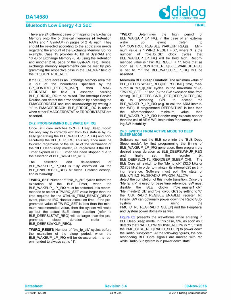
Datasheet Revision 3.4 09-Nov-2016
CFR0011-120-01 74 of 234 © 2014 Dialog Semiconductor
DA14580
Bluetooth Low Energy 4.2 SoC FINAL
There are 24 different cases of mapping the ExchangeMemory onto the 5 physical memories (4 RetentionRAMs and 1 SysRAM) in pages of 2 kB each. Theyshould be selected according to the application needsregarding the amount of the Exchange Memory. So, forexample, Case 15 provides 40 kB of SysRAM and10 kB of Exchange Memory (8 kB using the Retentionand another 2 kB page of the SysRAM cell). Hence,exchange memory requirements can be met by pro-gramming the respective case in the EM_MAP field ofthe GP_CONTROL_REG.
If the BLE core access an Exchange Memory area thatis out of the boundaries specified by theGP_CONTROL_REG[EM_MAP], then EMAC-CERRSTAT bit field is asserted, causingBLE_ERROR_IRQ to be raised. The Interrupt ServiceRoutine can detect the error condition by accessing theEMACCERRSTAT and can acknowledge by writing a“1” to EMACCERRACK. BLE_ERROR_IRQ is raisedwhen either EMACCERRSTAT or ERRORINTSTAT areasserted.
24.2 PROGRAMMING BLE WAKE UP IRQ
Once BLE core switches to “BLE Deep Sleep mode”the only way to correctly exit from this state is by ini-tially generating the BLE_WAKEUP_LP_IRQ and con-secutively the BLE_SLP_IRQ. This sequence must befollowed regardless of the cause of the termination ofthe “BLE Deep Sleep mode”, i.e. regardless if the BLETimer expired or BLE Timer has been stopped due tothe assertion of BLE_WAKEUP_REQ.
The assertion and de-assertion ofBLE_WAKEUP_LP_IRQ is fully controlled via theBLE_ENBPRESET_REG bit fields. Detailed descrip-tion is following:
TWIRQ_SET: Number of “ble_lp_clk” cycles before theexpiration of the BLE Timer, when theBLE_WAKEUP_LP_IRQ must be asserted. It is recom-mended to select a TWIRQ_SET value larger than thetime required for the XTAL16_TRIM_READY_DELAYevent, plus the IRQ Handler execution time. If the pro-grammed value of TWIRQ_SET is less than the mini-mum recommended value, then the system will wakeup but the actual BLE sleep duration (refer toBLE_DEEPSLSTAT_REG) will be larger than the pro-grammed sleep duration (refer toBLE_DEEPSLWKUP_REG).
TWIRQ_RESET: Number of “ble_lp_clk” cycles beforethe expiration of the sleep period, when theBLE_WAKEUP_LP_IRQ will be de-asserted. It is rec-ommended to always set to “1”.
TWEXT: Determines the high period ofBLE_WAKEUP_LP_IRQ, in the case of an externalwake up event (refer toGP_CONTROL_REG[BLE_WAKEUP_REQ]). Mini-mum value is "TWIRQ_RESET + X", where X is thenumber of “ble_lp_clk” clock cycles thatBLE_WAKEUP_LP_IRQ will be held high. Recom-mended value is "TWIRQ_RESET + 1". Note that assoon as GP_CONTROL_REG[BLE_WAKEUP_REQ]is set to “1” the BLE_WAKEUP_LP_IRQ will beasserted.
Minimum BLE Sleep Duration: The minimum value ofBLE_DEEPSLWKUP_REG[DEEPSLTIME] time, mea-sured in “ble_lp_clk” cycles, is the maximum of (a)“TWIRQ_SET + 1” and (b) the SW execution time fromsetting BLE_DEEPSLCNTL_REG[DEEP_SLEEP_ON]up to preparing CPU to accept theBLE_WAKEUP_LP_IRQ (e.g. to call the ARM instruc-tion WFI). If programmed DEEPSLTIME is less thanthe aforementioned minimum value, thenBLE_WAKEUP_LP_IRQ Handler may execute soonerthan the call of ARM WFI instruction for example, caus-ing SW instability.
24.3 SWITCH FROM ACTIVE MODE TO DEEP SLEEP MODE
Software can set the BLE core into the “BLE DeepSleep mode”, by first programming the timing ofBLE_WAKEUP_LP_IRQ generation, then program thedesired sleep duration at BLE_DEEPSLWKUP_REGand finally set the register bitBLE_DEEPSLCNTL_REG[DEEP_SLEEP_ON]. TheBLE Core will switch to the “ble_lp_clk” (32.0 kHz or32.768 kHz) in order to maintain its internal 625 s tim-ing reference. Software must poll the state ofBLE_CNTL2_REG[RADIO_PWRDN_ALLOW] todetect the completion of this mode transition. Once the“ble_lp_clk” is used for base time reference, SW mustdisable the BLE clocks (“ble_master1_clk”,“ble_master2_clk” and “ble_crypt_clk”) by setting to “0”the CLK_RADIO_REG[BLE_ENABLE] register bit.Finally, SW can optionally power down the Radio Sub-system by using thePMU_CTRL_REG[RADIO_SLEEP] and the Peripheraland System power domains as well.
Figure 62 presents the waveforms while entering inBLE Deep Sleep mode. In this case, SW, as soon as itdetects that RADIO_PWRDOWN_ALLOW is “1”, it setsthe PMU_CTRL_REG[RADIO_SLEEP] to power downthe Radio Subsystem. At the following figures, the cor-responding BLE Core signals are marked with redwhile Radio Subsystem is in power down state.

Datasheet Revision 3.4 09-Nov-2016
CFR0011-120-01 75 of 234 © 2014 Dialog Semiconductor
DA14580
Bluetooth Low Energy 4.2 SoC FINAL
24.4 SWITCH FROM DEEP SLEEP MODE TO ACTIVE MODE
There are two possibilities for BLE Core to terminatethe BLE Deep Sleep mode:
1. Termination at the end of a predetermined time.
2. Termination on software wake-up request, due to anexternal event.
24.4.1 Switching at Anchor Points
Figure 65 shows a typical deep sleep phase that is ter-minated at predetermined time. After a configurabletime before the scheduled wake up time (configuredvia BLE_ENBPRESET_REG register bit fields), theBLE Timer asserts the BLE_WAKEUP_LP_IRQ inorder to wake-up the CPU (powering up the SystemPower Domain). The BLE_WAKEUP_LP_IRQ InterruptHandler will prepare the code environment and theXTAL16M oscillator stabilization (refer toSYS_STAT_REG[XTAL16_SETTLED]) and will decidewhen the BLE Core will be ready to exit from the BLEDeep Sleep mode.
Once the SW decides that BLE Core can wake up, itmust enable the BLE clocks (viaCLK_RADIO_REG[BLE_ENABLE]) and power up theRadio Power Domain (refer toPMU_CTRL_REG[RADIO_SLEEP] andSYS_STAT_REG[RAD_IS_UP]).
After the expiration of the sleep period (as specified inBLE_DEEPSLWKUP_REG[DEEPSLTIME]) the BLETimer will not exit the BLE Deep Sleep mode until it willdetect that BLE Core is powered up. That means that ifthe SW requires more time to power up the BLE Core,then the final sleep duration (provided byBLE_DEEPSLSTAT_REG) will be larger than the pre-programmed value.
When BLE Timer is expired, BLE clocks are enabledand BLE Core (Radio Subsystem) is powered up, theBLE Core exists the “BLE Core Deep Sleep mode” andasserts the BLE_SLP_IRQ.
Figure 62 Entering into BLE Deep Sleep Mode
ble_lp_clk
ble_master1_gclken
ble_master1_clk
tick_625us_p
deepsltime[31:0] (hld)
deep_sleep_on
radio_pwrdown_allow
deepsldur[31:0]
0 N
0 1 2 3
Figure 63 Exit BLE Deep Sleep Mode at Predetermined Time (Zoom In)
ble_wakeup_lp_irq
ble_slp_irq
xtal16_settled
ble_enable
rad_is_up
ble_lp_clk
ble_master1_gclken
ble_master1_clk
deepsltime[31:0] (hld)
deepsldur[31:0]
finecnt[9:0]
N 0
N
twirq_reset=1
clk_status
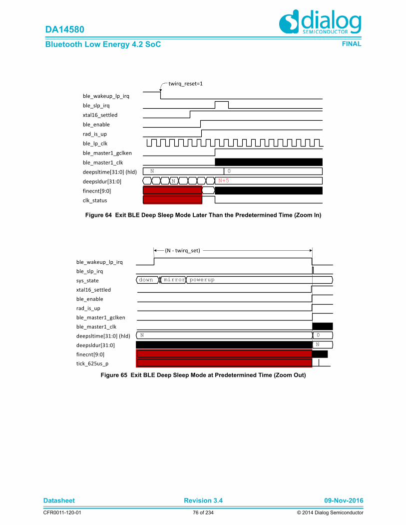
Datasheet Revision 3.4 09-Nov-2016
CFR0011-120-01 76 of 234 © 2014 Dialog Semiconductor
DA14580
Bluetooth Low Energy 4.2 SoC FINAL
Figure 64 Exit BLE Deep Sleep Mode Later Than the Predetermined Time (Zoom In)
ble_wakeup_lp_irq
ble_slp_irq
xtal16_settled
ble_enable
rad_is_up
ble_lp_clk
ble_master1_gclken
ble_master1_clk
deepsltime[31:0] (hld)
deepsldur[31:0]
finecnt[9:0]
N 0
N+5N
twirq_reset=1
clk_status
Figure 65 Exit BLE Deep Sleep Mode at Predetermined Time (Zoom Out)
ble_wakeup_lp_irq
ble_slp_irq
sys_state
xtal16_settled
ble_enable
rad_is_up
ble_master1_gclken
ble_master1_clk
deepsltime[31:0] (hld)
deepsldur[31:0]
finecnt[9:0]
tick_625us_p
mirror powerup
N 0
N
down
(N ‐ twirq_set)

Datasheet Revision 3.4 09-Nov-2016
CFR0011-120-01 77 of 234 © 2014 Dialog Semiconductor
DA14580
Bluetooth Low Energy 4.2 SoC FINAL
24.4.2 Switching Due to an External Event
Figure 66 shows a wake up from a deep sleep periodforced by the assertion of register bitGP_CONTROL_REG[BLE_WAKEUP_REQ].
Assume that the system is in Deep Sleep state, i.e. allPower Domains have been switched off, and both theWake-up Timer and Wake-up Controller have beenprogrammed appropriately. Then assume that an eventis detected at one of the GPIOs, causing the SystemPower Domain to wake-up due toWKUP_QUADDEC_IRQ. In that case, the SW willdecide to wake-up the BLE core, then it should set to
“1” the GP_CONTROL_REG[BLE_WAKEUP_REQ] inorder to force the wake up sequence.
In Figure 66 the BLE_WAKEUP_REQ is raised by thesoftware as soon as possible, causingBLE_WAKEUP_LP_IRQ Handler to be executed assoon as possible. It is also possible to raiseBLE_WAKEUP_REQ after the detection ofXTAL16_TRIM_READY, causing bothBLE_WAKEUP_LP_IRQ and BLE_SLP_IRQ Handlersto execute sequentially. The decision depends on thesoftware structure and the application.
As soon as bit field BLE_WAKEUP_REQ is set to “1”the BLE_WAKEUP_LP_IRQ will be asserted. In thatcase, the high period of BLE_WAKEUP_LP_IRQ iscontrolled via TWEXT. The recommended value ofTWEXT is "TWIRQ_RESET + 1", meaning thatBLE_WAKEUP_LP_IRQ will remain high for one“ble_llp_clk” period.
As long as the BLE_WAKEUP_REQ is high, enteringthe sleep mode is prohibited. Please note thatBLE_WAKEUP_REQ event can be disabled by settingBLE_DEEPSLCNTL_REG[EXTWKUPDSB].
Figure 66 Exit BLE Deep Sleep Mode Due to External Event
sys_state
xtal16_settled
rad_is_up
wakeup_irq
ble_wakeup_req
ble_wakeup_lp_irq
ble_slp_irq
deepsltime[31:0] (hld)
deepsldur[31:0]
finecnt[9:0]
tick_625us_p
down mirror powerup
N 0
K<N
twext=1

Datasheet Revision 3.4 09-Nov-2016
CFR0011-120-01 78 of 234 © 2014 Dialog Semiconductor
DA14580
Bluetooth Low Energy 4.2 SoC FINAL
25 RadioThe Radio Transceiver implements the RF part of theBluetooth low energy protocol. Together with the Blue-tooth 4.2 PHY layer, this provides a 93 dB RF link bud-get for reliable wireless communication.
All RF blocks are supplied by on-chip low-drop out-reg-ulators (LDOs). The bias scheme is programmable perblock and optimized for minimum power consumption.
The Bluetooth LE radio block diagram is given inFigure 67. It comprises the Receiver, Transmitter, Syn-thesizer, Rx/Tx combiner block, and Biasing LDOs.
Features
• Single ended RFIO interface, 50 matched
• Alignment free operation
• -93 dBm receiver sensitivity
• 0 dBm transmit output power
• Ultra low power consumption
• Fast frequency tuning minimizes overhead
25.1 RECEIVER
The RX frontend consists of a selective matching net-work, a low noise amplifier (LNA) and an image rejec-tion down conversion mixer. The LNA gain is controlledby the AGC.
The intermediate frequency (IF) part of the receivercomprises a complex filter and 2 variable gain amplifi-ers. This provides the necessary signal conditioningprior to digitalization. The digital demodulator block(DEM) provides a synchronous bit stream.
25.2 SYNTHESIZER
The RF Synthesizer generates the quadrature LO sig-nal for the mixer, but also generates the modulated TXoutput signal. The VCO runs at twice the required fre-quency and a dedicated divide-by-2 circuit generatesthe 2.4 GHz signals in the required phase relations. Itsfrequency is controlled by a classic 3rd order type IIPLL with a passive loop filter, operated in fractional-Nmode. The reference frequency is the 16 MHz crystalclock. The multi-modulus divider has a nominal divideratio of 153 which is varied by a modulator. Themodulation of the TX frequency is performed by 2-pointmodulation. The fractional divide ratio also contains theshaped TX data stream. A second modulation pathfeeds the TX data stream directly to the VCO. The lat-ter path is automatically calibrated from time to time toalign the low and high frequency parts of the 2-pointmodulation scheme.
25.3 TRANSMITTER
The RF power amplifier (RFPA) is an extremely effi-cient Class-D structure, providing typically 0 dBm to theantenna. It is fed by the VCO’s divide-by-2 circuit anddelivers its TX power to the antenna pin through thecombined RX/TX matching circuit.
25.4 RFIO
The RX/TX combiner block is a unique feature of theDA14580. It makes sure that the received power isapplied to the LNA with minimum losses towards theRFPA. In TX mode, the LNA poses a minimal load forthe RFPA and its input pins are protected from theRFPA. In both modes, the single ended RFIO port ismatched to 50 , in order to provide the simplest possi-ble interfacing to the antenna on the printed circuitboard.
25.5 BIASING
All RF blocks are supplied by on-chip low-drop out-reg-ulators (LDOs). The bias scheme is programmable perblock and optimized for minimum power consumption.
25.6 CONTROL
The radio control unit (RFCU) controls the block timingand configuration registers. The BLE interfaces directlywith the RFCU. The DA14580 can be put in test modeusing a standard Bluetooth tester (e.g.Rohde & Schwarz CBT with K57 option) by connectingthe antenna terminal for the RF link and the UART asdescribed in section 14.7.
Figure 67: Bluetooth Radio Block Diagram
SYNTH_CTRL
Rx
/Tx
LNA MIX IF ADC
SYNTH
PATESTMUX
Bias LDO
/N
RFIO
IFout
TEST[1:0]
DEM
RFCU
RFPA
LNA MIX IF ADC

Datasheet Revision 3.4 09-Nov-2016
CFR0011-120-01 79 of 234 © 2014 Dialog Semiconductor
DA14580
Bluetooth Low Energy 4.2 SoC FINAL
26 RegistersThis section contains a detailed view of the DA14580 registers. It is organized as follows: An overview table is pre-sented initially, which depicts all register names, addresses and descriptions. A detailed bit level description of eachregister follows.
The register file of the ARM Cortex-M0 can be found in the following documents, available on the ARM website:
Devices Generic User Guide:DUI0497A_cortex_m0_r0p0_generic_ug.pdf
Technical Reference Manual:DDI0432C_cortex_m0_r0p0_trm.pdf
These documents contain the register descriptions for the Nested Vectored Interrupt Controller (NVIC), the SystemControl Block (SCB) and the System Timer (SysTick).

Datasheet Revision 3.4 09-Nov-2016
CFR0011-120-01 80 of 234 © 2014 Dialog Semiconductor
DA14580
Bluetooth Low Energy 4.2 SoC FINAL
Table 26: Register Map
Address Port Description
0x40000000 BLE_RWBTLECNTL_REG BLE Control register
0x40000004 BLE_VERSION_REG Version register
0x40000008 BLE_RWBTLECONF_REG Configuration register
0x4000000C BLE_INTCNTL_REG Interrupt controller register
0x40000010 BLE_INTSTAT_REG Interrupt status register
0x40000014 BLE_INTRAWSTAT_REG Interrupt raw status register
0x40000018 BLE_INTACK_REG Interrupt acknowledge register
0x4000001C BLE_BASETIMECNT_REG Base time reference counter
0x40000020 BLE_FINETIMECNT_REG Fine time reference counter
0x40000024 BLE_BDADDRL_REG BLE device address LSB register
0x40000028 BLE_BDADDRU_REG BLE device address MSB register
0x4000002C BLE_CURRENTRXDESCPTR_REG Rx Descriptor Pointer for the Receive Buffer Chained List
0x40000030 BLE_DEEPSLCNTL_REG Deep-Sleep control register
0x40000034 BLE_DEEPSLWKUP_REG Time (measured in Low Power clock cycles) in Deep Sleep Mode before waking-up the device
0x40000038 BLE_DEEPSLSTAT_REG Duration of the last deep sleep phase register
0x4000003C BLE_ENBPRESET_REG Time in low power oscillator cycles register
0x40000040 BLE_FINECNTCORR_REG Phase correction value register
0x40000044 BLE_BASETIMECNTCORR_REG Base Time Counter
0x40000050 BLE_DIAGCNTL_REG Diagnostics Register
0x40000054 BLE_DIAGSTAT_REG Debug use only
0x40000058 BLE_DEBUGADDMAX_REG Upper limit for the memory zone
0x4000005C BLE_DEBUGADDMIN_REG Lower limit for the memory zone
0x40000060 BLE_ERRORTYPESTAT_REG Error Type Status registers
0x40000064 BLE_SWPROFILING_REG Software Profiling register
0x40000070 BLE_RADIOCNTL0_REG Radio interface control register
0x40000074 BLE_RADIOCNTL1_REG Radio interface control register
0x40000080 BLE_RADIOPWRUPDN_REG RX/TX power up/down phase register
0x40000090 BLE_ADVCHMAP_REG Advertising Channel Map
0x400000A0 BLE_ADVTIM_REG Advertising Packet Interval
0x400000A4 BLE_ACTSCANSTAT_REG Active scan register
0x400000B0 BLE_WLPUBADDPTR_REG Start address of public devices list
0x400000B4 BLE_WLPRIVADDPTR_REG Start address of private devices list
0x400000B8 BLE_WLNBDEV_REG Devices in white list
0x400000C0 BLE_AESCNTL_REG Start AES register
0x400000C4 BLE_AESKEY31_0_REG AES encryption key
0x400000C8 BLE_AESKEY63_32_REG AES encryption key
0x400000CC BLE_AESKEY95_64_REG AES encryption key
0x400000D0 BLE_AESKEY127_96_REG AES encryption key
0x400000D4 BLE_AESPTR_REG Pointer to the block to encrypt/decrypt
0x400000D8 BLE_TXMICVAL_REG AES / CCM plain MIC value
0x400000DC BLE_RXMICVAL_REG AES / CCM plain MIC value
0x400000E0 BLE_RFTESTCNTL_REG RF Testing Register

Datasheet Revision 3.4 09-Nov-2016
CFR0011-120-01 81 of 234 © 2014 Dialog Semiconductor
DA14580
Bluetooth Low Energy 4.2 SoC FINAL
0x400000F0 BLE_TIMGENCNTL_REG Timing Generator Register
0x400000F4 BLE_GROSSTIMTGT_REG Gross Timer Target value
0x400000F8 BLE_FINETIMTGT_REG Fine Timer Target value
0x400000FC BLE_SAMPLECLK_REG Samples the Base Time Counter
0x40000200 BLE_CNTL2_REG BLE Control Register 2
0x40000204 BLE_RF_DIAGIRQ_REG BLE/RF Diagnostic IRQ Control Register
0x40008000 OTPC_MODE_REG Mode register
0x40008004 OTPC_PCTRL_REG Bit-programming control register
0x40008008 OTPC_STAT_REG Status register
0x4000800C OTPC_AHBADR_REG AHB master start address
0x40008010 OTPC_CELADR_REG Macrocell start address
0x40008014 OTPC_NWORDS_REG Number of words
0x40008018 OTPC_FFPRT_REG Ports access to fifo logic
0x4000801C OTPC_FFRD_REG Latest read data from the OTPC_FFPRT_REG
0x50000000 CLK_AMBA_REG HCLK, PCLK, divider and clock gates
0x50000002 CLK_FREQ_TRIM_REG Xtal frequency trimming register
0x50000004 CLK_PER_REG Peripheral divider register
0x50000008 CLK_RADIO_REG Radio PLL control register
0x5000000A CLK_CTRL_REG Clock control register
0x50000010 PMU_CTRL_REG Power Management Unit control register
0x50000012 SYS_CTRL_REG System Control register
0x50000014 SYS_STAT_REG System status register
0x50000016 TRIM_CTRL_REG Control trimming of the XTAL16M
0x50000020 CLK_32K_REG 32 kHz oscillator register
0x50000022 CLK_16M_REG 16 MHz RC-oscillator register
0x50000024 CLK_RCX20K_REG 20 kHz RXC-oscillator control register
0x50000028 BANDGAP_REG Bandgap trimming
0x5000002A ANA_STATUS_REG Status bit of analog (power management) circuits
0x50000100 WKUP_CTRL_REG Control register for the wakeup counter
0x50000102 WKUP_COMPARE_REG Number of events before wakeup interrupt
0x50000104 WKUP_RESET_IRQ_REG Reset wakeup interrupt
0x50000106 WKUP_COUNTER_REG Actual number of events of the wakeup counter
0x50000108 WKUP_RESET_CNTR_REG Reset the event counter
0x5000010A WKUP_SELECT_P0_REG Select which inputs from P0 port can trigger wkup counter
0x5000010C WKUP_SELECT_P1_REG Select which inputs from P1 port can trigger wkup counter
0x5000010E WKUP_SELECT_P2_REG Select which inputs from P2 port can trigger wkup counter
0x50000110 WKUP_SELECT_P3_REG Select which inputs from P3 port can trigger wkup counter
0x50000112 WKUP_POL_P0_REG Select the sensitivity polarity for each P0 input
0x50000114 WKUP_POL_P1_REG Select the sensitivity polarity for each P1 input
0x50000116 WKUP_POL_P2_REG Select the sensitivity polarity for each P2 input
0x50000118 WKUP_POL_P3_REG Select the sensitivity polarity for each P3 input
Table 26: Register Map
Address Port Description

Datasheet Revision 3.4 09-Nov-2016
CFR0011-120-01 82 of 234 © 2014 Dialog Semiconductor
DA14580
Bluetooth Low Energy 4.2 SoC FINAL
0x50000200 QDEC_CTRL_REG Quad Decoder control register
0x50000202 QDEC_XCNT_REG Counter value of the X Axis
0x50000204 QDEC_YCNT_REG Counter value of the Y Axis
0x50000206 QDEC_CLOCKDIV_REG Clock divider register
0x50000208 QDEC_CTRL2_REG Quad Decoder control register
0x5000020A QDEC_ZCNT_REG Z_counter
0x50001000 UART_RBR_THR_DLL_REG Receive Buffer Register
0x50001004 UART_IER_DLH_REG Interrupt Enable Register
0x50001008 UART_IIR_FCR_REG Interrupt Identification Register/FIFO Control Register
0x5000100C UART_LCR_REG Line Control Register
0x50001010 UART_MCR_REG Modem Control Register
0x50001014 UART_LSR_REG Line Status Register
0x50001018 UART_MSR_REG Modem Status Register
0x5000101C UART_SCR_REG Scratchpad Register
0x50001020 UART_LPDLL_REG Low Power Divisor Latch Low
0x50001024 UART_LPDLH_REG Low Power Divisor Latch High
0x50001030 UART_SRBR_STHR0_REG Shadow Receive/Transmit Buffer Register
0x50001034 UART_SRBR_STHR1_REG Shadow Receive/Transmit Buffer Register
0x50001038 UART_SRBR_STHR2_REG Shadow Receive/Transmit Buffer Register
0x5000103C UART_SRBR_STHR3_REG Shadow Receive/Transmit Buffer Register
0x50001040 UART_SRBR_STHR4_REG Shadow Receive/Transmit Buffer Register
0x50001044 UART_SRBR_STHR5_REG Shadow Receive/Transmit Buffer Register
0x50001048 UART_SRBR_STHR6_REG Shadow Receive/Transmit Buffer Register
0x5000104C UART_SRBR_STHR7_REG Shadow Receive/Transmit Buffer Register
0x50001050 UART_SRBR_STHR8_REG Shadow Receive/Transmit Buffer Register
0x50001054 UART_SRBR_STHR9_REG Shadow Receive/Transmit Buffer Register
0x50001058 UART_SRBR_STHR10_REG Shadow Receive/Transmit Buffer Register
0x5000105C UART_SRBR_STHR11_REG Shadow Receive/Transmit Buffer Register
0x50001060 UART_SRBR_STHR12_REG Shadow Receive/Transmit Buffer Register
0x50001064 UART_SRBR_STHR13_REG Shadow Receive/Transmit Buffer Register
0x50001068 UART_SRBR_STHR14_REG Shadow Receive/Transmit Buffer Register
0x5000106C UART_SRBR_STHR15_REG Shadow Receive/Transmit Buffer Register
0x5000107C UART_USR_REG UART Status register.
0x50001080 UART_TFL_REG Transmit FIFO Level
0x50001084 UART_RFL_REG Receive FIFO Level.
0x50001088 UART_SRR_REG Software Reset Register.
0x5000108C UART_SRTS_REG Shadow Request to Send
0x50001090 UART_SBCR_REG Shadow Break Control Register
0x50001094 UART_SDMAM_REG Shadow DMA Mode
0x50001098 UART_SFE_REG Shadow FIFO Enable
0x5000109C UART_SRT_REG Shadow RCVR Trigger
0x500010A0 UART_STET_REG Shadow TX Empty Trigger
0x500010A4 UART_HTX_REG Halt TX
0x500010F4 UART_CPR_REG Component Parameter Register
Table 26: Register Map
Address Port Description

Datasheet Revision 3.4 09-Nov-2016
CFR0011-120-01 83 of 234 © 2014 Dialog Semiconductor
DA14580
Bluetooth Low Energy 4.2 SoC FINAL
0x500010F8 UART_UCV_REG Component Version
0x500010FC UART_CTR_REG Component Type Register
0x50001100 UART2_RBR_THR_DLL_REG Receive Buffer Register
0x50001104 UART2_IER_DLH_REG Interrupt Enable Register
0x50001108 UART2_IIR_FCR_REG Interrupt Identification Register/FIFO Control Register
0x5000110C UART2_LCR_REG Line Control Register
0x50001110 UART2_MCR_REG Modem Control Register
0x50001114 UART2_LSR_REG Line Status Register
0x50001118 UART2_MSR_REG Modem Status Register
0x5000111C UART2_SCR_REG Scratchpad Register
0x50001120 UART2_LPDLL_REG Low Power Divisor Latch Low
0x50001124 UART2_LPDLH_REG Low Power Divisor Latch High
0x50001130 UART2_SRBR_STHR0_REG Shadow Receive/Transmit Buffer Register
0x50001134 UART2_SRBR_STHR1_REG Shadow Receive/Transmit Buffer Register
0x50001138 UART2_SRBR_STHR2_REG Shadow Receive/Transmit Buffer Register
0x5000113C UART2_SRBR_STHR3_REG Shadow Receive/Transmit Buffer Register
0x50001140 UART2_SRBR_STHR4_REG Shadow Receive/Transmit Buffer Register
0x50001144 UART2_SRBR_STHR5_REG Shadow Receive/Transmit Buffer Register
0x50001148 UART2_SRBR_STHR6_REG Shadow Receive/Transmit Buffer Register
0x5000114C UART2_SRBR_STHR7_REG Shadow Receive/Transmit Buffer Register
0x50001150 UART2_SRBR_STHR8_REG Shadow Receive/Transmit Buffer Register
0x50001154 UART2_SRBR_STHR9_REG Shadow Receive/Transmit Buffer Register
0x50001158 UART2_SRBR_STHR10_REG Shadow Receive/Transmit Buffer Register
0x5000115C UART2_SRBR_STHR11_REG Shadow Receive/Transmit Buffer Register
0x50001160 UART2_SRBR_STHR12_REG Shadow Receive/Transmit Buffer Register
0x50001164 UART2_SRBR_STHR13_REG Shadow Receive/Transmit Buffer Register
0x50001168 UART2_SRBR_STHR14_REG Shadow Receive/Transmit Buffer Register
0x5000116C UART2_SRBR_STHR15_REG Shadow Receive/Transmit Buffer Register
0x5000117C UART2_USR_REG UART Status register.
0x50001180 UART2_TFL_REG Transmit FIFO Level
0x50001184 UART2_RFL_REG Receive FIFO Level.
0x50001188 UART2_SRR_REG Software Reset Register.
0x5000118C UART2_SRTS_REG Shadow Request to Send
0x50001190 UART2_SBCR_REG Shadow Break Control Register
0x50001194 UART2_SDMAM_REG Shadow DMA Mode
0x50001198 UART2_SFE_REG Shadow FIFO Enable
0x5000119C UART2_SRT_REG Shadow RCVR Trigger
0x500011A0 UART2_STET_REG Shadow TX Empty Trigger
0x500011A4 UART2_HTX_REG Halt TX
0x500011F4 UART2_CPR_REG Component Parameter Register
0x500011F8 UART2_UCV_REG Component Version
0x500011FC UART2_CTR_REG Component Type Register
0x50001200 SPI_CTRL_REG SPI control register 0
0x50001202 SPI_RX_TX_REG0 SPI RX/TX register0
Table 26: Register Map
Address Port Description

Datasheet Revision 3.4 09-Nov-2016
CFR0011-120-01 84 of 234 © 2014 Dialog Semiconductor
DA14580
Bluetooth Low Energy 4.2 SoC FINAL
0x50001204 SPI_RX_TX_REG1 SPI RX/TX register1
0x50001206 SPI_CLEAR_INT_REG SPI clear interrupt register
0x50001208 SPI_CTRL_REG1 SPI control register 1
0x50001300 I2C_CON_REG I2C Control Register
0x50001304 I2C_TAR_REG I2C Target Address Register
0x50001308 I2C_SAR_REG I2C Slave Address Register
0x50001310 I2C_DATA_CMD_REG I2C Rx/Tx Data Buffer and Command Register
0x50001314 I2C_SS_SCL_HCNT_REG Standard Speed I2C Clock SCL High Count Register
0x50001318 I2C_SS_SCL_LCNT_REG Standard Speed I2C Clock SCL Low Count Register
0x5000131C I2C_FS_SCL_HCNT_REG Fast Speed I2C Clock SCL High Count Register
0x50001320 I2C_FS_SCL_LCNT_REG Fast Speed I2C Clock SCL Low Count Register
0x5000132C I2C_INTR_STAT_REG I2C Interrupt Status Register
0x50001330 I2C_INTR_MASK_REG I2C Interrupt Mask Register
0x50001334 I2C_RAW_INTR_STAT_REG I2C Raw Interrupt Status Register
0x50001338 I2C_RX_TL_REG I2C Receive FIFO Threshold Register
0x5000133C I2C_TX_TL_REG I2C Transmit FIFO Threshold Register
0x50001340 I2C_CLR_INTR_REG Clear Combined and Individual Interrupt Register
0x50001344 I2C_CLR_RX_UNDER_REG Clear RX_UNDER Interrupt Register
0x50001348 I2C_CLR_RX_OVER_REG Clear RX_OVER Interrupt Register
0x5000134C I2C_CLR_TX_OVER_REG Clear TX_OVER Interrupt Register
0x50001350 I2C_CLR_RD_REQ_REG Clear RD_REQ Interrupt Register
0x50001354 I2C_CLR_TX_ABRT_REG Clear TX_ABRT Interrupt Register
0x50001358 I2C_CLR_RX_DONE_REG Clear RX_DONE Interrupt Register
0x5000135C I2C_CLR_ACTIVITY_REG Clear ACTIVITY Interrupt Register
0x50001360 I2C_CLR_STOP_DET_REG Clear STOP_DET Interrupt Register
0x50001364 I2C_CLR_START_DET_REG Clear START_DET Interrupt Register
0x50001368 I2C_CLR_GEN_CALL_REG Clear GEN_CALL Interrupt Register
0x5000136C I2C_ENABLE_REG I2C Enable Register
0x50001370 I2C_STATUS_REG I2C Status Register
0x50001374 I2C_TXFLR_REG I2C Transmit FIFO Level Register
0x50001378 I2C_RXFLR_REG I2C Receive FIFO Level Register
0x5000137C I2C_SDA_HOLD_REG I2C SDA Hold Time Length Register
0x50001380 I2C_TX_ABRT_SOURCE_REG I2C Transmit Abort Source Register
0x50001394 I2C_SDA_SETUP_REG I2C SDA Setup Register
0x50001398 I2C_ACK_GENERAL_CALL_REG I2C ACK General Call Register
0x5000139C I2C_ENABLE_STATUS_REG I2C Enable Status Register
0x500013A0 I2C_IC_FS_SPKLEN_REG I2C SS and FS spike suppression limit Size
0x50001400 GPIO_IRQ0_IN_SEL_REG GPIO interrupt selection for GPIO_IRQ0
0x50001402 GPIO_IRQ1_IN_SEL_REG GPIO interrupt selection for GPIO_IRQ1
0x50001404 GPIO_IRQ2_IN_SEL_REG GPIO interrupt selection for GPIO_IRQ2
0x50001406 GPIO_IRQ3_IN_SEL_REG GPIO interrupt selection for GPIO_IRQ3
0x50001408 GPIO_IRQ4_IN_SEL_REG GPIO interrupt selection for GPIO_IRQ4
0x5000140C GPIO_DEBOUNCE_REG debounce counter value for GPIO inputs
0x5000140E GPIO_RESET_IRQ_REG GPIO interrupt reset register
Table 26: Register Map
Address Port Description

Datasheet Revision 3.4 09-Nov-2016
CFR0011-120-01 85 of 234 © 2014 Dialog Semiconductor
DA14580
Bluetooth Low Energy 4.2 SoC FINAL
0x50001410 GPIO_INT_LEVEL_CTRL_REG high or low level select for GPIO interrupts
0x50001412 KBRD_IRQ_IN_SEL0_REG GPIO interrupt selection for KBRD_IRQ for P0
0x50001414 KBRD_IRQ_IN_SEL1_REG GPIO interrupt selection for KBRD_IRQ for P1 and P2
0x50001416 KBRD_IRQ_IN_SEL2_REG GPIO interrupt selection for KBRD_IRQ for P3
0x50001500 GP_ADC_CTRL_REG General Purpose ADC Control Register
0x50001502 GP_ADC_CTRL2_REG General Purpose ADC Second Control Register
0x50001504 GP_ADC_OFFP_REG General Purpose ADC Positive Offset Register
0x50001506 GP_ADC_OFFN_REG General Purpose ADC Negative Offset Register
0x50001508 GP_ADC_CLEAR_INT_REG General Purpose ADC Clear Interrupt Register
0x5000150A GP_ADC_RESULT_REG General Purpose ADC Result Register
0x5000150C GP_ADC_DELAY_REG General Purpose ADC Delay Register
0x5000150E GP_ADC_DELAY2_REG General Purpose ADC Second Delay Register
0x50001600 CLK_REF_SEL_REG Select clock for oscillator calibration
0x50001602 CLK_REF_CNT_REG Count value for oscillator calibration
0x50001604 CLK_REF_VAL_L_REG XTAL16M reference cycles, lower 16 bits
0x50001606 CLK_REF_VAL_H_REG XTAL16M reference cycles, upper 16 bits
0x50003000 P0_DATA_REG P0 Data input / output register
0x50003002 P0_SET_DATA_REG P0 Set port pins register
0x50003004 P0_RESET_DATA_REG P0 Reset port pins register
0x50003006 P00_MODE_REG P00 Mode Register
0x50003008 P01_MODE_REG P01 Mode Register
0x5000300A P02_MODE_REG P02 Mode Register
0x5000300C P03_MODE_REG P03 Mode Register
0x5000300E P04_MODE_REG P04 Mode Register
0x50003010 P05_MODE_REG P05 Mode Register
0x50003012 P06_MODE_REG P06 Mode Register
0x50003014 P07_MODE_REG P07 Mode Register
0x50003020 P1_DATA_REG P1 Data input / output register
0x50003022 P1_SET_DATA_REG P1 Set port pins register
0x50003024 P1_RESET_DATA_REG P1 Reset port pins register
0x50003026 P10_MODE_REG P10 Mode Register
0x50003028 P11_MODE_REG P11 Mode Register
0x5000302A P12_MODE_REG P12 Mode Register
0x5000302C P13_MODE_REG P13 Mode Register
0x5000302E P14_MODE_REG P14 Mode Register
0x50003030 P15_MODE_REG P15 Mode Register
0x50003040 P2_DATA_REG P2 Data input / output register
0x50003042 P2_SET_DATA_REG P2 Set port pins register
0x50003044 P2_RESET_DATA_REG P2 Reset port pins register
0x50003046 P20_MODE_REG P20 Mode Register
0x50003048 P21_MODE_REG P21 Mode Register
0x5000304A P22_MODE_REG P22 Mode Register
0x5000304C P23_MODE_REG P23 Mode Register
0x5000304E P24_MODE_REG P24 Mode Register
Table 26: Register Map
Address Port Description

Datasheet Revision 3.4 09-Nov-2016
CFR0011-120-01 86 of 234 © 2014 Dialog Semiconductor
DA14580
Bluetooth Low Energy 4.2 SoC FINAL
0x50003050 P25_MODE_REG P25 Mode Register
0x50003052 P26_MODE_REG P26 Mode Register
0x50003054 P27_MODE_REG P27 Mode Register
0x50003056 P28_MODE_REG P28 Mode Register
0x50003058 P29_MODE_REG P29 Mode Register
0x50003070 P01_PADPWR_CTRL_REG Ports 0 and 1 Output Power Control Register
0x50003072 P2_PADPWR_CTRL_REG Port 2 Output Power Control Register
0x50003074 P3_PADPWR_CTRL_REG Port 3 Output Power Control Register
0x50003080 P3_DATA_REG P3 Data input / output register
0x50003082 P3_SET_DATA_REG P3 Set port pins register
0x50003084 P3_RESET_DATA_REG P3 Reset port pins register
0x50003086 P30_MODE_REG P30 Mode Register
0x50003088 P31_MODE_REG P31 Mode Register
0x5000308A P32_MODE_REG P32 Mode Register
0x5000308C P33_MODE_REG P33 Mode Register
0x5000308E P34_MODE_REG P34 Mode Register
0x50003090 P35_MODE_REG P35 Mode Register
0x50003092 P36_MODE_REG P36 Mode Register
0x50003094 P37_MODE_REG P37 Mode Register
0x50003100 WATCHDOG_REG Watchdog timer register.
0x50003102 WATCHDOG_CTRL_REG Watchdog control register.
0x50003200 CHIP_ID1_REG Chip identification register 1.
0x50003201 CHIP_ID2_REG Chip identification register 2.
0x50003202 CHIP_ID3_REG Chip identification register 3.
0x50003203 CHIP_SWC_REG Software compatibility register.
0x50003204 CHIP_REVISION_REG Chip revision register.
0x50003300 SET_FREEZE_REG Controls freezing of various timers/counters.
0x50003302 RESET_FREEZE_REG Controls unfreezing of various timers/counters.
0x50003304 DEBUG_REG Various debug information register.
0x50003306 GP_STATUS_REG General purpose system status register.
0x50003308 GP_CONTROL_REG General purpose system control register.
0x50003400 TIMER0_CTRL_REG Timer0 control register
0x50003402 TIMER0_ON_REG Timer0 on control register
0x50003404 TIMER0_RELOAD_M_REG 16 bits reload value for Timer0
0x50003406 TIMER0_RELOAD_N_REG 16 bits reload value for Timer0
0x50003408 PWM2_DUTY_CYCLE Duty Cycle for PWM2
0x5000340A PWM3_DUTY_CYCLE Duty Cycle for PWM3
0x5000340C PWM4_DUTY_CYCLE Duty Cycle for PWM4
0x5000340E TRIPLE_PWM_FREQUENCY Frequency for PWM 2,3 and 4
0x50003410 TRIPLE_PWM_CTRL_REG PWM 2 3 4 Control
Table 26: Register Map
Address Port Description
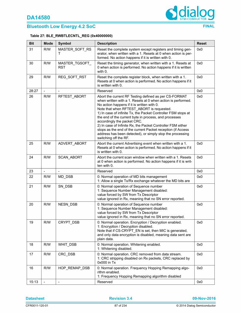
Datasheet Revision 3.4 09-Nov-2016
CFR0011-120-01 87 of 234 © 2014 Dialog Semiconductor
DA14580
Bluetooth Low Energy 4.2 SoC FINAL
Table 27: BLE_RWBTLECNTL_REG (0x40000000)
Bit Mode Symbol Description Reset
31 R/W MASTER_SOFT_RST
Reset the complete system except registers and timing gen-erator, when written with a 1. Resets at 0 when action is per-formed. No action happens if it is written with 0.
0x0
30 R/W MASTER_TGSOFT_RST
Reset the timing generator, when written with a 1. Resets at 0 when action is performed. No action happens if it is written with 0.
0x0
29 R/W REG_SOFT_RST Reset the complete register block, when written with a 1. Resets at 0 when action is performed. No action happens if it is written with 0.
0x0
28:27 - - Reserved 0x0
26 R/W RFTEST_ABORT Abort the current RF Testing defined as per CS-FORMAT when written with a 1. Resets at 0 when action is performed. No action happens if it is written with 0.Note that when RFTEST_ABORT is requested.1) In case of infinite Tx, the Packet Controller FSM stops at the end of the current byte in process, and processes accordingly the packet CRC.2) In case of Infinite Rx, the Packet Controller FSM either stops as the end of the current Packet reception (if Access address has been detected), or simply stop the processing switching off the RF.
0x0
25 R/W ADVERT_ABORT Abort the current Advertising event when written with a 1. Resets at 0 when action is performed. No action happens if it is written with 0.
0x0
24 R/W SCAN_ABORT Abort the current scan window when written with a 1. Resets at 0 when action is performed. No action happens if it is writ-ten with 0.
0x0
23 - - Reserved 0x0
22 R/W MD_DSB 0: Normal operation of MD bits management1: Allow a single Tx/Rx exchange whatever the MD bits are
0x0
21 R/W SN_DSB 0: Normal operation of Sequence number1: Sequence Number Management disabled:value forced by SW from Tx Descriptorvalue ignored in Rx, meaning that no SN error reported.
0x0
20 R/W NESN_DSB 0: Normal operation of Sequence number1: Sequence Number Management disabled:value forced by SW from Tx Descriptorvalue ignored in Rx, meaning that no SN error reported.
0x0
19 R/W CRYPT_DSB 0: Normal operation. Encryption / Decryption enabled.1: Encryption / Decryption disabled.Note that if CS-CRYPT_EN is set, then MIC is generated, and only data encryption is disabled, meaning data sent are plain data.
0x0
18 R/W WHIT_DSB 0: Normal operation. Whitening enabled.1: Whitening disabled.
0x0
17 R/W CRC_DSB 0: Normal operation. CRC removed from data stream.1: CRC stripping disabled on Rx packets, CRC replaced by 0x000 in Tx
0x0
16 R/W HOP_REMAP_DSB 0: Normal operation. Frequency Hopping Remapping algo-rithm enabled.1: Frequency Hopping Remapping algorithm disabled
0x0
15:13 - - Reserved 0x0
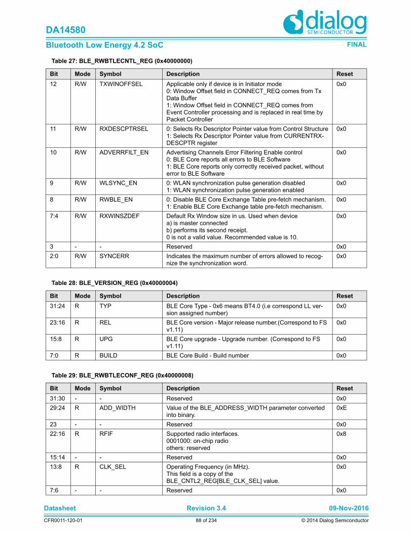
Datasheet Revision 3.4 09-Nov-2016
CFR0011-120-01 88 of 234 © 2014 Dialog Semiconductor
DA14580
Bluetooth Low Energy 4.2 SoC FINAL
12 R/W TXWINOFFSEL Applicable only if device is in Initiator mode0: Window Offset field in CONNECT_REQ comes from Tx Data Buffer1: Window Offset field in CONNECT_REQ comes from Event Controller processing and is replaced in real time by Packet Controller
0x0
11 R/W RXDESCPTRSEL 0: Selects Rx Descriptor Pointer value from Control Structure1: Selects Rx Descriptor Pointer value from CURRENTRX-DESCPTR register
0x0
10 R/W ADVERRFILT_EN Advertising Channels Error Filtering Enable control0: BLE Core reports all errors to BLE Software1: BLE Core reports only correctly received packet, without error to BLE Software
0x0
9 R/W WLSYNC_EN 0: WLAN synchronization pulse generation disabled1: WLAN synchronization pulse generation enabled
0x0
8 R/W RWBLE_EN 0: Disable BLE Core Exchange Table pre-fetch mechanism.1: Enable BLE Core Exchange table pre-fetch mechanism.
0x0
7:4 R/W RXWINSZDEF Default Rx Window size in us. Used when devicea) is master connectedb) performs its second receipt.0 is not a valid value. Recommended value is 10.
0x0
3 - - Reserved 0x0
2:0 R/W SYNCERR Indicates the maximum number of errors allowed to recog-nize the synchronization word.
0x0
Table 27: BLE_RWBTLECNTL_REG (0x40000000)
Bit Mode Symbol Description Reset
Table 28: BLE_VERSION_REG (0x40000004)
Bit Mode Symbol Description Reset
31:24 R TYP BLE Core Type - 0x6 means BT4.0 (i.e correspond LL ver-sion assigned number)
0x0
23:16 R REL BLE Core version - Major release number.(Correspond to FS v1.11)
0x0
15:8 R UPG BLE Core upgrade - Upgrade number. (Correspond to FS v1.11)
0x0
7:0 R BUILD BLE Core Build - Build number 0x0
Table 29: BLE_RWBTLECONF_REG (0x40000008)
Bit Mode Symbol Description Reset
31:30 - - Reserved 0x0
29:24 R ADD_WIDTH Value of the BLE_ADDRESS_WIDTH parameter converted into binary.
0xE
23 - - Reserved 0x0
22:16 R RFIF Supported radio interfaces.0001000: on-chip radioothers: reserved
0x8
15:14 - - Reserved 0x0
13:8 R CLK_SEL Operating Frequency (in MHz).This field is a copy of the BLE_CNTL2_REG[BLE_CLK_SEL] value.
0x0
7:6 - - Reserved 0x0

Datasheet Revision 3.4 09-Nov-2016
CFR0011-120-01 89 of 234 © 2014 Dialog Semiconductor
DA14580
Bluetooth Low Energy 4.2 SoC FINAL
5 R DMMODE 0: BLE Core is used as a standalone BLE device1: BLE Core is used in a Dual Mode device
0x0
4 R INTMODE 0: Interrupts are edge level generated, i.e pulse.1: Interrupts are trigger level generated, i.e stays active at 1 till acknowledgement
0x1
3 R WLAN 0: WLAN Coexistence mechanism not present1: WLAN Coexistence mechanism present
0x0
2 R USEDBG 0: Diagnostic port not instantiated1: Diagnostic port instantiated
0x1
1 R USECRYPT 0: Encryption block not present1: Encryption block present
0x1
0 R BUSWIDTH Processor bus width:0: 16 bits1: 32 bits
0x1
Table 29: BLE_RWBTLECONF_REG (0x40000008)
Bit Mode Symbol Description Reset
Table 30: BLE_INTCNTL_REG (0x4000000C)
Bit Mode Symbol Description Reset
31:16 R/W INTCSCNTL Selection of the CS counter that generates an interrupt. For example, if INTCNTL[3] is set, an interrupt is sent each time CS counter equals 3.
0xFF
15 R/W CSCNTDEVMSK CSCNT interrupt mask during event. This bit allows to enable CSCNT interrupt generation during events (i.e adver-tising, scanning, initiating, and connection)0: CSCNT Interrupt not generated during events.1: CSCNT Interrupt generated during events.
0x1
14:9 - - Reserved 0x0
8 R/W RADIOCNTLINTMSK Radio Controller interrupt mask0: Interrupt not generated1: Interrupt generated
0x0
7 R/W FINETGTIMINTMSK Fine Target Timer Mask0: Interrupt not generated1: Interrupt generated
0x0
6 R/W GROSSTGTIMINT-MSK
Gross Target Timer Mask0: Interrupt not generated1: Interrupt generated
0x0
5 R/W ERRORINTMSK Error Interrupt Mask0: Interrupt not generated1: Interrupt generated
0x0
4 R/W CRYPTINTMSK Encryption / Decryption Interrupt Mask0: Interrupt not generated1: Interrupt generated
0x1
3 R/W EVENTINTMSK End of event Interrupt Mask0: Interrupt not generated1: Interrupt generated
0x1
2 R/W SLPINTMSK Sleep Mode Interrupt Mask0: Interrupt not generated1: Interrupt generated
0x1
1 R/W RXINTMSK Rx Interrupt Mask0: Interrupt not generated1: Interrupt generated
0x1

Datasheet Revision 3.4 09-Nov-2016
CFR0011-120-01 90 of 234 © 2014 Dialog Semiconductor
DA14580
Bluetooth Low Energy 4.2 SoC FINAL
0 R/W CSCNTINTMSK 625usec Base Time Interrupt Mask0: Interrupt not generated1: Interrupt generated
0x1
Table 30: BLE_INTCNTL_REG (0x4000000C)
Bit Mode Symbol Description Reset
Table 31: BLE_INTSTAT_REG (0x40000010)
Bit Mode Symbol Description Reset
31:9 - - Reserved 0x0
8 R RADIOCNTLINT-STAT
Radio Controller interrupt status0: No Gross Target Timer interrupt.1: A Gross Target Timer interrupt is pending.
0x0
7 R FINETGTIMINTSTAT Masked Fine Target Timer Error interrupt status0: No Fine Target Timer interrupt.1: A Fine Target Timer interrupt is pending.
0x0
6 R GROSSTGTIMINT-STAT
Masked Gross Target Timer interrupt status0: No Gross Target Timer interrupt.1: A Gross Target Timer interrupt is pending.
0x0
5 R ERRORINTSTAT Masked Error interrupt status0: No Error interrupt.1: An Error interrupt is pending.
0x0
4 R CRYPTINTSTAT Masked Encryption/Decryption interrupt status0: No Encryption / Decryption interrupt.1: An Encryption / Decryption interrupt is pending.
0x0
3 R EVENTINTSTAT Masked End of Event interrupt status0: No End of Advertising / Scanning / Connection interrupt.1: An End of Advertising / Scanning / Connection interrupt is pending.
0x0
2 R SLPINTSTAT Masked Sleep interrupt status0: No End of Sleep Mode interrupt.1: An End of Sleep Mode interrupt is pending.
0x0
1 R RXINTSTAT Masked Packet Reception interrupt status0: No Rx interrupt.1: An Rx interrupt is pending.
0x0
0 R CSCNTINTSTAT Masked 625us base time reference interrupt status0: No 625us Base Time interrupt.1: A 625us Base Time interrupt is pending.
0x0
Table 32: BLE_INTRAWSTAT_REG (0x40000014)
Bit Mode Symbol Description Reset
31:9 - - Reserved 0x0
8 R RADIOCNTLIN-TRAWSTAT
Radio Controller interrupt raw status0: No Gross Target Timer interrupt.1: A Gross Target Timer interrupt is pending.
0x0
7 R FINETGTIMINTRAW-STAT
Fine Target Timer Error interrupt raw status0: No Fine Target Timer interrupt.1: A Fine Target Timer interrupt is pending.
0x0
6 R GROSSTGTIMIN-TRAWSTAT
Gross Target Timer interrupt raw status0: No Gross Target Timer interrupt.1: A Gross Target Timer interrupt is pending.
0x0

Datasheet Revision 3.4 09-Nov-2016
CFR0011-120-01 91 of 234 © 2014 Dialog Semiconductor
DA14580
Bluetooth Low Energy 4.2 SoC FINAL
5 R ERRORINTRAW-STAT
Error interrupt raw status0: No Error interrupt.1: An Error interrupt is pending.
0x0
4 R CRYPTINTRAWSTAT Encryption/Decryption interrupt raw status0: No Encryption / Decryption interrupt.1: An Encryption / Decryption interrupt is pending.
0x0
3 R EVENTINTRAWSTAT End of Event interrupt raw status0: No End of Advertising / Scanning / Connection interrupt.1: An End of Advertising / Scanning / Connection interrupt is pending.
0x0
2 R SLPINTRAWSTAT Sleep interrupt raw status0: No End of Sleep Mode interrupt.1: An End of Sleep Mode interrupt is pending.
0x0
1 R RXINTRAWSTAT Packet Reception interrupt raw status0: No Rx interrupt.1: An Rx interrupt is pending.
0x0
0 R CSCNTINTRAW-STAT
625us base time reference interrupt raw status0: No 625us Base Time interrupt.1: A 625us Base Time interrupt is pending.
0x0
Table 32: BLE_INTRAWSTAT_REG (0x40000014)
Bit Mode Symbol Description Reset
Table 33: BLE_INTACK_REG (0x40000018)
Bit Mode Symbol Description Reset
31:9 - - Reserved 0x0
8 W RADIOCNTLINTACK Radio Controller interrupt acknowledgement bitSoftware writing 1 acknowledges the Error interrupt. This bit resets RADIOCNTLINTSTAT and RADIOCNTLINTRAW-STAT flags.
0x0
7 W FINETGTIMINTACK Fine Target Timer interrupt acknowledgement bitSoftware writing 1 acknowledges the Error interrupt. This bit resets FINETGTIMINTSTAT and FINETGTIMINTRAWSTAT flags.
0x0
6 W GROSSTGTIMIN-TACK
Gross Target Timer interrupt acknowledgement bitSoftware writing 1 acknowledges the Error interrupt. This bit resets GROSSTGTIMINTSTAT and GROSSTGTIMIN-TRAWSTAT flags.
0x0
5 W ERRORINTACK Error interrupt acknowledgement bitSoftware writing 1 acknowledges the Error interrupt. This bit resets ERRORINTSTAT and ERRORINTRAWSTAT flags.
0x0
4 W CRYPTINTACK Encryption/Decryption interrupt acknowledgement bit Soft-ware writing 1 acknowledges the Encryption / Decryption interrupt. This bit resets CRYPTINTSTAT and CRYPTIN-TRAWSTAT flags.
0x0
3 W EVENTINTACK End of Event interrupt acknowledgment bitSoftware writing 1 acknowledges the End of Advertising / Scanning / Connection interrupt. This bit resets SLPINT-STAT and SLPINTRAWSTAT flags.
0x0
2 W SLPINTACK End of Deep Sleep interrupt acknowledgment bitSoftware writing 1 acknowledges the End of Sleep Mode interrupt. This bit resets SLPINTSTAT and SLPINTRAW-STAT flags.
0x0
1 W RXINTACK Packet Reception interrupt acknowledgment bitSoftware writing 1 acknowledges the Rx interrupt. This bit resets RXINTSTAT and RXINTRAWSTAT flags.
0x0

Datasheet Revision 3.4 09-Nov-2016
CFR0011-120-01 92 of 234 © 2014 Dialog Semiconductor
DA14580
Bluetooth Low Energy 4.2 SoC FINAL
0 W CSCNTINTACK 625us base time reference interrupt acknowledgment bitSoftware writing 1 acknowledges the CLKN interrupt. This bit resets CLKINTSTAT and CLKINTRAWSTAT flags.
0x0
Table 33: BLE_INTACK_REG (0x40000018)
Bit Mode Symbol Description Reset
Table 34: BLE_BASETIMECNT_REG (0x4000001C)
Bit Mode Symbol Description Reset
31:27 - - Reserved 0x0
26:0 R BASETIMECNT Value of the 625us base time reference counter. Updated each time BLE_SAMPLECLK_REG[SAMP] is written. Used by the SW in order to synchronize with the HW.
0x0
Table 35: BLE_FINETIMECNT_REG (0x40000020)
Bit Mode Symbol Description Reset
31:10 - - Reserved 0x0
9:0 R FINECNT Value of the current usec fine time reference counter. Updated each usec. Used by the SW in order to synchronize with the HW, and obtain a more precise sleep duration
0x0
Table 36: BLE_BDADDRL_REG (0x40000024)
Bit Mode Symbol Description Reset
31:0 R/W BDADDRL Bluetooth Low Energy Device Address. LSB part. 0x0
Table 37: BLE_BDADDRU_REG (0x40000028)
Bit Mode Symbol Description Reset
31:17 - - Reserved 0x0
16 R/W PRIV_NPUB Bluetooth Low Energy Device Address privacy indicator0: Public Bluetooth Device Address1: Private Bluetooth Device Address
0x0
15:0 R/W BDADDRU Bluetooth Low Energy Device Address. MSB part. 0x0
Table 38: BLE_CURRENTRXDESCPTR_REG (0x4000002C)
Bit Mode Symbol Description Reset
31:14 - - Reserved 0x0
13:0 R/W CURRENTRX-DESCPTR
Rx Descriptor Pointer that determines the starting point of the Receive Buffer Chained List.
0x0
Table 39: BLE_DEEPSLCNTL_REG (0x40000030)
Bit Mode Symbol Description Reset
31 R/W EXTWKUPDSB External Wake-Up disable0: BLE Core can be woken by external wake-up1: BLE Core cannot be woken up by external wake-up
0x0
30:16 - - Reserved 0x0

Datasheet Revision 3.4 09-Nov-2016
CFR0011-120-01 93 of 234 © 2014 Dialog Semiconductor
DA14580
Bluetooth Low Energy 4.2 SoC FINAL
15 R DEEP_SLEEP_STAT Indicator of current Deep Sleep clock mux status:0: BLE Core is not yet in Deep Sleep Mode1: BLE Core is in Deep Sleep Mode (only Low Power Clock is running)
0x0
14:5 - - Reserved 0x0
4 R/W SOFT_WAKEUP_REQ
Wake Up Request from BLE Software. Applies when system is in Deep Sleep Mode. It wakes up the BLE Core when writ-ten with a 1. Always read as 0. No action happens if it is writ-ten with 0.
0x0
3 R/W DEEP_SLEEP_CORR_EN
625us base time reference integer and fractional part correc-tion. Applies when system has been woken-up from Deep Sleep Mode. It enables Fine Counter and Base Time counter when written with a 1. Always read as 0. No action happens if it is written with 0.
0x0
2 R/W DEEP_SLEEP_ON 0: BLE Core in normal active mode1: Request BLE Core to switch in deep sleep mode.This bit is reset on DEEP_SLEEP_STAT falling edge.
0x0
1:0 R/W DEEP_SLEEP_IRQ_EN
Always set to "3" when DEEP_SLEEP_ON is set to "1".It controls the generation of BLE_WAKEUP_LP_IRQ.
0x0
Table 39: BLE_DEEPSLCNTL_REG (0x40000030)
Bit Mode Symbol Description Reset
Table 40: BLE_DEEPSLWKUP_REG (0x40000034)
Bit Mode Symbol Description Reset
31:0 R/W DEEPSLTIME Determines the time in Low Power Clock cycles to spend in Deep Sleep Mode before waking-up the device. This ensures a maximum of 37 hours and 16mn sleep mode capabilities at 32kHz. This ensures a maximum of 36 hours and 16mn sleep mode capabilities at 32.768kHz. If DEEPSL-TIME is set to zero, the Deep Sleep Time duration is consid-ered as infinite, and only wake up requests can restore active behaviorBLE Software must ensure DEEPSLTIME value to be greater than 2 in order to cope with control resynchronization requirements
0x0
Table 41: BLE_DEEPSLSTAT_REG (0x40000038)
Bit Mode Symbol Description Reset
31:0 R DEEPSLDUR Actual duration of the last deep sleep phase measured in Low Power Clock cycles. DEEPSLDUR is set to zero at the beginning of the deep sleep phase, and is incremented at each Low Power Clock cycle until the end of the deep sleep phase.
0x0
Table 42: BLE_ENBPRESET_REG (0x4000003C)
Bit Mode Symbol Description Reset
31:21 R/W TWEXT Minimum and recommended value is "TWIRQ_RESET + 1".In the case of wake-up due to an external wake-up request, TWEXT specifies the time delay in low power oscillator cycles to deassert BLE_WAKEUP_LP_IRQ.Refer also to GP_CONTROL_REG[BLE_WAKEUP_REQ].Range is [0...64 ms] for 32kHz; [0...62.5 ms] for 32.768kHz
0x0

Datasheet Revision 3.4 09-Nov-2016
CFR0011-120-01 94 of 234 © 2014 Dialog Semiconductor
DA14580
Bluetooth Low Energy 4.2 SoC FINAL
20:10 R/W TWIRQ_SET Minimum value is "TWIRQ_RESET + 1".Time in low power oscillator cycles to set BLE_WAKEUP_LP_IRQ before the BLE sleep timer expira-tion.Refer also to BLE_DEEPSLWKUP_REG[DEEPSLTIME].Range is [0...64 ms] for 32kHz; [0...62.5 ms] for 32.768kHz
0x0
9:0 R/W TWIRQ_RESET Recommended value is 1.Time in low power oscillator cycles to reset BLE_WAKEUP_LP_IRQ before the BLE sleep timer expira-tion.Refer also to BLE_DEEPSLWKUP_REG[DEEPSLTIME].Range is [0...32 ms] for 32kHz; [0...31.25 ms] for 32.768kHz.
0x0
Table 42: BLE_ENBPRESET_REG (0x4000003C)
Bit Mode Symbol Description Reset
Table 43: BLE_FINECNTCORR_REG (0x40000040)
Bit Mode Symbol Description Reset
31:10 - - Reserved 0x0
9:0 R/W FINECNTCORR Phase correction value for the 625usec reference counter (i.e Fine Counter) in us.
0x0
Table 44: BLE_BASETIMECNTCORR_REG (0x40000044)
Bit Mode Symbol Description Reset
31:27 - - Reserved 0x0
26:0 R/W BASETIMECNT-CORR
Base Time Counter correction value. 0x0
Table 45: BLE_DIAGCNTL_REG (0x40000050)
Bit Mode Symbol Description Reset
31 R/W DIAG3_EN 0: Disable diagnostic port 3 output. All outputs are set to 0.1: Enable diagnostic port 3 output.
0x0
30 - - Reserved 0x0
29:24 R/W DIAG3 Only relevant when DIAG3_EN = 1.Selection of the outputs that must be driven to the diagnostic port 3.
0x0
23 R/W DIAG2_EN 0: Disable diagnostic port 2 output. All outputs are set to 0.1: Enable diagnostic port 2 output.
0x0
22 - - Reserved 0x0
21:16 R/W DIAG2 Only relevant when DIAG2_EN = 1.Selection of the outputs that must be driven to the diagnostic port 2.
0x0
15 R/W DIAG1_EN 0: Disable diagnostic port 1 output. All outputs are set to 0.1: Enable diagnostic port 1 output.
0x0
14 - - Reserved 0x0
13:8 R/W DIAG1 Only relevant when DIAG1_EN = 1.Selection of the outputs that must be driven to the diagnostic port 1.
0x0
7 R/W DIAG0_EN 0: Disable diagnostic port 0 output. All outputs are set to 0.1: Enable diagnostic port 0 output.
0x0
6 - - Reserved 0x0
Datasheet Revision 3.4 09-Nov-2016
CFR0011-120-01 95 of 234 © 2014 Dialog Semiconductor
DA14580
Bluetooth Low Energy 4.2 SoC FINAL
5:0 R/W DIAG0 Only relevant when DIAG0_EN = 1.Selection of the outputs that must be driven to the diagnostic port 0.
0x0
Table 45: BLE_DIAGCNTL_REG (0x40000050)
Bit Mode Symbol Description Reset
Table 46: BLE_DIAGSTAT_REG (0x40000054)
Bit Mode Symbol Description Reset
31:24 R DIAG3STAT Directly connected to ble_dbg3[7:0] output. Debug use only. 0x0
23:16 R DIAG2STAT Directly connected to ble_dbg2[7:0] output. Debug use only. 0x0
15:8 R DIAG1STAT Directly connected to ble_dbg1[7:0] output. Debug use only. 0x0
7:0 R DIAG0STAT Directly connected to ble_dbg0[7:0] output. Debug use only. 0x0
Table 47: BLE_DEBUGADDMAX_REG (0x40000058)
Bit Mode Symbol Description Reset
31:16 - - Reserved 0x0
15:0 R/W ADDMAX Upper limit for the memory zone. 0x0
Table 48: BLE_DEBUGADDMIN_REG (0x4000005C)
Bit Mode Symbol Description Reset
31:16 - - Reserved 0x0
15:0 R/W ADDMIN Lower limit for the memory zone. 0x0
Table 49: BLE_ERRORTYPESTAT_REG (0x40000060)
Bit Mode Symbol Description Reset
31:12 - - Reserved 0x0
11 R CSFORMAT_ERROR
Indicates whether CS-FORMAT has been programmed with an invalid value: this is a major software programming fail-ure.0: No error1: Error occurred
0x0
10 R CSTXPTR_ERROR Indicates whether CS-TXPTR is null, this is a major software programming failure.0: No error1: Error occurred
0x0
9 - - Reserved 0x0
8 R RADIO_EMACC_ERROR
Radio Controller Exchange Memory access error, happens when Exchange Memory access are not served in time and data are corrupted.0: No error1: Error occurred
0x0
7 R LLCHMAP_ERROR Link Layer Channel Map error, happens when actual number of CS-LLCHMAP bit set to one is different from CS-NBCH-GOOD at the beginning of Frequency Hopping process0: No error1: Error occurred
0x0

Datasheet Revision 3.4 09-Nov-2016
CFR0011-120-01 96 of 234 © 2014 Dialog Semiconductor
DA14580
Bluetooth Low Energy 4.2 SoC FINAL
6 R IFS_UNDERRUN Inter Frame Space Under run, occurs if IFS time is not enough to update and read Control Structure/Descriptors, and/or White List parsing is not finished and/or Decryption time is too long to be finished on time0: No error1: Error occurred
0x0
5 R RXCRYPT_ERROR Real Time Decryption Error, happens when decryption is not finished before IFS time0: No error1: Error occurred
0x0
4 R WHITELIST_ERROR White List Timeout Error, occurs if White List parsing is not finished on time0: No error1: Error occurred
0x0
3 R APFM_ERROR Anticipated Pre-Fetch Mechanism error, happens when 3 consecutive Exchange Table entry have been programmed,0: no error1: Error occured
0x0
2 R TXDESC_ERROR Tx Descriptor Error, happens when fetched Tx Descriptor has TXDONE bit not set0: No error1: Error occurred
0x0
1 R PKTCNTL_EMACC_ERROR
Packet Controller Exchange Memory access error, happens when Exchange Memory access are not served in time and Tx/Rx data are corrupted0: No error1: Error occurred
0x0
0 R TXCRYPT_ERROR Real Time Encryption Error, happens when encryption is not finished before Tx Payload has to be sent0: No error1: Error occurred
0x0
Table 49: BLE_ERRORTYPESTAT_REG (0x40000060)
Bit Mode Symbol Description Reset
Table 50: BLE_SWPROFILING_REG (0x40000064)
Bit Mode Symbol Description Reset
31:0 R/W SWPROFVAL Software Profiling register: used by BLE Software for profil-ing purpose: this value is copied on Diagnostic port
0x0
Table 51: BLE_RADIOCNTL0_REG (0x40000070)
Bit Mode Symbol Description Reset
31:23 - - Reserved 0x0
22 R/W DPCORR_EN Enable the use of delayed DC compensated data path in Radio Correlator block1: Enable0: DisableMust be set to "0".
0x0
21:0 - - Reserved 0x2102
Table 52: BLE_RADIOCNTL1_REG (0x40000074)
Bit Mode Symbol Description Reset
31:21 - - Reserved 0x0

Datasheet Revision 3.4 09-Nov-2016
CFR0011-120-01 97 of 234 © 2014 Dialog Semiconductor
DA14580
Bluetooth Low Energy 4.2 SoC FINAL
20:16 R/W XRFSEL Extended radio selection field, Must be set to '00011'. 0x0
15:0 - - Reserved 0x0
Table 52: BLE_RADIOCNTL1_REG (0x40000074)
Bit Mode Symbol Description Reset
Table 53: BLE_RADIOPWRUPDN_REG (0x40000080)
Bit Mode Symbol Description Reset
31 - - Reserved 0x0
30:24 R/W RTRIP_DELAY Defines round trip delay value. This value correspond to the addition of data latency in Tx and data latency in Rx. Value is in us.
0x0
23:16 R/W RXPWRUP This register holds the length in us of the Rx power up phase for the current radio device. Default value is 210 us (reset value). Operating range depends of the selected radio.
0xD2
15:12 - - Reserved 0x0
11:8 R/W TXPWRDN This register extends the length in us of the Tx power down phase for the current radio device. Default value is 3us (reset value). Operating range depends of the selected radio.
0x3
7:0 R/W TXPWRUP This register holds the length in us of the Tx power up phase for the current radio device. Default value is 210 us (reset value). Operating range depends of the selected radio.
0xD2
Table 54: BLE_ADVCHMAP_REG (0x40000090)
Bit Mode Symbol Description Reset
31:3 - - Reserved 0x0
2:0 R/W ADVCHMAP Advertising Channel Map, defined as per the advertising connection settings. Contains advertising channels index 37 to 39. If ADVCHMAP[i] equals:0: Do not use data channel i+37.1: Use data channel i+37.
0x7
Table 55: BLE_ADVTIM_REG (0x400000A0)
Bit Mode Symbol Description Reset
31:14 - - Reserved 0x0
13:0 R/W ADVINT Advertising Packet Interval defines the time interval in between two ADV_xxx packet sent.Value is in usec.Value to program depends of the used Advertising Packet type and the device filtering policy. Please refer to Table 3-10 for details about ADVINT programming range.
0x0
Table 56: BLE_ACTSCANSTAT_REG (0x400000A4)
Bit Mode Symbol Description Reset
31:25 - - Reserved 0x0
24:16 R/W BACKOFF Active scan mode back-off counter initialization value. 0x0
15:9 - - Reserved 0x0
8:0 R/W UPPERLIMIT Active scan mode upper limit counter value. 0x0

Datasheet Revision 3.4 09-Nov-2016
CFR0011-120-01 98 of 234 © 2014 Dialog Semiconductor
DA14580
Bluetooth Low Energy 4.2 SoC FINAL
Table 57: BLE_WLPUBADDPTR_REG (0x400000B0)
Bit Mode Symbol Description Reset
31:16 - - Reserved 0x0
15:0 R/W WLPUBADDPTR Start address pointer of the public devices white list. 0x0
Table 58: BLE_WLPRIVADDPTR_REG (0x400000B4)
Bit Mode Symbol Description Reset
31:16 - - Reserved 0x0
15:0 R/W WLPRIVADDPTR Start address pointer of the private devices white list. 0x0
Table 59: BLE_WLNBDEV_REG (0x400000B8)
Bit Mode Symbol Description Reset
31:16 - - Reserved 0x0
15:8 R/W NBPRIVDEV Number of private devices in the white list. 0x0
7:0 R/W NBPUBDEV Number of public devices in the white list. 0x0
Table 60: BLE_AESCNTL_REG (0x400000C0)
Bit Mode Symbol Description Reset
31:30 - - Reserved 0x0
0 R/W AES_START Writing a 1 starts AES-128 ciphering process.This bit is reset once the process is finished (i.e BLE_CRYPT_IRQ interrupt occurs, even masked)
0x0
Table 61: BLE_AESKEY31_0_REG (0x400000C4)
Bit Mode Symbol Description Reset
31:0 R/W AESKEY31_0 AES encryption 128-bit key. Bit 31 down to 0 0x0
Table 62: BLE_AESKEY63_32_REG (0x400000C8)
Bit Mode Symbol Description Reset
31:0 R/W AESKEY63_32 AES encryption 128-bit key. Bit 63 down to 32 0x0
Table 63: BLE_AESKEY95_64_REG (0x400000CC)
Bit Mode Symbol Description Reset
31:0 R/W AESKEY95_64 AES encryption 128-bit key. Bit 95 down to 64 0x0
Table 64: BLE_AESKEY127_96_REG (0x400000D0)
Bit Mode Symbol Description Reset
31:0 R/W AESKEY127_96 AES encryption 128-bit key. Bit 127 down to 96 0x0
Table 65: BLE_AESPTR_REG (0x400000D4)
Bit Mode Symbol Description Reset
31:16 - - Reserved 0x0

Datasheet Revision 3.4 09-Nov-2016
CFR0011-120-01 99 of 234 © 2014 Dialog Semiconductor
DA14580
Bluetooth Low Energy 4.2 SoC FINAL
15:0 R/W AESPTR Pointer to the memory zone where the block to encrypt/decrypt is stored.
0x0
Table 65: BLE_AESPTR_REG (0x400000D4)
Bit Mode Symbol Description Reset
Table 66: BLE_TXMICVAL_REG (0x400000D8)
Bit Mode Symbol Description Reset
31:0 R TXMICVAL AES / CCM plain MIC value. Valid on BLE_CRYPT_IRQ interrupt (even masked)
0x0
Table 67: BLE_RXMICVAL_REG (0x400000DC)
Bit Mode Symbol Description Reset
31:0 R RXMICVAL AES / CCM plain MIC value. Valid on BLE_CRYPT_IRQ interrupt (even masked)
0x0
Table 68: BLE_RFTESTCNTL_REG (0x400000E0)
Bit Mode Symbol Description Reset
31 R/W INFINITERX Applicable for all frame format0: Normal mode of operation1: Infinite Rx window
0x0
30:16 - - Reserved 0x0
15 R/W INFINITETX Applicable for all frame format0: Normal mode of operation.1: Infinite Tx packet / Normal start of a packet but endless payloadIn case of infinite Tx payload, and when PRBS source is not selected, then RFTESTCNTL-TXLENGTH field provides the length of the pattern to repeat in the payload.
0x0
14 R/W TXLENGTHSRC Applicable only in Tx/Rx RF Test mode0: Normal mode of operation: TXDESC-TXADVLEN controls the Tx packet payload size1: Uses RFTESTCNTL-TXLENGTH packet length (can sup-port up to 512 bytes transmit)
0x0
13 R/W PRBSTYPE Applicable only in Tx/Rx RF Test mode0: Tx Packet Payload are PRBS9 type1: Tx Packet Payload are PRBS15 typePRBS9 is defined as p(x)=1+x5+x9. The LFSR used for the PRBS9 generator must be initialized with 0x1FF value.PRBS15 is defined as p(x)=1+x+x2+x12+x13+x14. The LFSR used for the PRBS15 generator must be initialized with 0x7FFF value.
0x0
12 R/W TXPLDSRC Applicable only in Tx/Rx RF Test mode0: Tx Packet Payload source is the Control Structure1: Tx Packet Payload are PRBS generator
0x0
11:9 - - Reserved 0x0
8:0 R/W TXLENGTH Applicable only in Tx/Rx RF Test modeTx packet length in number of byte
0x0

Datasheet Revision 3.4 09-Nov-2016
CFR0011-120-01 100 of 234 © 2014 Dialog Semiconductor
DA14580
Bluetooth Low Energy 4.2 SoC FINAL
Table 69: BLE_TIMGENCNTL_REG (0x400000F0)
Bit Mode Symbol Description Reset
31:8 - - Reserved 0x0
7:0 R/W PREFTECH_TIME Defines Exchange Table pre-fetch instant in us 0x0
Table 70: BLE_GROSSTIMTGT_REG (0x400000F4)
Bit Mode Symbol Description Reset
31:16 - - Reserved 0x0
15:0 R/W GROSSTARGET Gross Timer Target value on which a BLE_GROSSTGTIM_IRQ must be generated. This timer has a precision of 10ms: interrupt is generated only when GROSSTARGET[15:0] = BASETIMECNT[19:4] and BASE-TIMECNT[3:0] = 0.
0x0
Table 71: BLE_FINETIMTGT_REG (0x400000F8)
Bit Mode Symbol Description Reset
31:27 - - Reserved 0x0
26:0 R/W FINETARGET Fine Timer Target value on which a BLE_FINETGTIM_IRQ must be generated. This timer has a precision of 625us: interrupt is generated only when FINETARGET = BASE-TIMECNT
0x0
Table 72: BLE_SAMPLECLK_REG (0x400000FC)
Bit Mode Symbol Description Reset
31:30 - - Reserved 0x0
0 R/W SAMP Writing a 1 samples the Base Time Counter value in BASE-TIMECNT register. Resets at 0 when action is performed.
0x0
Table 73: BLE_CNTL2_REG (0x40000200)
Bit Mode Symbol Description Reset
31:22 - - Reserved 0x0
21 R/W BLE_RSSI_SEL 0: Select Peak-hold RSSI value (default).1: Select current Average RSSI value.
0x0
20 R WAKEUPLPSTAT The status of the BLE_WAKEUP_LP_IRQ. The Interrupt Service Routine of BLE_WAKEUP_LP_IRQ should return only when the WAKEUPLPSTAT is cleared.Note that BLE_WAKEUP_LP_IRQ is automatically acknowl-edged after the power up of the Radio Subsystem, plus one Low Power Clock period.
0x0
19 R/W SW_RPL_SPI Keep to 0. 0x0
18 R/W BB_ONLY Keep to 0. 0x0
17 R/W RADIO_ONLY Keep to 0. 0x0
16:15 - - Reserved 0x0

Datasheet Revision 3.4 09-Nov-2016
CFR0011-120-01 101 of 234 © 2014 Dialog Semiconductor
DA14580
Bluetooth Low Energy 4.2 SoC FINAL
14:9 R/W BLE_CLK_SEL BLE Clock Select.Specifies the BLE master clock absolute frequency in MHz.Typical values are 16 and 8.Value depends on the selected XTAL frequency and the value of CLK_RADIO_REG[BLE_DIV] bitfield. For example, if XTAL oscillates at 16MHz and CLK_RADIO_REG[BLE_DIV] = 1 (divide by 2), then BLE master clock frequency is 8MHz and BLE_CLK_SEL should be set to value 8.The selected BLE master clock frequency (affected by BLE_DIV and BLE_CLK_SEL) must be modified and set only during the initialization time, i.e. before setting BLE_RWBTLECNTL_REG[RWBLE_EN] to 1.Refer also to BLE_RWBTLECONF_REG[CLK_SEL].
0x0
8 R RADIO_PWRDN_ALLOW
This active high signal indicates when it is allowed for the BLE core (embedded in the Radio sub-System power domain) to be powered down.After the assertion of the BLE_DEEPSLCNTL_REG[DEEP_SLEEP_ON] a hardware sequence based on the Low Power clock will cause the assertion of RADIO_PWRDN_ALLOW. The RADIO_PWRDN_ALLOW will be cleared to "0" when the BLE core exits from the sleep state, i.e. when the BLE_SLP_IRQ will be asserted.
0x0
7 R/W MON_LP_CLK The SW can only write a "0" to this bit.Whenever a positive edge of the low power clock used by the BLE Timers is detected, then the HW will automatically set this bit to "1". This functionality will not work if BLE Timer is in reset state (refer to CLK_RADIO_REG[BLE_LP_RESET]).This bit can be used for SW synchronization, to debug the low power clock, etc.
0x0
6 R BLE_CLK_STAT 0: BLE uses low power clock1: BLE uses master clock
0x0
5 R/W DIAGPORT_REVERSE
BLE/RADIO Diagnostic Port Reverse order.
When this bit is "1", the mapping of the diagnostic bus DIAG-PORT[7:0] (controlled by DIAGPORT_SEL) to GPIOs (con-trolled by Pxy_MODE_REG[PID]) is reversed. The mapping is:
If "0" then DIAGPORT[7] is mapped to P0[7], etc.DIAGPORT[4] is mapped to P0[4],DIAGPORT[3] is mapped to P0[3] and P1[3], etc. andDIAGPORT[0] is mapped to P0[0] and P1[0].If "1" then DIAGPORT[7] is mapped to P0[0] and P1[0], etc.DIAGPORT[4] is mapped to P0[3] and P1[3],DIAGPORT[3] is mapped to P0[4], etc. andDIAGPORT[0] is mapped to P0[7].
0
Table 73: BLE_CNTL2_REG (0x40000200)
Bit Mode Symbol Description Reset

Datasheet Revision 3.4 09-Nov-2016
CFR0011-120-01 102 of 234 © 2014 Dialog Semiconductor
DA14580
Bluetooth Low Energy 4.2 SoC FINAL
4:3 R/W DIAGPORT_SEL BLE/RADIO Diagnostic Port Selection.
Controls the multiplexing of the internal diagnostic signals towards the 8-bit diagnostic bus DIAGPORT[7:0]. The DIAG-PORT[7:0] bit order may or may not be reversed by using the DIAGPORT_REVERSE bitfield and then it will be directed to the GPIOs P0[7:0] and P1[3:0]. (Note that the P1[3:0] diagnostic signals are the same with P0[3:0] signals.)
The DIAGPORT[7:0] value, depending on the DIAGPORT_SEL value, is:00: {BLE_DIAG2[7:5], BLE_DIAG1[4:3], BLE_DIAG0[2:0]}01: {BLE_DIAG2[7:5], BLE_DIAG1[4:3], BLE_DIAG0[2], wakeup_lp_irq, deep_sleep_stat_32k}10: RADIO_DIAG0[7:0]11: RADIO_DIAG1[7:0]
0x0
2 R/W EMACCERRMSK Exchange Memory Access Error Mask:When cleared to "0" the EM_ACC_ERR will not cause an BLE_ERROR_IRQ interrupt.When set to "1" an BLE_ERROR_IRQ will be generated as long as EM_ACC_ERR is "1".
0x1
1 W EMACCERRACK Exchange Memory Access Error Acknowledge.When the SW writes a "1" to this bit then the EMAC-CERRSTAT bit will be cleared.When the SW writes "0" it will have no affect.The read value is always "0".
0x0
0 R EMACCERRSTAT Exchange Memory Access Error Status:The bit is read-only and can be cleared only by writing a "1" at EMACCERRACK bitfield.This bit will be set to "1" by the hardware when the controller will access an EM page that is not mapped according to the EM_MAPPING value.When this bit is "1" then the BLE_ERROR_IRQ will be asserted as long as EMACCERRMSK is "1".
0x0
Table 73: BLE_CNTL2_REG (0x40000200)
Bit Mode Symbol Description Reset
Table 74: BLE_RF_DIAGIRQ_REG (0x40000204)
Bit Mode Symbol Description Reset
31 R DIAGIRQ_STAT_3 Same as DIAGIRQ_STAT_0. 0
30 R/W DIAGIRQ_EDGE_3 Same as DIAGIRQ_EDGE_0. 0
29:27 R/W DIAGIRQ_BSEL_3 Same as DIAGIRQ_BSEL_0. 0
26:25 R/W DIAGIRQ_WSEL_3 Same as DIAGIRQ_WSEL_0. 0
24 R/W DIAGIRQ_MASK_3 Same as DIAGIRQ_MASK_0. 0
23 R DIAGIRQ_STAT_2 Same as DIAGIRQ_STAT_0. 0
22 R/W DIAGIRQ_EDGE_2 Same as DIAGIRQ_EDGE_0. 0
21:19 R/W DIAGIRQ_BSEL_2 Same as DIAGIRQ_BSEL_0. 0
18:17 R/W DIAGIRQ_WSEL_2 Same as DIAGIRQ_WSEL_0. 0
16 R/W DIAGIRQ_MASK_2 Same as DIAGIRQ_MASK_0. 0
15 R DIAGIRQ_STAT_1 Same as DIAGIRQ_STAT_0. 0
14 R/W DIAGIRQ_EDGE_1 Same as DIAGIRQ_EDGE_0. 0
13:11 R/W DIAGIRQ_BSEL_1 Same as DIAGIRQ_BSEL_0. 0
10:9 R/W DIAGIRQ_WSEL_1 Same as DIAGIRQ_WSEL_0. 0
8 R/W DIAGIRQ_MASK_1 Same as DIAGIRQ_MASK_0. 0
Datasheet Revision 3.4 09-Nov-2016
CFR0011-120-01 103 of 234 © 2014 Dialog Semiconductor
DA14580
Bluetooth Low Energy 4.2 SoC FINAL
7 R DIAGIRQ_STAT_0 Diagnostic IRQ Status 0
This bit is read only. It is automatically cleared to "0" on each read of the BLE_RF_DIAGIRQ_REG register. It is automati-cally asserted to "1" on each detection of the selected edge, of the selected bit, of the selected word.
0
6 R/W DIAGIRQ_EDGE_0 Diagnostic IRQ Edge 0
Selects the edge of the selected bit (refer to DIAGIRQ_BSEL_0) that will trigger the assertion of DIAGIRQ_STAT_0.
If '0' then the positive edge is selected, when "1" the nega-tive edge is selected.
0
5:3 R/W DIAGIRQ_BSEL_0 Diagnostic IRQ Bit Select 0
Selects the bit of the 8-bit bus (as selected by the DIAGIRQ_WSEL_0) that will be used for the IRQ generation.
0
2:1 R/W DIAGIRQ_WSEL_0 Diagnostic IRQ Word Select 0
Selects the 8-bit diagnostic bus that will be used for the IRQ generation.
00: Selects the BLE_DIAG001: Selects the BLE_DIAG110: Selects the RADIO_DIAG011: Selects the RADIO_DIAG1
0
0 R/W DIAGIRQ_MASK_0 Diagnostic IRQ Mask 0
When set to "1" a BLE_RF_DIAG_IRQ will be generated on each rise of the DIAGIRQ_STAT_0 bit.
When cleared to "0" no IRQ will be generated.
0
Table 74: BLE_RF_DIAGIRQ_REG (0x40000204)
Bit Mode Symbol Description Reset
Table 75: OTPC_MODE_REG (0x40008000)
Bit Mode Symbol Description Reset
31:30 - - Reserved 0x0
29:28 R/W OTPC_MODE_PRG_PORT_MUX
Selects the source that is connected to the prg_port port of the controller.00 - {16'd0, BANDGAP_REG[15:0]}01 - {RF_RSSI_COMP_CTRL_REG[15:0], 8'd0, RFIO_CTRL1_REG{7:0]}10 - {3'd0, RF_LNA_CTRL3_REG[4:0], RF_LNA_CTRL2_REG[11:0], RF_LNA_CTRL1_REG[11:0]}11 - {28'd0, RF_VCO_CTRL_REG[3:0]}
See OTPC_MODE_PRG_PORT_SEL about the use of the prg_port
0x0
27:9 - - Reserved 0x0
8 R/W OPTC_MODE_PRG_FAST
Defines the timing that will be used for all the programming activities (APROG, MPROG and TWR)0 - Selects the normal timing1 - Selects the fast timing
0
Datasheet Revision 3.4 09-Nov-2016
CFR0011-120-01 104 of 234 © 2014 Dialog Semiconductor
DA14580
Bluetooth Low Energy 4.2 SoC FINAL
7 R/W OTPC_MODE_PRG_PORT_SEL
Selects an alternative data source for the programming of the OTP macrocells, when the controller is configured in APROG mode.0 - The fifo will be used as the data source. The fifo will be filled with a way defined by the register OTPC_MODE_USE_DMA. The number of words that will be programmed is defined by OTPC_NWORDS.1 - Only one word will programmed. The value of the word is contained in the prg_port port of the controller. The values of the registers OTPC_MODE_USE_DMA, OTPC_NWORDS and the contents of the FIFO will not be used.
0x0
6 R/W OTPC_MODE_TWO_CC_ACC
Defines the duration of each read from the OTP macrocells.0 - Reads 16 bits of data every one clock cycle.1 - Reads 16 bits of data every two clock cycles.
0x0
5 R/W OTPC_MODE_FIFO_FLUSH
Writing 1, removes any content from the FIFO. This bit returns automatically to 0.
0x0
4 R/W OTPC_MODE_USE_DMA
Selects the use of the dma, when the controller is configured in one of the modes: AREAD or APROG.0 - DMAis not used. The data should be transfered from/to controller through OTPC_FFPRT_REG1 - DMA is used. Data transfers from/to controller are per-formed automatically. The AHB base address should be con-figured in OTPC_AHBADR_REG before the selection of the mode.If programming of the OTPC_MODE_REG is performed through the serial interface,the OTPC_MODE_USE_DMA will be set to 0 automatically.If the controller is in APROG mode and the OTPC_MODE_PRG_PORT_SEL is enabled, the dma will stay inactive.
0x0
3 - - Reserved 0x0
2:0 R/W OTPC_MODE_MODE
Defines the mode of operation of the OTPC controller. The encoding of the modes is as follows:000 - STBY mode001 - MREAD mode010 - MPROG mode011 - AREAD mode100 - APROG mode101 - Test mode. Reserved110 - Test mode. Reserved111 - Test mode. ReservedTo manually move between modes, always return to STBY mode first.
0x0
Table 75: OTPC_MODE_REG (0x40008000)
Bit Mode Symbol Description Reset
Table 76: OTPC_PCTRL_REG (0x40008004)
Bit Mode Symbol Description Reset
31:28 - - Reserved 0x0
27 R/W OTPC_PCTRL_ENU Enables the programming in the upper bank of the OTP.0 - Programming sequence is not applied in the upper bank.1 - Programming sequence is applied in the upper bank.
0x0
26 R/W OTPC_PCTRL_BITU Defines the value of the selected bit in the upper bank, after the programming sequence.
0x0

Datasheet Revision 3.4 09-Nov-2016
CFR0011-120-01 105 of 234 © 2014 Dialog Semiconductor
DA14580
Bluetooth Low Energy 4.2 SoC FINAL
25 R/W OTPC_PCTRL_ENL Enables the programming in the lower bank.0 - The programming sequence is not applied in the lower bank.1 -The programming sequence is applied in the lower bank.
0x0
24 R/W OTPC_PCTRL_BITL Defines the value of the selected bit in the lower bank, after the programming sequence.
0x0
23 R/W OTPC_PCTRL_BSELU
Selects between the U1 and U0 byte for the programming sequence in the upper bank.0 - Program the U0 byte1 - Program the U1 byte
0x0
22:20 R/W OTPC_PCTRL_BADRU
Selects the bit inside the Ux (x=0,1) byte, which will be pro-grammed in the upper bank.
0x0
19 R/W OTPC_PCTRL_BSELL
Selects between the L1 and L0 byte for the programming sequence in the lower bank.0 - Program the L0 byte1 - Program the L1 byte
0x0
18:16 R/W OTPC_PCTRL_BADRL
Selects the bit inside the Lx (x=0,1) byte, which will be pro-grammed in the lower bank.
0x0
15:13 - - Reserved 0x0
12:0 R/W OTPC_PCTRL_WADDR
Defines the address of a 32 bits word {U1,L1,U0,L0} in the macrocells, where one or two bits will be programmed. There are two macrocell banks, with 8 bits each. Each bank contribute with two memory positions for each 32 bits word. The Ux, Lx represent the bytes of the upper and lower bank respectively.
0x0
Table 76: OTPC_PCTRL_REG (0x40008004)
Bit Mode Symbol Description Reset
Table 77: OTPC_STAT_REG (0x40008008)
Bit Mode Symbol Description Reset
31:29 - - Reserved 0x0
28:16 R OTPC_STAT_NWORDS
Contains the current value of the words to be processed. 0
15 R OTPC_STAT_TERR_U
Indicates the upper bank as the source of a test error. This value is valid when OTPC_STAT_TERROR is valid.0 - There is no test error in the upper bank1 - A test error has occured in the upper bank
0x0
14 R OTPC_STAT_TERR_L
Indicates the lower bank as the source of a test error. The value is valid when OTPC_STAT_TERROR is valid.0 - There is no test error in the lower bank1 - A test error has occured in the lower bank
0x0
13 R OTPC_STAT_PERR_U
Indicates the upper bank as the source of a programming error. The value is valid when OTPC_STAT_PERROR is valid.0 - There is no programming error in the upper bank1 - A programming error has occured in the upper bank
0x0
12 R OTPC_STAT_PERR_L
Indicates the lower bank as the source of a programming error. The value is valid when OTPC_STAT_PERROR is valid.0 - There is no programming error in the lower bank1 - A programming error has occured in the lower bank
0x0
11:8 R OTPC_STAT_FWORDS
Indicates the number of words which contained in the fifo of the controller.
0x0
7:5 - - Reserved 0x0

Datasheet Revision 3.4 09-Nov-2016
CFR0011-120-01 106 of 234 © 2014 Dialog Semiconductor
DA14580
Bluetooth Low Energy 4.2 SoC FINAL
4 R OTPC_STAT_ARDY Monitors the progress of read or programming operations while in the AREAD or APROG modes.0 - The controller is busy while reading or programming (AREAD or APROG modes).1 - The controller is not busy in AREAD or APROG mode.
0x1
3 R OTPC_STAT_TERROR
Indicates the result of a test sequence. Should be checked after the end of a TBLANK, TDEC and TWR mode (OTPC_STAT_TRDY= 1).0 - The test sequence ends with no error.1 - The test sequence has failed.
0x0
2 R OTPC_STAT_TRDY Indicates the state of a test mode. Should be used to monitor the progress of the TBLANK, TDEC and TWR modes.0 - The controller is busy. A test mode is in progress.1 - There is no active test mode.
0x1
1 R OTPC_STAT_PERROR
Indicates that an error has occurred during the bit-program-ming process.0 - No error during the bit-programming process.1 - The process of bit-programming failed.When the controller is in MPROG mode, this bit should be checked after the end of the programming process (OTPC_STAT_PRDY= 1).During APROG mode, the value of this field is normal to change periodically. Upon finishing the operation in the APROG mode (OTPC_STAT_ARDY= 1), this field indicates if the programming has failed or ended succesfully.
0x0
0 R OTPC_STAT_PRDY Indicates the state of a bit-programming process.0 - The controller is busy. A bit-programming is in progress1 - The logic which performs bit-programming is idle.When the controller is in MPROG mode, this bit should be used to monitor the progress of a programming request.During APROG mode, the value of this field it is normal to changing periodically.
0x1
Table 77: OTPC_STAT_REG (0x40008008)
Bit Mode Symbol Description Reset
Table 78: OTPC_AHBADR_REG (0x4000800C)
Bit Mode Symbol Description Reset
31:2 R/W OTPC_AHBADR Tthe AHB address used by the AHB master interface of the controller (bits [31:2]).
0x0
1:0 - - Reserved 0x0
Table 79: OTPC_CELADR_REG (0x40008010)
Bit Mode Symbol Description Reset
31:13 - - Reserved 0x0
12:0 R/W OTPC_CELADR Defines a word address inside the macrocell. Used in modes AREAD and APROG and is automatically updated.
0x0
Table 80: OTPC_NWORDS_REG (0x40008014)
Bit Mode Symbol Description Reset
31:13 - - Reserved 0x0

Datasheet Revision 3.4 09-Nov-2016
CFR0011-120-01 107 of 234 © 2014 Dialog Semiconductor
DA14580
Bluetooth Low Energy 4.2 SoC FINAL
12:0 R/W OTPC_NWORDS The number of words (minus one) for reading/programming during the AREAD/APROG mode.If in APROG mode, and the OTPC_MODE_PRG_PORT_SEL is enabled (=1), this regis-ter will not be used and will stay unchanged.During mirroring, this register reflects the current amount of data that will be copied. It keeps its value until be written by the software with a new value. The number of the words that remaining to be processed by the controller is contained in the field OTPC_STAT_NWORDS.
0x0
Table 80: OTPC_NWORDS_REG (0x40008014)
Bit Mode Symbol Description Reset
Table 81: OTPC_FFPRT_REG (0x40008018)
Bit Mode Symbol Description Reset
31:0 R/W OTPC_FFPRT Provides access to the fifo through an access port. Write this register with the corresponding data, when the APROG mode is selected and the DMA is disabled. Read from this register the corresponding data, when the AREAD mode is selected and the DMA is disabled.Check OTPC_STAT_FWORDS register for data/space avail-ability, before accessing the fifo.
0x0
Table 82: OTPC_FFRD_REG (0x4000801C)
Bit Mode Symbol Description Reset
31:0 R OTPC_FFRD Contains the value read from the fifo, after a read of the OTPC_FFPRT_REG register.
0x0
Table 83: CLK_AMBA_REG (0x50000000)
Bit Mode Symbol Description Reset
15:8 - - Reserved 0x0
7 R/W OTP_ENABLE Clock enable for OTP controller 0x0
6 - - Reserved 0x0
5:4 R/W PCLK_DIV APB interface clock (PCLK). Divider is cascaded with HCLK_DIV. PCLK is HCLK divided by:0x0: divide by 10x1: divide by 20x2: divide by 40x3: divide by 8
0x2
3:2 - - Reserved 0x0
1:0 R/W HCLK_DIV AHB interface and microprocessor clock (HCLK). HCLK is source clock divided by:0x0: divide by 10x1: divide by 20x2: divide by 40x3: divide by 8
0x2
Table 84: CLK_FREQ_TRIM_REG (0x50000002)
Bit Mode Symbol Description Reset
15:11 - - Reserved 0x0

Datasheet Revision 3.4 09-Nov-2016
CFR0011-120-01 108 of 234 © 2014 Dialog Semiconductor
DA14580
Bluetooth Low Energy 4.2 SoC FINAL
10:8 R/W COARSE_ADJ Xtal frequency course trimming register.0x0: lowest frequency0x7: highest frequencyIncrement or decrement the binary value with 1. Wait approximately 200 us to allow the adjust-ment to settle.
0x0
7:0 R/W FINE_ADJ Xtal frequency fine trimming register.0x00: lowest frequency0xFF: highest frequency
0x0
Table 84: CLK_FREQ_TRIM_REG (0x50000002)
Bit Mode Symbol Description Reset
Table 85: CLK_PER_REG (0x50000004)
Bit Mode Symbol Description Reset
15 R/W QUAD_ENABLE Enable the Quadrature clock 0x0
14:12 - - Reserved 0x0
11 R/W SPI_ENABLE Enable SPI clock 0x0
10 - - Reserved 0x0
9:8 R/W SPI_DIV Division factor for SPI0x0: divide by 10x1: divide by 20x2: divide by 40x3: divide by 8
0x0
7 R/W UART1_ENABLE Enable UART1 clock 0x0
6 R/W UART2_ENABLE Enable UART2 clock 0x0
5 R/W I2C_ENABLE Enable I2C clock 0x0
4 R/W WAKEUPCT_ENABLE
Enable Wakeup CaptureTimer clock 0x0
3 R/W TMR_ENABLE Enable TIMER0 and TIMER2 clock 0x0
2 - - Reserved 0x0
1:0 R/W TMR_DIV Division factor for TIMER00x0: divide by 10x1: divide by 20x2: divide by 40x3: divide by 8
0x0
Table 86: CLK_RADIO_REG (0x50000008)
Bit Mode Symbol Description Reset
15:8 - - Reserved 0x0
7 R/W BLE_ENABLE Enable the BLE core clocks 0x0
6 R/W BLE_LP_RESET Reset for the BLE LP timer 0x1
5:4 R/W BLE_DIV Division factor for BLE core blocks0x0: divide by 10x1: divide by 20x2: divide by 40x3: divide by 8The programmed frequency should not be lower than 8 MHz and not faster than the programmed CPU clock frequency. Refer also to BLE_CNTL2_REG[BLE_CLK_SEL].
0x0
3 R/W RFCU_ENABLE Enable the RF control Unit clock 0x0
2 - - Reserved 0x0

Datasheet Revision 3.4 09-Nov-2016
CFR0011-120-01 109 of 234 © 2014 Dialog Semiconductor
DA14580
Bluetooth Low Energy 4.2 SoC FINAL
1:0 R/W RFCU_DIV Division factor for RF Control Unit0x0: divide by 10x1: divide by 20x2: divide by 40x3: divide by 8The programmed frequency must be exactly 8 MHz.
0x0
Table 86: CLK_RADIO_REG (0x50000008)
Bit Mode Symbol Description Reset
Table 87: CLK_CTRL_REG (0x5000000A)
Bit Mode Symbol Description Reset
15:8 - - Reserved 0x0
7 R RUNNING_AT_XTAL16M
Indicates that the XTAL16M clock is used as clock, and may not be switched off
0x1
6 R RUNNING_AT_RC16M
Indicates that the RC16M clock is used as clock 0x0
5 R RUNNING_AT_32K Indicates that either the RC32k or XTAL32k is being used as clock
0x0
4 - - Reserved 0x0
3 R/W XTAL16M_SPIKE_FLT_DISABLE
Disable spikefilter in digital clock 0x0
2 R/W XTAL16M_DISABLE Setting this bit instantaneously disables the 16 MHz crystal oscillator. Also, after sleep/wakeup cycle, the oscillator will not be enabled. This bit may not be set to '1'when "RUNNING_AT_XTAL16M is '1' to prevent deadlock. After resetting this bit, wait for XTAL16_SETTLED or XTAL16_TRIM_READY to become '1' before switching to XTAL16 clock source.
0x0
1:0 R/W SYS_CLK_SEL Selects the clock source.0x0: XTAL16M (check the XTAL16_SETTLED and XTAL16_TRIM_READY bits!!)0x1: RC16M0x2/0x3: either RC32k or XTAL32k is used
0x0
Table 88: PMU_CTRL_REG (0x50000010)
Bit Mode Symbol Description Reset
15:12 - - Reserved 0x0
11:8 R/W RETENTION_MODE Select the retainability of the 4 retention RAM macros.'1' is retainable, '0' is power gated.(3) is RETRAM4(2) is RETRAM3(1) is RETRAM2(0) is RETRAM1
0x0
7 R/W FORCE_BOOST Force the DCDC into boost mode at next wakeup.Setting this bit reduces the deepsleep current.FORCE_BOOST has highest priority.When either FORCE_BOOST or FORCE_BUCK have been written, these bits cannot be changed.
0x0
6 R/W FORCE_BUCK Force the DCDC into buck mode at next wakeup.Setting this bit reduces the deepsleep current.FORCE_BOOST has highest priority.When either FORCE_BOOST or FORCE_BUCK have been written, these bits cannot be changed.
0x0
Datasheet Revision 3.4 09-Nov-2016
CFR0011-120-01 110 of 234 © 2014 Dialog Semiconductor
DA14580
Bluetooth Low Energy 4.2 SoC FINAL
5:4 R/W OTP_COPY_DIV Sets the HCLK division during OTP mirroring 0x0
2 R/W RADIO_SLEEP Put the digital part of the radio in powerdown 0x1
1 R/W PERIPH_SLEEP Put all peripherals (I2C, UART, SPI, ADC) in powerdown 0x1
0 R/W RESET_ON_WAKEUP
Perform a Hardware Reset after waking up. Booter will be started.
0x0
Table 88: PMU_CTRL_REG (0x50000010)
Bit Mode Symbol Description Reset
Table 89: SYS_CTRL_REG (0x50000012)
Bit Mode Symbol Description Reset
15 W SW_RESET Writing a '1' to this bit will reset the device, except for:SYS_CTRL_REGCLK_FREQ_TRIM_REG...
0x0
9 R/W TIMEOUT_DISABLE Disables timeout in Power statemachine. By default, the statemachine continues if after 2 ms the blocks are not started up. This can be read back fromANA_STATUS_REG.
0x0
8 - - Reserved 0x0
7 R/W DEBUGGER_ENABLE
Enable the debugger. This bit is set by the booter according to the OTP header. If not set, the SWDIO and SW_CLK can be used as gpio ports.
0x0
6 R/W OTPC_RESET_REQ Reset request for the OTP controller. 0x0
5 R/W PAD_LATCH_EN Latches the control signals of the pads for state retention in powerdown mode.0: Control signals are retained1: Latch is transparant, pad can be recontrolled
0x1
4 R/W OTP_COPY Enables OTP to SysRAM copy action after waking up PD_SYS
0x0
3 R/W CLK32_SOURCE Sets the clock source of the 32 kHz clock0 = RC-oscillator1 = 32 kHz crystal oscillator
0x0
2 R/W RET_SYSRAM Sets the development phase mode.The PD_SYS is not actually power gated (SysRAM is retained).No copy action to SysRAM is done when the system wakes up.For emulating startup time, the OTP_COPY bit still needs to be set.
0x0
1:0 R/W REMAP_ADR0 Controls which memory is located at address 0x0000 for execution.0x0: ROM0x1: OTP0x2: SysRAM0x3: RetRAM
0x0
Table 90: SYS_STAT_REG (0x50000014)
Bit Mode Symbol Description Reset
15:8 - - Reserved 0x0
7 R XTAL16_SETTLED Indicates that XTAL16 has had > 2 ms of settle time 0x0
6 R XTAL16_TRIM_READY
Indicates that XTAL trimming mechanism is ready, i.e. the trimming equals CLK_FREQ_TRIM_REG.
0x1

Datasheet Revision 3.4 09-Nov-2016
CFR0011-120-01 111 of 234 © 2014 Dialog Semiconductor
DA14580
Bluetooth Low Energy 4.2 SoC FINAL
Note 17: The period duration of 250 us is derived by dividing the RC16M clock signal by 4000. Consequently, the period duration may vary over tem-
perature.
5 R DBG_IS_UP Indicates that PD_DBG is functional 0x0
4 R DBG_IS_DOWN Indicates that PD_DBG is in power down 0x1
3 R PER_IS_UP Indicates that PD_PER is functional 0x0
2 R PER_IS_DOWN Indicates that PD_PER is in power down 0x1
1 R RAD_IS_UP Indicates that PD_RAD is functional 0x0
0 R RAD_IS_DOWN Indicates that PD_RAD is in power down 0x1
Table 90: SYS_STAT_REG (0x50000014)
Bit Mode Symbol Description Reset
Table 91: TRIM_CTRL_REG (0x50000016)
Bit Mode Symbol Description Reset
7:4 R/W TRIM_TIME Defines the delay between XTAL16M enable and applying the CLK_FREQ_TRIM_REG in steps of 250 us.0x0: apply directly0x1: wait between 0 and 250 us0x2: wait between 250 us and 500 usetc.(Note 17)
0xA
3:0 R/W SETTLE_TIME Defines the delay between applying CLK_FREQ_TRIM_REG and XTAL16_SETTLED in steps of 250 us.0x0: XTAL16_SETTLED is set direcly0x1: wait between 0 and 250 us0x2: wait between 250 us and 500 usetc.
0x2
Table 92: CLK_32K_REG (0x50000020)
Bit Mode Symbol Description Reset
15:13 - - Reserved 0x0
12 R/W XTAL32K_DISABLE_AMPREG
Setting this bit disables the amplitude regulation of the XTAL32kHz oscillator.Set this bit to '1' for an external clock applied at XTAL32Kp.Keep this bit '0' with a crystal between XTAL32Kp and XTAL32Km.
0x0
11:8 R/W RC32K_TRIM Controls the frequency of the RC32K oscillator.0x0: lowest frequency0x7: default0xF: highest frequency
0x7
7 R/W RC32K_ENABLE Enables the 32 kHz RC oscillator 0x1
6:3 R/W XTAL32K_CUR Bias current for the 32kHz XTAL oscillator.0x0: minimum0x3: default0xF: maximumFor each application there is an optimal setting for which the startup behavior is optimal.
0x3
2:1 R/W XTAL32K_RBIAS Setting for the bias resistor of the 32 kHz XTAL oscillator.0x0: maximum0x3: minimumPrefered setting will be provided by Dialog.
0x2
0 R/W XTAL32K_ENABLE Enables the 32 kHz XTAL oscillator 0x0

Datasheet Revision 3.4 09-Nov-2016
CFR0011-120-01 112 of 234 © 2014 Dialog Semiconductor
DA14580
Bluetooth Low Energy 4.2 SoC FINAL
Note 18: 0xF is the lowest voltage, but is too low for reliable startup at high temperature in combination with extended sleep. 0xA is 100 mV higher
and considered to be the lowest value which is safe to use. 0x0 or 0x1 is again 100 mV higher and 0x0 is the reset value. 0x4 is the maxi-
mum voltage.
Table 93: CLK_16M_REG (0x50000022)
Bit Mode Symbol Description Reset
15:10 - - Reserved 0x0
9 R/W XTAL16_NOISE_FILT_ENABLE
Enables noise flter in 16 MHz crystal oscillator 0x0
8 R/W XTAL16_BIAS_SH_ENABLE
Enables Ibias sample/hold function in 16 MHz crystal oscilla-tor. This bit should be set when the system wake up and reset before entering deep or extended sleep mode.
0x0
7:5 R/W XTAL16_CUR_SET Bias current for the 16 MHz XTAL oscillator.0x0: minimum0x7: maximum
0x5
4:1 R/W RC16M_TRIM Controls the frequency of the RC16M oscillator.0x0: lowest frequency0xF: highest frequency
0x0
0 R/W RC16M_ENABLE Enables the 16 MHz RC oscillator 0x0
Table 94: CLK_RCX20K_REG (0x50000024)
Bit Mode Symbol Description Reset
12 R/W RCX20K_SELECT Selects RCX oscillator.0 : RC32K oscillator1: RCX oscillator
0
11 R/W RCX20K_ENABLE Enable the RCX oscillator 0
10 R/W RCX20K_LOWF Extra low frequency 0
9:8 R/W RCX20K_BIAS Bias control 1
7:4 R/W RCX20K_NTC Temperature control 7
3:0 R/W RCX20K_TRIM Controls the frequency of the RCX oscillator.0x0: lowest frequency0x7: default0xF: highest frequency
8
Table 95: BANDGAP_REG (0x50000028)
Bit Mode Symbol Description Reset
15 - - Reserved 0x0
14 R/W BGR_LOWPOWER Test-mode, do not use.It disables the bandgap core (voltages will continue for some time, but will slowely drift away)
0x0
13:10 R/W LDO_RET_TRIM (Note 18) 0x0
9:5 R/W BGR_ITRIM Current trimming for bias 0x0
4:0 R/W BGR_TRIM Trim register for bandgap 0x0
Table 96: ANA_STATUS_REG (0x5000002A)
Bit Mode Symbol Description Reset
15:10 - - Reserved 0x0
9 R BOOST_SELECTED Indicates that DCDC is in boost mode 0x0
8 - - Reserved 0x0

Datasheet Revision 3.4 09-Nov-2016
CFR0011-120-01 113 of 234 © 2014 Dialog Semiconductor
DA14580
Bluetooth Low Energy 4.2 SoC FINAL
7 R BANDGAP_OK Indicates that BANDGAP is OK 0x1
6 R BOOST_VBAT_OK Indicates that VBAT is above threshold while in BOOST con-verter mode.
0x0
5 R LDO_ANA_OK Indicates that LDO_ANA is in regulation. This LDO is used for the general-purpose ADC only
0x0
4 R LDO_VDD_OK Indicates that LDO_VDD is in regulation 0x1
3 R LDO_OTP_OK Indicates that LDO_OTP is in regulation 0x0
2 R VDCDC_OK Indicates that VDCDC is above threshold. 0x0
1 R VBAT1V_OK Indicates that VBAT1V is above threshold. 0x0
0 R VBAT1V_AVAILABLE Indicates that VBAT1V is available. 0x0
Table 96: ANA_STATUS_REG (0x5000002A)
Bit Mode Symbol Description Reset
Table 97: WKUP_CTRL_REG (0x50000100)
Bit Mode Symbol Description Reset
15:14 - - Reserved 0x0
7 R/W WKUP_ENABLE_IRQ
0: no interrupt will be enabled1: if the event counter reaches the value set by WKUP_COMPARE_REG an IRQ will be generated
0x0
6 R/W WKUP_SFT_KEYHIT 0: no effect1: emulate key hit. The event counter will increment by 1 (after debouncing if enabled). First make this bit 0 before any new key hit can be sensed.
0x0
5:0 R/W WKUP_DEB_VALUE Keyboard debounce time (N*1 ms with N = 1 to 63).0x0: no debouncing0x1 to 0x3F: 1 ms to 63 ms debounce time
0x0
Table 98: WKUP_COMPARE_REG (0x50000102)
Bit Mode Symbol Description Reset
15:8 - - Reserved 0x0
7:0 R/W COMPARE The number of events that have to be counted before the wakeup interrupt will be given
0x0
Table 99: WKUP_RESET_IRQ_REG (0x50000104)
Bit Mode Symbol Description Reset
15:0 W WKUP_IRQ_RST writing any value to this register will reset the interrupt. read-ing always returns 0.
0x0
Table 100: WKUP_COUNTER_REG (0x50000106)
Bit Mode Symbol Description Reset
15:8 - - Reserved 0x0
7:0 R EVENT_VALUE This value represents the number of events that have been counted so far. It will be reset by resetting the interrupt.
0x0
Table 101: WKUP_RESET_CNTR_REG (0x50000108)
Bit Mode Symbol Description Reset
15:0 W WKUP_CNTR_RST writing any value to this register will reset the event counter 0x0

Datasheet Revision 3.4 09-Nov-2016
CFR0011-120-01 114 of 234 © 2014 Dialog Semiconductor
DA14580
Bluetooth Low Energy 4.2 SoC FINAL
Table 102: WKUP_SELECT_P0_REG (0x5000010A)
Bit Mode Symbol Description Reset
7:0 R/W WKUP_SELECT_P0 0: input P0x is not enabled for wakeup event counter1: input P0x is enabled for wakeup event counter
0x0
Table 103: WKUP_SELECT_P1_REG (0x5000010C)
Bit Mode Symbol Description Reset
5:0 R/W WKUP_SELECT_P1 0: input P1x is not enabled for wakeup event counter1: input P1x is enabled for wakeup event counter
0x0
Table 104: WKUP_SELECT_P2_REG (0x5000010E)
Bit Mode Symbol Description Reset
9:0 R/W WKUP_SELECT_P2 0: input P2x is not enabled for wakeup event counter1: input P2x is enabled for wakeup event counter
0x0
Table 105: WKUP_SELECT_P3_REG (0x50000110)
Bit Mode Symbol Description Reset
7:0 R/W WKUP_SELECT_P3 0: input P3x is not enabled for wakeup event counter1: input P3x is enabled for wakeup event counter
0x0
Table 106: WKUP_POL_P0_REG (0x50000112)
Bit Mode Symbol Description Reset
7:0 R/W WKUP_POL_P0 0: enabled input P0x will increment the event counter if that input goes high1: enabled input P0x will increment the event counter if that input goes low
0x0
Table 107: WKUP_POL_P1_REG (0x50000114)
Bit Mode Symbol Description Reset
5:0 R/W WKUP_POL_P1 0: enabled input P1x will increment the event counter if that input goes high1: enabled input P1x will increment the event counter if that input goes low
0x0
Table 108: WKUP_POL_P2_REG (0x50000116)
Bit Mode Symbol Description Reset
9:0 R/W WKUP_POL_P2 0: enabled input P2x will increment the event counter if that input goes high1: enabled input P2x will increment the event counter if that input goes low
0x0

Datasheet Revision 3.4 09-Nov-2016
CFR0011-120-01 115 of 234 © 2014 Dialog Semiconductor
DA14580
Bluetooth Low Energy 4.2 SoC FINAL
Table 109: WKUP_POL_P3_REG (0x50000118)
Bit Mode Symbol Description Reset
7:0 R/W WKUP_POL_P3 0: enabled input P3x will increment the event counter if that input goes high1: enabled input P3x will increment the event counter if that input goes low
0x0
Table 110: QDEC_CTRL_REG (0x50000200)
Bit Mode Symbol Description Reset
15:10 - - Reserved 0x0
9:3 R/W QD_IRQ_THRES The number of events on either counter (X or Y) that need to be reached before an interrupt is generated. If 0 is written, then threshold is considered to be 1.
0x2
2 R QD_IRQ_STATUS Interrupt Status. If 1 an interrupt has occured. 0x0
1 R/W QD_IRQ_CLR Writing 1 to this bit clears the interrupt. This bit is auto-cleared
0x0
0 R/W QD_IRQ_MASK 0: interrupt is masked1: interrupt is enabled
0x0
Table 111: QDEC_XCNT_REG (0x50000202)
Bit Mode Symbol Description Reset
15:0 R X_COUNTER Contains a signed value of the events. Zero when channel is disabled
0x0
Table 112: QDEC_YCNT_REG (0x50000204)
Bit Mode Symbol Description Reset
15:0 R Y_COUNTER Contains a signed value of the events. Zero when channel is disabled
0x0
Table 113: QDEC_CLOCKDIV_REG (0x50000206)
Bit Mode Symbol Description Reset
9:0 R/W CLOCK_DIVIDER Contains the number of the input clock cycles minus one, that are required to generate one logic clock cycle.
0x0
Table 114: QDEC_CTRL2_REG (0x50000208)
Bit Mode Symbol Description Reset
15:12 - - Reserved 0

Datasheet Revision 3.4 09-Nov-2016
CFR0011-120-01 116 of 234 © 2014 Dialog Semiconductor
DA14580
Bluetooth Low Energy 4.2 SoC FINAL
11:8 R/W CHZ_PORT_SEL Defines which GPIOs are mapped on Channel Z0: none1: P0[0] -> CHZ_A, P0[1] -> CHZ_B2: P0[2] -> CHZ_A, P0[3] -> CHZ_B3: P0[4] -> CHZ_A, P0[5] -> CHZ_B4: P0[6] -> CHZ_A, P0[7] -> CHZ_B5: P1[0] -> CHZ_A, P1[1] -> CHZ_B6: P1[2] -> CHZ_A, P1[3] -> CHZ_B7: P2[3] -> CHZ_A, P2[4] -> CHZ_B8: P2[5] -> CHZ_A, P2[6] -> CHZ_B9: P2[7] -> CHZ_A, P2[8] -> CHZ_B10: P2[9] -> CHZ_A, P2[0] -> CHZ_B11..15: None
0
7:4 R/W CHY_PORT_SEL Defines which GPIOs are mapped on Channel Y0: none1: P0[0] -> CHY_A, P0[1] -> CHY_B2: P0[2] -> CHY_A, P0[3] -> CHY_B3: P0[4] -> CHY_A, P0[5] -> CHY_B4: P0[6] -> CHY_A, P0[7] -> CHY_B5: P1[0] -> CHY_A, P1[1] -> CHY_B6: P1[2] -> CHY_A, P1[3] -> CHY_B7: P2[3] -> CHY_A, P2[4] -> CHY_B8: P2[5] -> CHY_A, P2[6] -> CHY_B9: P2[7] -> CHY_A, P2[8] -> CHY_B10: P2[9] -> CHY_A, P2[0] -> CHY_B11..15: None
0
3:0 R/W CHX_PORT_SEL Defines which GPIOs are mapped on Channel X0: none1: P0[0] -> CHX_A, P0[1] -> CHX_B2: P0[2] -> CHX_A, P0[3] -> CHX_B3: P0[4] -> CHX_A, P0[5] -> CHX_B4: P0[6] -> CHX_A, P0[7] -> CHX_B5: P1[0] -> CHX_A, P1[1] -> CHX_B6: P1[2] -> CHX_A, P1[3] -> CHX_B7: P2[3] -> CHX_A, P2[4] -> CHX_B8: P2[5] -> CHX_A, P2[6] -> CHX_B9: P2[7] -> CHX_A, P2[8] -> CHX_B10: P2[9] -> CHX_A, P2[0] -> CHX_B11..15: None
0
Table 114: QDEC_CTRL2_REG (0x50000208)
Bit Mode Symbol Description Reset
Table 115: QDEC_ZCNT_REG (0x5000020A)
Bit Mode Symbol Description Reset
15:0 R Z_COUNTER Contains a signed value of the events. Zero when channel is disabled
0
Table 116: UART_RBR_THR_DLL_REG (0x50001000)
Bit Mode Symbol Description Reset
15:8 - - Reserved 0x0

Datasheet Revision 3.4 09-Nov-2016
CFR0011-120-01 117 of 234 © 2014 Dialog Semiconductor
DA14580
Bluetooth Low Energy 4.2 SoC FINAL
7:0 R/W RBR_THR_DLL Receive Buffer Register: This register contains the data byte received on the serial input port (sin) in UART mode or the serial infrared input (sir_in) in infrared mode. The data in this register is valid only if the Data Ready (DR) bit in the Line status Register (LSR) is set. If FIFOs are disabled (FCR[0] set to zero), the data in the RBR must be read before the next data arrives, otherwise it will be overwritten, resulting in an overrun error. If FIFOs are enabled (FCR[0] set to one), this register accesses the head of the receive FIFO. If the receive FIFO is full and this register is not read before the next data character arrives, then the data already in the FIFO will be preserved but any incoming data will be lost. An overrun error will also occur. Transmit Holding Register: This register contains data to be transmitted on the serial output port (sout) in UART mode or the serial infrared output (sir_out_n) in infrared mode. Data should only be written to the THR when the THR Empty (THRE) bit (LSR[5]) is set. If FIFO's are disabled (FCR[0] set to zero) and THRE is set, writing a single character to the THR clears the THRE. Any additional writes to the THR before the THRE is set again causes the THR data to be overwritten. If FIFO's are enabled (FCR[0] set to one) and THRE is set, x number of characters of data may be written to the THR before the FIFO is full. The number x (default=16) is determined by the value of FIFO Depth that you set during configuration. Any attempt to write data when the FIFO is full results in the write data being lost. Divisor Latch (Low): This register makes up the lower 8-bits of a 16-bit, read/write, Divisor Latch register that con-tains the baud rate divisor for the UART. This register may only be accessed when the DLAB bit (LCR[7]) is set. The output baud rate is equal to the serial clock (sclk) frequency divided by sixteen times the value of the baud rate divisor, as follows: baud rate = (serial clock freq) / (16 * divisor) Note that with the Divisor Latch Registers (DLL and DLH) set to zero, the baud clock is disabled and no serial communica-tions will occur. Also, once the DLL is set, at least 8 clock cycles of the slowest DW_apb_uart clock should be allowed to pass before transmitting or receiving data.
0x0
Table 116: UART_RBR_THR_DLL_REG (0x50001000)
Bit Mode Symbol Description Reset
Table 117: UART_IER_DLH_REG (0x50001004)
Bit Mode Symbol Description Reset
15:8 - - Reserved 0x0
7 R/W PTIME_DLH7 Interrupt Enable Register: PTIME, Programmable THRE Interrupt Mode Enable. This is used to enable/disable the generation of THRE Interrupt. 0 = disabled 1 = enabled Divi-sor Latch (High): Bit[7] of the 8 bit DLH register.
0x0
6:4 - - Reserved 0x0
3 R/W EDSSI_DLH3 Interrupt Enable Register: EDSSI, Enable Modem Status Interrupt. This is used to enable/disable the generation of Modem Status Interrupt. This is the fourth highest priority interrupt. 0 = disabled 1 = enabled Divisor Latch (High): Bit[3] of the 8 bit DLH register
0x0

Datasheet Revision 3.4 09-Nov-2016
CFR0011-120-01 118 of 234 © 2014 Dialog Semiconductor
DA14580
Bluetooth Low Energy 4.2 SoC FINAL
2 R/W ELSI_DHL2 Interrupt Enable Register: ELSI, Enable Receiver Line Sta-tus Interrupt. This is used to enable/disable the generation of Receiver Line Status Interrupt. This is the highest priority interrupt. 0 = disabled 1 = enabled Divisor Latch (High): Bit[2] of the 8 bit DLH register.
0x0
1 R/W ETBEI_DLH1 Interrupt Enable Register: ETBEI, Enable Transmit Holding Register Empty Interrupt. This is used to enable/disable the generation of Transmitter Holding Register Empty Interrupt. This is the third highest priority interrupt. 0 = disabled 1 = enabled Divisor Latch (High): Bit[1] of the 8 bit DLH register.
0x0
0 R/W ERBFI_DLH0 Interrupt Enable Register: ERBFI, Enable Received Data Available Interrupt. This is used to enable/disable the gener-ation of Received Data Available Interrupt and the Character Timeout Interrupt (if in FIFO mode and FIFO's enabled). These are the second highest priority interrupts. 0 = disabled 1 = enabled Divisor Latch (High): Bit[0] of the 8 bit DLH reg-ister.
0x0
Table 117: UART_IER_DLH_REG (0x50001004)
Bit Mode Symbol Description Reset
Datasheet Revision 3.4 09-Nov-2016
CFR0011-120-01 119 of 234 © 2014 Dialog Semiconductor
DA14580
Bluetooth Low Energy 4.2 SoC FINAL
Table 118: UART_IIR_FCR_REG (0x50001008)
Bit Mode Symbol Description Reset
15:0 R/W IIR_FCR Interrupt Identification Register, reading this register; FIFO Control Register, writing to this register. Interrupt Identifica-tion Register: Bits[7:6], FIFO's Enabled (or FIFOSE): This is used to indicate whether the FIFO's are enabled or disabled. 00 = disabled. 11 = enabled. Bits[3:0], Interrupt ID (or IID): This indicates the highest priority pending interrupt which can be one of the following types: 0000 = modem status. 0001 = no interrupt pending. 0010 = THR empty. 0100 = received data available. 0110 = receiver line status. 0111 = busy detect. 1100 = character timeout. Bits[7:6], RCVR Trig-ger (or RT):. This is used to select the trigger level in the receiver FIFO at which the Received Data Available Interrupt will be generated. In auto flow control mode it is used to determine when the rts_n signal will be de-asserted. It also determines when the dma_rx_req_n signal will be asserted when in certain modes of operation. The following trigger levels are supported: 00 = 1 character in the FIFO 01 = FIFO 1/4 full 10 = FIFO 1/2 full 11 = FIFO 2 less than full Bits[5:4], TX Empty Trigger (or TET): This is used to select the empty threshold level at which the THRE Interrupts will be gener-ated when the mode is active. It also determines when the dma_tx_req_n signal will be asserted when in certain modes of operation. The following trigger levels are supported: 00 = FIFO empty 01 = 2 characters in the FIFO 10 = FIFO 1/4 full 11 = FIFO 1/2 full Bit[3], DMA Mode (or DMAM): This deter-mines the DMA signalling mode used for the dma_tx_req_n and dma_rx_req_n output signals. 0 = mode 0 1 = mode 1 Bit[2], XMIT FIFO Reset (or XFIFOR): This resets the control portion of the transmit FIFO and treats the FIFO as empty. Note that this bit is 'self-clearing' and it is not necessary to clear this bit. Bit[1], RCVR FIFO Reset (or RFIFOR): This resets the control portion of the receive FIFO and treats the FIFO as empty. Note that this bit is 'self-clearing' and it is not necessary to clear this bit. Bit[0], FIFO Enable (or FIFOE): This enables/disables the transmit (XMIT) and receive (RCVR) FIFO's. Whenever the value of this bit is changed both the XMIT and RCVR controller portion of FIFO's will be reset.
0x0
Table 119: UART_LCR_REG (0x5000100C)
Bit Mode Symbol Description Reset
15:8 - - Reserved 0x0
7 R/W UART_DLAB Divisor Latch Access Bit.This bit is used to enable reading and writing of the Divisor Latch register (DLL and DLH) to set the baud rate of the UART.This bit must be cleared after initial baud rate setup in order to access other registers.
0x0

Datasheet Revision 3.4 09-Nov-2016
CFR0011-120-01 120 of 234 © 2014 Dialog Semiconductor
DA14580
Bluetooth Low Energy 4.2 SoC FINAL
6 R/W UART_BC Break Control Bit.This is used to cause a break condition to be transmitted to the receiving device. If set to one the serial output is forced to the spacing (logic 0) state. When not in Loopback Mode, as determined by MCR[4], the sout line is forced low until the Break bit is cleared. If active (MCR[6] set to one) the sir_out_n line is continuously pulsed. When in Loopback Mode, the break condition is internally looped back to the receiver and the sir_out_n line is forced low.
0x0
5 - - Reserved 0x0
4 R/W UART_EPS Even Parity Select.This is used to select between even and odd parity, when parity is enabled (PEN set to one). If set to one, an even number of logic 1s is transmitted or checked. If set to zero, an odd number of logic 1s is transmitted or checked.
0x0
3 R/W UART_PEN Parity Enable.This bit is used to enable and disable parity generation and detection in transmitted and received serial character respectively.0 = parity disabled1 = parity enabled
0x0
2 R/W UART_STOP Number of stop bits.This is used to select the number of stop bits per character that the peripheral transmits and receives. If set to zero, one stop bit is transmitted in the serial data.If set to one and the data bits are set to 5 (LCR[1:0] set to zero) one and a half stop bits is transmitted. Otherwise, two stop bits are transmitted. Note that regardless of the number of stop bits selected, the receiver checks only the first stop bit.0 = 1 stop bit1 = 1.5 stop bits when DLS (LCR[1:0]) is zero, else 2 stop bit
0x0
1:0 R/W UART_DLS Data Length Select.This is used to select the number of data bits per character that the peripheral transmits and receives. The number of bit that may be selected areas follows:00 = 5 bits01 = 6 bits10 = 7 bits11 = 8 bits
0x0
Table 119: UART_LCR_REG (0x5000100C)
Bit Mode Symbol Description Reset
Table 120: UART_MCR_REG (0x50001010)
Bit Mode Symbol Description Reset
15:7 - - Reserved 0x0
6 R/W UART_SIRE SIR Mode Enable.This is used to enable/disable the IrDA SIR Mode features as described in "IrDA 1.0 SIR Protocol" on page 53.0 = IrDA SIR Mode disabled1 = IrDA SIR Mode enabled
0x0
5 R/W UART_AFCE Auto Flow Control Enable.When FIFOs are enabled and the Auto Flow Control Enable (AFCE) bit is set, hardware Auto Flow Control is enabled via CTS and RTS.0 = Auto Flow Control Mode disabled1 = Auto Flow Control Mode enabled
0x0
Datasheet Revision 3.4 09-Nov-2016
CFR0011-120-01 121 of 234 © 2014 Dialog Semiconductor
DA14580
Bluetooth Low Energy 4.2 SoC FINAL
4 R/W UART_LB LoopBack Bit.This is used to put the UART into a diagnostic mode for test purposes.If operating in UART mode (SIR_MODE not active, MCR[6] set to zero), data on the sout line is held high, while serial data output is looped back to the sin line, internally. In this mode all the interrupts are fully functional. Also, in loopback mode, the modem control inputs (dsr_n, cts_n, ri_n, dcd_n) are disconnected and the modem control outputs (dtr_n, rts_n, out1_n, out2_n) are looped back to the inputs, inter-nally.If operating in infrared mode (SIR_MODE active, MCR[6] set to one), data on the sir_out_n line is held low, while serial data output is inverted and looped back to the sir_in line.
0x0
3 R/W UART_OUT2 OUT2.This is used to directly control the user-designated Output2 (out2_n) output. The value written to this location is inverted and driven out on out2_n, that is:0 = out2_n de-asserted (logic 1)1 = out2_n asserted (logic 0)Note that in Loopback mode (MCR[4] set to one), the out2_n output is held inactive high while the value of this location is internally looped back to an input.
0x0
2 R/W UART_OUT1 OUT1.This is used to directly control the user-designated Output1 (out1_n) output. The value written to this location is inverted and driven out on out1_n, that is:0 = out1_n de-asserted (logic 1)1 = out1_n asserted (logic 0)Note that in Loopback mode (MCR[4] set to one), the out1_n output is held inactive high while the value of this location is internally looped back to an input.
0x0
1 R/W UART_RTS Request to Send.This is used to directly control the Request to Send (rts_n) output. The Request To Send (rts_n) output is used to inform the modem or data set that the UART is ready to exchange data.When Auto Flow Control is disabled (MCR[5] set to zero), the rts_n signal is set low by programming MCR[1] (RTS) to a high. When Auto Flow Control is enabled (MCR[5] set to one) and FIFOs are enabled (FCR[0] set to one), the rts_n output is controlled in the same way, but is also gated with the receiver FIFO threshold trigger (rts_n is inactive high when above the threshold). The rts_n signal is de-asserted when MCR[1] is set low.Note that in Loopback mode (MCR[4] set to one), the rts_n output is held inactive (high) while the value of this location is internally looped back to an input.
0x0
0 - - Reserved 0x0
Table 120: UART_MCR_REG (0x50001010)
Bit Mode Symbol Description Reset
Table 121: UART_LSR_REG (0x50001014)
Bit Mode Symbol Description Reset
15:8 - - Reserved 0x0

Datasheet Revision 3.4 09-Nov-2016
CFR0011-120-01 122 of 234 © 2014 Dialog Semiconductor
DA14580
Bluetooth Low Energy 4.2 SoC FINAL
7 R UART_RFE Receiver FIFO Error bit.This bit is only relevant when FIFOs are enabled (FCR[0] set to one). This is used to indicate if there is at least one parity error, framing error, or break indication in the FIFO.0 = no error in RX FIFO1 = error in RX FIFOThis bit is cleared when the LSR is read and the character with the error is at the top of the receiver FIFO and there are no subsequent errors in the FIFO.
0x0
6 R UART_TEMT Transmitter Empty bit.If FIFOs enabled (FCR[0] set to one), this bit is set whenever the Transmitter Shift Register and the FIFO are both empty. If FIFOs are disabled, this bit is set whenever the Transmitter Holding Register and the Transmitter Shift Register are both empty.
0x1
5 R UART_THRE Transmit Holding Register Empty bit.If THRE mode is disabled (IER[7] set to zero) and regardless of FIFO's being implemented/enabled or not, this bit indi-cates that the THR or TX FIFO is empty.This bit is set whenever data is transferred from the THR or TX FIFO to the transmitter shift register and no new data has been written to the THR or TX FIFO. This also causes a THRE Interrupt to occur, if the THRE Interrupt is enabled. If both modes are active (IER[7] set to one and FCR[0] set to one respectively), the functionality is switched to indicate the transmitter FIFO is full, and no longer controls THRE inter-rupts, which are then controlled by the FCR[5:4] threshold setting.
0x1
4 R UART_B1 Break Interrupt bit.This is used to indicate the detection of a break sequence on the serial input data.If in UART mode (SIR_MODE == Disabled), it is set when-ever the serial input, sin, is held in a logic '0' state for longer than the sum of start time + data bits + parity + stop bits.If in infrared mode (SIR_MODE == Enabled), it is set when-ever the serial input, sir_in, is continuously pulsed to logic '0' for longer than the sum of start time + data bits + parity + stop bits. A break condition on serial input causes one and only one character, consisting of all zeros, to be received by the UART.In the FIFO mode, the character associated with the break condition is carried through the FIFO and is revealed when the character is at the top of the FIFO.Reading the LSR clears the BI bit. In the non-FIFO mode, the BI indication occurs immediately and persists until the LSR is read.
0x0
Table 121: UART_LSR_REG (0x50001014)
Bit Mode Symbol Description Reset

Datasheet Revision 3.4 09-Nov-2016
CFR0011-120-01 123 of 234 © 2014 Dialog Semiconductor
DA14580
Bluetooth Low Energy 4.2 SoC FINAL
3 R UART_FE Framing Error bit.This is used to indicate the occurrence of a framing error in the receiver. A framing error occurs when the receiver does not detect a valid STOP bit in the received data.In the FIFO mode, since the framing error is associated with a character received, it is revealed when the character with the framing error is at the top of the FIFO.When a framing error occurs, the UART tries to resynchro-nize. It does this by assuming that the error was due to the start bit of the next character and then continues receiving the other bit i.e. data, and/or parity and stop. It should be noted that the Framing Error (FE) bit (LSR[3]) is set if a break interrupt has occurred, as indicated by Break Interrupt (BI) bit (LSR[4]).0 = no framing error1 = framing errorReading the LSR clears the FE bit.
0x0
2 R UART_PE Parity Error bit.This is used to indicate the occurrence of a parity error in the receiver if the Parity Enable (PEN) bit (LCR[3]) is set.In the FIFO mode, since the parity error is associated with a character received, it is revealed when the character with the parity error arrives at the top of the FIFO.It should be noted that the Parity Error (PE) bit (LSR[2]) is set if a break interrupt has occurred, as indicated by Break Interrupt (BI) bit (LSR[4]).0 = no parity error1 = parity errorReading the LSR clears the PE bit.
0x0
1 R UART_OE Overrun error bit.This is used to indicate the occurrence of an overrun error.This occurs if a new data character was received before the previous data was read.In the non-FIFO mode, the OE bit is set when a new charac-ter arrives in the receiver before the previous character was read from the RBR. When this happens, the data in the RBR is overwritten. In the FIFO mode, an overrun error occurs when the FIFO is full and a new character arrives at the receiver. The data in the FIFO is retained and the data in the receive shift register is lost.0 = no overrun error1 = overrun errorReading the LSR clears the OE bit.
0x0
0 R UART_DR Data Ready bit.This is used to indicate that the receiver contains at least one character in the RBR or the receiver FIFO.0 = no data ready1 = data readyThis bit is cleared when the RBR is read in non-FIFO mode, or when the receiver FIFO is empty, in FIFO mode.
0x0
Table 121: UART_LSR_REG (0x50001014)
Bit Mode Symbol Description Reset
Table 122: UART_MSR_REG (0x50001018)
Bit Mode Symbol Description Reset
15:8 - - Reserved 0x0
Datasheet Revision 3.4 09-Nov-2016
CFR0011-120-01 124 of 234 © 2014 Dialog Semiconductor
DA14580
Bluetooth Low Energy 4.2 SoC FINAL
7 R UART_DCD Data Carrier Detect.This is used to indicate the current state of the modem con-trol line dcd_n. This bit is the complement of dcd_n. When the Data Carrier Detect input (dcd_n) is asserted it is an indi-cation that the carrier has been detected by the modem or data set.0 = dcd_n input is de-asserted (logic 1)1 = dcd_n input is asserted (logic 0)In Loopback Mode (MCR[4] set to one), DCD is the same as MCR[3] (Out2).
0x0
6 R UART_R1 Ring Indicator.This is used to indicate the current state of the modem con-trol line ri_n. This bit is the complement of ri_n. When the Ring Indicator input (ri_n) is asserted it is an indication that a telephone ringing signal has been received by the modem or data set.0 = ri_n input is de-asserted (logic 1)1 = ri_n input is asserted (logic 0)In Loopback Mode (MCR[4] set to one), RI is the same as MCR[2] (Out1).
0x0
5 - - Reserved 0x0
4 R UART_CTS Clear to Send.This is used to indicate the current state of the modem con-trol line cts_n. This bit is the complement of cts_n. When the Clear to Send input (cts_n) is asserted it is an indication that the modem or data set is ready to exchange data with the UART Ctrl.0 = cts_n input is de-asserted (logic 1)1 = cts_n input is asserted (logic 0)In Loopback Mode (MCR[4] = 1), CTS is the same as MCR[1] (RTS).
0x0
3 R UART_DDCD Delta Data Carrier Detect.This is used to indicate that the modem control line dcd_n has changed since the last time the MSR was read.0 = no change on dcd_n since last read of MSR1 = change on dcd_n since last read of MSRReading the MSR clears the DDCD bit. In Loopback Mode (MCR[4] = 1), DDCD reflects changes on MCR[3] (Out2).Note, if the DDCD bit is not set and the dcd_n signal is asserted (low) and a reset occurs (software or otherwise), then the DDCD bit is set when the reset is removed if the dcd_n signal remains asserted.
0x0
2 R UART_TERI Trailing Edge of Ring Indicator.This is used to indicate that a change on the input ri_n (from an active-low to an inactive-high state) has occurred since the last time the MSR was read.0 = no change on ri_n since last read of MSR1 = change on ri_n since last read of MSRReading the MSR clears the TERI bit. In Loopback Mode (MCR[4] = 1), TERI reflects when MCR[2] (Out1) has changed state from a high to a low.
0x0
1 - - Reserved 0x0
Table 122: UART_MSR_REG (0x50001018)
Bit Mode Symbol Description Reset

Datasheet Revision 3.4 09-Nov-2016
CFR0011-120-01 125 of 234 © 2014 Dialog Semiconductor
DA14580
Bluetooth Low Energy 4.2 SoC FINAL
0 R UART_DCTS Delta Clear to Send.This is used to indicate that the modem control line cts_n has changed since the last time the MSR was read.0 = no change on cts_n since last read of MSR1 = change on cts_n since last read of MSRReading the MSR clears the DCTS bit. In Loopback Mode (MCR[4] = 1), DCTS reflects changes on MCR[1] (RTS).Note, if the DCTS bit is not set and the cts_n signal is asserted (low) and a reset occurs (software or otherwise), then the DCTS bit is set when the reset is removed if the cts_n signal remains asserted.
0x0
Table 122: UART_MSR_REG (0x50001018)
Bit Mode Symbol Description Reset
Table 123: UART_SCR_REG (0x5000101C)
Bit Mode Symbol Description Reset
15:8 - - Reserved 0x0
7:0 R/W UART_SCRATCH_PAD
This register is for programmers to use as a temporary stor-age space. It has no defined purpose in the UART Ctrl.
0x0
Table 124: UART_LPDLL_REG (0x50001020)
Bit Mode Symbol Description Reset
15:8 - - Reserved 0x0
7:0 R/W UART_LPDLL This register makes up the lower 8-bits of a 16-bit, read/write, Low Power Divisor Latch register that contains the baud rate divisor for the UART, which must give a baud rate of 115.2K. This is required for SIR Low Power (minimum pulse width) detection at the receiver. This register may be accessed only when the DLAB bit (LCR[7]) is set.The output low-power baud rate is equal to the serial clock (sclk) frequency divided by sixteen times the value of the baud rate divisor, as follows:Low power baud rate = (serial clock frequency)/(16* divisor)Therefore, a divisor must be selected to give a baud rate of 115.2K.NOTE: When the Low Power Divisor Latch registers (LPDLL and LPDLH) are set to 0, the low-power baud clock is dis-abled and no low-power pulse detection (or any pulse detec-tion) occurs at the receiver. Also, once the LPDLL is set, at least eight clock cycles of the slowest UART Ctrl clock should be allowed to pass before transmitting or receiving data.
0x0
Table 125: UART_LPDLH_REG (0x50001024)
Bit Mode Symbol Description Reset
15:8 - - Reserved 0x0

Datasheet Revision 3.4 09-Nov-2016
CFR0011-120-01 126 of 234 © 2014 Dialog Semiconductor
DA14580
Bluetooth Low Energy 4.2 SoC FINAL
7:0 R/W UART_LPDLH This register makes up the upper 8-bits of a 16-bit, read/write, Low Power Divisor Latch register that contains the baud rate divisor for the UART, which must give a baud rate of 115.2K. This is required for SIR Low Power (minimum pulse width) detection at the receiver. This register may be accessed only when the DLAB bit (LCR[7]) is set.The output low-power baud rate is equal to the serial clock (sclk) frequency divided by sixteen times the value of the baud rate divisor, as follows:Low power baud rate = (serial clock frequency)/(16* divisor) Therefore, a divisor must be selected to give a baud rate of 115.2K.NOTE: When the Low Power Divisor Latch registers (LPDLL and LPDLH) are set to 0, the low-power baud clock is dis-abled and no low-power pulse detection (or any pulse detec-tion) occurs at the receiver. Also, once the LPDLH is set, at least eight clock cycles of the slowest UART Ctrl clock should be allowed to pass before transmitting or receiving data.
0x0
Table 125: UART_LPDLH_REG (0x50001024)
Bit Mode Symbol Description Reset
Table 126: UART_SRBR_STHR0_REG (0x50001030)
Bit Mode Symbol Description Reset
15:8 - - Reserved 0x0
7:0 R/W SRBR_STHRX Shadow Receive Buffer Register x: This is a shadow register for the RBR and has been allocated sixteen 32-bit locations so as to accommodate burst accesses from the master. This register contains the data byte received on the serial input port (sin) in UART mode or the serial infrared input (sir_in) in infrared mode. The data in this register is valid only if the Data Ready (DR) bit in the Line status Register (LSR) is set. If FIFOs are disabled (FCR[0] set to zero), the data in the RBR must be read before the next data arrives, otherwise it will be overwritten, resulting in an overrun error. If FIFOs are enabled (FCR[0] set to one), this register accesses the head of the receive FIFO. If the receive FIFO is full and this regis-ter is not read before the next data character arrives, then the data already in the FIFO will be preserved but any incoming data will be lost. An overrun error will also occur. Shadow Transmit Holding Register 0: This is a shadow reg-ister for the THR and has been allocated sixteen 32-bit loca-tions so as to accommodate burst accesses from the master. This register contains data to be transmitted on the serial output port (sout) in UART mode or the serial infrared output (sir_out_n) in infrared mode. Data should only be written to the THR when the THR Empty (THRE) bit (LSR[5]) is set. If FIFO's are disabled (FCR[0] set to zero) and THRE is set, writing a single character to the THR clears the THRE. Any additional writes to the THR before the THRE is set again causes the THR data to be overwritten. If FIFO's are enabled (FCR[0] set to one) and THRE is set, x number of characters of data may be written to the THR before the FIFO is full. The number x (default=16) is determined by the value of FIFO Depth that you set during configuration. Any attempt to write data when the FIFO is full results in the write data being lost.
0x0

Datasheet Revision 3.4 09-Nov-2016
CFR0011-120-01 127 of 234 © 2014 Dialog Semiconductor
DA14580
Bluetooth Low Energy 4.2 SoC FINAL
Table 127: UART_SRBR_STHR1_REG (0x50001034)
Bit Mode Symbol Description Reset
15:8 - - Reserved 0x0
7:0 R/W SRBR_STHRX Shadow Receive Buffer Register x: This is a shadow register for the RBR and has been allocated sixteen 32-bit locations so as to accommodate burst accesses from the master. This register contains the data byte received on the serial input port (sin) in UART mode or the serial infrared input (sir_in) in infrared mode. The data in this register is valid only if the Data Ready (DR) bit in the Line status Register (LSR) is set. If FIFOs are disabled (FCR[0] set to zero), the data in the RBR must be read before the next data arrives, otherwise it will be overwritten, resulting in an overrun error. If FIFOs are enabled (FCR[0] set to one), this register accesses the head of the receive FIFO. If the receive FIFO is full and this regis-ter is not read before the next data character arrives, then the data already in the FIFO will be preserved but any incoming data will be lost. An overrun error will also occur. Shadow Transmit Holding Register 0: This is a shadow reg-ister for the THR and has been allocated sixteen 32-bit loca-tions so as to accommodate burst accesses from the master. This register contains data to be transmitted on the serial output port (sout) in UART mode or the serial infrared output (sir_out_n) in infrared mode. Data should only be written to the THR when the THR Empty (THRE) bit (LSR[5]) is set. If FIFO's are disabled (FCR[0] set to zero) and THRE is set, writing a single character to the THR clears the THRE. Any additional writes to the THR before the THRE is set again causes the THR data to be overwritten. If FIFO's are enabled (FCR[0] set to one) and THRE is set, x number of characters of data may be written to the THR before the FIFO is full. The number x (default=16) is determined by the value of FIFO Depth that you set during configuration. Any attempt to write data when the FIFO is full results in the write data being lost.
0x0
Table 128: UART_SRBR_STHR2_REG (0x50001038)
Bit Mode Symbol Description Reset
15:8 - - Reserved 0x0

Datasheet Revision 3.4 09-Nov-2016
CFR0011-120-01 128 of 234 © 2014 Dialog Semiconductor
DA14580
Bluetooth Low Energy 4.2 SoC FINAL
7:0 R/W SRBR_STHRX Shadow Receive Buffer Register x: This is a shadow register for the RBR and has been allocated sixteen 32-bit locations so as to accommodate burst accesses from the master. This register contains the data byte received on the serial input port (sin) in UART mode or the serial infrared input (sir_in) in infrared mode. The data in this register is valid only if the Data Ready (DR) bit in the Line status Register (LSR) is set. If FIFOs are disabled (FCR[0] set to zero), the data in the RBR must be read before the next data arrives, otherwise it will be overwritten, resulting in an overrun error. If FIFOs are enabled (FCR[0] set to one), this register accesses the head of the receive FIFO. If the receive FIFO is full and this regis-ter is not read before the next data character arrives, then the data already in the FIFO will be preserved but any incoming data will be lost. An overrun error will also occur. Shadow Transmit Holding Register 0: This is a shadow reg-ister for the THR and has been allocated sixteen 32-bit loca-tions so as to accommodate burst accesses from the master. This register contains data to be transmitted on the serial output port (sout) in UART mode or the serial infrared output (sir_out_n) in infrared mode. Data should only be written to the THR when the THR Empty (THRE) bit (LSR[5]) is set. If FIFO's are disabled (FCR[0] set to zero) and THRE is set, writing a single character to the THR clears the THRE. Any additional writes to the THR before the THRE is set again causes the THR data to be overwritten. If FIFO's are enabled (FCR[0] set to one) and THRE is set, x number of characters of data may be written to the THR before the FIFO is full. The number x (default=16) is determined by the value of FIFO Depth that you set during configuration. Any attempt to write data when the FIFO is full results in the write data being lost.
0x0
Table 128: UART_SRBR_STHR2_REG (0x50001038)
Bit Mode Symbol Description Reset
Table 129: UART_SRBR_STHR3_REG (0x5000103C)
Bit Mode Symbol Description Reset
15:8 - - Reserved 0x0

Datasheet Revision 3.4 09-Nov-2016
CFR0011-120-01 129 of 234 © 2014 Dialog Semiconductor
DA14580
Bluetooth Low Energy 4.2 SoC FINAL
7:0 R/W SRBR_STHRX Shadow Receive Buffer Register x: This is a shadow register for the RBR and has been allocated sixteen 32-bit locations so as to accommodate burst accesses from the master. This register contains the data byte received on the serial input port (sin) in UART mode or the serial infrared input (sir_in) in infrared mode. The data in this register is valid only if the Data Ready (DR) bit in the Line status Register (LSR) is set. If FIFOs are disabled (FCR[0] set to zero), the data in the RBR must be read before the next data arrives, otherwise it will be overwritten, resulting in an overrun error. If FIFOs are enabled (FCR[0] set to one), this register accesses the head of the receive FIFO. If the receive FIFO is full and this regis-ter is not read before the next data character arrives, then the data already in the FIFO will be preserved but any incoming data will be lost. An overrun error will also occur. Shadow Transmit Holding Register 0: This is a shadow reg-ister for the THR and has been allocated sixteen 32-bit loca-tions so as to accommodate burst accesses from the master. This register contains data to be transmitted on the serial output port (sout) in UART mode or the serial infrared output (sir_out_n) in infrared mode. Data should only be written to the THR when the THR Empty (THRE) bit (LSR[5]) is set. If FIFO's are disabled (FCR[0] set to zero) and THRE is set, writing a single character to the THR clears the THRE. Any additional writes to the THR before the THRE is set again causes the THR data to be overwritten. If FIFO's are enabled (FCR[0] set to one) and THRE is set, x number of characters of data may be written to the THR before the FIFO is full. The number x (default=16) is determined by the value of FIFO Depth that you set during configuration. Any attempt to write data when the FIFO is full results in the write data being lost.
0x0
Table 129: UART_SRBR_STHR3_REG (0x5000103C)
Bit Mode Symbol Description Reset
Table 130: UART_SRBR_STHR4_REG (0x50001040)
Bit Mode Symbol Description Reset
15:8 - - Reserved 0x0

Datasheet Revision 3.4 09-Nov-2016
CFR0011-120-01 130 of 234 © 2014 Dialog Semiconductor
DA14580
Bluetooth Low Energy 4.2 SoC FINAL
7:0 R/W SRBR_STHRX Shadow Receive Buffer Register x: This is a shadow register for the RBR and has been allocated sixteen 32-bit locations so as to accommodate burst accesses from the master. This register contains the data byte received on the serial input port (sin) in UART mode or the serial infrared input (sir_in) in infrared mode. The data in this register is valid only if the Data Ready (DR) bit in the Line status Register (LSR) is set. If FIFOs are disabled (FCR[0] set to zero), the data in the RBR must be read before the next data arrives, otherwise it will be overwritten, resulting in an overrun error. If FIFOs are enabled (FCR[0] set to one), this register accesses the head of the receive FIFO. If the receive FIFO is full and this regis-ter is not read before the next data character arrives, then the data already in the FIFO will be preserved but any incoming data will be lost. An overrun error will also occur. Shadow Transmit Holding Register 0: This is a shadow reg-ister for the THR and has been allocated sixteen 32-bit loca-tions so as to accommodate burst accesses from the master. This register contains data to be transmitted on the serial output port (sout) in UART mode or the serial infrared output (sir_out_n) in infrared mode. Data should only be written to the THR when the THR Empty (THRE) bit (LSR[5]) is set. If FIFO's are disabled (FCR[0] set to zero) and THRE is set, writing a single character to the THR clears the THRE. Any additional writes to the THR before the THRE is set again causes the THR data to be overwritten. If FIFO's are enabled (FCR[0] set to one) and THRE is set, x number of characters of data may be written to the THR before the FIFO is full. The number x (default=16) is determined by the value of FIFO Depth that you set during configuration. Any attempt to write data when the FIFO is full results in the write data being lost.
0x0
Table 130: UART_SRBR_STHR4_REG (0x50001040)
Bit Mode Symbol Description Reset
Table 131: UART_SRBR_STHR5_REG (0x50001044)
Bit Mode Symbol Description Reset
15:8 - - Reserved 0x0

Datasheet Revision 3.4 09-Nov-2016
CFR0011-120-01 131 of 234 © 2014 Dialog Semiconductor
DA14580
Bluetooth Low Energy 4.2 SoC FINAL
7:0 R/W SRBR_STHRX Shadow Receive Buffer Register x: This is a shadow register for the RBR and has been allocated sixteen 32-bit locations so as to accommodate burst accesses from the master. This register contains the data byte received on the serial input port (sin) in UART mode or the serial infrared input (sir_in) in infrared mode. The data in this register is valid only if the Data Ready (DR) bit in the Line status Register (LSR) is set. If FIFOs are disabled (FCR[0] set to zero), the data in the RBR must be read before the next data arrives, otherwise it will be overwritten, resulting in an overrun error. If FIFOs are enabled (FCR[0] set to one), this register accesses the head of the receive FIFO. If the receive FIFO is full and this regis-ter is not read before the next data character arrives, then the data already in the FIFO will be preserved but any incoming data will be lost. An overrun error will also occur. Shadow Transmit Holding Register 0: This is a shadow reg-ister for the THR and has been allocated sixteen 32-bit loca-tions so as to accommodate burst accesses from the master. This register contains data to be transmitted on the serial output port (sout) in UART mode or the serial infrared output (sir_out_n) in infrared mode. Data should only be written to the THR when the THR Empty (THRE) bit (LSR[5]) is set. If FIFO's are disabled (FCR[0] set to zero) and THRE is set, writing a single character to the THR clears the THRE. Any additional writes to the THR before the THRE is set again causes the THR data to be overwritten. If FIFO's are enabled (FCR[0] set to one) and THRE is set, x number of characters of data may be written to the THR before the FIFO is full. The number x (default=16) is determined by the value of FIFO Depth that you set during configuration. Any attempt to write data when the FIFO is full results in the write data being lost.
0x0
Table 131: UART_SRBR_STHR5_REG (0x50001044)
Bit Mode Symbol Description Reset
Table 132: UART_SRBR_STHR6_REG (0x50001048)
Bit Mode Symbol Description Reset
15:8 - - Reserved 0x0

Datasheet Revision 3.4 09-Nov-2016
CFR0011-120-01 132 of 234 © 2014 Dialog Semiconductor
DA14580
Bluetooth Low Energy 4.2 SoC FINAL
7:0 R/W SRBR_STHRX Shadow Receive Buffer Register x: This is a shadow register for the RBR and has been allocated sixteen 32-bit locations so as to accommodate burst accesses from the master. This register contains the data byte received on the serial input port (sin) in UART mode or the serial infrared input (sir_in) in infrared mode. The data in this register is valid only if the Data Ready (DR) bit in the Line status Register (LSR) is set. If FIFOs are disabled (FCR[0] set to zero), the data in the RBR must be read before the next data arrives, otherwise it will be overwritten, resulting in an overrun error. If FIFOs are enabled (FCR[0] set to one), this register accesses the head of the receive FIFO. If the receive FIFO is full and this regis-ter is not read before the next data character arrives, then the data already in the FIFO will be preserved but any incoming data will be lost. An overrun error will also occur. Shadow Transmit Holding Register 0: This is a shadow reg-ister for the THR and has been allocated sixteen 32-bit loca-tions so as to accommodate burst accesses from the master. This register contains data to be transmitted on the serial output port (sout) in UART mode or the serial infrared output (sir_out_n) in infrared mode. Data should only be written to the THR when the THR Empty (THRE) bit (LSR[5]) is set. If FIFO's are disabled (FCR[0] set to zero) and THRE is set, writing a single character to the THR clears the THRE. Any additional writes to the THR before the THRE is set again causes the THR data to be overwritten. If FIFO's are enabled (FCR[0] set to one) and THRE is set, x number of characters of data may be written to the THR before the FIFO is full. The number x (default=16) is determined by the value of FIFO Depth that you set during configuration. Any attempt to write data when the FIFO is full results in the write data being lost.
0x0
Table 132: UART_SRBR_STHR6_REG (0x50001048)
Bit Mode Symbol Description Reset
Table 133: UART_SRBR_STHR7_REG (0x5000104C)
Bit Mode Symbol Description Reset
15:8 - - Reserved 0x0

Datasheet Revision 3.4 09-Nov-2016
CFR0011-120-01 133 of 234 © 2014 Dialog Semiconductor
DA14580
Bluetooth Low Energy 4.2 SoC FINAL
7:0 R/W SRBR_STHRX Shadow Receive Buffer Register x: This is a shadow register for the RBR and has been allocated sixteen 32-bit locations so as to accommodate burst accesses from the master. This register contains the data byte received on the serial input port (sin) in UART mode or the serial infrared input (sir_in) in infrared mode. The data in this register is valid only if the Data Ready (DR) bit in the Line status Register (LSR) is set. If FIFOs are disabled (FCR[0] set to zero), the data in the RBR must be read before the next data arrives, otherwise it will be overwritten, resulting in an overrun error. If FIFOs are enabled (FCR[0] set to one), this register accesses the head of the receive FIFO. If the receive FIFO is full and this regis-ter is not read before the next data character arrives, then the data already in the FIFO will be preserved but any incoming data will be lost. An overrun error will also occur. Shadow Transmit Holding Register 0: This is a shadow reg-ister for the THR and has been allocated sixteen 32-bit loca-tions so as to accommodate burst accesses from the master. This register contains data to be transmitted on the serial output port (sout) in UART mode or the serial infrared output (sir_out_n) in infrared mode. Data should only be written to the THR when the THR Empty (THRE) bit (LSR[5]) is set. If FIFO's are disabled (FCR[0] set to zero) and THRE is set, writing a single character to the THR clears the THRE. Any additional writes to the THR before the THRE is set again causes the THR data to be overwritten. If FIFO's are enabled (FCR[0] set to one) and THRE is set, x number of characters of data may be written to the THR before the FIFO is full. The number x (default=16) is determined by the value of FIFO Depth that you set during configuration. Any attempt to write data when the FIFO is full results in the write data being lost.
0x0
Table 133: UART_SRBR_STHR7_REG (0x5000104C)
Bit Mode Symbol Description Reset
Table 134: UART_SRBR_STHR8_REG (0x50001050)
Bit Mode Symbol Description Reset
15:8 - - Reserved 0x0

Datasheet Revision 3.4 09-Nov-2016
CFR0011-120-01 134 of 234 © 2014 Dialog Semiconductor
DA14580
Bluetooth Low Energy 4.2 SoC FINAL
7:0 R/W SRBR_STHRX Shadow Receive Buffer Register x: This is a shadow register for the RBR and has been allocated sixteen 32-bit locations so as to accommodate burst accesses from the master. This register contains the data byte received on the serial input port (sin) in UART mode or the serial infrared input (sir_in) in infrared mode. The data in this register is valid only if the Data Ready (DR) bit in the Line status Register (LSR) is set. If FIFOs are disabled (FCR[0] set to zero), the data in the RBR must be read before the next data arrives, otherwise it will be overwritten, resulting in an overrun error. If FIFOs are enabled (FCR[0] set to one), this register accesses the head of the receive FIFO. If the receive FIFO is full and this regis-ter is not read before the next data character arrives, then the data already in the FIFO will be preserved but any incoming data will be lost. An overrun error will also occur. Shadow Transmit Holding Register 0: This is a shadow reg-ister for the THR and has been allocated sixteen 32-bit loca-tions so as to accommodate burst accesses from the master. This register contains data to be transmitted on the serial output port (sout) in UART mode or the serial infrared output (sir_out_n) in infrared mode. Data should only be written to the THR when the THR Empty (THRE) bit (LSR[5]) is set. If FIFO's are disabled (FCR[0] set to zero) and THRE is set, writing a single character to the THR clears the THRE. Any additional writes to the THR before the THRE is set again causes the THR data to be overwritten. If FIFO's are enabled (FCR[0] set to one) and THRE is set, x number of characters of data may be written to the THR before the FIFO is full. The number x (default=16) is determined by the value of FIFO Depth that you set during configuration. Any attempt to write data when the FIFO is full results in the write data being lost.
0x0
Table 134: UART_SRBR_STHR8_REG (0x50001050)
Bit Mode Symbol Description Reset
Table 135: UART_SRBR_STHR9_REG (0x50001054)
Bit Mode Symbol Description Reset
15:8 - - Reserved 0x0

Datasheet Revision 3.4 09-Nov-2016
CFR0011-120-01 135 of 234 © 2014 Dialog Semiconductor
DA14580
Bluetooth Low Energy 4.2 SoC FINAL
7:0 R/W SRBR_STHRX Shadow Receive Buffer Register x: This is a shadow register for the RBR and has been allocated sixteen 32-bit locations so as to accommodate burst accesses from the master. This register contains the data byte received on the serial input port (sin) in UART mode or the serial infrared input (sir_in) in infrared mode. The data in this register is valid only if the Data Ready (DR) bit in the Line status Register (LSR) is set. If FIFOs are disabled (FCR[0] set to zero), the data in the RBR must be read before the next data arrives, otherwise it will be overwritten, resulting in an overrun error. If FIFOs are enabled (FCR[0] set to one), this register accesses the head of the receive FIFO. If the receive FIFO is full and this regis-ter is not read before the next data character arrives, then the data already in the FIFO will be preserved but any incoming data will be lost. An overrun error will also occur. Shadow Transmit Holding Register 0: This is a shadow reg-ister for the THR and has been allocated sixteen 32-bit loca-tions so as to accommodate burst accesses from the master. This register contains data to be transmitted on the serial output port (sout) in UART mode or the serial infrared output (sir_out_n) in infrared mode. Data should only be written to the THR when the THR Empty (THRE) bit (LSR[5]) is set. If FIFO's are disabled (FCR[0] set to zero) and THRE is set, writing a single character to the THR clears the THRE. Any additional writes to the THR before the THRE is set again causes the THR data to be overwritten. If FIFO's are enabled (FCR[0] set to one) and THRE is set, x number of characters of data may be written to the THR before the FIFO is full. The number x (default=16) is determined by the value of FIFO Depth that you set during configuration. Any attempt to write data when the FIFO is full results in the write data being lost.
0x0
Table 135: UART_SRBR_STHR9_REG (0x50001054)
Bit Mode Symbol Description Reset
Table 136: UART_SRBR_STHR10_REG (0x50001058)
Bit Mode Symbol Description Reset
15:8 - - Reserved 0x0

Datasheet Revision 3.4 09-Nov-2016
CFR0011-120-01 136 of 234 © 2014 Dialog Semiconductor
DA14580
Bluetooth Low Energy 4.2 SoC FINAL
7:0 R/W SRBR_STHRX Shadow Receive Buffer Register x: This is a shadow register for the RBR and has been allocated sixteen 32-bit locations so as to accommodate burst accesses from the master. This register contains the data byte received on the serial input port (sin) in UART mode or the serial infrared input (sir_in) in infrared mode. The data in this register is valid only if the Data Ready (DR) bit in the Line status Register (LSR) is set. If FIFOs are disabled (FCR[0] set to zero), the data in the RBR must be read before the next data arrives, otherwise it will be overwritten, resulting in an overrun error. If FIFOs are enabled (FCR[0] set to one), this register accesses the head of the receive FIFO. If the receive FIFO is full and this regis-ter is not read before the next data character arrives, then the data already in the FIFO will be preserved but any incoming data will be lost. An overrun error will also occur. Shadow Transmit Holding Register 0: This is a shadow reg-ister for the THR and has been allocated sixteen 32-bit loca-tions so as to accommodate burst accesses from the master. This register contains data to be transmitted on the serial output port (sout) in UART mode or the serial infrared output (sir_out_n) in infrared mode. Data should only be written to the THR when the THR Empty (THRE) bit (LSR[5]) is set. If FIFO's are disabled (FCR[0] set to zero) and THRE is set, writing a single character to the THR clears the THRE. Any additional writes to the THR before the THRE is set again causes the THR data to be overwritten. If FIFO's are enabled (FCR[0] set to one) and THRE is set, x number of characters of data may be written to the THR before the FIFO is full. The number x (default=16) is determined by the value of FIFO Depth that you set during configuration. Any attempt to write data when the FIFO is full results in the write data being lost.
0x0
Table 136: UART_SRBR_STHR10_REG (0x50001058)
Bit Mode Symbol Description Reset
Table 137: UART_SRBR_STHR11_REG (0x5000105C)
Bit Mode Symbol Description Reset
15:8 - - Reserved 0x0

Datasheet Revision 3.4 09-Nov-2016
CFR0011-120-01 137 of 234 © 2014 Dialog Semiconductor
DA14580
Bluetooth Low Energy 4.2 SoC FINAL
7:0 R/W SRBR_STHRX Shadow Receive Buffer Register x: This is a shadow register for the RBR and has been allocated sixteen 32-bit locations so as to accommodate burst accesses from the master. This register contains the data byte received on the serial input port (sin) in UART mode or the serial infrared input (sir_in) in infrared mode. The data in this register is valid only if the Data Ready (DR) bit in the Line status Register (LSR) is set. If FIFOs are disabled (FCR[0] set to zero), the data in the RBR must be read before the next data arrives, otherwise it will be overwritten, resulting in an overrun error. If FIFOs are enabled (FCR[0] set to one), this register accesses the head of the receive FIFO. If the receive FIFO is full and this regis-ter is not read before the next data character arrives, then the data already in the FIFO will be preserved but any incoming data will be lost. An overrun error will also occur. Shadow Transmit Holding Register 0: This is a shadow reg-ister for the THR and has been allocated sixteen 32-bit loca-tions so as to accommodate burst accesses from the master. This register contains data to be transmitted on the serial output port (sout) in UART mode or the serial infrared output (sir_out_n) in infrared mode. Data should only be written to the THR when the THR Empty (THRE) bit (LSR[5]) is set. If FIFO's are disabled (FCR[0] set to zero) and THRE is set, writing a single character to the THR clears the THRE. Any additional writes to the THR before the THRE is set again causes the THR data to be overwritten. If FIFO's are enabled (FCR[0] set to one) and THRE is set, x number of characters of data may be written to the THR before the FIFO is full. The number x (default=16) is determined by the value of FIFO Depth that you set during configuration. Any attempt to write data when the FIFO is full results in the write data being lost.
0x0
Table 137: UART_SRBR_STHR11_REG (0x5000105C)
Bit Mode Symbol Description Reset
Table 138: UART_SRBR_STHR12_REG (0x50001060)
Bit Mode Symbol Description Reset
15:8 - - Reserved 0x0

Datasheet Revision 3.4 09-Nov-2016
CFR0011-120-01 138 of 234 © 2014 Dialog Semiconductor
DA14580
Bluetooth Low Energy 4.2 SoC FINAL
7:0 R/W SRBR_STHRX Shadow Receive Buffer Register x: This is a shadow register for the RBR and has been allocated sixteen 32-bit locations so as to accommodate burst accesses from the master. This register contains the data byte received on the serial input port (sin) in UART mode or the serial infrared input (sir_in) in infrared mode. The data in this register is valid only if the Data Ready (DR) bit in the Line status Register (LSR) is set. If FIFOs are disabled (FCR[0] set to zero), the data in the RBR must be read before the next data arrives, otherwise it will be overwritten, resulting in an overrun error. If FIFOs are enabled (FCR[0] set to one), this register accesses the head of the receive FIFO. If the receive FIFO is full and this regis-ter is not read before the next data character arrives, then the data already in the FIFO will be preserved but any incoming data will be lost. An overrun error will also occur. Shadow Transmit Holding Register 0: This is a shadow reg-ister for the THR and has been allocated sixteen 32-bit loca-tions so as to accommodate burst accesses from the master. This register contains data to be transmitted on the serial output port (sout) in UART mode or the serial infrared output (sir_out_n) in infrared mode. Data should only be written to the THR when the THR Empty (THRE) bit (LSR[5]) is set. If FIFO's are disabled (FCR[0] set to zero) and THRE is set, writing a single character to the THR clears the THRE. Any additional writes to the THR before the THRE is set again causes the THR data to be overwritten. If FIFO's are enabled (FCR[0] set to one) and THRE is set, x number of characters of data may be written to the THR before the FIFO is full. The number x (default=16) is determined by the value of FIFO Depth that you set during configuration. Any attempt to write data when the FIFO is full results in the write data being lost.
0x0
Table 138: UART_SRBR_STHR12_REG (0x50001060)
Bit Mode Symbol Description Reset
Table 139: UART_SRBR_STHR13_REG (0x50001064)
Bit Mode Symbol Description Reset
15:8 - - Reserved 0x0

Datasheet Revision 3.4 09-Nov-2016
CFR0011-120-01 139 of 234 © 2014 Dialog Semiconductor
DA14580
Bluetooth Low Energy 4.2 SoC FINAL
7:0 R/W SRBR_STHRX Shadow Receive Buffer Register x: This is a shadow register for the RBR and has been allocated sixteen 32-bit locations so as to accommodate burst accesses from the master. This register contains the data byte received on the serial input port (sin) in UART mode or the serial infrared input (sir_in) in infrared mode. The data in this register is valid only if the Data Ready (DR) bit in the Line status Register (LSR) is set. If FIFOs are disabled (FCR[0] set to zero), the data in the RBR must be read before the next data arrives, otherwise it will be overwritten, resulting in an overrun error. If FIFOs are enabled (FCR[0] set to one), this register accesses the head of the receive FIFO. If the receive FIFO is full and this regis-ter is not read before the next data character arrives, then the data already in the FIFO will be preserved but any incoming data will be lost. An overrun error will also occur. Shadow Transmit Holding Register 0: This is a shadow reg-ister for the THR and has been allocated sixteen 32-bit loca-tions so as to accommodate burst accesses from the master. This register contains data to be transmitted on the serial output port (sout) in UART mode or the serial infrared output (sir_out_n) in infrared mode. Data should only be written to the THR when the THR Empty (THRE) bit (LSR[5]) is set. If FIFO's are disabled (FCR[0] set to zero) and THRE is set, writing a single character to the THR clears the THRE. Any additional writes to the THR before the THRE is set again causes the THR data to be overwritten. If FIFO's are enabled (FCR[0] set to one) and THRE is set, x number of characters of data may be written to the THR before the FIFO is full. The number x (default=16) is determined by the value of FIFO Depth that you set during configuration. Any attempt to write data when the FIFO is full results in the write data being lost.
0x0
Table 139: UART_SRBR_STHR13_REG (0x50001064)
Bit Mode Symbol Description Reset
Table 140: UART_SRBR_STHR14_REG (0x50001068)
Bit Mode Symbol Description Reset
15:8 - - Reserved 0x0

Datasheet Revision 3.4 09-Nov-2016
CFR0011-120-01 140 of 234 © 2014 Dialog Semiconductor
DA14580
Bluetooth Low Energy 4.2 SoC FINAL
7:0 R/W SRBR_STHRX Shadow Receive Buffer Register x: This is a shadow register for the RBR and has been allocated sixteen 32-bit locations so as to accommodate burst accesses from the master. This register contains the data byte received on the serial input port (sin) in UART mode or the serial infrared input (sir_in) in infrared mode. The data in this register is valid only if the Data Ready (DR) bit in the Line status Register (LSR) is set. If FIFOs are disabled (FCR[0] set to zero), the data in the RBR must be read before the next data arrives, otherwise it will be overwritten, resulting in an overrun error. If FIFOs are enabled (FCR[0] set to one), this register accesses the head of the receive FIFO. If the receive FIFO is full and this regis-ter is not read before the next data character arrives, then the data already in the FIFO will be preserved but any incoming data will be lost. An overrun error will also occur. Shadow Transmit Holding Register 0: This is a shadow reg-ister for the THR and has been allocated sixteen 32-bit loca-tions so as to accommodate burst accesses from the master. This register contains data to be transmitted on the serial output port (sout) in UART mode or the serial infrared output (sir_out_n) in infrared mode. Data should only be written to the THR when the THR Empty (THRE) bit (LSR[5]) is set. If FIFO's are disabled (FCR[0] set to zero) and THRE is set, writing a single character to the THR clears the THRE. Any additional writes to the THR before the THRE is set again causes the THR data to be overwritten. If FIFO's are enabled (FCR[0] set to one) and THRE is set, x number of characters of data may be written to the THR before the FIFO is full. The number x (default=16) is determined by the value of FIFO Depth that you set during configuration. Any attempt to write data when the FIFO is full results in the write data being lost.
0x0
Table 140: UART_SRBR_STHR14_REG (0x50001068)
Bit Mode Symbol Description Reset
Table 141: UART_SRBR_STHR15_REG (0x5000106C)
Bit Mode Symbol Description Reset
15:8 - - Reserved 0x0

Datasheet Revision 3.4 09-Nov-2016
CFR0011-120-01 141 of 234 © 2014 Dialog Semiconductor
DA14580
Bluetooth Low Energy 4.2 SoC FINAL
7:0 R/W SRBR_STHRX Shadow Receive Buffer Register x: This is a shadow register for the RBR and has been allocated sixteen 32-bit locations so as to accommodate burst accesses from the master. This register contains the data byte received on the serial input port (sin) in UART mode or the serial infrared input (sir_in) in infrared mode. The data in this register is valid only if the Data Ready (DR) bit in the Line status Register (LSR) is set. If FIFOs are disabled (FCR[0] set to zero), the data in the RBR must be read before the next data arrives, otherwise it will be overwritten, resulting in an overrun error. If FIFOs are enabled (FCR[0] set to one), this register accesses the head of the receive FIFO. If the receive FIFO is full and this regis-ter is not read before the next data character arrives, then the data already in the FIFO will be preserved but any incoming data will be lost. An overrun error will also occur. Shadow Transmit Holding Register 0: This is a shadow reg-ister for the THR and has been allocated sixteen 32-bit loca-tions so as to accommodate burst accesses from the master. This register contains data to be transmitted on the serial output port (sout) in UART mode or the serial infrared output (sir_out_n) in infrared mode. Data should only be written to the THR when the THR Empty (THRE) bit (LSR[5]) is set. If FIFO's are disabled (FCR[0] set to zero) and THRE is set, writing a single character to the THR clears the THRE. Any additional writes to the THR before the THRE is set again causes the THR data to be overwritten. If FIFO's are enabled (FCR[0] set to one) and THRE is set, x number of characters of data may be written to the THR before the FIFO is full. The number x (default=16) is determined by the value of FIFO Depth that you set during configuration. Any attempt to write data when the FIFO is full results in the write data being lost.
0x0
Table 141: UART_SRBR_STHR15_REG (0x5000106C)
Bit Mode Symbol Description Reset
Table 142: UART_USR_REG (0x5000107C)
Bit Mode Symbol Description Reset
15:5 - - Reserved 0x0
4 R UART_RFF Receive FIFO Full.This is used to indicate that the receive FIFO is completely full.0 = Receive FIFO not full1 = Receive FIFO FullThis bit is cleared when the RX FIFO is no longer full.
0x0
3 R UART_RFNE Receive FIFO Not Empty.This is used to indicate that the receive FIFO contains one or more entries.0 = Receive FIFO is empty1 = Receive FIFO is not emptyThis bit is cleared when the RX FIFO is empty.
0x0
2 R UART_TFE Transmit FIFO Empty.This is used to indicate that the transmit FIFO is completely empty.0 = Transmit FIFO is not empty1 = Transmit FIFO is emptyThis bit is cleared when the TX FIFO is no longer empty.
0x1

Datasheet Revision 3.4 09-Nov-2016
CFR0011-120-01 142 of 234 © 2014 Dialog Semiconductor
DA14580
Bluetooth Low Energy 4.2 SoC FINAL
1 R UART_TFNF Transmit FIFO Not Full.This is used to indicate that the transmit FIFO in not full.0 = Transmit FIFO is full1 = Transmit FIFO is not fullThis bit is cleared when the TX FIFO is full.
0x1
0 - - Reserved 0x0
Table 142: UART_USR_REG (0x5000107C)
Bit Mode Symbol Description Reset
Table 143: UART_TFL_REG (0x50001080)
Bit Mode Symbol Description Reset
15:0 R UART_TRANSMIT_FIFO_LEVEL
Transmit FIFO Level.This is indicates the number of data entries in the transmit FIFO.
0x0
Table 144: UART_RFL_REG (0x50001084)
Bit Mode Symbol Description Reset
15:0 R UART_RECEIVE_FIFO_LEVEL
Receive FIFO Level.This is indicates the number of data entries in the receive FIFO.
0x0
Table 145: UART_SRR_REG (0x50001088)
Bit Mode Symbol Description Reset
15:3 - - Reserved 0x0
2 W UART_XFR XMIT FIFO Reset.This is a shadow register for the XMIT FIFO Reset bit (FCR[2]). This can be used to remove the burden on soft-ware having to store previously written FCR values (which are pretty static) just to reset the transmit FIFO. This resets the control portion of the transmit FIFO and treats the FIFO as empty. Note that this bit is 'self-clearing'. It is not neces-sary to clear this bit.
0x0
1 W UART_RFR RCVR FIFO Reset.This is a shadow register for the RCVR FIFO Reset bit (FCR[1]). This can be used to remove the burden on soft-ware having to store previously written FCR values (which are pretty static) just to reset the receive FIFO This resets the control portion of the receive FIFO and treats the FIFO as empty.Note that this bit is 'self-clearing'. It is not necessary to clear this bit.
0x0
0 W UART_UR UART Reset. This asynchronously resets the UART Ctrl and synchronously removes the reset assertion. For a two clock implementation both pclk and sclk domains are reset.
0x0
Table 146: UART_SRTS_REG (0x5000108C)
Bit Mode Symbol Description Reset
15:1 - - Reserved 0x0

Datasheet Revision 3.4 09-Nov-2016
CFR0011-120-01 143 of 234 © 2014 Dialog Semiconductor
DA14580
Bluetooth Low Energy 4.2 SoC FINAL
0 R/W UART_SHADOW_REQUEST_TO_SEND
Shadow Request to Send.This is a shadow register for the RTS bit (MCR[1]), this can be used to remove the burden of having to perform a read-modify-write on the MCR. This is used to directly control the Request to Send (rts_n) output. The Request To Send (rts_n) output is used to inform the modem or data set that the UART Ctrl is ready to exchange data.When Auto Flow Control is disabled (MCR[5] = 0), the rts_n signal is set low by programming MCR[1] (RTS) to a high.When Auto Flow Control is enabled (MCR[5] = 1) and FIFOs are enabled (FCR[0] = 1), the rts_n output is controlled in the same way, but is also gated with the receiver FIFO threshold trigger (rts_n is inactive high when above the threshold).Note that in Loopback mode (MCR[4] = 1), the rts_n output is held inactive-high while the value of this location is internally looped back to an input.
0x0
Table 146: UART_SRTS_REG (0x5000108C)
Bit Mode Symbol Description Reset
Table 147: UART_SBCR_REG (0x50001090)
Bit Mode Symbol Description Reset
15:1 - - Reserved 0x0
0 R/W UART_SHADOW_BREAK_CONTROL
Shadow Break Control Bit.This is a shadow register for the Break bit (LCR[6]), this can be used to remove the burden of having to performing a read modify write on the LCR. This is used to cause a break con-dition to be transmitted to the receiving device.If set to one the serial output is forced to the spacing (logic 0) state. When not in Loopback Mode, as determined by MCR[4], the sout line is forced low until the Break bit is cleared.If SIR_MODE active (MCR[6] = 1) the sir_out_n line is con-tinuously pulsed. When in Loopback Mode, the break condi-tion is internally looped back to the receiver.
0x0
Table 148: UART_SDMAM_REG (0x50001094)
Bit Mode Symbol Description Reset
15:1 - - Reserved 0x0
0 R/W UART_SHADOW_DMA_MODE
Shadow DMA Mode.This is a shadow register for the DMA mode bit (FCR[3]). This can be used to remove the burden of having to store the previously written value to the FCR in memory and having to mask this value so that only the DMA Mode bit gets updated. This determines the DMA signalling mode used for the dma_tx_req_n and dma_rx_req_n output signals.0 = mode 01 = mode 1
0x0
Table 149: UART_SFE_REG (0x50001098)
Bit Mode Symbol Description Reset
15:1 - - Reserved 0x0

Datasheet Revision 3.4 09-Nov-2016
CFR0011-120-01 144 of 234 © 2014 Dialog Semiconductor
DA14580
Bluetooth Low Energy 4.2 SoC FINAL
0 R/W UART_SHADOW_FIFO_ENABLE
Shadow FIFO Enable.This is a shadow register for the FIFO enable bit (FCR[0]). This can be used to remove the burden of having to store the previously written value to the FCR in memory and having to mask this value so that only the FIFO enable bit gets updated.This enables/disables the transmit (XMIT) and receive (RCVR) FIFOs. If this bit is set to zero (disabled) after being enabled then both the XMIT and RCVR controller portion of FIFOs are reset.
0x0
Table 149: UART_SFE_REG (0x50001098)
Bit Mode Symbol Description Reset
Table 150: UART_SRT_REG (0x5000109C)
Bit Mode Symbol Description Reset
15:2 - - Reserved 0x0
1:0 R/W UART_SHADOW_RCVR_TRIGGER
Shadow RCVR Trigger.This is a shadow register for the RCVR trigger bits (FCR[7:6]). This can be used to remove the burden of having to store the previously written value to the FCR in memory and having to mask this value so that only the RCVR trigger bit gets updated.This is used to select the trigger level in the receiver FIFO at which the Received Data Available Interrupt is generated. It also determines when the dma_rx_req_n signal is asserted when DMA Mode (FCR[3]) = 1. The following trigger levels are supported:00 = 1 character in the FIFO01 = FIFO ¼ full10 = FIFO ½ full11 = FIFO 2 less than full
0x0
Table 151: UART_STET_REG (0x500010A0)
Bit Mode Symbol Description Reset
15:2 - - Reserved 0x0
1:0 R/W UART_SHADOW_TX_EMPTY_TRIGGER
Shadow TX Empty Trigger.This is a shadow register for the TX empty trigger bits (FCR[5:4]). This can be used to remove the burden of having to store the previously written value to the FCR in memory and having to mask this value so that only the TX empty trig-ger bit gets updated.This is used to select the empty threshold level at which the THRE Interrupts are generated when the mode is active. The following trigger levels are supported:00 = FIFO empty01 = 2 characters in the FIFO10 = FIFO ¼ full11 = FIFO ½ full
0x0
Table 152: UART_HTX_REG (0x500010A4)
Bit Mode Symbol Description Reset
15:1 - - Reserved 0x0

Datasheet Revision 3.4 09-Nov-2016
CFR0011-120-01 145 of 234 © 2014 Dialog Semiconductor
DA14580
Bluetooth Low Energy 4.2 SoC FINAL
0 R/W UART_HALT_TX This register is use to halt transmissions for testing, so that the transmit FIFO can be filled by the master when FIFOs are implemented and enabled.0 = Halt TX disabled1 = Halt TX enabledNote, if FIFOs are implemented and not enabled, the setting of the halt TX register has no effect on operation.
0x0
Table 152: UART_HTX_REG (0x500010A4)
Bit Mode Symbol Description Reset
Table 153: UART_CPR_REG (0x500010F4)
Bit Mode Symbol Description Reset
15:0 R CPR Component Parameter Register 0x0
Table 154: UART_UCV_REG (0x500010F8)
Bit Mode Symbol Description Reset
15:0 R UCV Component Version 0x3330382A
Table 155: UART_CTR_REG (0x500010FC)
Bit Mode Symbol Description Reset
15:0 R CTR Component Type Register 0x44570110
Table 156: UART2_RBR_THR_DLL_REG (0x50001100)
Bit Mode Symbol Description Reset
15:8 - - Reserved 0x0

Datasheet Revision 3.4 09-Nov-2016
CFR0011-120-01 146 of 234 © 2014 Dialog Semiconductor
DA14580
Bluetooth Low Energy 4.2 SoC FINAL
7:0 R/W RBR_THR_DLL Receive Buffer Register: This register contains the data byte received on the serial input port (sin) in UART mode or the serial infrared input (sir_in) in infrared mode. The data in this register is valid only if the Data Ready (DR) bit in the Line status Register (LSR) is set. If FIFOs are disabled (FCR[0] set to zero), the data in the RBR must be read before the next data arrives, otherwise it will be overwritten, resulting in an overrun error. If FIFOs are enabled (FCR[0] set to one), this register accesses the head of the receive FIFO. If the receive FIFO is full and this register is not read before the next data character arrives, then the data already in the FIFO will be preserved but any incoming data will be lost. An overrun error will also occur. Transmit Holding Register: This register contains data to be transmitted on the serial output port (sout) in UART mode or the serial infrared output (sir_out_n) in infrared mode. Data should only be written to the THR when the THR Empty (THRE) bit (LSR[5]) is set. If FIFO's are disabled (FCR[0] set to zero) and THRE is set, writing a single character to the THR clears the THRE. Any additional writes to the THR before the THRE is set again causes the THR data to be overwritten. If FIFO's are enabled (FCR[0] set to one) and THRE is set, x number of characters of data may be written to the THR before the FIFO is full. The number x (default=16) is determined by the value of FIFO Depth that you set during configuration. Any attempt to write data when the FIFO is full results in the write data being lost. Divisor Latch (Low): This register makes up the lower 8-bits of a 16-bit, read/write, Divisor Latch register that con-tains the baud rate divisor for the UART. This register may only be accessed when the DLAB bit (LCR[7]) is set. The output baud rate is equal to the serial clock (sclk) frequency divided by sixteen times the value of the baud rate divisor, as follows: baud rate = (serial clock freq) / (16 * divisor) Note that with the Divisor Latch Registers (DLL and DLH) set to zero, the baud clock is disabled and no serial communica-tions will occur. Also, once the DLL is set, at least 8 clock cycles of the slowest DW_apb_uart clock should be allowed to pass before transmitting or receiving data.
0x0
Table 156: UART2_RBR_THR_DLL_REG (0x50001100)
Bit Mode Symbol Description Reset
Table 157: UART2_IER_DLH_REG (0x50001104)
Bit Mode Symbol Description Reset
15:8 - - Reserved 0x0
7 R/W PTIME_DLH7 Interrupt Enable Register: PTIME, Programmable THRE Interrupt Mode Enable. This is used to enable/disable the generation of THRE Interrupt. 0 = disabled 1 = enabled Divi-sor Latch (High): Bit[7] of the 8 bit DLH register.
0x0
6:4 - - Reserved 0x0
3 R/W EDSSI_DLH3 Interrupt Enable Register: EDSSI, Enable Modem Status Interrupt. This is used to enable/disable the generation of Modem Status Interrupt. This is the fourth highest priority interrupt. 0 = disabled 1 = enabled Divisor Latch (High): Bit[3] of the 8 bit DLH register
0x0
Datasheet Revision 3.4 09-Nov-2016
CFR0011-120-01 147 of 234 © 2014 Dialog Semiconductor
DA14580
Bluetooth Low Energy 4.2 SoC FINAL
2 R/W ELSI_DHL2 Interrupt Enable Register: ELSI, Enable Receiver Line Sta-tus Interrupt. This is used to enable/disable the generation of Receiver Line Status Interrupt. This is the highest priority interrupt. 0 = disabled 1 = enabled Divisor Latch (High): Bit[2] of the 8 bit DLH register.
0x0
1 R/W ETBEI_DLH1 Interrupt Enable Register: ETBEI, Enable Transmit Holding Register Empty Interrupt. This is used to enable/disable the generation of Transmitter Holding Register Empty Interrupt. This is the third highest priority interrupt. 0 = disabled 1 = enabled Divisor Latch (High): Bit[1] of the 8 bit DLH register.
0x0
0 R/W ERBFI_DLH0 Interrupt Enable Register: ERBFI, Enable Received Data Available Interrupt. This is used to enable/disable the gener-ation of Received Data Available Interrupt and the Character Timeout Interrupt (if in FIFO mode and FIFO's enabled). These are the second highest priority interrupts. 0 = disabled 1 = enabled Divisor Latch (High): Bit[0] of the 8 bit DLH reg-ister.
0x0
Table 157: UART2_IER_DLH_REG (0x50001104)
Bit Mode Symbol Description Reset

Datasheet Revision 3.4 09-Nov-2016
CFR0011-120-01 148 of 234 © 2014 Dialog Semiconductor
DA14580
Bluetooth Low Energy 4.2 SoC FINAL
Table 158: UART2_IIR_FCR_REG (0x50001108)
Bit Mode Symbol Description Reset
15:0 R/W IIR_FCR Interrupt Identification Register, reading this register; FIFO Control Register, writing to this register. Interrupt Identifica-tion Register: Bits[7:6], FIFO's Enabled (or FIFOSE): This is used to indicate whether the FIFO's are enabled or disabled. 00 = disabled. 11 = enabled. Bits[3:0], Interrupt ID (or IID): This indicates the highest priority pending interrupt which can be one of the following types: 0000 = modem status. 0001 = no interrupt pending. 0010 = THR empty. 0100 = received data available. 0110 = receiver line status. 0111 = busy detect. 1100 = character timeout. Bits[7:6], RCVR Trig-ger (or RT):. This is used to select the trigger level in the receiver FIFO at which the Received Data Available Interrupt will be generated. In auto flow control mode it is used to determine when the rts_n signal will be de-asserted. It also determines when the dma_rx_req_n signal will be asserted when in certain modes of operation. The following trigger levels are supported: 00 = 1 character in the FIFO 01 = FIFO 1/4 full 10 = FIFO 1/2 full 11 = FIFO 2 less than full Bits[5:4], TX Empty Trigger (or TET): This is used to select the empty threshold level at which the THRE Interrupts will be gener-ated when the mode is active. It also determines when the dma_tx_req_n signal will be asserted when in certain modes of operation. The following trigger levels are supported: 00 = FIFO empty 01 = 2 characters in the FIFO 10 = FIFO 1/4 full 11 = FIFO 1/2 full Bit[3], DMA Mode (or DMAM): This deter-mines the DMA signalling mode used for the dma_tx_req_n and dma_rx_req_n output signals. 0 = mode 0 1 = mode 1 Bit[2], XMIT FIFO Reset (or XFIFOR): This resets the control portion of the transmit FIFO and treats the FIFO as empty. Note that this bit is 'self-clearing' and it is not necessary to clear this bit. Bit[1], RCVR FIFO Reset (or RFIFOR): This resets the control portion of the receive FIFO and treats the FIFO as empty. Note that this bit is 'self-clearing' and it is not necessary to clear this bit. Bit[0], FIFO Enable (or FIFOE): This enables/disables the transmit (XMIT) and receive (RCVR) FIFO's. Whenever the value of this bit is changed both the XMIT and RCVR controller portion of FIFO's will be reset.
0x0
Table 159: UART2_LCR_REG (0x5000110C)
Bit Mode Symbol Description Reset
15:8 - - Reserved 0x0
7 R/W UART_DLAB Divisor Latch Access Bit.This bit is used to enable reading and writing of the Divisor Latch register (DLL and DLH) to set the baud rate of the UART.This bit must be cleared after initial baud rate setup in order to access other registers.
0x0

Datasheet Revision 3.4 09-Nov-2016
CFR0011-120-01 149 of 234 © 2014 Dialog Semiconductor
DA14580
Bluetooth Low Energy 4.2 SoC FINAL
6 R/W UART_BC Break Control Bit.This is used to cause a break condition to be transmitted to the receiving device. If set to one the serial output is forced to the spacing (logic 0) state. When not in Loopback Mode, as determined by MCR[4], the sout line is forced low until the Break bit is cleared. If active (MCR[6] set to one) the sir_out_n line is continuously pulsed. When in Loopback Mode, the break condition is internally looped back to the receiver and the sir_out_n line is forced low.
0x0
5 - - Reserved 0x0
4 R/W UART_EPS Even Parity Select.This is used to select between even and odd parity, when parity is enabled (PEN set to one). If set to one, an even number of logic 1s is transmitted or checked. If set to zero, an odd number of logic 1s is transmitted or checked.
0x0
3 R/W UART_PEN Parity Enable.This bit is used to enable and disable parity generation and detection in transmitted and received serial character respectively.0 = parity disabled1 = parity enabled
0x0
2 R/W UART_STOP Number of stop bits.This is used to select the number of stop bits per character that the peripheral transmits and receives. If set to zero, one stop bit is transmitted in the serial data.If set to one and the data bits are set to 5 (LCR[1:0] set to zero) one and a half stop bits is transmitted. Otherwise, two stop bits are transmitted. Note that regardless of the number of stop bits selected, the receiver checks only the first stop bit.0 = 1 stop bit1 = 1.5 stop bits when DLS (LCR[1:0]) is zero, else 2 stop bit
0x0
1:0 R/W UART_DLS Data Length Select.This is used to select the number of data bits per character that the peripheral transmits and receives. The number of bit that may be selected areas follows:00 = 5 bits01 = 6 bits10 = 7 bits11 = 8 bits
0x0
Table 159: UART2_LCR_REG (0x5000110C)
Bit Mode Symbol Description Reset
Table 160: UART2_MCR_REG (0x50001110)
Bit Mode Symbol Description Reset
15:7 - - Reserved 0x0
6 R/W UART_SIRE SIR Mode Enable.This is used to enable/disable the IrDA SIR Mode features as described in "IrDA 1.0 SIR Protocol" on page 53.0 = IrDA SIR Mode disabled1 = IrDA SIR Mode enabled
0x0
5 R/W UART_AFCE Auto Flow Control Enable.When FIFOs are enabled and the Auto Flow Control Enable (AFCE) bit is set, hardware Auto Flow Control is enabled via CTS and RTS.0 = Auto Flow Control Mode disabled1 = Auto Flow Control Mode enabled
0x0

Datasheet Revision 3.4 09-Nov-2016
CFR0011-120-01 150 of 234 © 2014 Dialog Semiconductor
DA14580
Bluetooth Low Energy 4.2 SoC FINAL
4 R/W UART_LB LoopBack Bit.This is used to put the UART into a diagnostic mode for test purposes.If operating in UART mode (SIR_MODE not active, MCR[6] set to zero), data on the sout line is held high, while serial data output is looped back to the sin line, internally. In this mode all the interrupts are fully functional. Also, in loopback mode, the modem control inputs (dsr_n, cts_n, ri_n, dcd_n) are disconnected and the modem control outputs (dtr_n, rts_n, out1_n, out2_n) are looped back to the inputs, inter-nally.If operating in infrared mode (SIR_MODE active, MCR[6] set to one), data on the sir_out_n line is held low, while serial data output is inverted and looped back to the sir_in line.
0x0
3 R/W UART_OUT2 OUT2.This is used to directly control the user-designated Output2 (out2_n) output. The value written to this location is inverted and driven out on out2_n, that is:0 = out2_n de-asserted (logic 1)1 = out2_n asserted (logic 0)Note that in Loopback mode (MCR[4] set to one), the out2_n output is held inactive high while the value of this location is internally looped back to an input.
0x0
2 R/W UART_OUT1 OUT1.This is used to directly control the user-designated Output1 (out1_n) output. The value written to this location is inverted and driven out on out1_n, that is:0 = out1_n de-asserted (logic 1)1 = out1_n asserted (logic 0)Note that in Loopback mode (MCR[4] set to one), the out1_n output is held inactive high while the value of this location is internally looped back to an input.
0x0
1 R/W UART_RTS Request to Send.This is used to directly control the Request to Send (rts_n) output. The Request To Send (rts_n) output is used to inform the modem or data set that the UART is ready to exchange data.When Auto Flow Control is disabled (MCR[5] set to zero), the rts_n signal is set low by programming MCR[1] (RTS) to a high. When Auto Flow Control is enabled (MCR[5] set to one) and FIFOs are enabled (FCR[0] set to one), the rts_n output is controlled in the same way, but is also gated with the receiver FIFO threshold trigger (rts_n is inactive high when above the threshold). The rts_n signal is de-asserted when MCR[1] is set low.Note that in Loopback mode (MCR[4] set to one), the rts_n output is held inactive (high) while the value of this location is internally looped back to an input.
0x0
0 - - Reserved 0x0
Table 160: UART2_MCR_REG (0x50001110)
Bit Mode Symbol Description Reset
Table 161: UART2_LSR_REG (0x50001114)
Bit Mode Symbol Description Reset
15:8 - - Reserved 0x0

Datasheet Revision 3.4 09-Nov-2016
CFR0011-120-01 151 of 234 © 2014 Dialog Semiconductor
DA14580
Bluetooth Low Energy 4.2 SoC FINAL
7 R UART_RFE Receiver FIFO Error bit.This bit is only relevant when FIFOs are enabled (FCR[0] set to one). This is used to indicate if there is at least one parity error, framing error, or break indication in the FIFO.0 = no error in RX FIFO1 = error in RX FIFOThis bit is cleared when the LSR is read and the character with the error is at the top of the receiver FIFO and there are no subsequent errors in the FIFO.
0x0
6 R UART_TEMT Transmitter Empty bit.If FIFOs enabled (FCR[0] set to one), this bit is set whenever the Transmitter Shift Register and the FIFO are both empty. If FIFOs are disabled, this bit is set whenever the Transmitter Holding Register and the Transmitter Shift Register are both empty.
0x1
5 R UART_THRE Transmit Holding Register Empty bit.If THRE mode is disabled (IER[7] set to zero) and regardless of FIFO's being implemented/enabled or not, this bit indi-cates that the THR or TX FIFO is empty.This bit is set whenever data is transferred from the THR or TX FIFO to the transmitter shift register and no new data has been written to the THR or TX FIFO. This also causes a THRE Interrupt to occur, if the THRE Interrupt is enabled. If both modes are active (IER[7] set to one and FCR[0] set to one respectively), the functionality is switched to indicate the transmitter FIFO is full, and no longer controls THRE inter-rupts, which are then controlled by the FCR[5:4] threshold setting.
0x1
4 R UART_B1 Break Interrupt bit.This is used to indicate the detection of a break sequence on the serial input data.If in UART mode (SIR_MODE == Disabled), it is set when-ever the serial input, sin, is held in a logic '0' state for longer than the sum of start time + data bits + parity + stop bits.If in infrared mode (SIR_MODE == Enabled), it is set when-ever the serial input, sir_in, is continuously pulsed to logic '0' for longer than the sum of start time + data bits + parity + stop bits. A break condition on serial input causes one and only one character, consisting of all zeros, to be received by the UART.In the FIFO mode, the character associated with the break condition is carried through the FIFO and is revealed when the character is at the top of the FIFO.Reading the LSR clears the BI bit. In the non-FIFO mode, the BI indication occurs immediately and persists until the LSR is read.
0x0
Table 161: UART2_LSR_REG (0x50001114)
Bit Mode Symbol Description Reset

Datasheet Revision 3.4 09-Nov-2016
CFR0011-120-01 152 of 234 © 2014 Dialog Semiconductor
DA14580
Bluetooth Low Energy 4.2 SoC FINAL
3 R UART_FE Framing Error bit.This is used to indicate the occurrence of a framing error in the receiver. A framing error occurs when the receiver does not detect a valid STOP bit in the received data.In the FIFO mode, since the framing error is associated with a character received, it is revealed when the character with the framing error is at the top of the FIFO.When a framing error occurs, the UART tries to resynchro-nize. It does this by assuming that the error was due to the start bit of the next character and then continues receiving the other bit i.e. data, and/or parity and stop. It should be noted that the Framing Error (FE) bit (LSR[3]) is set if a break interrupt has occurred, as indicated by Break Interrupt (BI) bit (LSR[4]).0 = no framing error1 = framing errorReading the LSR clears the FE bit.
0x0
2 R UART_PE Parity Error bit.This is used to indicate the occurrence of a parity error in the receiver if the Parity Enable (PEN) bit (LCR[3]) is set.In the FIFO mode, since the parity error is associated with a character received, it is revealed when the character with the parity error arrives at the top of the FIFO.It should be noted that the Parity Error (PE) bit (LSR[2]) is set if a break interrupt has occurred, as indicated by Break Interrupt (BI) bit (LSR[4]).0 = no parity error1 = parity errorReading the LSR clears the PE bit.
0x0
1 R UART_OE Overrun error bit.This is used to indicate the occurrence of an overrun error.This occurs if a new data character was received before the previous data was read.In the non-FIFO mode, the OE bit is set when a new charac-ter arrives in the receiver before the previous character was read from the RBR. When this happens, the data in the RBR is overwritten. In the FIFO mode, an overrun error occurs when the FIFO is full and a new character arrives at the receiver. The data in the FIFO is retained and the data in the receive shift register is lost.0 = no overrun error1 = overrun errorReading the LSR clears the OE bit.
0x0
0 R UART_DR Data Ready bit.This is used to indicate that the receiver contains at least one character in the RBR or the receiver FIFO.0 = no data ready1 = data readyThis bit is cleared when the RBR is read in non-FIFO mode, or when the receiver FIFO is empty, in FIFO mode.
0x0
Table 161: UART2_LSR_REG (0x50001114)
Bit Mode Symbol Description Reset
Table 162: UART2_MSR_REG (0x50001118)
Bit Mode Symbol Description Reset
15:8 - - Reserved 0x0

Datasheet Revision 3.4 09-Nov-2016
CFR0011-120-01 153 of 234 © 2014 Dialog Semiconductor
DA14580
Bluetooth Low Energy 4.2 SoC FINAL
7 R UART_DCD Data Carrier Detect.This is used to indicate the current state of the modem con-trol line dcd_n. This bit is the complement of dcd_n. When the Data Carrier Detect input (dcd_n) is asserted it is an indi-cation that the carrier has been detected by the modem or data set.0 = dcd_n input is de-asserted (logic 1)1 = dcd_n input is asserted (logic 0)In Loopback Mode (MCR[4] set to one), DCD is the same as MCR[3] (Out2).
0x0
6 R UART_R1 Ring Indicator.This is used to indicate the current state of the modem con-trol line ri_n. This bit is the complement of ri_n. When the Ring Indicator input (ri_n) is asserted it is an indication that a telephone ringing signal has been received by the modem or data set.0 = ri_n input is de-asserted (logic 1)1 = ri_n input is asserted (logic 0)In Loopback Mode (MCR[4] set to one), RI is the same as MCR[2] (Out1).
0x0
5 - - Reserved 0x0
4 R UART_CTS Clear to Send.This is used to indicate the current state of the modem con-trol line cts_n. This bit is the complement of cts_n. When the Clear to Send input (cts_n) is asserted it is an indication that the modem or data set is ready to exchange data with the UART Ctrl.0 = cts_n input is de-asserted (logic 1)1 = cts_n input is asserted (logic 0)In Loopback Mode (MCR[4] = 1), CTS is the same as MCR[1] (RTS).
0x0
3 R UART_DDCD Delta Data Carrier Detect.This is used to indicate that the modem control line dcd_n has changed since the last time the MSR was read.0 = no change on dcd_n since last read of MSR1 = change on dcd_n since last read of MSRReading the MSR clears the DDCD bit. In Loopback Mode (MCR[4] = 1), DDCD reflects changes on MCR[3] (Out2).Note, if the DDCD bit is not set and the dcd_n signal is asserted (low) and a reset occurs (software or otherwise), then the DDCD bit is set when the reset is removed if the dcd_n signal remains asserted.
0x0
2 R UART_TERI Trailing Edge of Ring Indicator.This is used to indicate that a change on the input ri_n (from an active-low to an inactive-high state) has occurred since the last time the MSR was read.0 = no change on ri_n since last read of MSR1 = change on ri_n since last read of MSRReading the MSR clears the TERI bit. In Loopback Mode (MCR[4] = 1), TERI reflects when MCR[2] (Out1) has changed state from a high to a low.
0x0
1 - - Reserved 0x0
Table 162: UART2_MSR_REG (0x50001118)
Bit Mode Symbol Description Reset
Datasheet Revision 3.4 09-Nov-2016
CFR0011-120-01 154 of 234 © 2014 Dialog Semiconductor
DA14580
Bluetooth Low Energy 4.2 SoC FINAL
0 R UART_DCTS Delta Clear to Send.This is used to indicate that the modem control line cts_n has changed since the last time the MSR was read.0 = no change on cts_n since last read of MSR1 = change on cts_n since last read of MSRReading the MSR clears the DCTS bit. In Loopback Mode (MCR[4] = 1), DCTS reflects changes on MCR[1] (RTS).Note, if the DCTS bit is not set and the cts_n signal is asserted (low) and a reset occurs (software or otherwise), then the DCTS bit is set when the reset is removed if the cts_n signal remains asserted.
0x0
Table 162: UART2_MSR_REG (0x50001118)
Bit Mode Symbol Description Reset
Table 163: UART2_SCR_REG (0x5000111C)
Bit Mode Symbol Description Reset
15:8 - - Reserved 0x0
7:0 R/W UART_SCRATCH_PAD
This register is for programmers to use as a temporary stor-age space. It has no defined purpose in the UART Ctrl.
0x0
Table 164: UART2_LPDLL_REG (0x50001120)
Bit Mode Symbol Description Reset
15:8 - - Reserved 0x0
7:0 R/W UART_LPDLL This register makes up the lower 8-bits of a 16-bit, read/write, Low Power Divisor Latch register that contains the baud rate divisor for the UART, which must give a baud rate of 115.2K. This is required for SIR Low Power (minimum pulse width) detection at the receiver. This register may be accessed only when the DLAB bit (LCR[7]) is set.The output low-power baud rate is equal to the serial clock (sclk) frequency divided by sixteen times the value of the baud rate divisor, as follows:Low power baud rate = (serial clock frequency)/(16* divisor)Therefore, a divisor must be selected to give a baud rate of 115.2K.NOTE: When the Low Power Divisor Latch registers (LPDLL and LPDLH) are set to 0, the low-power baud clock is dis-abled and no low-power pulse detection (or any pulse detec-tion) occurs at the receiver. Also, once the LPDLL is set, at least eight clock cycles of the slowest UART Ctrl clock should be allowed to pass before transmitting or receiving data.
0x0
Table 165: UART2_LPDLH_REG (0x50001124)
Bit Mode Symbol Description Reset
15:8 - - Reserved 0x0
Datasheet Revision 3.4 09-Nov-2016
CFR0011-120-01 155 of 234 © 2014 Dialog Semiconductor
DA14580
Bluetooth Low Energy 4.2 SoC FINAL
7:0 R/W UART_LPDLH This register makes up the upper 8-bits of a 16-bit, read/write, Low Power Divisor Latch register that contains the baud rate divisor for the UART, which must give a baud rate of 115.2K. This is required for SIR Low Power (minimum pulse width) detection at the receiver. This register may be accessed only when the DLAB bit (LCR[7]) is set.The output low-power baud rate is equal to the serial clock (sclk) frequency divided by sixteen times the value of the baud rate divisor, as follows:Low power baud rate = (serial clock frequency)/(16* divisor) Therefore, a divisor must be selected to give a baud rate of 115.2K.NOTE: When the Low Power Divisor Latch registers (LPDLL and LPDLH) are set to 0, the low-power baud clock is dis-abled and no low-power pulse detection (or any pulse detec-tion) occurs at the receiver. Also, once the LPDLH is set, at least eight clock cycles of the slowest UART Ctrl clock should be allowed to pass before transmitting or receiving data.
0x0
Table 165: UART2_LPDLH_REG (0x50001124)
Bit Mode Symbol Description Reset
Table 166: UART2_SRBR_STHR0_REG (0x50001130)
Bit Mode Symbol Description Reset
15:8 - - Reserved 0x0
7:0 R/W SRBR_STHRX Shadow Receive Buffer Register x: This is a shadow register for the RBR and has been allocated sixteen 32-bit locations so as to accommodate burst accesses from the master. This register contains the data byte received on the serial input port (sin) in UART mode or the serial infrared input (sir_in) in infrared mode. The data in this register is valid only if the Data Ready (DR) bit in the Line status Register (LSR) is set. If FIFOs are disabled (FCR[0] set to zero), the data in the RBR must be read before the next data arrives, otherwise it will be overwritten, resulting in an overrun error. If FIFOs are enabled (FCR[0] set to one), this register accesses the head of the receive FIFO. If the receive FIFO is full and this regis-ter is not read before the next data character arrives, then the data already in the FIFO will be preserved but any incoming data will be lost. An overrun error will also occur. Shadow Transmit Holding Register 0: This is a shadow reg-ister for the THR and has been allocated sixteen 32-bit loca-tions so as to accommodate burst accesses from the master. This register contains data to be transmitted on the serial output port (sout) in UART mode or the serial infrared output (sir_out_n) in infrared mode. Data should only be written to the THR when the THR Empty (THRE) bit (LSR[5]) is set. If FIFO's are disabled (FCR[0] set to zero) and THRE is set, writing a single character to the THR clears the THRE. Any additional writes to the THR before the THRE is set again causes the THR data to be overwritten. If FIFO's are enabled (FCR[0] set to one) and THRE is set, x number of characters of data may be written to the THR before the FIFO is full. The number x (default=16) is determined by the value of FIFO Depth that you set during configuration. Any attempt to write data when the FIFO is full results in the write data being lost.
0x0

Datasheet Revision 3.4 09-Nov-2016
CFR0011-120-01 156 of 234 © 2014 Dialog Semiconductor
DA14580
Bluetooth Low Energy 4.2 SoC FINAL
Table 167: UART2_SRBR_STHR1_REG (0x50001134)
Bit Mode Symbol Description Reset
15:8 - - Reserved 0x0
7:0 R/W SRBR_STHRX Shadow Receive Buffer Register x: This is a shadow register for the RBR and has been allocated sixteen 32-bit locations so as to accommodate burst accesses from the master. This register contains the data byte received on the serial input port (sin) in UART mode or the serial infrared input (sir_in) in infrared mode. The data in this register is valid only if the Data Ready (DR) bit in the Line status Register (LSR) is set. If FIFOs are disabled (FCR[0] set to zero), the data in the RBR must be read before the next data arrives, otherwise it will be overwritten, resulting in an overrun error. If FIFOs are enabled (FCR[0] set to one), this register accesses the head of the receive FIFO. If the receive FIFO is full and this regis-ter is not read before the next data character arrives, then the data already in the FIFO will be preserved but any incoming data will be lost. An overrun error will also occur. Shadow Transmit Holding Register 0: This is a shadow reg-ister for the THR and has been allocated sixteen 32-bit loca-tions so as to accommodate burst accesses from the master. This register contains data to be transmitted on the serial output port (sout) in UART mode or the serial infrared output (sir_out_n) in infrared mode. Data should only be written to the THR when the THR Empty (THRE) bit (LSR[5]) is set. If FIFO's are disabled (FCR[0] set to zero) and THRE is set, writing a single character to the THR clears the THRE. Any additional writes to the THR before the THRE is set again causes the THR data to be overwritten. If FIFO's are enabled (FCR[0] set to one) and THRE is set, x number of characters of data may be written to the THR before the FIFO is full. The number x (default=16) is determined by the value of FIFO Depth that you set during configuration. Any attempt to write data when the FIFO is full results in the write data being lost.
0x0
Table 168: UART2_SRBR_STHR2_REG (0x50001138)
Bit Mode Symbol Description Reset
15:8 - - Reserved 0x0

Datasheet Revision 3.4 09-Nov-2016
CFR0011-120-01 157 of 234 © 2014 Dialog Semiconductor
DA14580
Bluetooth Low Energy 4.2 SoC FINAL
7:0 R/W SRBR_STHRX Shadow Receive Buffer Register x: This is a shadow register for the RBR and has been allocated sixteen 32-bit locations so as to accommodate burst accesses from the master. This register contains the data byte received on the serial input port (sin) in UART mode or the serial infrared input (sir_in) in infrared mode. The data in this register is valid only if the Data Ready (DR) bit in the Line status Register (LSR) is set. If FIFOs are disabled (FCR[0] set to zero), the data in the RBR must be read before the next data arrives, otherwise it will be overwritten, resulting in an overrun error. If FIFOs are enabled (FCR[0] set to one), this register accesses the head of the receive FIFO. If the receive FIFO is full and this regis-ter is not read before the next data character arrives, then the data already in the FIFO will be preserved but any incoming data will be lost. An overrun error will also occur. Shadow Transmit Holding Register 0: This is a shadow reg-ister for the THR and has been allocated sixteen 32-bit loca-tions so as to accommodate burst accesses from the master. This register contains data to be transmitted on the serial output port (sout) in UART mode or the serial infrared output (sir_out_n) in infrared mode. Data should only be written to the THR when the THR Empty (THRE) bit (LSR[5]) is set. If FIFO's are disabled (FCR[0] set to zero) and THRE is set, writing a single character to the THR clears the THRE. Any additional writes to the THR before the THRE is set again causes the THR data to be overwritten. If FIFO's are enabled (FCR[0] set to one) and THRE is set, x number of characters of data may be written to the THR before the FIFO is full. The number x (default=16) is determined by the value of FIFO Depth that you set during configuration. Any attempt to write data when the FIFO is full results in the write data being lost.
0x0
Table 168: UART2_SRBR_STHR2_REG (0x50001138)
Bit Mode Symbol Description Reset
Table 169: UART2_SRBR_STHR3_REG (0x5000113C)
Bit Mode Symbol Description Reset
15:8 - - Reserved 0x0
Datasheet Revision 3.4 09-Nov-2016
CFR0011-120-01 158 of 234 © 2014 Dialog Semiconductor
DA14580
Bluetooth Low Energy 4.2 SoC FINAL
7:0 R/W SRBR_STHRX Shadow Receive Buffer Register x: This is a shadow register for the RBR and has been allocated sixteen 32-bit locations so as to accommodate burst accesses from the master. This register contains the data byte received on the serial input port (sin) in UART mode or the serial infrared input (sir_in) in infrared mode. The data in this register is valid only if the Data Ready (DR) bit in the Line status Register (LSR) is set. If FIFOs are disabled (FCR[0] set to zero), the data in the RBR must be read before the next data arrives, otherwise it will be overwritten, resulting in an overrun error. If FIFOs are enabled (FCR[0] set to one), this register accesses the head of the receive FIFO. If the receive FIFO is full and this regis-ter is not read before the next data character arrives, then the data already in the FIFO will be preserved but any incoming data will be lost. An overrun error will also occur. Shadow Transmit Holding Register 0: This is a shadow reg-ister for the THR and has been allocated sixteen 32-bit loca-tions so as to accommodate burst accesses from the master. This register contains data to be transmitted on the serial output port (sout) in UART mode or the serial infrared output (sir_out_n) in infrared mode. Data should only be written to the THR when the THR Empty (THRE) bit (LSR[5]) is set. If FIFO's are disabled (FCR[0] set to zero) and THRE is set, writing a single character to the THR clears the THRE. Any additional writes to the THR before the THRE is set again causes the THR data to be overwritten. If FIFO's are enabled (FCR[0] set to one) and THRE is set, x number of characters of data may be written to the THR before the FIFO is full. The number x (default=16) is determined by the value of FIFO Depth that you set during configuration. Any attempt to write data when the FIFO is full results in the write data being lost.
0x0
Table 169: UART2_SRBR_STHR3_REG (0x5000113C)
Bit Mode Symbol Description Reset
Table 170: UART2_SRBR_STHR4_REG (0x50001140)
Bit Mode Symbol Description Reset
15:8 - - Reserved 0x0

Datasheet Revision 3.4 09-Nov-2016
CFR0011-120-01 159 of 234 © 2014 Dialog Semiconductor
DA14580
Bluetooth Low Energy 4.2 SoC FINAL
7:0 R/W SRBR_STHRX Shadow Receive Buffer Register x: This is a shadow register for the RBR and has been allocated sixteen 32-bit locations so as to accommodate burst accesses from the master. This register contains the data byte received on the serial input port (sin) in UART mode or the serial infrared input (sir_in) in infrared mode. The data in this register is valid only if the Data Ready (DR) bit in the Line status Register (LSR) is set. If FIFOs are disabled (FCR[0] set to zero), the data in the RBR must be read before the next data arrives, otherwise it will be overwritten, resulting in an overrun error. If FIFOs are enabled (FCR[0] set to one), this register accesses the head of the receive FIFO. If the receive FIFO is full and this regis-ter is not read before the next data character arrives, then the data already in the FIFO will be preserved but any incoming data will be lost. An overrun error will also occur. Shadow Transmit Holding Register 0: This is a shadow reg-ister for the THR and has been allocated sixteen 32-bit loca-tions so as to accommodate burst accesses from the master. This register contains data to be transmitted on the serial output port (sout) in UART mode or the serial infrared output (sir_out_n) in infrared mode. Data should only be written to the THR when the THR Empty (THRE) bit (LSR[5]) is set. If FIFO's are disabled (FCR[0] set to zero) and THRE is set, writing a single character to the THR clears the THRE. Any additional writes to the THR before the THRE is set again causes the THR data to be overwritten. If FIFO's are enabled (FCR[0] set to one) and THRE is set, x number of characters of data may be written to the THR before the FIFO is full. The number x (default=16) is determined by the value of FIFO Depth that you set during configuration. Any attempt to write data when the FIFO is full results in the write data being lost.
0x0
Table 170: UART2_SRBR_STHR4_REG (0x50001140)
Bit Mode Symbol Description Reset
Table 171: UART2_SRBR_STHR5_REG (0x50001144)
Bit Mode Symbol Description Reset
15:8 - - Reserved 0x0

Datasheet Revision 3.4 09-Nov-2016
CFR0011-120-01 160 of 234 © 2014 Dialog Semiconductor
DA14580
Bluetooth Low Energy 4.2 SoC FINAL
7:0 R/W SRBR_STHRX Shadow Receive Buffer Register x: This is a shadow register for the RBR and has been allocated sixteen 32-bit locations so as to accommodate burst accesses from the master. This register contains the data byte received on the serial input port (sin) in UART mode or the serial infrared input (sir_in) in infrared mode. The data in this register is valid only if the Data Ready (DR) bit in the Line status Register (LSR) is set. If FIFOs are disabled (FCR[0] set to zero), the data in the RBR must be read before the next data arrives, otherwise it will be overwritten, resulting in an overrun error. If FIFOs are enabled (FCR[0] set to one), this register accesses the head of the receive FIFO. If the receive FIFO is full and this regis-ter is not read before the next data character arrives, then the data already in the FIFO will be preserved but any incoming data will be lost. An overrun error will also occur. Shadow Transmit Holding Register 0: This is a shadow reg-ister for the THR and has been allocated sixteen 32-bit loca-tions so as to accommodate burst accesses from the master. This register contains data to be transmitted on the serial output port (sout) in UART mode or the serial infrared output (sir_out_n) in infrared mode. Data should only be written to the THR when the THR Empty (THRE) bit (LSR[5]) is set. If FIFO's are disabled (FCR[0] set to zero) and THRE is set, writing a single character to the THR clears the THRE. Any additional writes to the THR before the THRE is set again causes the THR data to be overwritten. If FIFO's are enabled (FCR[0] set to one) and THRE is set, x number of characters of data may be written to the THR before the FIFO is full. The number x (default=16) is determined by the value of FIFO Depth that you set during configuration. Any attempt to write data when the FIFO is full results in the write data being lost.
0x0
Table 171: UART2_SRBR_STHR5_REG (0x50001144)
Bit Mode Symbol Description Reset
Table 172: UART2_SRBR_STHR6_REG (0x50001148)
Bit Mode Symbol Description Reset
15:8 - - Reserved 0x0

Datasheet Revision 3.4 09-Nov-2016
CFR0011-120-01 161 of 234 © 2014 Dialog Semiconductor
DA14580
Bluetooth Low Energy 4.2 SoC FINAL
7:0 R/W SRBR_STHRX Shadow Receive Buffer Register x: This is a shadow register for the RBR and has been allocated sixteen 32-bit locations so as to accommodate burst accesses from the master. This register contains the data byte received on the serial input port (sin) in UART mode or the serial infrared input (sir_in) in infrared mode. The data in this register is valid only if the Data Ready (DR) bit in the Line status Register (LSR) is set. If FIFOs are disabled (FCR[0] set to zero), the data in the RBR must be read before the next data arrives, otherwise it will be overwritten, resulting in an overrun error. If FIFOs are enabled (FCR[0] set to one), this register accesses the head of the receive FIFO. If the receive FIFO is full and this regis-ter is not read before the next data character arrives, then the data already in the FIFO will be preserved but any incoming data will be lost. An overrun error will also occur. Shadow Transmit Holding Register 0: This is a shadow reg-ister for the THR and has been allocated sixteen 32-bit loca-tions so as to accommodate burst accesses from the master. This register contains data to be transmitted on the serial output port (sout) in UART mode or the serial infrared output (sir_out_n) in infrared mode. Data should only be written to the THR when the THR Empty (THRE) bit (LSR[5]) is set. If FIFO's are disabled (FCR[0] set to zero) and THRE is set, writing a single character to the THR clears the THRE. Any additional writes to the THR before the THRE is set again causes the THR data to be overwritten. If FIFO's are enabled (FCR[0] set to one) and THRE is set, x number of characters of data may be written to the THR before the FIFO is full. The number x (default=16) is determined by the value of FIFO Depth that you set during configuration. Any attempt to write data when the FIFO is full results in the write data being lost.
0x0
Table 172: UART2_SRBR_STHR6_REG (0x50001148)
Bit Mode Symbol Description Reset
Table 173: UART2_SRBR_STHR7_REG (0x5000114C)
Bit Mode Symbol Description Reset
15:8 - - Reserved 0x0

Datasheet Revision 3.4 09-Nov-2016
CFR0011-120-01 162 of 234 © 2014 Dialog Semiconductor
DA14580
Bluetooth Low Energy 4.2 SoC FINAL
7:0 R/W SRBR_STHRX Shadow Receive Buffer Register x: This is a shadow register for the RBR and has been allocated sixteen 32-bit locations so as to accommodate burst accesses from the master. This register contains the data byte received on the serial input port (sin) in UART mode or the serial infrared input (sir_in) in infrared mode. The data in this register is valid only if the Data Ready (DR) bit in the Line status Register (LSR) is set. If FIFOs are disabled (FCR[0] set to zero), the data in the RBR must be read before the next data arrives, otherwise it will be overwritten, resulting in an overrun error. If FIFOs are enabled (FCR[0] set to one), this register accesses the head of the receive FIFO. If the receive FIFO is full and this regis-ter is not read before the next data character arrives, then the data already in the FIFO will be preserved but any incoming data will be lost. An overrun error will also occur. Shadow Transmit Holding Register 0: This is a shadow reg-ister for the THR and has been allocated sixteen 32-bit loca-tions so as to accommodate burst accesses from the master. This register contains data to be transmitted on the serial output port (sout) in UART mode or the serial infrared output (sir_out_n) in infrared mode. Data should only be written to the THR when the THR Empty (THRE) bit (LSR[5]) is set. If FIFO's are disabled (FCR[0] set to zero) and THRE is set, writing a single character to the THR clears the THRE. Any additional writes to the THR before the THRE is set again causes the THR data to be overwritten. If FIFO's are enabled (FCR[0] set to one) and THRE is set, x number of characters of data may be written to the THR before the FIFO is full. The number x (default=16) is determined by the value of FIFO Depth that you set during configuration. Any attempt to write data when the FIFO is full results in the write data being lost.
0x0
Table 173: UART2_SRBR_STHR7_REG (0x5000114C)
Bit Mode Symbol Description Reset
Table 174: UART2_SRBR_STHR8_REG (0x50001150)
Bit Mode Symbol Description Reset
15:8 - - Reserved 0x0

Datasheet Revision 3.4 09-Nov-2016
CFR0011-120-01 163 of 234 © 2014 Dialog Semiconductor
DA14580
Bluetooth Low Energy 4.2 SoC FINAL
7:0 R/W SRBR_STHRX Shadow Receive Buffer Register x: This is a shadow register for the RBR and has been allocated sixteen 32-bit locations so as to accommodate burst accesses from the master. This register contains the data byte received on the serial input port (sin) in UART mode or the serial infrared input (sir_in) in infrared mode. The data in this register is valid only if the Data Ready (DR) bit in the Line status Register (LSR) is set. If FIFOs are disabled (FCR[0] set to zero), the data in the RBR must be read before the next data arrives, otherwise it will be overwritten, resulting in an overrun error. If FIFOs are enabled (FCR[0] set to one), this register accesses the head of the receive FIFO. If the receive FIFO is full and this regis-ter is not read before the next data character arrives, then the data already in the FIFO will be preserved but any incoming data will be lost. An overrun error will also occur. Shadow Transmit Holding Register 0: This is a shadow reg-ister for the THR and has been allocated sixteen 32-bit loca-tions so as to accommodate burst accesses from the master. This register contains data to be transmitted on the serial output port (sout) in UART mode or the serial infrared output (sir_out_n) in infrared mode. Data should only be written to the THR when the THR Empty (THRE) bit (LSR[5]) is set. If FIFO's are disabled (FCR[0] set to zero) and THRE is set, writing a single character to the THR clears the THRE. Any additional writes to the THR before the THRE is set again causes the THR data to be overwritten. If FIFO's are enabled (FCR[0] set to one) and THRE is set, x number of characters of data may be written to the THR before the FIFO is full. The number x (default=16) is determined by the value of FIFO Depth that you set during configuration. Any attempt to write data when the FIFO is full results in the write data being lost.
0x0
Table 174: UART2_SRBR_STHR8_REG (0x50001150)
Bit Mode Symbol Description Reset
Table 175: UART2_SRBR_STHR9_REG (0x50001154)
Bit Mode Symbol Description Reset
15:8 - - Reserved 0x0

Datasheet Revision 3.4 09-Nov-2016
CFR0011-120-01 164 of 234 © 2014 Dialog Semiconductor
DA14580
Bluetooth Low Energy 4.2 SoC FINAL
7:0 R/W SRBR_STHRX Shadow Receive Buffer Register x: This is a shadow register for the RBR and has been allocated sixteen 32-bit locations so as to accommodate burst accesses from the master. This register contains the data byte received on the serial input port (sin) in UART mode or the serial infrared input (sir_in) in infrared mode. The data in this register is valid only if the Data Ready (DR) bit in the Line status Register (LSR) is set. If FIFOs are disabled (FCR[0] set to zero), the data in the RBR must be read before the next data arrives, otherwise it will be overwritten, resulting in an overrun error. If FIFOs are enabled (FCR[0] set to one), this register accesses the head of the receive FIFO. If the receive FIFO is full and this regis-ter is not read before the next data character arrives, then the data already in the FIFO will be preserved but any incoming data will be lost. An overrun error will also occur. Shadow Transmit Holding Register 0: This is a shadow reg-ister for the THR and has been allocated sixteen 32-bit loca-tions so as to accommodate burst accesses from the master. This register contains data to be transmitted on the serial output port (sout) in UART mode or the serial infrared output (sir_out_n) in infrared mode. Data should only be written to the THR when the THR Empty (THRE) bit (LSR[5]) is set. If FIFO's are disabled (FCR[0] set to zero) and THRE is set, writing a single character to the THR clears the THRE. Any additional writes to the THR before the THRE is set again causes the THR data to be overwritten. If FIFO's are enabled (FCR[0] set to one) and THRE is set, x number of characters of data may be written to the THR before the FIFO is full. The number x (default=16) is determined by the value of FIFO Depth that you set during configuration. Any attempt to write data when the FIFO is full results in the write data being lost.
0x0
Table 175: UART2_SRBR_STHR9_REG (0x50001154)
Bit Mode Symbol Description Reset
Table 176: UART2_SRBR_STHR10_REG (0x50001158)
Bit Mode Symbol Description Reset
15:8 - - Reserved 0x0

Datasheet Revision 3.4 09-Nov-2016
CFR0011-120-01 165 of 234 © 2014 Dialog Semiconductor
DA14580
Bluetooth Low Energy 4.2 SoC FINAL
7:0 R/W SRBR_STHRX Shadow Receive Buffer Register x: This is a shadow register for the RBR and has been allocated sixteen 32-bit locations so as to accommodate burst accesses from the master. This register contains the data byte received on the serial input port (sin) in UART mode or the serial infrared input (sir_in) in infrared mode. The data in this register is valid only if the Data Ready (DR) bit in the Line status Register (LSR) is set. If FIFOs are disabled (FCR[0] set to zero), the data in the RBR must be read before the next data arrives, otherwise it will be overwritten, resulting in an overrun error. If FIFOs are enabled (FCR[0] set to one), this register accesses the head of the receive FIFO. If the receive FIFO is full and this regis-ter is not read before the next data character arrives, then the data already in the FIFO will be preserved but any incoming data will be lost. An overrun error will also occur. Shadow Transmit Holding Register 0: This is a shadow reg-ister for the THR and has been allocated sixteen 32-bit loca-tions so as to accommodate burst accesses from the master. This register contains data to be transmitted on the serial output port (sout) in UART mode or the serial infrared output (sir_out_n) in infrared mode. Data should only be written to the THR when the THR Empty (THRE) bit (LSR[5]) is set. If FIFO's are disabled (FCR[0] set to zero) and THRE is set, writing a single character to the THR clears the THRE. Any additional writes to the THR before the THRE is set again causes the THR data to be overwritten. If FIFO's are enabled (FCR[0] set to one) and THRE is set, x number of characters of data may be written to the THR before the FIFO is full. The number x (default=16) is determined by the value of FIFO Depth that you set during configuration. Any attempt to write data when the FIFO is full results in the write data being lost.
0x0
Table 176: UART2_SRBR_STHR10_REG (0x50001158)
Bit Mode Symbol Description Reset
Table 177: UART2_SRBR_STHR11_REG (0x5000115C)
Bit Mode Symbol Description Reset
15:8 - - Reserved 0x0

Datasheet Revision 3.4 09-Nov-2016
CFR0011-120-01 166 of 234 © 2014 Dialog Semiconductor
DA14580
Bluetooth Low Energy 4.2 SoC FINAL
7:0 R/W SRBR_STHRX Shadow Receive Buffer Register x: This is a shadow register for the RBR and has been allocated sixteen 32-bit locations so as to accommodate burst accesses from the master. This register contains the data byte received on the serial input port (sin) in UART mode or the serial infrared input (sir_in) in infrared mode. The data in this register is valid only if the Data Ready (DR) bit in the Line status Register (LSR) is set. If FIFOs are disabled (FCR[0] set to zero), the data in the RBR must be read before the next data arrives, otherwise it will be overwritten, resulting in an overrun error. If FIFOs are enabled (FCR[0] set to one), this register accesses the head of the receive FIFO. If the receive FIFO is full and this regis-ter is not read before the next data character arrives, then the data already in the FIFO will be preserved but any incoming data will be lost. An overrun error will also occur. Shadow Transmit Holding Register 0: This is a shadow reg-ister for the THR and has been allocated sixteen 32-bit loca-tions so as to accommodate burst accesses from the master. This register contains data to be transmitted on the serial output port (sout) in UART mode or the serial infrared output (sir_out_n) in infrared mode. Data should only be written to the THR when the THR Empty (THRE) bit (LSR[5]) is set. If FIFO's are disabled (FCR[0] set to zero) and THRE is set, writing a single character to the THR clears the THRE. Any additional writes to the THR before the THRE is set again causes the THR data to be overwritten. If FIFO's are enabled (FCR[0] set to one) and THRE is set, x number of characters of data may be written to the THR before the FIFO is full. The number x (default=16) is determined by the value of FIFO Depth that you set during configuration. Any attempt to write data when the FIFO is full results in the write data being lost.
0x0
Table 177: UART2_SRBR_STHR11_REG (0x5000115C)
Bit Mode Symbol Description Reset
Table 178: UART2_SRBR_STHR12_REG (0x50001160)
Bit Mode Symbol Description Reset
15:8 - - Reserved 0x0

Datasheet Revision 3.4 09-Nov-2016
CFR0011-120-01 167 of 234 © 2014 Dialog Semiconductor
DA14580
Bluetooth Low Energy 4.2 SoC FINAL
7:0 R/W SRBR_STHRX Shadow Receive Buffer Register x: This is a shadow register for the RBR and has been allocated sixteen 32-bit locations so as to accommodate burst accesses from the master. This register contains the data byte received on the serial input port (sin) in UART mode or the serial infrared input (sir_in) in infrared mode. The data in this register is valid only if the Data Ready (DR) bit in the Line status Register (LSR) is set. If FIFOs are disabled (FCR[0] set to zero), the data in the RBR must be read before the next data arrives, otherwise it will be overwritten, resulting in an overrun error. If FIFOs are enabled (FCR[0] set to one), this register accesses the head of the receive FIFO. If the receive FIFO is full and this regis-ter is not read before the next data character arrives, then the data already in the FIFO will be preserved but any incoming data will be lost. An overrun error will also occur. Shadow Transmit Holding Register 0: This is a shadow reg-ister for the THR and has been allocated sixteen 32-bit loca-tions so as to accommodate burst accesses from the master. This register contains data to be transmitted on the serial output port (sout) in UART mode or the serial infrared output (sir_out_n) in infrared mode. Data should only be written to the THR when the THR Empty (THRE) bit (LSR[5]) is set. If FIFO's are disabled (FCR[0] set to zero) and THRE is set, writing a single character to the THR clears the THRE. Any additional writes to the THR before the THRE is set again causes the THR data to be overwritten. If FIFO's are enabled (FCR[0] set to one) and THRE is set, x number of characters of data may be written to the THR before the FIFO is full. The number x (default=16) is determined by the value of FIFO Depth that you set during configuration. Any attempt to write data when the FIFO is full results in the write data being lost.
0x0
Table 178: UART2_SRBR_STHR12_REG (0x50001160)
Bit Mode Symbol Description Reset
Table 179: UART2_SRBR_STHR13_REG (0x50001164)
Bit Mode Symbol Description Reset
15:8 - - Reserved 0x0

Datasheet Revision 3.4 09-Nov-2016
CFR0011-120-01 168 of 234 © 2014 Dialog Semiconductor
DA14580
Bluetooth Low Energy 4.2 SoC FINAL
7:0 R/W SRBR_STHRX Shadow Receive Buffer Register x: This is a shadow register for the RBR and has been allocated sixteen 32-bit locations so as to accommodate burst accesses from the master. This register contains the data byte received on the serial input port (sin) in UART mode or the serial infrared input (sir_in) in infrared mode. The data in this register is valid only if the Data Ready (DR) bit in the Line status Register (LSR) is set. If FIFOs are disabled (FCR[0] set to zero), the data in the RBR must be read before the next data arrives, otherwise it will be overwritten, resulting in an overrun error. If FIFOs are enabled (FCR[0] set to one), this register accesses the head of the receive FIFO. If the receive FIFO is full and this regis-ter is not read before the next data character arrives, then the data already in the FIFO will be preserved but any incoming data will be lost. An overrun error will also occur. Shadow Transmit Holding Register 0: This is a shadow reg-ister for the THR and has been allocated sixteen 32-bit loca-tions so as to accommodate burst accesses from the master. This register contains data to be transmitted on the serial output port (sout) in UART mode or the serial infrared output (sir_out_n) in infrared mode. Data should only be written to the THR when the THR Empty (THRE) bit (LSR[5]) is set. If FIFO's are disabled (FCR[0] set to zero) and THRE is set, writing a single character to the THR clears the THRE. Any additional writes to the THR before the THRE is set again causes the THR data to be overwritten. If FIFO's are enabled (FCR[0] set to one) and THRE is set, x number of characters of data may be written to the THR before the FIFO is full. The number x (default=16) is determined by the value of FIFO Depth that you set during configuration. Any attempt to write data when the FIFO is full results in the write data being lost.
0x0
Table 179: UART2_SRBR_STHR13_REG (0x50001164)
Bit Mode Symbol Description Reset
Table 180: UART2_SRBR_STHR14_REG (0x50001168)
Bit Mode Symbol Description Reset
15:8 - - Reserved 0x0

Datasheet Revision 3.4 09-Nov-2016
CFR0011-120-01 169 of 234 © 2014 Dialog Semiconductor
DA14580
Bluetooth Low Energy 4.2 SoC FINAL
7:0 R/W SRBR_STHRX Shadow Receive Buffer Register x: This is a shadow register for the RBR and has been allocated sixteen 32-bit locations so as to accommodate burst accesses from the master. This register contains the data byte received on the serial input port (sin) in UART mode or the serial infrared input (sir_in) in infrared mode. The data in this register is valid only if the Data Ready (DR) bit in the Line status Register (LSR) is set. If FIFOs are disabled (FCR[0] set to zero), the data in the RBR must be read before the next data arrives, otherwise it will be overwritten, resulting in an overrun error. If FIFOs are enabled (FCR[0] set to one), this register accesses the head of the receive FIFO. If the receive FIFO is full and this regis-ter is not read before the next data character arrives, then the data already in the FIFO will be preserved but any incoming data will be lost. An overrun error will also occur. Shadow Transmit Holding Register 0: This is a shadow reg-ister for the THR and has been allocated sixteen 32-bit loca-tions so as to accommodate burst accesses from the master. This register contains data to be transmitted on the serial output port (sout) in UART mode or the serial infrared output (sir_out_n) in infrared mode. Data should only be written to the THR when the THR Empty (THRE) bit (LSR[5]) is set. If FIFO's are disabled (FCR[0] set to zero) and THRE is set, writing a single character to the THR clears the THRE. Any additional writes to the THR before the THRE is set again causes the THR data to be overwritten. If FIFO's are enabled (FCR[0] set to one) and THRE is set, x number of characters of data may be written to the THR before the FIFO is full. The number x (default=16) is determined by the value of FIFO Depth that you set during configuration. Any attempt to write data when the FIFO is full results in the write data being lost.
0x0
Table 180: UART2_SRBR_STHR14_REG (0x50001168)
Bit Mode Symbol Description Reset
Table 181: UART2_SRBR_STHR15_REG (0x5000116C)
Bit Mode Symbol Description Reset
15:8 - - Reserved 0x0

Datasheet Revision 3.4 09-Nov-2016
CFR0011-120-01 170 of 234 © 2014 Dialog Semiconductor
DA14580
Bluetooth Low Energy 4.2 SoC FINAL
7:0 R/W SRBR_STHRX Shadow Receive Buffer Register x: This is a shadow register for the RBR and has been allocated sixteen 32-bit locations so as to accommodate burst accesses from the master. This register contains the data byte received on the serial input port (sin) in UART mode or the serial infrared input (sir_in) in infrared mode. The data in this register is valid only if the Data Ready (DR) bit in the Line status Register (LSR) is set. If FIFOs are disabled (FCR[0] set to zero), the data in the RBR must be read before the next data arrives, otherwise it will be overwritten, resulting in an overrun error. If FIFOs are enabled (FCR[0] set to one), this register accesses the head of the receive FIFO. If the receive FIFO is full and this regis-ter is not read before the next data character arrives, then the data already in the FIFO will be preserved but any incoming data will be lost. An overrun error will also occur. Shadow Transmit Holding Register 0: This is a shadow reg-ister for the THR and has been allocated sixteen 32-bit loca-tions so as to accommodate burst accesses from the master. This register contains data to be transmitted on the serial output port (sout) in UART mode or the serial infrared output (sir_out_n) in infrared mode. Data should only be written to the THR when the THR Empty (THRE) bit (LSR[5]) is set. If FIFO's are disabled (FCR[0] set to zero) and THRE is set, writing a single character to the THR clears the THRE. Any additional writes to the THR before the THRE is set again causes the THR data to be overwritten. If FIFO's are enabled (FCR[0] set to one) and THRE is set, x number of characters of data may be written to the THR before the FIFO is full. The number x (default=16) is determined by the value of FIFO Depth that you set during configuration. Any attempt to write data when the FIFO is full results in the write data being lost.
0x0
Table 181: UART2_SRBR_STHR15_REG (0x5000116C)
Bit Mode Symbol Description Reset
Table 182: UART2_USR_REG (0x5000117C)
Bit Mode Symbol Description Reset
15:5 - - Reserved 0x0
4 R UART_RFF Receive FIFO Full.This is used to indicate that the receive FIFO is completely full.0 = Receive FIFO not full1 = Receive FIFO FullThis bit is cleared when the RX FIFO is no longer full.
0x0
3 R UART_RFNE Receive FIFO Not Empty.This is used to indicate that the receive FIFO contains one or more entries.0 = Receive FIFO is empty1 = Receive FIFO is not emptyThis bit is cleared when the RX FIFO is empty.
0x0
2 R UART_TFE Transmit FIFO Empty.This is used to indicate that the transmit FIFO is completely empty.0 = Transmit FIFO is not empty1 = Transmit FIFO is emptyThis bit is cleared when the TX FIFO is no longer empty.
0x1

Datasheet Revision 3.4 09-Nov-2016
CFR0011-120-01 171 of 234 © 2014 Dialog Semiconductor
DA14580
Bluetooth Low Energy 4.2 SoC FINAL
1 R UART_TFNF Transmit FIFO Not Full.This is used to indicate that the transmit FIFO in not full.0 = Transmit FIFO is full1 = Transmit FIFO is not fullThis bit is cleared when the TX FIFO is full.
0x1
0 - - Reserved 0x0
Table 182: UART2_USR_REG (0x5000117C)
Bit Mode Symbol Description Reset
Table 183: UART2_TFL_REG (0x50001180)
Bit Mode Symbol Description Reset
15:0 R UART_TRANSMIT_FIFO_LEVEL
Transmit FIFO Level.This is indicates the number of data entries in the transmit FIFO.
0x0
Table 184: UART2_RFL_REG (0x50001184)
Bit Mode Symbol Description Reset
15:0 R UART_RECEIVE_FIFO_LEVEL
Receive FIFO Level.This is indicates the number of data entries in the receive FIFO.
0x0
Table 185: UART2_SRR_REG (0x50001188)
Bit Mode Symbol Description Reset
15:3 - - Reserved 0x0
2 W UART_XFR XMIT FIFO Reset.This is a shadow register for the XMIT FIFO Reset bit (FCR[2]). This can be used to remove the burden on soft-ware having to store previously written FCR values (which are pretty static) just to reset the transmit FIFO. This resets the control portion of the transmit FIFO and treats the FIFO as empty. Note that this bit is 'self-clearing'. It is not neces-sary to clear this bit.
0x0
1 W UART_RFR RCVR FIFO Reset.This is a shadow register for the RCVR FIFO Reset bit (FCR[1]). This can be used to remove the burden on soft-ware having to store previously written FCR values (which are pretty static) just to reset the receive FIFO This resets the control portion of the receive FIFO and treats the FIFO as empty.Note that this bit is 'self-clearing'. It is not necessary to clear this bit.
0x0
0 W UART_UR UART Reset. This asynchronously resets the UART Ctrl and synchronously removes the reset assertion. For a two clock implementation both pclk and sclk domains are reset.
0x0
Table 186: UART2_SRTS_REG (0x5000118C)
Bit Mode Symbol Description Reset
15:1 - - Reserved 0x0

Datasheet Revision 3.4 09-Nov-2016
CFR0011-120-01 172 of 234 © 2014 Dialog Semiconductor
DA14580
Bluetooth Low Energy 4.2 SoC FINAL
0 R/W UART_SHADOW_REQUEST_TO_SEND
Shadow Request to Send.This is a shadow register for the RTS bit (MCR[1]), this can be used to remove the burden of having to perform a read-modify-write on the MCR. This is used to directly control the Request to Send (rts_n) output. The Request To Send (rts_n) output is used to inform the modem or data set that the UART Ctrl is ready to exchange data.When Auto Flow Control is disabled (MCR[5] = 0), the rts_n signal is set low by programming MCR[1] (RTS) to a high.When Auto Flow Control is enabled (MCR[5] = 1) and FIFOs are enabled (FCR[0] = 1), the rts_n output is controlled in the same way, but is also gated with the receiver FIFO threshold trigger (rts_n is inactive high when above the threshold).Note that in Loopback mode (MCR[4] = 1), the rts_n output is held inactive-high while the value of this location is internally looped back to an input.
0x0
Table 186: UART2_SRTS_REG (0x5000118C)
Bit Mode Symbol Description Reset
Table 187: UART2_SBCR_REG (0x50001190)
Bit Mode Symbol Description Reset
15:1 - - Reserved 0x0
0 R/W UART_SHADOW_BREAK_CONTROL
Shadow Break Control Bit.This is a shadow register for the Break bit (LCR[6]), this can be used to remove the burden of having to performing a read modify write on the LCR. This is used to cause a break con-dition to be transmitted to the receiving device.If set to one the serial output is forced to the spacing (logic 0) state. When not in Loopback Mode, as determined by MCR[4], the sout line is forced low until the Break bit is cleared.If SIR_MODE active (MCR[6] = 1) the sir_out_n line is con-tinuously pulsed. When in Loopback Mode, the break condi-tion is internally looped back to the receiver.
0x0
Table 188: UART2_SDMAM_REG (0x50001194)
Bit Mode Symbol Description Reset
15:1 - - Reserved 0x0
0 R/W UART_SHADOW_DMA_MODE
Shadow DMA Mode.This is a shadow register for the DMA mode bit (FCR[3]). This can be used to remove the burden of having to store the previously written value to the FCR in memory and having to mask this value so that only the DMA Mode bit gets updated. This determines the DMA signalling mode used for the dma_tx_req_n and dma_rx_req_n output signals.0 = mode 01 = mode 1
0x0
Table 189: UART2_SFE_REG (0x50001198)
Bit Mode Symbol Description Reset
15:1 - - Reserved 0x0

Datasheet Revision 3.4 09-Nov-2016
CFR0011-120-01 173 of 234 © 2014 Dialog Semiconductor
DA14580
Bluetooth Low Energy 4.2 SoC FINAL
0 R/W UART_SHADOW_FIFO_ENABLE
Shadow FIFO Enable.This is a shadow register for the FIFO enable bit (FCR[0]). This can be used to remove the burden of having to store the previously written value to the FCR in memory and having to mask this value so that only the FIFO enable bit gets updated.This enables/disables the transmit (XMIT) and receive (RCVR) FIFOs. If this bit is set to zero (disabled) after being enabled then both the XMIT and RCVR controller portion of FIFOs are reset.
0x0
Table 189: UART2_SFE_REG (0x50001198)
Bit Mode Symbol Description Reset
Table 190: UART2_SRT_REG (0x5000119C)
Bit Mode Symbol Description Reset
15:2 - - Reserved 0x0
1:0 R/W UART_SHADOW_RCVR_TRIGGER
Shadow RCVR Trigger.This is a shadow register for the RCVR trigger bits (FCR[7:6]). This can be used to remove the burden of having to store the previously written value to the FCR in memory and having to mask this value so that only the RCVR trigger bit gets updated.This is used to select the trigger level in the receiver FIFO at which the Received Data Available Interrupt is generated. It also determines when the dma_rx_req_n signal is asserted when DMA Mode (FCR[3]) = 1. The following trigger levels are supported:00 = 1 character in the FIFO01 = FIFO ¼ full10 = FIFO ½ full11 = FIFO 2 less than full
0x0
Table 191: UART2_STET_REG (0x500011A0)
Bit Mode Symbol Description Reset
15:2 - - Reserved 0x0
1:0 R/W UART_SHADOW_TX_EMPTY_TRIGGER
Shadow TX Empty Trigger.This is a shadow register for the TX empty trigger bits (FCR[5:4]). This can be used to remove the burden of having to store the previously written value to the FCR in memory and having to mask this value so that only the TX empty trig-ger bit gets updated.This is used to select the empty threshold level at which the THRE Interrupts are generated when the mode is active. The following trigger levels are supported:00 = FIFO empty01 = 2 characters in the FIFO10 = FIFO ¼ full11 = FIFO ½ full
0x0
Table 192: UART2_HTX_REG (0x500011A4)
Bit Mode Symbol Description Reset
15:1 - - Reserved 0x0

Datasheet Revision 3.4 09-Nov-2016
CFR0011-120-01 174 of 234 © 2014 Dialog Semiconductor
DA14580
Bluetooth Low Energy 4.2 SoC FINAL
0 R/W UART_HALT_TX This register is use to halt transmissions for testing, so that the transmit FIFO can be filled by the master when FIFOs are implemented and enabled.0 = Halt TX disabled1 = Halt TX enabledNote, if FIFOs are implemented and not enabled, the setting of the halt TX register has no effect on operation.
0x0
Table 192: UART2_HTX_REG (0x500011A4)
Bit Mode Symbol Description Reset
Table 193: UART2_CPR_REG (0x500011F4)
Bit Mode Symbol Description Reset
15:0 R CPR Component Parameter Register 0x0
Table 194: UART2_UCV_REG (0x500011F8)
Bit Mode Symbol Description Reset
15:0 R UCV Component Version 0x3330382A
Table 195: UART2_CTR_REG (0x500011FC)
Bit Mode Symbol Description Reset
15:0 R CTR Component Type Register 0x44570110
Table 196: SPI_CTRL_REG (0x50001200)
Bit Mode Symbol Description Reset
15 R/W SPI_EN_CTRL 0 = SPI_EN pin disabled in slave mode. Pin SPI_EN is don't care.1 = SPI_EN pin enabled in slave mode.
0x0
14 R/W SPI_MINT 0 = Disable SPI_INT_BIT to the Interrupt Controller1 = Enable SPI_INT_BIT to the Interrupt Controller
0x0
13 R SPI_INT_BIT 0 = RX Register or FIFO is empty.1 = SPI interrupt. Data has been transmitted and received-Must be reset by SW by writing to SPI_CLEAR_INT_REG.
0x0
12 R SPI_DI Returns the actual value of pin SPI_DIN (delayed with two internal SPI clock cycles)
0x0
11 R SPI_TXH 0 = TX-FIFO is not full, data can be written.1 = TX-FIFO is full, data can not be written.
0x0
10 R/W SPI_FORCE_DO 0 = normal operation1 = Force SPIDO output level to value of SPI_DO.
0x0
9 R/W SPI_RST 0 = normal operation1 = Reset SPI. Same function as SPI_ON except that inter-nal clock remain active.
0x0
8:7 R/W SPI_WORD 00 = 8 bits mode, only SPI_RX_TX_REG0 used01 = 16 bit mode, only SPI_RX_TX_REG0 used10 = 32 bits mode, SPI_RX_TX_REG0 & SPI_RX_TX_REG1 used11 = 9 bits mode. Only valid in master mode.
0x0

Datasheet Revision 3.4 09-Nov-2016
CFR0011-120-01 175 of 234 © 2014 Dialog Semiconductor
DA14580
Bluetooth Low Energy 4.2 SoC FINAL
6 R/W SPI_SMN Master/slave mode0 = Master,1 = Slave(SPI1 only)
0x0
5 R/W SPI_DO Pin SPI_DO output level when SPI is idle or when SPI_FORCE_DO=1
0x0
4:3 R/W SPI_CLK Select SPI_CLK clock frequency in master mode:00 = (XTAL) / (CLK_PER_REG *8)01 = (XTAL) / (CLK_PER_REG *4)10 = (XTAL) / (CLK_PER_REG *2)11 = (XTAL) / (CLK_PER_REG *14)
0x0
2 R/W SPI_POL Select SPI_CLK polarity.0 = SPI_CLK is initially low.1 = SPI_CLK is initially high.
0x0
1 R/W SPI_PHA Select SPI_CLK phase. See functional timing diagrams in SPI chapter
0x0
0 R/W SPI_ON 0 = SPI Module switched off (power saving). Everything is reset except SPI_CTRL_REG0 and SPI_CTRL_REG1. When this bit is cleared the SPI will remain active in master mode until the shift register and holding register are both empty.1 = SPI Module switched on. Should only be set after all con-trol bits have their desired values. So two writes are needed!
0x0
Table 196: SPI_CTRL_REG (0x50001200)
Bit Mode Symbol Description Reset
Table 197: SPI_RX_TX_REG0 (0x50001202)
Bit Mode Symbol Description Reset
15:0 R0/W SPI_DATA0 Write: SPI_TX_REG0 output register 0 (TX-FIFO)Read: SPI_RX_REG0 input register 0 (RX-FIFO)In 8 or 9 bits mode bits 15 to 8 are not used, they contain old data.
0x0
Table 198: SPI_RX_TX_REG1 (0x50001204)
Bit Mode Symbol Description Reset
15:0 R0/W SPI_DATA1 Write: SPI_TX_REG1 output register 1 (MSB's of TX-FIFO)Read: SPI_RX_REG1 input register 1 (MSB's of RX-FIFO)In 8 or 9 or 16 bits mode bits this register is not used.
0x0
Table 199: SPI_CLEAR_INT_REG (0x50001206)
Bit Mode Symbol Description Reset
15:0 R0/W SPI_CLEAR_INT Writing any value to this register will clear the SPI_CTRL_REG[SPI_INT_BIT]Reading returns 0.
0x0
Table 200: SPI_CTRL_REG1 (0x50001208)
Bit Mode Symbol Description Reset
15:5 - - Reserved 0x0
4 R/W SPI_9BIT_VAL Determines the value of the first bit in 9 bits SPI mode. 0x0

Datasheet Revision 3.4 09-Nov-2016
CFR0011-120-01 176 of 234 © 2014 Dialog Semiconductor
DA14580
Bluetooth Low Energy 4.2 SoC FINAL
3 R SPI_BUSY 0 = The SPI is not busy with a transfer. This means that either no TX-data is available or that the transfers have been suspended due to a full RX-FIFO. The SPIx_CTRL_REG0[SPI_INT_BIT] can be used to distinguish between these situations.1 = The SPI is busy with a transfer.
0x0
2 R/W SPI_PRIORITY 0 = The SPI has low priority, the DMA request signals are reset after the corresponding acknowledge.1 = The SPI has high priority, DMA request signals remainactive until the FIFOS are filled/emptied, so the DMA holds the AHB bus.
0x0
1:0 R/W SPI_FIFO_MODE 0: TX-FIFO and RX-FIFO used (Bidirectional mode).1: RX-FIFO used (Read Only Mode) TX-FIFO single depth, no flow control2: TX-FIFO used (Write Only Mode), RX-FIFO single depth, no flow control3: No FIFOs used (backwards compatible mode)
0x3
Table 200: SPI_CTRL_REG1 (0x50001208)
Bit Mode Symbol Description Reset
Table 201: I2C_CON_REG (0x50001300)
Bit Mode Symbol Description Reset
15:7 - - Reserved 0x0
6 R/W I2C_SLAVE_DISABLE
Slave enabled or disabled after reset is applied, which means software does not have to configure the slave.0=slave is enabled1=slave is disabledSoftware should ensure that if this bit is written with '0', then bit 0 should also be written with a '0'.
0x1
5 R/W I2C_RESTART_EN Determines whether RESTART conditions may be sent when acting as a master0= disable1=enable
0x1
4 R/W I2C_10BITADDR_MASTER
Controls whether the controller starts its transfers in 7- or 10-bit addressing mode when acting as a master.0= 7-bit addressing1= 10-bit addressing
0x1
3 R/W I2C_10BITADDR_SLAVE
When acting as a slave, this bit controls whether the control-ler responds to 7- or 10-bit addresses.0= 7-bit addressing1= 10-bit addressing
0x1
2:1 R/W I2C_SPEED These bits control at which speed the controller operates.1= standard mode (100 kbit/s)2= fast mode (400 kbit/s)
0x2
0 R/W I2C_MASTER_MODE
This bit controls whether the controller master is enabled.0= master disabled1= master enabledSoftware should ensure that if this bit is written with '1' then bit 6 should also be written with a '1'.
0x1
Table 202: I2C_TAR_REG (0x50001304)
Bit Mode Symbol Description Reset
15:12 - - Reserved 0x0

Datasheet Revision 3.4 09-Nov-2016
CFR0011-120-01 177 of 234 © 2014 Dialog Semiconductor
DA14580
Bluetooth Low Energy 4.2 SoC FINAL
11 R/W SPECIAL This bit indicates whether software performs a General Call orSTART BYTE command.0: ignore bit 10 GC_OR_START and use IC_TAR normally1: perform special I2C command as specified in GC_OR_STARTbit
0x0
10 R/W GC_OR_START If bit 11 (SPECIAL) is set to 1, then this bit indicates whether a General Call or START byte command is to be performed by the controller.0: General Call Address - after issuing a General Call, only writes may be performed. Attempting to issue a read com-mand results in setting bit 6 (TX_ABRT) of the IC_RAW_INTR_STAT register. The controller remains in General Call mode until the SPECIAL bit value (bit 11) is cleared.1: START BYTE
0x0
9:0 R/W IC_TAR This is the target address for any master transaction. When transmitting a General Call, these bits are ignored. To gener-ate a START BYTE, the CPU needs to write only once into these bits.Note: If the IC_TAR and IC_SAR are the same, loopback exists but the FIFOs are shared between master and slave, so full loopback is not feasible. Only one direction loopback mode is supported (simplex), not duplex. A master cannot transmit to itself; it can transmit to only a slave
0x55
Table 202: I2C_TAR_REG (0x50001304)
Bit Mode Symbol Description Reset
Table 203: I2C_SAR_REG (0x50001308)
Bit Mode Symbol Description Reset
15:10 - - Reserved 0x0
9:0 R/W IC_SAR The IC_SAR holds the slave address when the I2C is operat-ing as a slave. For 7-bit addressing, only IC_SAR[6:0] is used. This register can be written only when the I2C inter-face is disabled, which corresponds to the IC_ENABLE reg-ister being set to 0. Writes at other times have no effect.
0x55
Table 204: I2C_DATA_CMD_REG (0x50001310)
Bit Mode Symbol Description Reset
15:9 - - Reserved 0x0

Datasheet Revision 3.4 09-Nov-2016
CFR0011-120-01 178 of 234 © 2014 Dialog Semiconductor
DA14580
Bluetooth Low Energy 4.2 SoC FINAL
8 R/W CMD This bit controls whether a read or a write is performed. This bit does not control the direction when the I2C Ctrl acts as a slave. It controls only the direction when it acts as a master.1 = Read0 = WriteWhen a command is entered in the TX FIFO, this bit distin-guishes the write and read commands. In slave-receiver mode, this bit is a "don't care" because writes to this register are not required. In slave-transmitter mode, a "0" indicates that CPU data is to be transmitted and as DAT or IC_DATA_CMD[7:0]. When programming this bit, you should remember the following: attempting to perform a read opera-tion after a General Call command has been sent results in a TX_ABRT interrupt (bit 6 of the I2C_RAW_INTR_STAT_REG), unless bit 11 (SPECIAL) in the I2C_TAR register has been cleared.If a "1" is written to this bit after receiving a RD_REQ inter-rupt, then a TX_ABRT interrupt occurs.NOTE: It is possible that while attempting a master I2C read transfer on the controller, a RD_REQ interrupt may have occurred simultaneously due to a remote I2C master addressing the controller. In this type of scenario, it ignores the I2C_DATA_CMD write, generates a TX_ABRT interrupt, and waits to service the RD_REQ interrupt
0x0
7:0 R/W DAT This register contains the data to be transmitted or received on the I2C bus. If you are writing to this register and want to perform a read, bits 7:0 (DAT) are ignored by the controller. However, when you read this register, these bits return the value of data received on the controller's interface.
0x0
Table 204: I2C_DATA_CMD_REG (0x50001310)
Bit Mode Symbol Description Reset
Table 205: I2C_SS_SCL_HCNT_REG (0x50001314)
Bit Mode Symbol Description Reset
15:0 R/W IC_SS_SCL_HCNT This register must be set before any I2C bus transaction can take place to ensure proper I/O timing. This register sets the SCL clock high-period count for standard speed. This regis-ter can be written only when the I2C interface is disabled which corresponds to the IC_ENABLE register being set to 0. Writes at othertimes have no effect.The minimum valid value is 6; hardware prevents values less than this being written, and if attempted results in 6 being set.NOTE: This register must not be programmed to a value higher than 65525, because the controller uses a 16-bit counter to flag an I2C bus idle condition when this counter reaches a value of IC_SS_SCL_HCNT + 10.
0x48
Datasheet Revision 3.4 09-Nov-2016
CFR0011-120-01 179 of 234 © 2014 Dialog Semiconductor
DA14580
Bluetooth Low Energy 4.2 SoC FINAL
Table 206: I2C_SS_SCL_LCNT_REG (0x50001318)
Bit Mode Symbol Description Reset
15:0 R/W IC_SS_SCL_LCNT This register must be set before any I2C bus transaction can take place to ensure proper I/O timing. This register sets the SCL clock low period count for standard speed.This register can be written only when the I2C interface is disabled which corresponds to the I2C_ENABLE register being set to 0. Writes at other times have no effect.The minimum valid value is 8; hardware prevents values less than this being written, and if attempted, results in 8 being set.
0x4F
Table 207: I2C_FS_SCL_HCNT_REG (0x5000131C)
Bit Mode Symbol Description Reset
15:0 R/W IC_FS_SCL_HCNT This register must be set before any I2C bus transaction can take place to ensure proper I/O timing. This register sets the SCL clock high-period count for fast speed. It is used in high-speed mode to send the Master Code and START BYTE or General CALL. This register can be written only when the I2C interface is disabled, which corresponds to the I2C_ENABLE register being set to 0. Writes at other times have no effect.The minimum valid value is 6; hardware prevents values less than this being written, and if attempted results in 6 being set.
0x8
Table 208: I2C_FS_SCL_LCNT_REG (0x50001320)
Bit Mode Symbol Description Reset
15:0 R/W IC_FS_SCL_LCNT This register must be set before any I2C bus transaction can take place to ensure proper I/O timing. This register sets the SCL clock low-period count for fast speed. It is used in high-speed mode to send the Master Code and START BYTE or General CALL. This register can be written only when the I2C interface is disabled, which corresponds to the I2C_ENABLE register being set to 0. Writes at other times have no effect.The minimum valid value is 8; hardware prevents values less than this being written, and if attempted results in 8 being set. For designs with APB_DATA_WIDTH = 8 the order of programming is important to ensure the correct operation of the controller. The lower byte must be programmed first. Then the upper byte is programmed.
0x17
Table 209: I2C_INTR_STAT_REG (0x5000132C)
Bit Mode Symbol Description Reset
15:12 - - Reserved 0x0
11 R R_GEN_CALL Set only when a General Call address is received and it is acknowledged. It stays set until it is cleared either by dis-abling controller or when the CPU reads bit 0 of the I2C_CLR_GEN_CALL register. The controller stores the received data in the Rx buffer.
0x0
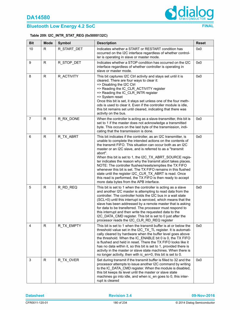
Datasheet Revision 3.4 09-Nov-2016
CFR0011-120-01 180 of 234 © 2014 Dialog Semiconductor
DA14580
Bluetooth Low Energy 4.2 SoC FINAL
10 R R_START_DET Indicates whether a START or RESTART condition has occurred on the I2C interface regardless of whether control-ler is operating in slave or master mode.
0x0
9 R R_STOP_DET Indicates whether a STOP condition has occurred on the I2C interface regardless of whether controller is operating in slave or master mode.
0x0
8 R R_ACTIVITY This bit captures I2C Ctrl activity and stays set until it is cleared. There are four ways to clear it:=> Disabling the I2C Ctrl=> Reading the IC_CLR_ACTIVITY register=> Reading the IC_CLR_INTR register=> System resetOnce this bit is set, it stays set unless one of the four meth-ods is used to clear it. Even if the controller module is idle, this bit remains set until cleared, indicating that there was activity on the bus.
0x0
7 R R_RX_DONE When the controller is acting as a slave-transmitter, this bit is set to 1 if the master does not acknowledge a transmitted byte. This occurs on the last byte of the transmission, indi-cating that the transmission is done.
0x0
6 R R_TX_ABRT This bit indicates if the controller, as an I2C transmitter, is unable to complete the intended actions on the contents of the transmit FIFO. This situation can occur both as an I2C master or an I2C slave, and is referred to as a "transmit abort".When this bit is set to 1, the I2C_TX_ABRT_SOURCE regis-ter indicates the reason why the transmit abort takes places.NOTE: The controller flushes/resets/empties the TX FIFO whenever this bit is set. The TX FIFO remains in this flushed state until the register I2C_CLR_TX_ABRT is read. Once this read is performed, the TX FIFO is then ready to accept more data bytes from the APB interface.
0x0
5 R R_RD_REQ This bit is set to 1 when the controller is acting as a slave and another I2C master is attempting to read data from the controller. The controller holds the I2C bus in a wait state (SCL=0) until this interrupt is serviced, which means that the slave has been addressed by a remote master that is asking for data to be transferred. The processor must respond to this interrupt and then write the requested data to the I2C_DATA_CMD register. This bit is set to 0 just after the processor reads the I2C_CLR_RD_REQ register
0x0
4 R R_TX_EMPTY This bit is set to 1 when the transmit buffer is at or below the threshold value set in the I2C_TX_TL register. It is automati-cally cleared by hardware when the buffer level goes above the threshold. When the IC_ENABLE bit 0 is 0, the TX FIFO is flushed and held in reset. There the TX FIFO looks like it has no data within it, so this bit is set to 1, provided there is activity in the master or slave state machines. When there is no longer activity, then with ic_en=0, this bit is set to 0.
0x0
3 R R_TX_OVER Set during transmit if the transmit buffer is filled to 32 and the processor attempts to issue another I2C command by writing to the IC_DATA_CMD register. When the module is disabled, this bit keeps its level until the master or slave state machines go into idle, and when ic_en goes to 0, this inter-rupt is cleared
0x0
Table 209: I2C_INTR_STAT_REG (0x5000132C)
Bit Mode Symbol Description Reset

Datasheet Revision 3.4 09-Nov-2016
CFR0011-120-01 181 of 234 © 2014 Dialog Semiconductor
DA14580
Bluetooth Low Energy 4.2 SoC FINAL
2 R R_RX_FULL Set when the receive buffer reaches or goes above the RX_TL threshold in the I2C_RX_TL register. It is automati-cally cleared by hardware when buffer level goes below the threshold. If the module is disabled (I2C_ENABLE[0]=0), the RX FIFO is flushed and held in reset; therefore the RX FIFO is not full. So this bit is cleared once the I2C_ENABLE bit 0 is programmed with a 0, regardless of the activity that contin-ues.
0x0
1 R R_RX_OVER Set if the receive buffer is completely filled to 32 and an addi-tional byte is received from an external I2C device. The con-troller acknowledges this, but any data bytes received after the FIFO is full are lost. If the module is disabled (I2C_ENABLE[0]=0), this bit keeps its level until the master or slave state machines go into idle, and when ic_en goes to 0, this interrupt is cleared.
0x0
0 R R_RX_UNDER Set if the processor attempts to read the receive buffer when it is empty by reading from the IC_DATA_CMD register. If the module is disabled (I2C_ENABLE[0]=0), this bit keeps its level until the master or slave state machines go into idle, and when ic_en goes to 0, this interrupt is cleared.
0x0
Table 209: I2C_INTR_STAT_REG (0x5000132C)
Bit Mode Symbol Description Reset
Table 210: I2C_INTR_MASK_REG (0x50001330)
Bit Mode Symbol Description Reset
15:12 - - Reserved 0x0
11 R/W M_GEN_CALL These bits mask their corresponding interrupt status bits in the I2C_INTR_STAT register.
0x1
10 R/W M_START_DET These bits mask their corresponding interrupt status bits in the I2C_INTR_STAT register.
0x0
9 R/W M_STOP_DET These bits mask their corresponding interrupt status bits in the I2C_INTR_STAT register.
0x0
8 R/W M_ACTIVITY These bits mask their corresponding interrupt status bits in the I2C_INTR_STAT register.
0x0
7 R/W M_RX_DONE These bits mask their corresponding interrupt status bits in the I2C_INTR_STAT register.
0x1
6 R/W M_TX_ABRT These bits mask their corresponding interrupt status bits in the I2C_INTR_STAT register.
0x1
5 R/W M_RD_REQ These bits mask their corresponding interrupt status bits in the I2C_INTR_STAT register.
0x1
4 R/W M_TX_EMPTY These bits mask their corresponding interrupt status bits in the I2C_INTR_STAT register.
0x1
3 R/W M_TX_OVER These bits mask their corresponding interrupt status bits in the I2C_INTR_STAT register.
0x1
2 R/W M_RX_FULL These bits mask their corresponding interrupt status bits in the I2C_INTR_STAT register.
0x1
1 R/W M_RX_OVER These bits mask their corresponding interrupt status bits in the I2C_INTR_STAT register.
0x1
0 R/W M_RX_UNDER These bits mask their corresponding interrupt status bits in the I2C_INTR_STAT register.
0x1

Datasheet Revision 3.4 09-Nov-2016
CFR0011-120-01 182 of 234 © 2014 Dialog Semiconductor
DA14580
Bluetooth Low Energy 4.2 SoC FINAL
Table 211: I2C_RAW_INTR_STAT_REG (0x50001334)
Bit Mode Symbol Description Reset
15:12 - - Reserved 0x0
11 R GEN_CALL Set only when a General Call address is received and it is acknowledged. It stays set until it is cleared either by dis-abling controller or when the CPU reads bit 0 of the I2C_CLR_GEN_CALL register. I2C Ctrl stores the received data in the Rx buffer.
0x0
10 R START_DET Indicates whether a START or RESTART condition has occurred on the I2C interface regardless of whether control-ler is operating in slave or master mode.
0x0
9 R STOP_DET Indicates whether a STOP condition has occurred on the I2C interface regardless of whether controller is operating in slave or master mode.
0x0
8 R ACTIVITY This bit captures I2C Ctrl activity and stays set until it is cleared. There are four ways to clear it:=> Disabling the I2C Ctrl=> Reading the IC_CLR_ACTIVITY register=> Reading the IC_CLR_INTR register=> System resetOnce this bit is set, it stays set unless one of the four meth-ods is used to clear it. Even if the controller module is idle, this bit remains set until cleared, indicating that there was activity on the bus.
0x0
7 R RX_DONE When the controller is acting as a slave-transmitter, this bit is set to 1 if the master does not acknowledge a transmitted byte. This occurs on the last byte of the transmission, indi-cating that the transmission is done.
0x0
6 R TX_ABRT This bit indicates if the controller, as an I2C transmitter, is unable to complete the intended actions on the contents of the transmit FIFO. This situation can occur both as an I2C master or an I2C slave, and is referred to as a "transmit abort".When this bit is set to 1, the I2C_TX_ABRT_SOURCE regis-ter indicates the reason why the transmit abort takes places.NOTE: The controller flushes/resets/empties the TX FIFO whenever this bit is set. The TX FIFO remains in this flushed state until the register I2C_CLR_TX_ABRT is read. Once this read is performed, the TX FIFO is then ready to accept more data bytes from the APB interface.
0x0
5 R RD_REQ This bit is set to 1 when I2C Ctrl is acting as a slave and another I2C master is attempting to read data from the con-troller. The controller holds the I2C bus in a wait state (SCL=0) until this interrupt is serviced, which means that the slave has been addressed by a remote master that is asking for data to be transferred. The processor must respond to this interrupt and then write the requested data to the I2C_DATA_CMD register. This bit is set to 0 just after the processor reads the I2C_CLR_RD_REQ register
0x0
4 R TX_EMPTY This bit is set to 1 when the transmit buffer is at or below the threshold value set in the I2C_TX_TL register. It is automati-cally cleared by hardware when the buffer level goes above the threshold. When the IC_ENABLE bit 0 is 0, the TX FIFO is flushed and held in reset. There the TX FIFO looks like it has no data within it, so this bit is set to 1, provided there is activity in the master or slave state machines. When there is no longer activity, then with ic_en=0, this bit is set to 0.
0x0

Datasheet Revision 3.4 09-Nov-2016
CFR0011-120-01 183 of 234 © 2014 Dialog Semiconductor
DA14580
Bluetooth Low Energy 4.2 SoC FINAL
3 R TX_OVER Set during transmit if the transmit buffer is filled to 32 and the processor attempts to issue another I2C command by writing to the IC_DATA_CMD register. When the module is disabled, this bit keeps its level until the master or slave state machines go into idle, and when ic_en goes to 0, this inter-rupt is cleared
0x0
2 R RX_FULL Set when the receive buffer reaches or goes above the RX_TL threshold in the I2C_RX_TL register. It is automati-cally cleared by hardware when buffer level goes below the threshold. If the module is disabled (I2C_ENABLE[0]=0), the RX FIFO is flushed and held in reset; therefore the RX FIFO is not full. So this bit is cleared once the I2C_ENABLE bit 0 is programmed with a 0, regardless of the activity that contin-ues.
0x0
1 R RX_OVER Set if the receive buffer is completely filled to 32 and an addi-tional byte is received from an external I2C device. The con-troller acknowledges this, but any data bytes received after the FIFO is full are lost. If the module is disabled (I2C_ENABLE[0]=0), this bit keeps its level until the master or slave state machines go into idle, and when ic_en goes to 0, this interrupt is cleared.
0x0
0 R RX_UNDER Set if the processor attempts to read the receive buffer when it is empty by reading from the IC_DATA_CMD register. If the module is disabled (I2C_ENABLE[0]=0), this bit keeps its level until the master or slave state machines go into idle, and when ic_en goes to 0, this interrupt is cleared.
0x0
Table 211: I2C_RAW_INTR_STAT_REG (0x50001334)
Bit Mode Symbol Description Reset
Table 212: I2C_RX_TL_REG (0x50001338)
Bit Mode Symbol Description Reset
15:5 - - Reserved 0x0
4:0 R/W RX_TL Receive FIFO Threshold Level Controls the level of entries (or above) that triggers the RX_FULL interrupt (bit 2 in I2C_RAW_INTR_STAT register). The valid range is 0-31, with the additional restriction that hardware does not allow this value to be set to a value larger than the depth of the buffer. If an attempt is made to do that, the actual value set will be the maximum depth of the buffer. A value of 0 sets the threshold for 1 entry, and a value of 31 sets the threshold for 32 entries.
0x0
Table 213: I2C_TX_TL_REG (0x5000133C)
Bit Mode Symbol Description Reset
15:5 - - Reserved 0x0
4:0 R/W RX_TL Transmit FIFO Threshold Level Controls the level of entries (or below) that trigger the TX_EMPTY interrupt (bit 4 in I2C_RAW_INTR_STAT register). The valid range is 0-31, with the additional restriction that it may not be set to value larger than the depth of the buffer. If an attempt is made to do that, the actual value set will be the maximum depth of the buffer. A value of 0 sets the threshold for 0 entries, and a value of 31 sets the threshold for 32 entries..
0x0

Datasheet Revision 3.4 09-Nov-2016
CFR0011-120-01 184 of 234 © 2014 Dialog Semiconductor
DA14580
Bluetooth Low Energy 4.2 SoC FINAL
Table 214: I2C_CLR_INTR_REG (0x50001340)
Bit Mode Symbol Description Reset
15:1 - - Reserved 0x0
0 R CLR_INTR Read this register to clear the combined interrupt, all individ-ual interrupts, and the I2C_TX_ABRT_SOURCE register. This bit does not clear hardware clearable interrupts but soft-ware clearable interrupts. Refer to Bit 9 of the I2C_TX_ABRT_SOURCE register for an exception to clear-ing I2C_TX_ABRT_SOURCE
0x0
Table 215: I2C_CLR_RX_UNDER_REG (0x50001344)
Bit Mode Symbol Description Reset
15:1 - - Reserved 0x0
0 R CLR_RX_UNDER Read this register to clear the RX_UNDER interrupt (bit 0) of theI2C_RAW_INTR_STAT register.
0x0
Table 216: I2C_CLR_RX_OVER_REG (0x50001348)
Bit Mode Symbol Description Reset
15:1 - - Reserved 0x0
0 R CLR_RX_OVER Read this register to clear the RX_OVER interrupt (bit 1) of theI2C_RAW_INTR_STAT register.
0x0
Table 217: I2C_CLR_TX_OVER_REG (0x5000134C)
Bit Mode Symbol Description Reset
15:1 - - Reserved 0x0
0 R CLR_TX_OVER Read this register to clear the TX_OVER interrupt (bit 3) of the I2C_RAW_INTR_STAT register.
0x0
Table 218: I2C_CLR_RD_REQ_REG (0x50001350)
Bit Mode Symbol Description Reset
15:1 - - Reserved 0x0
0 R CLR_RD_REQ Read this register to clear the RD_REQ interrupt (bit 5) of the I2C_RAW_INTR_STAT register.
0x0
Table 219: I2C_CLR_TX_ABRT_REG (0x50001354)
Bit Mode Symbol Description Reset
15:1 - - Reserved 0x0
0 R CLR_TX_ABRT Read this register to clear the TX_ABRT interrupt (bit 6) of theIC_RAW_INTR_STAT register, and the I2C_TX_ABRT_SOURCE register. This also releases the TX FIFO from the flushed/reset state, allowing more writes to the TX FIFO. Refer to Bit 9 of the I2C_TX_ABRT_SOURCE register for an exception to clearing IC_TX_ABRT_SOURCE.
0x0

Datasheet Revision 3.4 09-Nov-2016
CFR0011-120-01 185 of 234 © 2014 Dialog Semiconductor
DA14580
Bluetooth Low Energy 4.2 SoC FINAL
Table 220: I2C_CLR_RX_DONE_REG (0x50001358)
Bit Mode Symbol Description Reset
15:1 - - Reserved 0x0
0 R CLR_RX_DONE Read this register to clear the RX_DONE interrupt (bit 7) of theI2C_RAW_INTR_STAT register.
0x0
Table 221: I2C_CLR_ACTIVITY_REG (0x5000135C)
Bit Mode Symbol Description Reset
15:1 - - Reserved 0x0
0 R CLR_ACTIVITY Reading this register clears the ACTIVITY interrupt if the I2C is not active anymore. If the I2C module is still active on the bus, the ACTIVITY interrupt bit continues to be set. It is auto-matically cleared by hardware if the module is disabled and if there is no further activity on the bus. The value read from this register to get status of the ACTIVITY interrupt (bit 8) of the IC_RAW_INTR_STAT register
0x0
Table 222: I2C_CLR_STOP_DET_REG (0x50001360)
Bit Mode Symbol Description Reset
15:1 - - Reserved 0x0
0 R CLR_ACTIVITY Reading this register clears the ACTIVITY interrupt if the I2C is not active anymore. If the I2C module is still active on the bus, the ACTIVITY interrupt bit continues to be set. It is auto-matically cleared by hardware if the module is disabled and if there is no further activity on the bus. The value read from this register to get status of the ACTIVITY interrupt (bit 8) of the IC_RAW_INTR_STAT register.
0x0
Table 223: I2C_CLR_START_DET_REG (0x50001364)
Bit Mode Symbol Description Reset
15:1 - - Reserved 0x0
0 R CLR_START_DET Read this register to clear the START_DET interrupt (bit 10) of the IC_RAW_INTR_STAT register.
0x0
Table 224: I2C_CLR_GEN_CALL_REG (0x50001368)
Bit Mode Symbol Description Reset
15:1 - - Reserved 0x0
0 R CLR_GEN_CALL Read this register to clear the GEN_CALL interrupt (bit 11) ofI2C_RAW_INTR_STAT register.
0x0
Table 225: I2C_ENABLE_REG (0x5000136C)
Bit Mode Symbol Description Reset
15:1 - - Reserved 0x0

Datasheet Revision 3.4 09-Nov-2016
CFR0011-120-01 186 of 234 © 2014 Dialog Semiconductor
DA14580
Bluetooth Low Energy 4.2 SoC FINAL
0 R/W CTRL_ENABLE Controls whether the controller is enabled.0: Disables the controller (TX and RX FIFOs are held in an erased state)1: Enables the controllerSoftware can disable the controller while it is active. How-ever, it is important that care be taken to ensure that the con-troller is disabled properly. When the controller is disabled, the following occurs:* The TX FIFO and RX FIFO get flushed.* Status bits in the IC_INTR_STAT register are still active until the controller goes into IDLE state.If the module is transmitting, it stops as well as deletes the contents of the transmit buffer after the current transfer is complete. If the module is receiving, the controller stops the current transfer at the end of the current byte and does not acknowledge the transfer.There is a two ic_clk delay when enabling or disabling the controller
0x0
Table 225: I2C_ENABLE_REG (0x5000136C)
Bit Mode Symbol Description Reset
Table 226: I2C_STATUS_REG (0x50001370)
Bit Mode Symbol Description Reset
15:7 - - Reserved 0x0
6 R SLV_ACTIVITY Slave FSM Activity Status. When the Slave Finite State Machine (FSM) is not in the IDLE state, this bit is set.0: Slave FSM is in IDLE state so the Slave part of the con-troller is not Active1: Slave FSM is not in IDLE state so the Slave part of the controller is Active
0x0
5 R MST_ACTIVITY Master FSM Activity Status. When the Master Finite State Machine (FSM) is not in the IDLE state, this bit is set.0: Master FSM is in IDLE state so the Master part of the con-troller is not Active1: Master FSM is not in IDLE state so the Master part of the controller is Active
0x0
4 R RFF Receive FIFO Completely Full. When the receive FIFO is completely full, this bit is set. When the receive FIFO con-tains one or more empty location, this bit is cleared.0: Receive FIFO is not full1: Receive FIFO is full
0x0
3 R RFNE Receive FIFO Not Empty. This bit is set when the receive FIFO contains one or more entries; it is cleared when the receive FIFO is empty.0: Receive FIFO is empty1: Receive FIFO is not empty
0x0
2 R TFE Transmit FIFO Completely Empty. When the transmit FIFO is completely empty, this bit is set. When it contains one or more valid entries, this bit is cleared. This bit field does not request an interrupt.0: Transmit FIFO is not empty1: Transmit FIFO is empty
0x1
1 R TFNF Transmit FIFO Not Full. Set when the transmit FIFO contains one or more empty locations, and is cleared when the FIFO is full.0: Transmit FIFO is full1: Transmit FIFO is not full
0x1

Datasheet Revision 3.4 09-Nov-2016
CFR0011-120-01 187 of 234 © 2014 Dialog Semiconductor
DA14580
Bluetooth Low Energy 4.2 SoC FINAL
0 R I2C_ACTIVITY I2C Activity Status. 0x0
Table 226: I2C_STATUS_REG (0x50001370)
Bit Mode Symbol Description Reset
Table 227: I2C_TXFLR_REG (0x50001374)
Bit Mode Symbol Description Reset
15:6 - - Reserved 0x0
5:0 R TXFLR Transmit FIFO Level. Contains the number of valid data entries in the transmit FIFO. Size is constrained by the TXFLR value
0x0
Table 228: I2C_RXFLR_REG (0x50001378)
Bit Mode Symbol Description Reset
15:6 - - Reserved 0x0
5:0 R RXFLR Receive FIFO Level. Contains the number of valid data entries in the receive FIFO. Size is constrained by the RXFLR value
0x0
Table 229: I2C_SDA_HOLD_REG (0x5000137C)
Bit Mode Symbol Description Reset
15:0 R/W IC_SDA_HOLD SDA Hold time 0x1
Table 230: I2C_TX_ABRT_SOURCE_REG (0x50001380)
Bit Mode Symbol Description Reset
15 R ABRT_SLVRD_INTX 1: When the processor side responds to a slave mode request for data to be transmitted to a remote master and user writes a 1 in CMD (bit 8) of 2IC_DATA_CMD register
0x0
14 R ABRT_SLV_ARBLOST
1: Slave lost the bus while transmitting data to a remote master.I2C_TX_ABRT_SOURCE[12] is set at the same time. Note: Even though the slave never "owns" the bus, something could go wrong on the bus. This is a fail safe check. For instance, during a data transmission at the low-to-high tran-sition of SCL, if what is on the data bus is not what is sup-posed to be transmitted, then the controller no longer own the bus.
0x0
13 R ABRT_SLVFLUSH_TXFIFO
1: Slave has received a read command and some data exists in the TX FIFO so the slave issues a TX_ABRT inter-rupt to flush old data in TX FIFO.
0x0
12 R ARB_LOST 1: Master has lost arbitration, or if I2C_TX_ABRT_SOURCE[14] is also set, then the slave transmitter has lost arbitration. Note: I2C can be both master and slave at the same time.
0x0
11 R ABRT_MASTER_DIS 1: User tries to initiate a Master operation with the Master mode disabled.
0x0
10 R ABRT_10B_RD_NORSTRT
1: The restart is disabled (IC_RESTART_EN bit (I2C_CON[5]) = 0) and the master sends a read command in 10-bit addressing mode.
0x0

Datasheet Revision 3.4 09-Nov-2016
CFR0011-120-01 188 of 234 © 2014 Dialog Semiconductor
DA14580
Bluetooth Low Energy 4.2 SoC FINAL
9 R ABRT_SBYTE_NORSTRT
To clear Bit 9, the source of the ABRT_SBYTE_NORSTRT must be fixed first; restart must be enabled (I2C_CON[5]=1), the SPECIAL bit must be cleared (I2C_TAR[11]), or the GC_OR_START bit must be cleared (I2C_TAR[10]). Once the source of the ABRT_SBYTE_NORSTRT is fixed, then this bit can be cleared in the same manner as other bits in this register. If the source of the ABRT_SBYTE_NORSTRT is not fixed before attempting to clear this bit, bit 9 clears for one cycle and then gets re-asserted. 1: The restart is dis-abled (IC_RESTART_EN bit (I2C_CON[5]) = 0) and the user is trying to send a START Byte.
0x0
8 R ABRT_HS_NORSTRT
1: The restart is disabled (IC_RESTART_EN bit (I2C_CON[5]) = 0) and the user is trying to use the master to transfer data in High Speed mode
0x0
7 R ABRT_SBYTE_ACKDET
1: Master has sent a START Byte and the START Byte was acknowledged (wrong behavior).
0x0
6 R ABRT_HS_ACKDET 1: Master is in High Speed mode and the High Speed Master code was acknowledged (wrong behavior).
0x0
5 R ABRT_GCALL_READ
1: the controller in master mode sent a General Call but the user programmed the byte following the General Call to be a read from the bus (IC_DATA_CMD[9] is set to 1).
0x0
4 R ABRT_GCALL_NOACK
1: the controller in master mode sent a General Call and no slave on the bus acknowledged the General Call.
0x0
3 R ABRT_TXDATA_NOACK
1: This is a master-mode only bit. Master has received an acknowledgement for the address, but when it sent data byte(s) following the address, it did not receive an acknowl-edge from the remote slave(s).
0x0
2 R ABRT_10ADDR2_NOACK
1: Master is in 10-bit address mode and the second address byte of the 10-bit address was not acknowledged by any slave.
0x0
1 R ABRT_10ADDR1_NOACK
1: Master is in 10-bit address mode and the first 10-bit address byte was not acknowledged by any slave.
0x0
0 R ABRT_7B_ADDR_NOACK
1: Master is in 7-bit addressing mode and the address sent was not acknowledged by any slave.
0x0
Table 230: I2C_TX_ABRT_SOURCE_REG (0x50001380)
Bit Mode Symbol Description Reset
Table 231: I2C_SDA_SETUP_REG (0x50001394)
Bit Mode Symbol Description Reset
15:8 - - Reserved 0x0
7:0 R/W SDA_SETUP SDA Setup.This register controls the amount of time delay (number of I2C clock periods) between the rising edge of SCL and SDA changing by holding SCL low when I2C block services a read request while operating as a slave-transmitter. The rele-vant I2C requirement is tSU:DAT (note 4) as detailed in the I2C Bus Specification. This register must be programmed with a value equal to or greater than 2.It is recommended that if the required delay is 1000ns, then for an I2C frequency of 10 MHz, IC_SDA_SETUP should be programmed to a value of 11.Writes to this register succeed only when IC_ENABLE[0] = 0.
0x64

Datasheet Revision 3.4 09-Nov-2016
CFR0011-120-01 189 of 234 © 2014 Dialog Semiconductor
DA14580
Bluetooth Low Energy 4.2 SoC FINAL
Table 232: I2C_ACK_GENERAL_CALL_REG (0x50001398)
Bit Mode Symbol Description Reset
15:1 - - Reserved 0x0
0 R/W ACK_GEN_CALL ACK General Call. When set to 1, I2C Ctrl responds with a ACK (by asserting ic_data_oe) when it receives a General Call. When set to 0, the controller does not generate General Call interrupts.
0x0
Table 233: I2C_ENABLE_STATUS_REG (0x5000139C)
Bit Mode Symbol Description Reset
15:3 - - Reserved 0x0
2 R SLV_RX_DATA_LOST
Slave Received Data Lost. This bit indicates if a Slave-Receiveroperation has been aborted with at least one data byte received from an I2C transfer due to the setting of IC_ENABLE from 1 to 0. When read as 1, the controller is deemed to have been actively engaged in an aborted I2C transfer (with matching address) and the data phase of the I2C transfer has been entered, even though a data byte has been responded with a NACK. NOTE: If the remote I2C mas-ter terminates the transfer with a STOP condition before the controller has a chance to NACK a transfer, and IC_ENABLE has been set to 0, then this bit is also set to 1.When read as 0, the controller is deemed to have been dis-abled without being actively involved in the data phase of a Slave-Receiver transfer.NOTE: The CPU can safely read this bit when IC_EN (bit 0) is read as 0.
0x0
1 R SLV_DISABLED_WHILE_BUSY
Slave Disabled While Busy (Transmit, Receive). This bit indi-cates if a potential or active Slave operation has been aborted due to the setting of the IC_ENABLE register from 1 to 0. This bit is set when the CPU writes a 0 to the IC_ENABLE register while:(a) I2C Ctrl is receiving the address byte of the Slave-Trans-mitter operation from a remote master; OR,(b) address and data bytes of the Slave-Receiver operation from a remote master. When read as 1, the controller is deemed to have forced a NACK during any part of an I2C transfer, irrespective of whether the I2C address matches the slave address set in I2C Ctrl (IC_SAR register) OR if the transfer is completed before IC_ENABLE is set to 0 but has not taken effect.NOTE: If the remote I2C master terminates the transfer with a STOP condition before the the controller has a chance to NACK a transfer, and IC_ENABLE has been set to 0, then this bit will also be set to 1.When read as 0, the controller is deemed to have been dis-abled when there is master activity, or when the I2C bus is idle.NOTE: The CPU can safely read this bit when IC_EN (bit 0) is read as 0.
0x0

Datasheet Revision 3.4 09-Nov-2016
CFR0011-120-01 190 of 234 © 2014 Dialog Semiconductor
DA14580
Bluetooth Low Energy 4.2 SoC FINAL
0 R IC_EN ic_en Status. This bit always reflects the value driven on the output port ic_en. When read as 1, the controller is deemed to be in an enabled state.When read as 0, the controller is deemed completely inac-tive.NOTE: The CPU can safely read this bit anytime. When this bit is read as 0, the CPU can safely read SLV_RX_DATA_LOST (bit 2) and SLV_DISABLED_WHILE_BUSY (bit 1).
0x0
Table 233: I2C_ENABLE_STATUS_REG (0x5000139C)
Bit Mode Symbol Description Reset
Table 234: I2C_IC_FS_SPKLEN_REG (0x500013A0)
Bit Mode Symbol Description Reset
15:8 - - Reserved 0x0
7:0 R/W IC_FS_SPKLEN This register must be set before any I2C bus transaction can take place to ensure stable operation. This register sets the duration, measured in ic_clk cycles, of the longest spike in the SCL or SDA lines that will be filtered out by the spike suppression logic. This register can be written only when the I2C interface is disabled which corresponds to the IC_ENABLE register being set to 0. Writes at other times have no effect. The minimum valid value is 2; hardware pre-vents values less than this being written, and if attempted results in 2 being set.
0x1
Table 235: GPIO_IRQ0_IN_SEL_REG (0x50001400)
Bit Mode Symbol Description Reset
15:6 - - Reserved 0x0

Datasheet Revision 3.4 09-Nov-2016
CFR0011-120-01 191 of 234 © 2014 Dialog Semiconductor
DA14580
Bluetooth Low Energy 4.2 SoC FINAL
5:0 R/W KBRD_IRQ0_SEL input selection that can generate a GPIO interrupt0: no input selected1: P0[0] is selected2: P0[1] is selected3: P0[2] is selected4: P0[3] is selected5: P0[4] is selected6: P0[5] is selected7: P0[6] is selected8: P0[7] is selected9: P1[0] is selected10: P1[1] is selected11: P1[2] is selected12: P1[3] is selected13: P1[4] is selected14: P1[5] is selected15: P2[0] is selected16: P2[1] is selected17: P2[2] is selected18: P2[3] is selected19: P2[4] is selected20: P2[5] is selected21: P2[6] is selected22: P2[7] is selected23: P2[8] is selected24: P2[9] is selected25: P3[0] is selected26: P3[1] is selected27: P3[2] is selected28: P3[3] is selected29: P3[4] is selected30: P3[5] is selected31: P3[6] is selected32: P3[7] is selectedall others: no input selected
0x0
Table 235: GPIO_IRQ0_IN_SEL_REG (0x50001400)
Bit Mode Symbol Description Reset
Table 236: GPIO_IRQ1_IN_SEL_REG (0x50001402)
Bit Mode Symbol Description Reset
15:5 - - Reserved 0x0
5:0 R/W KBRD_IRQ1_SEL see KBRD_IRQ0_SEL 0x0
Table 237: GPIO_IRQ2_IN_SEL_REG (0x50001404)
Bit Mode Symbol Description Reset
15:5 - - Reserved 0x0
5:0 R/W KBRD_IRQ2_SEL see KBRD_IRQ0_SEL 0x0
Table 238: GPIO_IRQ3_IN_SEL_REG (0x50001406)
Bit Mode Symbol Description Reset
15:5 - - Reserved 0x0
5:0 R/W KBRD_IRQ3_SEL see KBRD_IRQ0_SEL 0x0

Datasheet Revision 3.4 09-Nov-2016
CFR0011-120-01 192 of 234 © 2014 Dialog Semiconductor
DA14580
Bluetooth Low Energy 4.2 SoC FINAL
Table 239: GPIO_IRQ4_IN_SEL_REG (0x50001408)
Bit Mode Symbol Description Reset
15:5 - - Reserved 0x0
5:0 R/W KBRD_IRQ4_SEL see KBRD_IRQ0_SEL 0x0
Table 240: GPIO_DEBOUNCE_REG (0x5000140C)
Bit Mode Symbol Description Reset
15:14 - - Reserved 0x0
13 R/W DEB_ENABLE_KBRD
enables the debounce counter for the KBRD interface 0x0
12 R/W DEB_ENABLE4 enables the debounce counter for GPIO IRQ4 0x0
11 R/W DEB_ENABLE3 enables the debounce counter for GPIO IRQ3 0x0
10 R/W DEB_ENABLE2 enables the debounce counter for GPIO IRQ2 0x0
9 R/W DEB_ENABLE1 enables the debounce counter for GPIO IRQ1 0x0
8 R/W DEB_ENABLE0 enables the debounce counter for GPIO IRQ0 0x0
7:6 - - Reserved 0x0
5:0 R/W DEB_VALUE Keyboard debounce time if enabled. Generate KEYB_INT after specified time.Debounce time: N*1 ms. N =0..63
0x0
Table 241: GPIO_RESET_IRQ_REG (0x5000140E)
Bit Mode Symbol Description Reset
15:6 - - Reserved 0x0
5 R0/W RESET_KBRD_IRQ writing a 1 to this bit will reset the KBRD IRQ.Reading returns 0.
0x0
4 R0/W RESET_GPIO4_IRQ writing a 1 to this bit will reset the GPIO4 IRQ.Reading returns 0.
0x0
3 R0/W RESET_GPIO3_IRQ writing a 1 to this bit will reset the GPIO3 IRQ.Reading returns 0.
0x0
2 R0/W RESET_GPIO2_IRQ writing a 1 to this bit will reset the GPIO2 IRQ.Reading returns 0.
0x0
1 R0/W RESET_GPIO1_IRQ writing a 1 to this bit will reset the GPIO1 IRQ.Reading returns 0.
0x0
0 R0/W RESET_GPIO0_IRQ writing a 1 to this bit will reset the GPIO0 IRQ.Reading returns 0.
0x0
Table 242: GPIO_INT_LEVEL_CTRL_REG (0x50001410)
Bit Mode Symbol Description Reset
15:14 - - Reserved 0x0
12 R/W EDGE_LEVELN4 see EDGE_LEVELn0, but for GPIO IRQ4 0x0
11 R/W EDGE_LEVELN3 see EDGE_LEVELn0, but for GPIO IRQ3 0x0
10 R/W EDGE_LEVELN2 see EDGE_LEVELn0, but for GPIO IRQ2 0x0
9 R/W EDGE_LEVELN1 see EDGE_LEVELn0, but for GPIO IRQ1 0x0
8 R/W EDGE_LEVELN0 0: do not wait for key release after interrupt was reset for GPIO IRQ0, so a new interrupt can be initiated immediately1: wait for key release after interrupt was reset for IRQ0
0x0
7:6 - - Reserved 0x0

Datasheet Revision 3.4 09-Nov-2016
CFR0011-120-01 193 of 234 © 2014 Dialog Semiconductor
DA14580
Bluetooth Low Energy 4.2 SoC FINAL
4 R/W INPUT_LEVEL4 see INPUT_LEVEL0, but for GPIO IRQ4 0x0
3 R/W INPUT_LEVEL3 see INPUT_LEVEL0, but for GPIO IRQ3 0x0
2 R/W INPUT_LEVEL2 see INPUT_LEVEL0, but for GPIO IRQ2 0x0
1 R/W INPUT_LEVEL1 see INPUT_LEVEL0, but for GPIO IRQ1 0x0
0 R/W INPUT_LEVEL0 0 = selected input will generate GPIO IRQ0 if that input is high.1 = selected input will generate GPIO IRQ0 if that input is low.
0x0
Table 242: GPIO_INT_LEVEL_CTRL_REG (0x50001410)
Bit Mode Symbol Description Reset
Table 243: KBRD_IRQ_IN_SEL0_REG (0x50001412)
Bit Mode Symbol Description Reset
15 R/W KBRD_REL 0 = No interrupt on key release1 = Interrupt also on key release (also debouncing if enabled)
0x0
14 R/W KBRD_LEVEL 0 = enabled input will generate KBRD IRQ if that input is high.1 = enabled input will generate KBRD IRQ if that input is low.
0x0
13:8 R/W KEY_REPEAT While key is pressed, automatically generate repeatingKEYB_INT after specified time unequal to 0.Repeat time: N*1 ms. N =1..63, N=0 disables the timer.
0x0
7 R/W KBRD_P07_EN enable P0[7] for the keyboard interrupt 0x0
6 R/W KBRD_P06_EN enable P0[6] for the keyboard interrupt 0x0
5 R/W KBRD_P05_EN enable P0[5] for the keyboard interrupt 0x0
4 R/W KBRD_P04_EN enable P0[4] for the keyboard interrupt 0x0
3 R/W KBRD_P03_EN enable P0[3] for the keyboard interrupt 0x0
2 R/W KBRD_P02_EN enable P0[2] for the keyboard interrupt 0x0
1 R/W KBRD_P01_EN enable P0[1] for the keyboard interrupt 0x0
0 R/W KBRD_P00_EN enable P0[0] for the keyboard interrupt 0x0
Table 244: KBRD_IRQ_IN_SEL1_REG (0x50001414)
Bit Mode Symbol Description Reset
15 R/W KBRD_P15_EN enable P1[5] for the keyboard interrupt 0x0
14 R/W KBRD_P14_EN enable P1[4] for the keyboard interrupt 0x0
13 R/W KBRD_P13_EN enable P1[3] for the keyboard interrupt 0x0
12 R/W KBRD_P12_EN enable P1[2] for the keyboard interrupt 0x0
11 R/W KBRD_P11_EN enable P1[1] for the keyboard interrupt 0x0
10 R/W KBRD_P10_EN enable P1[0] for the keyboard interrupt 0x0
9 R/W KBRD_P29_EN enable P2[9] for the keyboard interrupt 0x0
8 R/W KBRD_P28_EN enable P2[8] for the keyboard interrupt 0x0
7 R/W KBRD_P27_EN enable P2[7] for the keyboard interrupt 0x0
6 R/W KBRD_P26_EN enable P2[6] for the keyboard interrupt 0x0
5 R/W KBRD_P25_EN enable P2[5] for the keyboard interrupt 0x0
4 R/W KBRD_P24_EN enable P2[4] for the keyboard interrupt 0x0
3 R/W KBRD_P23_EN enable P2[3] for the keyboard interrupt 0x0
2 R/W KBRD_P22_EN enable P2[2] for the keyboard interrupt 0x0

Datasheet Revision 3.4 09-Nov-2016
CFR0011-120-01 194 of 234 © 2014 Dialog Semiconductor
DA14580
Bluetooth Low Energy 4.2 SoC FINAL
1 R/W KBRD_P21_EN enable P2[1] for the keyboard interrupt 0x0
0 R/W KBRD_P20_EN enable P2[0] for the keyboard interrupt 0x0
Table 244: KBRD_IRQ_IN_SEL1_REG (0x50001414)
Bit Mode Symbol Description Reset
Table 245: KBRD_IRQ_IN_SEL2_REG (0x50001416)
Bit Mode Symbol Description Reset
7 R/W KBRD_P37_EN enable P3[7] for the keyboard interrupt 0x0
6 R/W KBRD_P36_EN enable P3[6] for the keyboard interrupt 0x0
5 R/W KBRD_P35_EN enable P3[5] for the keyboard interrupt 0x0
4 R/W KBRD_P34_EN enable P3[4] for the keyboard interrupt 0x0
3 R/W KBRD_P33_EN enable P3[3] for the keyboard interrupt 0x0
2 R/W KBRD_P32_EN enable P3[2] for the keyboard interrupt 0x0
1 R/W KBRD_P31_EN enable P3[1] for the keyboard interrupt 0x0
0 R/W KBRD_P30_EN enable P3[0] for the keyboard interrupt 0x0
Table 246: GP_ADC_CTRL_REG (0x50001500)
Bit Mode Symbol Description Reset
15 R/W GP_ADC_LDO_ZERO
Forces LDO-output to 0V. 0x0
14 R/W GP_ADC_LDO_EN Turns on LDO. 0x0
13 R/W GP_ADC_CHOP Takes two samples with opposite GP_ADC_SIGN to cancel the internal offset voltage of the ADC; Highly recommended for DC-measurements.
0x0
12 R/W GP_ADC_MUTE Takes sample at mid-scale (to dertermine the internal offset and/or noise of the ADC with regards to VDD_REF which is also sampled by the ADC).
0x0
11 R/W GP_ADC_SE 0 = Differential mode1 = Single ended mode
0x0
10 R/W GP_ADC_SIGN 0 = Default1 = Conversion with opposite sign at input and output to can-cel out the internal offset of the ADC and low-frequency
0x0
9:6 R/W GP_ADC_SEL ADC input selection which must be set before the GP_ADC_START bit is enabled.If GP_ADC_SE = 1 (single ended mode):0000 = P0[0]0001 = P0[1]0010 = P0[2]0011 = P0[3]0100 = AVS0101 = VDD_REF0110 = VDD_RTT0111 = VBAT3V1000 = VDCDC1001 = VBAT1VAll other combinations are reserved.If GP_ADC_SE = 0 (differential mode):0000 = P0[0] vs P0[1]All other combinations are P0[2] vs P0[3].
0x0
5 R/W GP_ADC_MINT 0 = Disable (mask) GP_ADC_INT.1 = Enable GP_ADC_INT to ICU.
0x0

Datasheet Revision 3.4 09-Nov-2016
CFR0011-120-01 195 of 234 © 2014 Dialog Semiconductor
DA14580
Bluetooth Low Energy 4.2 SoC FINAL
4 R GP_ADC_INT 1 = AD conversion ready and has generated an interrupt. Must be cleared by writing any value to GP_ADC_CLEAR_INT_REG.
0x0
3 R/W GP_ADC_CLK_SEL 0 = Internal high-speed ADC clock used.1 = Digital clock used.
0x0
2 - GP_ADC_TEST Reserved, keep 0. 0x0
1 R/W GP_ADC_START 0 = ADC conversion ready.1 = If a 1 is written, the ADC starts a conversion. After the conversion this bit will be set to 0 and the GP_ADC_INT bit will be set.
0x0
0 R/W GP_ADC_EN 0 = ADC is disabled and in reset.1 = ADC is enabled and sampling of input is started.
0x0
Table 246: GP_ADC_CTRL_REG (0x50001500)
Bit Mode Symbol Description Reset
Table 247: GP_ADC_CTRL2_REG (0x50001502)
Bit Mode Symbol Description Reset
15:4 - - Reserved 0x0
3 R/W GP_ADC_I20U Adds 20uA constant load current at the ADC LDO to mini-mize ripple on the reference voltage of the ADC.
0x0
2 R/W GP_ADC_IDYN Enables dynamic load current at the ADC LDO to minimize ripple on the reference voltage of the ADC.
0x0
1 R/W GP_ADC_ATTN3X 0 = Input voltages up to 1.2V allowed.1 = Input voltages up to 3.6V allowed by enabling 3x attenu-ator.
0x0
0 R/W GP_ADC_DELAY_EN
Enables delay function for several signals. This is not auto-cleared. Toggle this bit before every sampling to enable suc-cesive conversions.
0x0
Table 248: GP_ADC_OFFP_REG (0x50001504)
Bit Mode Symbol Description Reset
15:10 - - Reserved 0x0
9:0 R/W GP_ADC_OFFP Offset adjust of 'positive' array of ADC-network (effective if "GP_ADC_SE=0", or "GP_ADC_SE=1 AND GP_ADC_SIGN=0")
0x200
Table 249: GP_ADC_OFFN_REG (0x50001506)
Bit Mode Symbol Description Reset
15:10 - - Reserved 0x0
9:0 R/W GP_ADC_OFFN Offset adjust of 'negative' array of ADC-network (effective if "GP_ADC_SE=0", or "GP_ADC_SE=1 AND GP_ADC_SIGN=1")
0x200
Table 250: GP_ADC_CLEAR_INT_REG (0x50001508)
Bit Mode Symbol Description Reset
15:0 R0/W GP_ADC_CLR_INT Writing any value to this register will clear the ADC_INT interrupt. Reading returns 0.
0x0

Datasheet Revision 3.4 09-Nov-2016
CFR0011-120-01 196 of 234 © 2014 Dialog Semiconductor
DA14580
Bluetooth Low Energy 4.2 SoC FINAL
Table 251: GP_ADC_RESULT_REG (0x5000150A)
Bit Mode Symbol Description Reset
15:10 - - Reserved 0x0
9:0 R GP_ADC_VAL Returns the 10 bits linear value of the last AD conversion. 0x0
Table 252: GP_ADC_DELAY_REG (0x5000150C)
Bit Mode Symbol Description Reset
15:8 - - Reserved 0x0
7:0 R/W DEL_LDO_EN Defines the delay before the LDO enable (GP_ADC_LDO_EN). Reset value is 0 µs since the LDO enable should be the first thing to be programmed in the sequence of bringing the GP ADC up.
0x0
Table 253: GP_ADC_DELAY2_REG (0x5000150E)
Bit Mode Symbol Description Reset
15:8 R/W DEL_ADC_START Defines the delay for the GP_ADC_START bit. Reset value is 17 µs which is the recommended value to wait before starting the GP ADC. This is the third and last step of bring-ing up the GP ADC
0x88
7:0 R/W DEL_ADC_EN Defines the delay for the GP_ADC_EN bit. Reset value is 16 µs which is the recommended value to wait after enabling the LDO. This is the second step in bringing up the GP ADC.
0x80
Table 254: CLK_REF_SEL_REG (0x50001600)
Bit Mode Symbol Description Reset
15:3 - - Reserved 0x0
2 R/W REF_CAL_START Writing a '1' starts a calibration. This bit is cleared when cali-bration is finished, and CLK_REF_VAL is ready.
0x0
1:0 R/W REF_CLK_SEL Select clock input for calibration:0x0 : RC32KHz oscillator
0x1 : RC16MHz oscillator
0x2 : XTAL32KHz oscillator
0x3 : RCX32KHz oscillator
0x0
Table 255: CLK_REF_CNT_REG (0x50001602)
Bit Mode Symbol Description Reset
15:0 R/W REF_CNT_VAL Indicates the calibration time, with a decrement counter to 1. 0x0
Table 256: CLK_REF_VAL_L_REG (0x50001604)
Bit Mode Symbol Description Reset
15:0 R XTAL_CNT_VAL Returns the lower 16 bits of XTAL16 clock cycles during the calibration time, defined with REF_CNT_VAL
0x0

Datasheet Revision 3.4 09-Nov-2016
CFR0011-120-01 197 of 234 © 2014 Dialog Semiconductor
DA14580
Bluetooth Low Energy 4.2 SoC FINAL
Table 257: CLK_REF_VAL_H_REG (0x50001606)
Bit Mode Symbol Description Reset
15:0 R XTAL_CNT_VAL Returns the upper 16 bits of XTAL16 clock cycles during the calibration time, defined with REF_CNT_VAL
0x0
Table 258: P0_DATA_REG (0x50003000)
Bit Mode Symbol Description Reset
15:8 - - Reserved 0x0
7:0 R/W P0_DATA Set P0 output register when written; Returns the value of P0 port when read
0x0
Table 259: P0_SET_DATA_REG (0x50003002)
Bit Mode Symbol Description Reset
15:8 - - Reserved 0x0
7:0 R/W P0_SET Writing a 1 to P0[y] sets P0[y] to 1. Writing 0 is discarded;Reading returns 0
0x0
Table 260: P0_RESET_DATA_REG (0x50003004)
Bit Mode Symbol Description Reset
15:8 - - Reserved 0x0
7:0 R/W P0_RESET Writing a 1 to P0[y] sets P0[y] to 0. Writing 0 is discarded;Reading returns 0
0x0
Table 261: P00_MODE_REG (0x50003006)
Bit Mode Symbol Description Reset
15:10 - - Reserved 0x0
9:8 R/W PUPD 00 = Input, no resistors selected01 = Input, pull-up selected10 = Input, Pull-down selected11 = Output, no resistors selectedIn ADC mode, these bits are don't care
0x2
7:5 - - Reserved 0x0

Datasheet Revision 3.4 09-Nov-2016
CFR0011-120-01 198 of 234 © 2014 Dialog Semiconductor
DA14580
Bluetooth Low Energy 4.2 SoC FINAL
4:0 R/W PID Function of port0 = Port function, PUPD as set above1 = UART1_RX2 = UART1_TX3 = UART2_RX4 = UART2_TX5 = SPI_DI6 = SPI_DO7 = SPI_CLK8 = SPI_EN9 = I2C_SCL10 = I2C_SDA11 = UART1_IRDA_RX12 = UART1_IRDA_TX13 = UART2_IRDA_RX14 = UART2_IRDA_TX15 = ADC (only for P0[3:0])16 = PWM017 = PWM118 = BLE_DIAG (only for P0[7:0])19 = UART1_CTSN20 = UART1_RTSN21 = UART2_CTSN22 = UART2_RTSN23 = PWM224 = PWM325 = PWM4Note: when a certain input function (like SPI_DI) is selected on more than 1 port pin, the port with the lowest index has the highest priority and P0 has higher priority than P1.
0x0
Table 261: P00_MODE_REG (0x50003006)
Bit Mode Symbol Description Reset
Table 262: P01_MODE_REG (0x50003008)
Bit Mode Symbol Description Reset
15:10 - - Reserved 0x0
9:8 R/W PUPD 00 = Input, no resistors selected01 = Input, pull-up selected10 = Input, Pull-down selected11 = Output, no resistors selectedIn ADC mode, these bits are don't care
0x2
7:5 - - Reserved 0x0

Datasheet Revision 3.4 09-Nov-2016
CFR0011-120-01 199 of 234 © 2014 Dialog Semiconductor
DA14580
Bluetooth Low Energy 4.2 SoC FINAL
4:0 R/W PID Function of port0 = Port function, PUPD as set above1 = UART1_RX2 = UART1_TX3 = UART2_RX4 = UART2_TX5 = SPI_DI6 = SPI_DO7 = SPI_CLK8 = SPI_EN9 = I2C_SCL10 = I2C_SDA11 = UART1_IRDA_RX12 = UART1_IRDA_TX13 = UART2_IRDA_RX14 = UART2_IRDA_TX15 = ADC (only for P0[3:0])16 = PWM017 = PWM118 = BLE_DIAG (only for P0[7:0])19 = UART1_CTSN20 = UART1_RTSN21 = UART2_CTSN22 = UART2_RTSN23 = PWM224 = PWM325 = PWM4Note: when a certain input function (like SPI_DI) is selected on more than 1 port pin, the port with the lowest index has the highest priority and P0 has higher priority than P1.
0x0
Table 262: P01_MODE_REG (0x50003008)
Bit Mode Symbol Description Reset
Table 263: P02_MODE_REG (0x5000300A)
Bit Mode Symbol Description Reset
15:10 - - Reserved 0x0
9:8 R/W PUPD 00 = Input, no resistors selected01 = Input, pull-up selected10 = Input, Pull-down selected11 = Output, no resistors selectedIn ADC mode, these bits are don't care
0x2
7:5 - - Reserved 0x0

Datasheet Revision 3.4 09-Nov-2016
CFR0011-120-01 200 of 234 © 2014 Dialog Semiconductor
DA14580
Bluetooth Low Energy 4.2 SoC FINAL
4:0 R/W PID Function of port0 = Port function, PUPD as set above1 = UART1_RX2 = UART1_TX3 = UART2_RX4 = UART2_TX5 = SPI_DI6 = SPI_DO7 = SPI_CLK8 = SPI_EN9 = I2C_SCL10 = I2C_SDA11 = UART1_IRDA_RX12 = UART1_IRDA_TX13 = UART2_IRDA_RX14 = UART2_IRDA_TX15 = ADC (only for P0[3:0])16 = PWM017 = PWM118 = BLE_DIAG (only for P0[7:0])19 = UART1_CTSN20 = UART1_RTSN21 = UART2_CTSN22 = UART2_RTSN23 = PWM224 = PWM325 = PWM4Note: when a certain input function (like SPI_DI) is selected on more than 1 port pin, the port with the lowest index has the highest priority and P0 has higher priority than P1.
0x0
Table 263: P02_MODE_REG (0x5000300A)
Bit Mode Symbol Description Reset
Table 264: P03_MODE_REG (0x5000300C)
Bit Mode Symbol Description Reset
15:10 - - Reserved 0x0
9:8 R/W PUPD 00 = Input, no resistors selected01 = Input, pull-up selected10 = Input, Pull-down selected11 = Output, no resistors selectedIn ADC mode, these bits are don't care
0x2
7:5 - - Reserved 0x0

Datasheet Revision 3.4 09-Nov-2016
CFR0011-120-01 201 of 234 © 2014 Dialog Semiconductor
DA14580
Bluetooth Low Energy 4.2 SoC FINAL
4:0 R/W PID Function of port0 = Port function, PUPD as set above1 = UART1_RX2 = UART1_TX3 = UART2_RX4 = UART2_TX5 = SPI_DI6 = SPI_DO7 = SPI_CLK8 = SPI_EN9 = I2C_SCL10 = I2C_SDA11 = UART1_IRDA_RX12 = UART1_IRDA_TX13 = UART2_IRDA_RX14 = UART2_IRDA_TX15 = ADC (only for P0[3:0])16 = PWM017 = PWM118 = BLE_DIAG (only for P0[7:0])19 = UART1_CTSN20 = UART1_RTSN21 = UART2_CTSN22 = UART2_RTSN23 = PWM224 = PWM325 = PWM4Note: when a certain input function (like SPI_DI) is selected on more than 1 port pin, the port with the lowest index has the highest priority and P0 has higher priority than P1.
0x0
Table 264: P03_MODE_REG (0x5000300C)
Bit Mode Symbol Description Reset
Table 265: P04_MODE_REG (0x5000300E)
Bit Mode Symbol Description Reset
15:10 - - Reserved 0x0
9:8 R/W PUPD 00 = Input, no resistors selected01 = Input, pull-up selected10 = Input, Pull-down selected11 = Output, no resistors selectedIn ADC mode, these bits are don't care
0x2
7:5 - - Reserved 0x0

Datasheet Revision 3.4 09-Nov-2016
CFR0011-120-01 202 of 234 © 2014 Dialog Semiconductor
DA14580
Bluetooth Low Energy 4.2 SoC FINAL
4:0 R/W PID Function of port0 = Port function, PUPD as set above1 = UART1_RX2 = UART1_TX3 = UART2_RX4 = UART2_TX5 = SPI_DI6 = SPI_DO7 = SPI_CLK8 = SPI_EN9 = I2C_SCL10 = I2C_SDA11 = UART1_IRDA_RX12 = UART1_IRDA_TX13 = UART2_IRDA_RX14 = UART2_IRDA_TX15 = ADC (only for P0[3:0])16 = PWM017 = PWM118 = BLE_DIAG (only for P0[7:0])19 = UART1_CTSN20 = UART1_RTSN21 = UART2_CTSN22 = UART2_RTSN23 = PWM224 = PWM325 = PWM4Note: when a certain input function (like SPI_DI) is selected on more than 1 port pin, the port with the lowest index has the highest priority and P0 has higher priority than P1.
0x0
Table 265: P04_MODE_REG (0x5000300E)
Bit Mode Symbol Description Reset
Table 266: P05_MODE_REG (0x50003010)
Bit Mode Symbol Description Reset
15:10 - - Reserved 0x0
9:8 R/W PUPD 00 = Input, no resistors selected01 = Input, pull-up selected10 = Input, Pull-down selected11 = Output, no resistors selectedIn ADC mode, these bits are don't care
0x2
7:5 - - Reserved 0x0

Datasheet Revision 3.4 09-Nov-2016
CFR0011-120-01 203 of 234 © 2014 Dialog Semiconductor
DA14580
Bluetooth Low Energy 4.2 SoC FINAL
4:0 R/W PID Function of port0 = Port function, PUPD as set above1 = UART1_RX2 = UART1_TX3 = UART2_RX4 = UART2_TX5 = SPI_DI6 = SPI_DO7 = SPI_CLK8 = SPI_EN9 = I2C_SCL10 = I2C_SDA11 = UART1_IRDA_RX12 = UART1_IRDA_TX13 = UART2_IRDA_RX14 = UART2_IRDA_TX15 = ADC (only for P0[3:0])16 = PWM017 = PWM118 = BLE_DIAG (only for P0[7:0])19 = UART1_CTSN20 = UART1_RTSN21 = UART2_CTSN22 = UART2_RTSN23 = PWM224 = PWM325 = PWM4Note: when a certain input function (like SPI_DI) is selected on more than 1 port pin, the port with the lowest index has the highest priority and P0 has higher priority than P1.
0x0
Table 266: P05_MODE_REG (0x50003010)
Bit Mode Symbol Description Reset
Table 267: P06_MODE_REG (0x50003012)
Bit Mode Symbol Description Reset
15:10 - - Reserved 0x0
9:8 R/W PUPD 00 = Input, no resistors selected01 = Input, pull-up selected10 = Input, Pull-down selected11 = Output, no resistors selectedIn ADC mode, these bits are don't care
0x2
7:5 - - Reserved 0x0
Datasheet Revision 3.4 09-Nov-2016
CFR0011-120-01 204 of 234 © 2014 Dialog Semiconductor
DA14580
Bluetooth Low Energy 4.2 SoC FINAL
4:0 R/W PID Function of port0 = Port function, PUPD as set above1 = UART1_RX2 = UART1_TX3 = UART2_RX4 = UART2_TX5 = SPI_DI6 = SPI_DO7 = SPI_CLK8 = SPI_EN9 = I2C_SCL10 = I2C_SDA11 = UART1_IRDA_RX12 = UART1_IRDA_TX13 = UART2_IRDA_RX14 = UART2_IRDA_TX15 = ADC (only for P0[3:0])16 = PWM017 = PWM118 = BLE_DIAG (only for P0[7:0])19 = UART1_CTSN20 = UART1_RTSN21 = UART2_CTSN22 = UART2_RTSN23 = PWM224 = PWM325 = PWM4Note: when a certain input function (like SPI_DI) is selected on more than 1 port pin, the port with the lowest index has the highest priority and P0 has higher priority than P1.
0x0
Table 267: P06_MODE_REG (0x50003012)
Bit Mode Symbol Description Reset
Table 268: P07_MODE_REG (0x50003014)
Bit Mode Symbol Description Reset
15:10 - - Reserved 0x0
9:8 R/W PUPD 00 = Input, no resistors selected01 = Input, pull-up selected10 = Input, Pull-down selected11 = Output, no resistors selectedIn ADC mode, these bits are don't care
0x2
7:5 - - Reserved 0x0

Datasheet Revision 3.4 09-Nov-2016
CFR0011-120-01 205 of 234 © 2014 Dialog Semiconductor
DA14580
Bluetooth Low Energy 4.2 SoC FINAL
4:0 R/W PID Function of port0 = Port function, PUPD as set above1 = UART1_RX2 = UART1_TX3 = UART2_RX4 = UART2_TX5 = SPI_DI6 = SPI_DO7 = SPI_CLK8 = SPI_EN9 = I2C_SCL10 = I2C_SDA11 = UART1_IRDA_RX12 = UART1_IRDA_TX13 = UART2_IRDA_RX14 = UART2_IRDA_TX15 = ADC (only for P0[3:0])16 = PWM017 = PWM118 = BLE_DIAG (only for P0[7:0])19 = UART1_CTSN20 = UART1_RTSN21 = UART2_CTSN22 = UART2_RTSN23 = PWM224 = PWM325 = PWM4Note: when a certain input function (like SPI_DI) is selected on more than 1 port pin, the port with the lowest index has the highest priority and P0 has higher priority than P1.
0x0
Table 268: P07_MODE_REG (0x50003014)
Bit Mode Symbol Description Reset
Table 269: P1_DATA_REG (0x50003020)
Bit Mode Symbol Description Reset
15:8 - - Reserved 0x0
7:0 R/W P1_DATA Set P1 output register when written; Returns the value of P1 port when read
0x0
Table 270: P1_SET_DATA_REG (0x50003022)
Bit Mode Symbol Description Reset
15:8 - - Reserved 0x0
7:0 R/W P1_SET Writing a 1 to P1[y] sets P1[y] to 1. Writing 0 is discarded;Reading returns 0
0x0
Table 271: P1_RESET_DATA_REG (0x50003024)
Bit Mode Symbol Description Reset
15:8 - - Reserved 0x0
7:0 R/W P1_RESET Writing a 1 to P1[y] sets P1[y] to 0. Writing 0 is discarded;Reading returns 0
0x0

Datasheet Revision 3.4 09-Nov-2016
CFR0011-120-01 206 of 234 © 2014 Dialog Semiconductor
DA14580
Bluetooth Low Energy 4.2 SoC FINAL
Table 272: P10_MODE_REG (0x50003026)
Bit Mode Symbol Description Reset
15:10 - - Reserved 0x0
9:8 R/W PUPD 00 = Input, no resistors selected01 = Input, pull-up selected10 = Input, Pull-down selected11 = Output, no resistors selectedIn analog mode, these bits are don't careP14_MODE_REG and P15_MODE_REG reset value is 1 (i.e. pulled up)
0x2
7:5 - - Reserved 0x0
4:0 R/W PID See P0x_MODE_REG[PID] 0x0
Table 273: P11_MODE_REG (0x50003028)
Bit Mode Symbol Description Reset
15:10 - - Reserved 0x0
9:8 R/W PUPD 00 = Input, no resistors selected01 = Input, pull-up selected10 = Input, Pull-down selected11 = Output, no resistors selectedIn analog mode, these bits are don't careP14_MODE_REG and P15_MODE_REG reset value is 1 (i.e. pulled up)
0x2
7:5 - - Reserved 0x0
4:0 R/W PID See P0x_MODE_REG[PID] 0x0
Table 274: P12_MODE_REG (0x5000302A)
Bit Mode Symbol Description Reset
15:10 - - Reserved 0x0
9:8 R/W PUPD 00 = Input, no resistors selected01 = Input, pull-up selected10 = Input, Pull-down selected11 = Output, no resistors selectedIn analog mode, these bits are don't careP14_MODE_REG and P15_MODE_REG reset value is 1 (i.e. pulled up)
0x2
7:5 - - Reserved 0x0
4:0 R/W PID See P0x_MODE_REG[PID] 0x0
Table 275: P13_MODE_REG (0x5000302C)
Bit Mode Symbol Description Reset
15:10 - - Reserved 0x0
9:8 R/W PUPD 00 = Input, no resistors selected01 = Input, pull-up selected10 = Input, Pull-down selected11 = Output, no resistors selectedIn analog mode, these bits are don't careP14_MODE_REG and P15_MODE_REG reset value is 1 (i.e. pulled up)
0x2
7:5 - - Reserved 0x0

Datasheet Revision 3.4 09-Nov-2016
CFR0011-120-01 207 of 234 © 2014 Dialog Semiconductor
DA14580
Bluetooth Low Energy 4.2 SoC FINAL
4:0 R/W PID See P0x_MODE_REG[PID] 0x0
Table 275: P13_MODE_REG (0x5000302C)
Bit Mode Symbol Description Reset
Table 276: P14_MODE_REG (0x5000302E)
Bit Mode Symbol Description Reset
15:10 - - Reserved 0x0
9:8 R/W PUPD 00 = Input, no resistors selected01 = Input, pull-up selected10 = Input, Pull-down selected11 = Output, no resistors selectedIn analog mode, these bits are don't careP14_MODE_REG and P15_MODE_REG reset value is 1 (i.e. pulled up)
0x2
7:5 - - Reserved 0x0
4:0 R/W PID See P0x_MODE_REG[PID] 0x0
Table 277: P15_MODE_REG (0x50003030)
Bit Mode Symbol Description Reset
15:10 - - Reserved 0x0
9:8 R/W PUPD 00 = Input, no resistors selected01 = Input, pull-up selected10 = Input, Pull-down selected11 = Output, no resistors selectedIn analog mode, these bits are don't careP14_MODE_REG and P15_MODE_REG reset value is 1 (i.e. pulled up)
0x1
7:5 - - Reserved 0x0
4:0 R/W PID See P0x_MODE_REG[PID] 0x0
Table 278: P2_DATA_REG (0x50003040)
Bit Mode Symbol Description Reset
15:10 - - Reserved 0x0
9:0 R/W P2_DATA Set P2 output register when written; Returns the value of P2 port when read
0x0
Table 279: P2_SET_DATA_REG (0x50003042)
Bit Mode Symbol Description Reset
15:10 - - Reserved 0x0
9:0 R/W P2_SET Writing a 1 to P2[y] sets P2[y] to 1. Writing 0 is discarded;Reading returns 0
0x0
Table 280: P2_RESET_DATA_REG (0x50003044)
Bit Mode Symbol Description Reset
15:10 - - Reserved 0x0
9:0 R/W P2_RESET Writing a 1 to P2[y] sets P2[y] to 0. Writing 0 is discarded;Reading returns 0
0x0
Datasheet Revision 3.4 09-Nov-2016
CFR0011-120-01 208 of 234 © 2014 Dialog Semiconductor
DA14580
Bluetooth Low Energy 4.2 SoC FINAL
Table 281: P20_MODE_REG (0x50003046)
Bit Mode Symbol Description Reset
15:10 - - Reserved 0x0
9:8 R/W PUPD 00 = Input, no resistors selected01 = Input, pull-up selected10 = Input, Pull-down selected11 = Output, no resistors selectedIn analog mode, these bits are don't care
0x2
7:5 - - Reserved 0x0
4:0 R/W PID See P0x_MODE_REG[PID] 0x0
Table 282: P21_MODE_REG (0x50003048)
Bit Mode Symbol Description Reset
15:10 - - Reserved 0x0
9:8 R/W PUPD 00 = Input, no resistors selected01 = Input, pull-up selected10 = Input, Pull-down selected11 = Output, no resistors selectedIn analog mode, these bits are don't care
0x2
7:5 - - Reserved 0x0
4:0 R/W PID See P0x_MODE_REG[PID] 0x0
Table 283: P22_MODE_REG (0x5000304A)
Bit Mode Symbol Description Reset
15:10 - - Reserved 0x0
9:8 R/W PUPD 00 = Input, no resistors selected01 = Input, pull-up selected10 = Input, Pull-down selected11 = Output, no resistors selectedIn analog mode, these bits are don't care
0x2
7:5 - - Reserved 0x0
4:0 R/W PID See P0x_MODE_REG[PID] 0x0
Table 284: P23_MODE_REG (0x5000304C)
Bit Mode Symbol Description Reset
15:10 - - Reserved 0x0
9:8 R/W PUPD 00 = Input, no resistors selected01 = Input, pull-up selected10 = Input, Pull-down selected11 = Output, no resistors selectedIn analog mode, these bits are don't care
0x2
7:5 - - Reserved 0x0
4:0 R/W PID See P0x_MODE_REG[PID] 0x0
Table 285: P24_MODE_REG (0x5000304E)
Bit Mode Symbol Description Reset
15:10 - - Reserved 0x0

Datasheet Revision 3.4 09-Nov-2016
CFR0011-120-01 209 of 234 © 2014 Dialog Semiconductor
DA14580
Bluetooth Low Energy 4.2 SoC FINAL
9:8 R/W PUPD 00 = Input, no resistors selected01 = Input, pull-up selected10 = Input, Pull-down selected11 = Output, no resistors selectedIn analog mode, these bits are don't care
0x2
7:5 - - Reserved 0x0
4:0 R/W PID See P0x_MODE_REG[PID] 0x0
Table 285: P24_MODE_REG (0x5000304E)
Bit Mode Symbol Description Reset
Table 286: P25_MODE_REG (0x50003050)
Bit Mode Symbol Description Reset
15:10 - - Reserved 0x0
9:8 R/W PUPD 00 = Input, no resistors selected01 = Input, pull-up selected10 = Input, Pull-down selected11 = Output, no resistors selectedIn analog mode, these bits are don't care
0x2
7:5 - - Reserved 0x0
4:0 R/W PID See P0x_MODE_REG[PID] 0x0
Table 287: P26_MODE_REG (0x50003052)
Bit Mode Symbol Description Reset
15:10 - - Reserved 0x0
9:8 R/W PUPD 00 = Input, no resistors selected01 = Input, pull-up selected10 = Input, Pull-down selected11 = Output, no resistors selectedIn analog mode, these bits are don't care
0x2
7:5 - - Reserved 0x0
4:0 R/W PID See P0x_MODE_REG[PID] 0x0
Table 288: P27_MODE_REG (0x50003054)
Bit Mode Symbol Description Reset
15:10 - - Reserved 0x0
9:8 R/W PUPD 00 = Input, no resistors selected01 = Input, pull-up selected10 = Input, Pull-down selected11 = Output, no resistors selectedIn analog mode, these bits are don't care
0x2
7:5 - - Reserved 0x0
4:0 R/W PID See P0x_MODE_REG[PID] 0x0
Table 289: P28_MODE_REG (0x50003056)
Bit Mode Symbol Description Reset
15:10 - - Reserved 0x0
Datasheet Revision 3.4 09-Nov-2016
CFR0011-120-01 210 of 234 © 2014 Dialog Semiconductor
DA14580
Bluetooth Low Energy 4.2 SoC FINAL
Note 19: In Buck mode the output must be powered by the 3 V rail. In Boost mode the outputs can be powered by the 1 V rail or by the 3 V rail. In
Boost mode the 3 V rail can only supply a limited current, e.g. for switching a high-impedance input of an external device. See table 'Digital
input/output characteristics'.
Note 20: In Buck mode the output must be powered by the 3 V rail. In Boost mode the outputs can be powered by the 1 V rail or by the 3 V rail. In
Boost mode the 3 V rail can only supply a limited current, e.g. for switching a high-impedance input of an external device. See table 'Digital
input/output characteristics'.
Note 21: In Buck mode the output must be powered by the 3 V rail. In Boost mode the outputs can be powered by the 1 V rail or by the 3 V rail. In
Boost mode the 3 V rail can only supply a limited current, e.g. for switching a high-impedance input of an external device. See table 'Digital
9:8 R/W PUPD 00 = Input, no resistors selected01 = Input, pull-up selected10 = Input, Pull-down selected11 = Output, no resistors selectedIn analog mode, these bits are don't care
0x2
7:5 - - Reserved 0x0
4:0 R/W PID See P0x_MODE_REG[PID] 0x0
Table 289: P28_MODE_REG (0x50003056)
Bit Mode Symbol Description Reset
Table 290: P29_MODE_REG (0x50003058)
Bit Mode Symbol Description Reset
15:10 - - Reserved 0x0
9:8 R/W PUPD 00 = Input, no resistors selected01 = Input, pull-up selected10 = Input, Pull-down selected11 = Output, no resistors selectedIn analog mode, these bits are don't care
0x2
7:5 - - Reserved 0x0
4:0 R/W PID See P0x_MODE_REG[PID] 0x0
Table 291: P01_PADPWR_CTRL_REG (0x50003070)
Bit Mode Symbol Description Reset
15:12 - - Reserved 0x0
13:8 R/W P1_OUT_CTRL 1 = P1_x port output is powered by the 1 V rail0 = P1_x port output is powered by the 3 V railbit 8 controls the power of P1[0],bit 13 controls the power of P1[5](Note 19)
0x0
7:0 R/W P0_OUT_CTRL 1 = P0_x port output is powered by the 1 V rail0 = P0_x port output is powered by the 3 V railbit 0 controls the power of P0[0],bit 7 controls the power of P0[7](Note 20)
0x0
Table 292: P2_PADPWR_CTRL_REG (0x50003072)
Bit Mode Symbol Description Reset
15:10 - - Reserved 0x0
9:0 R/W P2_OUT_CTRL 1 = P2_x port output is powered by the 1 V rail0 = P2_x port output is powered by the 3 V railbit 0 controls the power of P2[0],bit 9 controls the power of P2[9],(Note 21)
0x0

Datasheet Revision 3.4 09-Nov-2016
CFR0011-120-01 211 of 234 © 2014 Dialog Semiconductor
DA14580
Bluetooth Low Energy 4.2 SoC FINAL
input/output characteristics'.
Note 22: In Buck mode the output must be powered by the 3 V rail. In Boost mode the outputs can be powered by the 1 V rail or by the 3 V rail. In
Boost mode the 3 V rail can only supply a limited current, e.g. for switching a high-impedance input of an external device. See table 'Digital
input/output characteristics'.
Table 293: P3_PADPWR_CTRL_REG (0x50003074)
Bit Mode Symbol Description Reset
15:8 - - Reserved 0
7:0 R/W P3_OUT_CTRL 1 = P3_x port output is powered by the 1 V rail0 = P3_x port output is powered by the 3 V railbit 0 controls the power of P3[0],bit 7 controls the power of P3[7],(Note 22)
0
Table 294: P3_DATA_REG (0x50003080)
Bit Mode Symbol Description Reset
15:8 - - Reserved 0
7:0 R/W P3_DATA Set P3 output register when written; Returns the value of P3 port when read
0
Table 295: P3_SET_DATA_REG (0x50003082)
Bit Mode Symbol Description Reset
15:8 - - Reserved 0
7:0 R0/W P3_SET Writing a 1 to P3[y] sets P3[y] to 1. Writing 0 is discarded; Reading returns 0
0
Table 296: P3_RESET_DATA_REG (0x50003084)
Bit Mode Symbol Description Reset
15:8 - - Reserved 0
7:0 R0/W P3_RESET Writing a 1 to P0[y] sets P0[y] to 0. Writing 0 is discarded;Reading returns 0
0
Table 297: P30_MODE_REG (0x50003086)
Bit Mode Symbol Description Reset
15:10 - - Reserved 0
9:8 R/W PUPD 00 = Input, no resistors selected01 = Input, pull-up selected10 = Input, Pull-down selected11 = Output, no resistors selectedIn ADC mode, these bits are don't care
2
7:5 - - Reserved 0
4:0 R/W PID See P0x_MODE_REG[PID] 0
Table 298: P31_MODE_REG (0x50003088)
Bit Mode Symbol Description Reset
15:10 - - Reserved 0
Datasheet Revision 3.4 09-Nov-2016
CFR0011-120-01 212 of 234 © 2014 Dialog Semiconductor
DA14580
Bluetooth Low Energy 4.2 SoC FINAL
9:8 R/W PUPD 00 = Input, no resistors selected01 = Input, pull-up selected10 = Input, Pull-down selected11 = Output, no resistors selectedIn ADC mode, these bits are don't care
2
7:5 - - Reserved 0
4:0 R/W PID See P0x_MODE_REG[PID] 0
Table 298: P31_MODE_REG (0x50003088)
Bit Mode Symbol Description Reset
Table 299: P32_MODE_REG (0x5000308A)
Bit Mode Symbol Description Reset
15:10 - - Reserved 0
9:8 R/W PUPD 00 = Input, no resistors selected01 = Input, pull-up selected10 = Input, Pull-down selected11 = Output, no resistors selectedIn ADC mode, these bits are don't care
2
7:5 - - Reserved 0
4:0 R/W PID See P0x_MODE_REG[PID] 0
Table 300: P33_MODE_REG (0x5000308C)
Bit Mode Symbol Description Reset
15:10 - - Reserved 0
9:8 R/W PUPD 00 = Input, no resistors selected01 = Input, pull-up selected10 = Input, Pull-down selected11 = Output, no resistors selectedIn ADC mode, these bits are don't care
2
7:5 - - Reserved 0
4:0 R/W PID See P0x_MODE_REG[PID] 0
Table 301: P34_MODE_REG (0x5000308E)
Bit Mode Symbol Description Reset
15:10 - - Reserved 0
9:8 R/W PUPD 00 = Input, no resistors selected01 = Input, pull-up selected10 = Input, Pull-down selected11 = Output, no resistors selectedIn ADC mode, these bits are don't care
2
7:5 - - Reserved 0
4:0 R/W PID See P0x_MODE_REG[PID] 0
Table 302: P35_MODE_REG (0x50003090)
Bit Mode Symbol Description Reset
15:10 - - Reserved 0

Datasheet Revision 3.4 09-Nov-2016
CFR0011-120-01 213 of 234 © 2014 Dialog Semiconductor
DA14580
Bluetooth Low Energy 4.2 SoC FINAL
9:8 R/W PUPD 00 = Input, no resistors selected01 = Input, pull-up selected10 = Input, Pull-down selected11 = Output, no resistors selectedIn ADC mode, these bits are don't care
2
7:5 - - Reserved 0
4:0 R/W PID See P0x_MODE_REG[PID] 0
Table 302: P35_MODE_REG (0x50003090)
Bit Mode Symbol Description Reset
Table 303: P36_MODE_REG (0x50003092)
Bit Mode Symbol Description Reset
15:10 - - Reserved 0
9:8 R/W PUPD 00 = Input, no resistors selected01 = Input, pull-up selected10 = Input, Pull-down selected11 = Output, no resistors selectedIn ADC mode, these bits are don't care
2
7:5 - - Reserved 0
4:0 R/W PID See P0x_MODE_REG[PID] 0
Table 304: P37_MODE_REG (0x50003094)
Bit Mode Symbol Description Reset
15:10 - - Reserved 0
9:8 R/W PUPD 00 = Input, no resistors selected01 = Input, pull-up selected10 = Input, Pull-down selected11 = Output, no resistors selectedIn ADC mode, these bits are don't care
2
7:5 - - Reserved 0
4:0 R/W PID See P0x_MODE_REG[PID] 0
Table 305: WATCHDOG_REG (0x50003100)
Bit Mode Symbol Description Reset
15:9 R0/W WDOG_WEN 0000.000 = Write enable for Watchdog timerelse Write disable. This filter prevents unintentional preset-ting the watchdog with a SW run-away.
0x0
8 R/W WDOG_VAL_NEG 0 = Watchdog timer value is positive.1 = Watchdog timer value is negative.
0x0
7:0 R/W WDOG_VAL Write: Watchdog timer reload value. Note that all bits 15-9 must be 0 to reload this register.Read: Actual Watchdog timer value. Decremented by 1 every 10.24 msec. Bit 8 indicates a negative counter value. 2, 1, 0, 1FF16, 1FE16 etc. An NMI or WDOG (SYS) reset is generated under the following conditions:If WATCHDOG_CTRL_REG[NMI_RST] = 0 then
If WDOG_VAL = 0 -> NMI (Non Maskable Interrupt)if WDOG_VAL = 1F016 -> WDOG reset -> reload FF16
If WATCHDOG_CTRL_REG[NMI_RST] = 1 thenif WDOG_VAL <= 0 -> WDOG reset -> reload FF16
0xFF

Datasheet Revision 3.4 09-Nov-2016
CFR0011-120-01 214 of 234 © 2014 Dialog Semiconductor
DA14580
Bluetooth Low Energy 4.2 SoC FINAL
Table 306: WATCHDOG_CTRL_REG (0x50003102)
Bit Mode Symbol Description Reset
15:2 - - Reserved 0x0
1 - - Reserved 0x0
0 R/W NMI_RST 0 = Watchdog timer generates NMI at value 0, and WDOG (SYS) reset at <=-16. Timer can be frozen /resumed usingSET_FREEZE_REG[FRZ_WDOG]/RESET_FREEZE_REG[FRZ_WDOG].
1 = Watchdog timer generates a WDOG (SYS) reset at value 0 and can not be frozen by Software.Note that this bit can only be set to 1 by SW and only be reset with a WDOG (SYS) reset or SW reset.
The watchdog is always frozen when the Cortex-M0 is halted in DEBUG State.
0x0
Table 307: CHIP_ID1_REG (0x50003200)
Bit Mode Symbol Description Reset
7:0 R CHIP_ID1 First character of device type "580" in ASCII. 0x35
Table 308: CHIP_ID2_REG (0x50003201)
Bit Mode Symbol Description Reset
7:0 R CHIP_ID2 Second character of device type "580" in ASCII. 0x38
Table 309: CHIP_ID3_REG (0x50003202)
Bit Mode Symbol Description Reset
7:0 R CHIP_ID3 Third character of device type "580" in ASCII. 0x30
Table 310: CHIP_SWC_REG (0x50003203)
Bit Mode Symbol Description Reset
7:4 - - Reserved 0x0
3:0 R CHIP_SWC SoftWare Compatibility code.Integer (default = 0) which is incremented if a silicon change has impact on the CPU Firmware.Can be used by software developers to write silicon revision dependent code.
0x0
Table 311: CHIP_REVISION_REG (0x50003204)
Bit Mode Symbol Description Reset
7:0 R REVISION_ID Chip version, corresponds with type number in ASCII.0x41 = 'A', 0x42 = 'B'
0x41
Table 312: SET_FREEZE_REG (0x50003300)
Bit Mode Symbol Description Reset
15:4 - - Reserved 0x0

Datasheet Revision 3.4 09-Nov-2016
CFR0011-120-01 215 of 234 © 2014 Dialog Semiconductor
DA14580
Bluetooth Low Energy 4.2 SoC FINAL
3 R/W FRZ_WDOG If '1', the watchdog timer is frozen, '0' is discarded. WATCHDOG_CTRL_REG[NMI_RST] must be '0' to allow the freeze function.
0x0
2 R/W FRZ_BLETIM If '1', the BLE master clock is frozen, '0' is discarded. 0x0
1 R/W FRZ_SWTIM If '1', the SW Timer (TIMER0) is frozen, '0' is discarded. 0x0
0 R/W FRZ_WKUPTIM If '1', the Wake Up Timer is frozen, '0' is discarded. 0x0
Table 312: SET_FREEZE_REG (0x50003300)
Bit Mode Symbol Description Reset
Table 313: RESET_FREEZE_REG (0x50003302)
Bit Mode Symbol Description Reset
15:4 - - Reserved 0x0
3 R/W FRZ_WDOG If '1', the watchdog timer continues, '0' is discarded. 0x0
2 R/W FRZ_BLETIM If '1', the the BLE master clock continues, '0' is discarded. 0x0
1 R/W FRZ_SWTIM If '1', the SW Timer (TIMER0) continues, '0' is discarded. 0x0
0 R/W FRZ_WKUPTIM If '1', the Wake Up Timer continues, '0' is discarded. 0x0
Table 314: DEBUG_REG (0x50003304)
Bit Mode Symbol Description Reset
15:1 - - Reserved 0x0
0 R/W DEBUGS_FREEZE_EN
Default '1', freezing of the on-chip timers is enabled when the Cortex-M0 is halted in DEBUG State.If '0', freezing of the on-chip timers is depending on FREEZE_REG when the Cortex-M0 is halted in DEBUG State except the watchdog timer. The watchdog timer is always frozen when the Cortex-M0 is halted in DEBUG State.
0x1
Table 315: GP_STATUS_REG (0x50003306)
Bit Mode Symbol Description Reset
15:1 - - Reserved 0x0
0 R/W CAL_PHASE If '1', it designates that the chip is in Calibration Phase i.e. the OTP has been initially programmed but no Calibration has occured.
0x0
Table 316: GP_CONTROL_REG (0x50003308)
Bit Mode Symbol Description Reset
15:6 - - Reserved 0
Datasheet Revision 3.4 09-Nov-2016
CFR0011-120-01 216 of 234 © 2014 Dialog Semiconductor
DA14580
Bluetooth Low Energy 4.2 SoC FINAL
5:1 R/W EM_MAP Select the mapping of the Exchange memory pages.0: EM size 0 kB, SysRAM size 42 kB1: EM size 2 kB, SysRAM size 48 kB2: EM size 3 kB, SysRAM size 47 kB3: EM size 4 kB, SysRAM size 46 kB4: EM size 5 kB, SysRAM size 45 kB5: EM size 6 kB, SysRAM size 44 kB6: EM size 7 kB, SysRAM size 43 kB7: EM size 8 kB, SysRAM size 42 kB8: Reserved9: EM size 4 kB, SysRAM size 40 kB10: EM size 5 kB, SysRAM size 40 kB11: EM size 6 kB, SysRAM size 40 kB12: EM size 7 kB, SysRAM size 40 kB13: EM size 8 kB, SysRAM size 40 kB14: EM size 9 kB, SysRAM size 40 kB15: EM size 10 kB, SysRAM size 40 kB16: Reserved17: EM size 6 kB, SysRAM size 38 kB18: EM size 7 kB, SysRAM size 38 kB19: EM size 8 kB, SysRAM size 38 kB20: EM size 9 kB, SysRAM size 38 kB21: EM size 10 kB, SysRAM size 38 kB22: EM size 11 kB, SysRAM size 38 kB23: EM size 12 kB, SysRAM size 38 kBother: Reserved.
0x1
0 R/W BLE_WAKEUP_REQ If '1', the BLE wakes up. Must be kept high at least for 1 low power clock period. If the BLE is in deep sleep state, then by setting this bit it will cause the wakeup LP IRQ to be asserted with a delay of 3 to 4 low power cycles.
0x0
Table 316: GP_CONTROL_REG (0x50003308)
Bit Mode Symbol Description Reset
Table 317: TIMER0_CTRL_REG (0x50003400)
Bit Mode Symbol Description Reset
15:4 - - Reserved 0x0
3 R/W PWM_MODE 0 = PWM signals are '1' during high time.1 = PWM signals send out the (fast) clock divided by 2 dur-ing high time. So it will be in the range of 1 to 8 MHz.
0x0
2 R/W TIM0_CLK_DIV 1 = Timer0 uses selected clock frequency as is.0 = Timer0 uses selected clock frequency divided by 10.Note that this applies only to the ON-counter.
0x0
1 R/W TIM0_CLK_SEL 1 = Timer0 uses 16, 8, 4 or 2 MHz (fast) clock frequency.0 = Timer0 uses 32 kHz (slow) clock frequency.
0x0
0 R/W TIM0_CTRL 0 = Timer0 is off and in reset state.1 = Timer0 is running.
0x0
Table 318: TIMER0_ON_REG (0x50003402)
Bit Mode Symbol Description Reset
15:0 R0/W TIM0_ON Timer0 On reload value:If read the actual counter value ON_CNTer is returned
0x0

Datasheet Revision 3.4 09-Nov-2016
CFR0011-120-01 217 of 234 © 2014 Dialog Semiconductor
DA14580
Bluetooth Low Energy 4.2 SoC FINAL
Table 319: TIMER0_RELOAD_M_REG (0x50003404)
Bit Mode Symbol Description Reset
15:0 R0/W TIM0_M Timer0 'high' reload valueIf read the actual counter value T0_CNTer is returned
0x0
Table 320: TIMER0_RELOAD_N_REG (0x50003406)
Bit Mode Symbol Description Reset
15:0 R0/W TIM0_N Timer0 'low' reload value:If read the actual counter value T0_CNTer is returned
0x0
Table 321: PWM2_DUTY_CYCLE (0x50003408)
Bit Mode Symbol Description Reset
13:0 R/W DUTY_CYCLE duty cycle for PWM 0x0
Table 322: PWM3_DUTY_CYCLE (0x5000340A)
Bit Mode Symbol Description Reset
13:0 R/W DUTY_CYCLE duty cycle for PWM 0x0
Table 323: PWM4_DUTY_CYCLE (0x5000340C)
Bit Mode Symbol Description Reset
13:0 R/W DUTY_CYCLE duty cycle for PWM 0x0
Table 324: TRIPLE_PWM_FREQUENCY (0x5000340E)
Bit Mode Symbol Description Reset
13:0 R/W FREQ Freq for PWM 2 3 4 0x0
Table 325: TRIPLE_PWM_CTRL_REG (0x50003410)
Bit Mode Symbol Description Reset
2 R/W HW_PAUSE_EN '1' = HW can pause PWM 2,3,4 0x1
1 R/W SW_PAUSE_EN '1' = PWM 2 3 4 is paused 0x0
0 R/W TRIPLE_PWM_ENABLE
'1' = PWM 2 3 4 is enabled 0x0
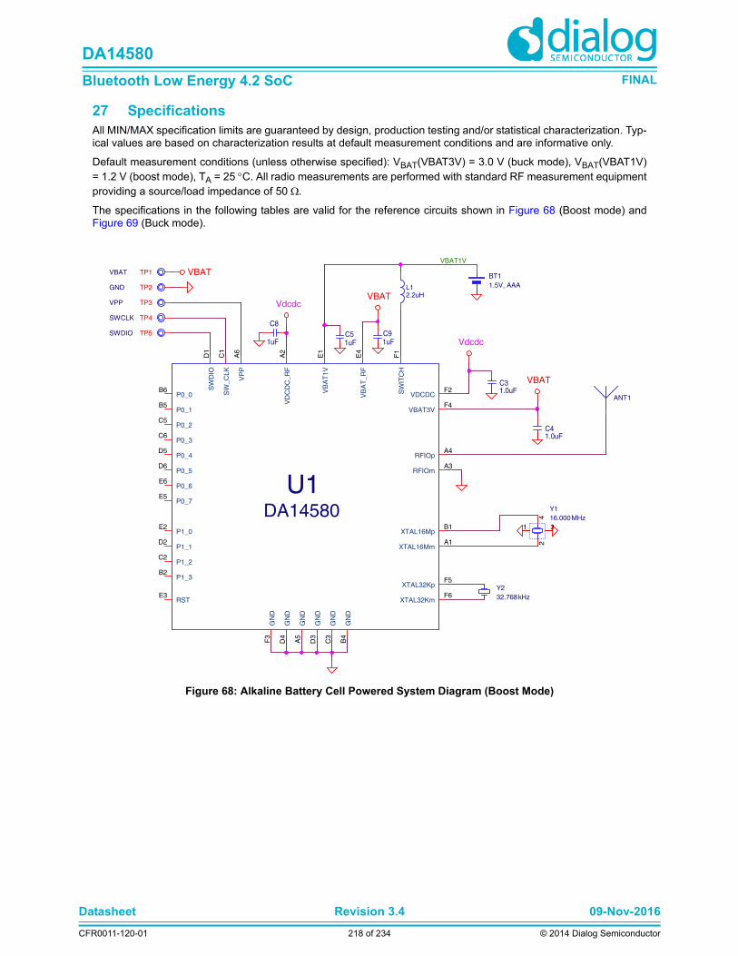
Datasheet Revision 3.4 09-Nov-2016
CFR0011-120-01 218 of 234 © 2014 Dialog Semiconductor
DA14580
Bluetooth Low Energy 4.2 SoC FINAL
27 SpecificationsAll MIN/MAX specification limits are guaranteed by design, production testing and/or statistical characterization. Typ-ical values are based on characterization results at default measurement conditions and are informative only.
Default measurement conditions (unless otherwise specified): VBAT(VBAT3V) = 3.0 V (buck mode), VBAT(VBAT1V)= 1.2 V (boost mode), TA = 25 C. All radio measurements are performed with standard RF measurement equipmentproviding a source/load impedance of 50 .
The specifications in the following tables are valid for the reference circuits shown in Figure 68 (Boost mode) andFigure 69 (Buck mode).
Figure 68: Alkaline Battery Cell Powered System Diagram (Boost Mode)

Datasheet Revision 3.4 09-Nov-2016
CFR0011-120-01 219 of 234 © 2014 Dialog Semiconductor
DA14580
Bluetooth Low Energy 4.2 SoC FINAL
Figure 69: Lithium Coin Cell Powered System Diagram (Buck Mode)

Datasheet Revision 3.4 09-Nov-2016
CFR0011-120-01 220 of 234 © 2014 Dialog Semiconductor
DA14580
Bluetooth Low Energy 4.2 SoC FINAL
Table 326: Absolute Maximum Ratings
Parameter Description Conditions Min Typ Max Unit
VPIN(LIM)(default)
limiting voltage on a pin Voltage between pin and GND (Note 23)
-0.1 min{3.6, VBAT_RF
+0.2}
V
TSTG storage temperature -50 150 °C
tR(SUP) supply rise time Power supply rise time 100 ms
VBAT(LIM)(VBAT1V)
limiting battery supply voltage
Supply voltage on VBAT1V in a boost con-verter application (VBAT3V is second out-put of boost-converter in this case)(Note 23)
-0.1 3.6 V
VBAT(LIM)(VBAT3V)
limiting battery supply voltage
Supply voltage on VBAT3V and VBAT_RF in a buck-converter application, pin VBAT1V is connected to ground(Note 23)
-0.1 3.6 V
VPIN(LIM)(1V2) limiting voltage on a pin XTAL32Km, XTAL16Mp, XTAL16Mm (Note 23)
-0.2 min(1.2,VBAT_RF+
0.2)
V
VPIN(LIM)(VDCDC_RF)
limiting voltage on the VDCDC_RF pin
Supply voltage on VDCDC_RF(Note 23)
-0.2 min(3.3,VBAT_RF+
0.2)
V
VPIN(LIM)(XTAL32Kp)
limiting voltage on a pin XTAL32Kp -0.2 min(1.5,VBAT_RF+
0.2)
V
VESD(HBM)(WLCSP34)
electrostatic discharge voltage (Human Body Model)
2000 V
VESD(HBM)(QFN40)
electrostatic discharge voltage (Human Body Model)
4000 V
VESD(HBM)(QFN48)
electrostatic discharge voltage (Human Body Model)
4000 V
VESD(MM)(WLCSP34)
electrostatic discharge voltage (Machine Model)
200 V
VESD(MM)(QFN40)
electrostatic discharge voltage (Machine Model)
200 V
VESD(MM)(QFN48)
electrostatic discharge voltage (Machine Model)
200 V
VESD(CDM)(WLCSP34)
electrostatic discharge voltage (Charged Device Model)
500 V
VESD(CDM)(QFN40)
electrostatic discharge voltage (Charged Device Model)
1000 V
VESD(CDM)(QFN48)
electrostatic discharge voltage (Charged Device Model)
1000 V

Datasheet Revision 3.4 09-Nov-2016
CFR0011-120-01 221 of 234 © 2014 Dialog Semiconductor
DA14580
Bluetooth Low Energy 4.2 SoC FINAL
Note 23: The device should not be exposed for prolonged periods of time to voltages between the Recommended Operating Conditions and the
Absolute Maximum Ratings range.
Note 24: Cold boot should not be performed if voltage is less than 2.5 V because of possible corruption during OTP data mirroring. Trim values pro-
grammed in the OTP as well as the application image, should be copied into RAM while VBAT3V >= 2.5 V.
Table 327: Recommended Operating Conditions
Parameter Description Conditions Min Typ Max Unit
VPP programming voltage Supply voltage on pin VPP during OTP pro-gramming; TJ 50 C
6.6 6.7 6.8 V
VBAT(VBAT1V) battery supply voltage Supply voltage on VBAT1V in a boost con-verter application (VBAT3V is second out-put of boost-converter in this case)
0.9 3.3 V
VBAT(VBAT3V) battery supply voltage Supply voltage on VBAT3V and VBAT_RF in a buck-converter application, pin VBAT1V is connected to ground
2.35(Note 24)
3.3 V
VPIN(default) voltage on a pin Voltage between pin and GND
0 min(3.3,VBAT_RF+
0.2)
V
VPIN(1V2) voltage on a pin XTAL32Km, XTAL16Mp, XTAL16Mm
0 1.2 V
VPIN(VDCDC_RF)
voltage on a pin Supply voltage on VDCDC_RF
0 3.3 V
TA ambient temperature -40 85 °C
Table 328: DC Characteristics
Parameter Description Conditions Min Typ Max Unit
IBAT(DP_SLP)_BOOST_1kB
battery supply current Boost configuration in deep-sleep with 1 kB retention RAM active, running from RC32K oscillator at lowest fre-quency
0.48 A
IBAT(DP_SLP)_BOOST_2kB
battery supply current Boost configuration in deep-sleep with 2 kB retention RAM active, running from XTAL32K oscillator
0.55 A
IBAT(DP_SLP)_BOOST_8kB
battery supply current Typical boost-applica-tion in deep-sleep with 8 kB retention RAM active, running from XTAL32K oscillator
0.7 2 A
IBAT(EXT_SLP)_BOOST_43KB
battery supply current Typical boost-applica-tion in extended-sleep mode with 42 kB (Sys-RAM) and 1 kB (RetRAM) retained
1.37 A

Datasheet Revision 3.4 09-Nov-2016
CFR0011-120-01 222 of 234 © 2014 Dialog Semiconductor
DA14580
Bluetooth Low Energy 4.2 SoC FINAL
IBAT(EXT_SLP)_BOOST_50kB
battery supply current Typical boost-applica-tion in extended-sleep mode with 42 kB (Sys-RAM) and 8 kB (RetRAM) retained
1.5 3 A
IBAT(DP_SLP)_BUCK_1kB
battery supply current Buck configuration in deep-sleep with 1 kB retention RAM active, running from RC32K oscillator at lowest fre-quency
0.4 A
IBAT(DP_SLP)_BUCK_2kB
battery supply current Buck configuration in deep-sleep with 2 kB retention RAM active, running from XTAL32K oscillator
0.45 A
IBAT(DP_SLP)_BUCK_8kB
battery supply current Typical buck-application in deep-sleep with 8 kB retention RAM active, running from XTAL32K oscillator
0.6 2 A
IBAT(EXT_SLP)_BUCK_43KB
battery supply current Typical buck-application in extended-sleep mode with 42 kB (SysRAM) and 1 kB (RetRAM) retained
1.2 A
IBAT(EXT_SLP)_BUCK_50kB
battery supply current Typical buck-application in extended-sleep mode with 42 kB (SysRAM) and 8 kB (RetRAM) retained
1.4 3 A
IBAT(ACT_RX)_BOOST
battery supply current Typical application with boost converter and receiver active
13.4 16 mA
IBAT(ACT_TX)_BOOST
battery supply current Typical application with boost converter and transmitter active
12.4 15 mA
IBAT(ACT_RX)_BUCK
battery supply current Typical application with buck converter and receiver active
5.1 6 mA
IBAT(ACT_TX)_BUCK
battery supply current Typical application with buck converter and transmitter active
4.8 6 mA
Table 329: Timing Characteristics
Parameter Description Conditions Min Typ Max Unit
tSTA(BOOST) startup time Boost-mode; time from deep-sleep to software start.Typical application, run-ning from retention RAM on 16 MHz RC oscillator
1.2(Note 25)
ms
Table 328: DC Characteristics
Parameter Description Conditions Min Typ Max Unit

Datasheet Revision 3.4 09-Nov-2016
CFR0011-120-01 223 of 234 © 2014 Dialog Semiconductor
DA14580
Bluetooth Low Energy 4.2 SoC FINAL
Note 25: Worst-case value under Normal Operating Conditions.
Note 26: Using the internal varicaps a wide range of crystals can be trimmed to the required tolerance.
Note 27: Maximum allowed frequency tolerance for compensation by the internal varicap trimming mechanism.
Note 28: Select a crystal which can handle a drive-level equal or more than this specification
tSTA(BUCK) startup time Buck-mode; time from deep-sleep to software start.Typical application, run-ning from retention RAM on 16 MHz RC oscillator
1(Note 25)
ms
Table 329: Timing Characteristics
Parameter Description Conditions Min Typ Max Unit
Table 330: 16 MHz Crystal Oscillator: Recommended Operating Conditions
Parameter Description Conditions Min Typ Max Unit
fXTAL(16M) crystal oscillator fre-quency
16 MHz
ESR(16M) equivalent series resis-tance
100
CL(16M) load capacitance No external capacitors are required
10 12 pF
C0(16M) shunt capacitance 5 pF
fXTAL(16M) crystal frequency toler-ance
After optional trimming; including aging and tem-perature drift(Note 26)
-20 20 ppm
fX-
TAL(16M)UNTcrystal frequency toler-ance
Untrimmed; including aging and temperature drift(Note 27)
-40 40 ppm
PDRV(MAX)(16M)
maximum drive power (Note 28) 100 W
VCLK(EXT)(16M) external clock voltage Only in case of an exter-nal reference clock on XTAL16Mp (XTAL16Mm floating or connected to mid-level 0.6 V)
1 1.2 V
N(EXTER-NAL)16M
phase noise fC = 50 kHzin case of an external reference clock
-130 dBc/Hz
Table 331: 16 MHz Crystal Oscillator: Timing Characteristics
Parameter Description Conditions Min Typ Max Unit
tSTA(XTAL)(16M) crystal oscillator startup time
0.5 2 3 ms

Datasheet Revision 3.4 09-Nov-2016
CFR0011-120-01 224 of 234 © 2014 Dialog Semiconductor
DA14580
Bluetooth Low Energy 4.2 SoC FINAL
Note 29: Select a crystal that can handle a drive-level of at least this specification.
Note 30: This parameter is very much dependent on crystal parameters
Note 31: A low value will result in lowest power consumption, keep this value at 1 uF or 2 uF.
Table 332: 32 kHz Crystal Oscillator: Recommended Operating Conditions
Parameter Description Conditions Min Typ Max Unit
VCLK(EXT)(32K) external clock voltage peak-peak voltage of external clock at XTAL32Kp, pin XTAL32Km floating.note: XTAL32Kp is inter-nally AC coupled
0.1 0.2 1.5 V
fXTAL(32k) crystal oscillator fre-quency
frequency range for an external clock(for a crystal, use either 32.000 kHz or 32.768 kHz)
10 32.768 100 kHz
ESR(32k) equivalent series resis-tance
100 k
CL(32k) load capacitance no external capacitors are required for a 6 pF or 7 pF crystal
6 7 9 pF
C0(32k) shunt capacitance 1 2 pF
fXTAL(32k) crystal frequency toler-ance (including aging)
Timing accuracy is domi-nated by crystal accu-racy. A much smaller value is preferred
-250 250 ppm
PDRV(MAX)(32k) maximum drive power (Note 29) 0.1 W
Table 333: 32 kHz Crystal Oscillator: Timing Characteristics
Parameter Description Conditions Min Typ Max Unit
tSTA(XTAL)(32k) crystal oscillator startup time
Typical application, time until 1000 clocks are detected(Note 30)
0.4 s
Table 334: DC-DC Converter: Recommended Operating Conditions
Parameter Description Conditions Min Typ Max Unit
L effective inductance 1.5 2.2 3 H
COUT(VDCDC) effective load capaci-tance
VDCDC and VDDCRF combined(Note 31)
0.5 1 10 F
COUT(VBAT3V) effective load capaci-tance
VBATRF and VBAT3V combined are the sec-ond output of the boost-converter(Note 31)
0.5 1 10 F
Table 335: DC-DC Converter: DC Characteristics
Parameter Description Conditions Min Typ Max Unit
VO(BUCK) output voltage default settings 1.41 V
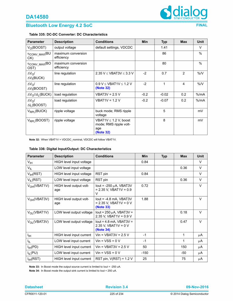
Datasheet Revision 3.4 09-Nov-2016
CFR0011-120-01 225 of 234 © 2014 Dialog Semiconductor
DA14580
Bluetooth Low Energy 4.2 SoC FINAL
Note 32: When VBAT1V > VDCDC_nominal, VDCDC will follow VBAT1V.
Note 33: In Boost mode the output source current is limited to Iout = -250 uA.
Note 34: In Boost mode the output sink current is limited to Iout = 250 uA.
VO(BOOST) output voltage default settings, VDCDC 1.41 V
CONV_MAX(BUCK)
maximum conversion efficiency
86 %
CONV_MAX(BOOST)
maximum conversion efficiency
80 %
VO/VI(BUCK)
line regulation 2.35 V VBAT3V 3.3 V -2 0.7 2 %/V
VO/VI(BOOST)
line regulation 0.9 V VBAT1V 1.2 V(Note 32)
-2 1 4 %/V
VO/IL(BUCK) load regulation VBAT3V = 2.5 V -0.2 -0.02 0.2 %/mA
VO/IL(BOOST)
load regulation VBAT1V = 1.2 V -0.2 -0.07 0.2 %/mA
VRPL(BUCK) ripple voltage buck mode; RMS ripple voltage
5 mV
VRPL(BOOST) ripple voltage VBAT1V 1.2 V, boost mode; RMS ripple volt-age(Note 32)
8 mV
Table 335: DC-DC Converter: DC Characteristics
Parameter Description Conditions Min Typ Max Unit
Table 336: Digital Input/Output: DC Characteristics
Parameter Description Conditions Min Typ Max Unit
VIH HIGH level input voltage 0.84 V
VIL LOW level input voltage 0.36 V
VIH(RST) HIGH level input voltage RST pin 0.84 V
VIL(RST) LOW level input voltage RST pin 0.36 V
VOH(VBAT1V) HIGH level output volt-age
Iout = -250 A, VBAT3V = 2.35 V, VBAT1V = 0.9 V
0.72 V
VOH(VBAT3V) HIGH level output volt-age
Iout = -4.8 mA, VBAT3V = 2.35 V, VBAT1V = 0 V (Note 33)
1.88 V
VOL(VBAT1V) LOW level output voltage Iout = 250 A, VBAT3V = 2.35 V, VBAT1V = 0.9 V
0.18 V
VOL(VBAT3V) LOW level output voltage Iout = 4.8 mA, VBAT3V = 2.35 V, VBAT1V = 0 V (Note 34)
0.47 V
IIH HIGH level input current Vin = VBAT3V = 2.5 V -1 1 A
IIL LOW level input current Vin = VSS = 0 V -1 1 A
IIH(PD) HIGH level input current Vin = VBAT3V = 2.5 V 50 150 A
IIL(PU) LOW level input current Vin = VSS = 0 V -150 -50 A
IIH(RST) HIGH level input current RST pin, V(RST) = 1.2 V 25 75 A

Datasheet Revision 3.4 09-Nov-2016
CFR0011-120-01 226 of 234 © 2014 Dialog Semiconductor
DA14580
Bluetooth Low Energy 4.2 SoC FINAL
Note 35: The DCDC-converter efficiency is assumed to be 100 % to enable benchmarking of the radio currents at battery supply domain (VBAT3V =
3 V).
Table 337: General Purpose ADC: Recommended Operating Conditions
Parameter Description Conditions Min Typ Max Unit
NBIT(ADC) number of bits (resolu-tion)
10 bit
Table 338: General Purpose ADC: DC Characteristics
Parameter Description Conditions Min Typ Max Unit
VI(ZS) zero-scale input voltage single-ended, calibrated at zero input
-2.5 0 2.5 mV
VI(FS) full-scale input voltage single-ended, calibrated at zero input
1150 1180 1250 mV
VI(FSN) negative full-scale input voltage
differential, calibrated at zero input
-1180 mV
VI(FSP) positive full-scale input voltage
differential, calibrated at zero input
1180 mV
INL integral non-linearity -2 2 LSB
DNL differential non-linearity -2 2 LSB
Table 339: General Purpose ADC: Timing Characteristics
Parameter Description Conditions Min Typ Max Unit
tCONV(ADC) conversion time Excluding initial settling time of the LDO and the 3x-attenuation (if used):
LDO settling time is 20 s (max), 3x-attenuation settling time = 1 s (max)Using internal ADC-clock (~200 MHz)
0.25 0.4 s
Table 340: Radio: DC Characteristics
Parameter Description Conditions Min Typ Max Unit
IBAT(RF)RX battery supply current receive mode; radio receiver and synthesizer active; DCDC converter assumed ideal; TA = 25 °C(Note 35)
3.7 4.3 mA
IBAT(RF)TX battery supply current transmit mode; radio transmitter and synthe-sizer active; DCDC con-verter assumed ideal; TA = 25 °C(Note 35)
3.4 4 mA
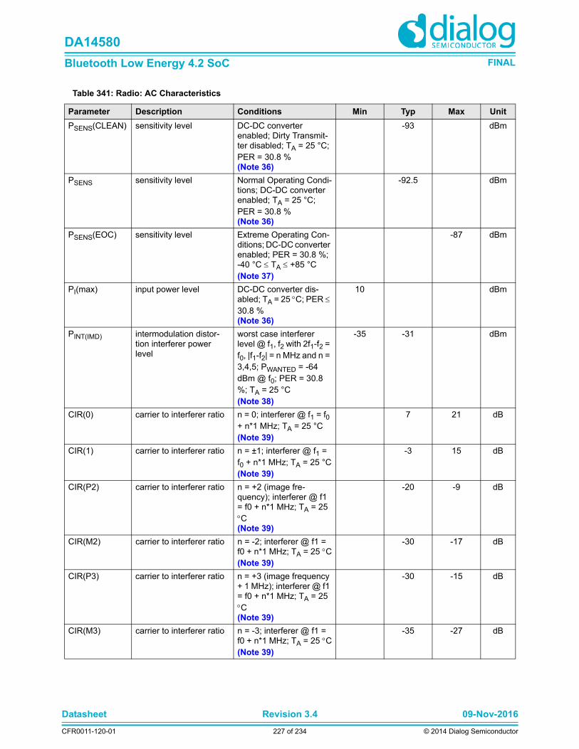
Datasheet Revision 3.4 09-Nov-2016
CFR0011-120-01 227 of 234 © 2014 Dialog Semiconductor
DA14580
Bluetooth Low Energy 4.2 SoC FINAL
Table 341: Radio: AC Characteristics
Parameter Description Conditions Min Typ Max Unit
PSENS(CLEAN) sensitivity level DC-DC converter enabled; Dirty Transmit-ter disabled; TA = 25 °C; PER = 30.8 %(Note 36)
-93 dBm
PSENS sensitivity level Normal Operating Condi-tions; DC-DC converter enabled; TA = 25 °C; PER = 30.8 %(Note 36)
-92.5 dBm
PSENS(EOC) sensitivity level Extreme Operating Con-ditions; DC-DC converter enabled; PER = 30.8 %; -40 °C TA +85 °C(Note 37)
-87 dBm
PI(max) input power level DC-DC converter dis-abled; TA = 25 C; PER 30.8 %(Note 36)
10 dBm
PINT(IMD) intermodulation distor-tion interferer power level
worst case interferer level @ f1, f2 with 2f1-f2 = f0, |f1-f2| = n MHz and n = 3,4,5; PWANTED = -64 dBm @ f0; PER = 30.8 %; TA = 25 °C (Note 38)
-35 -31 dBm
CIR(0) carrier to interferer ratio n = 0; interferer @ f1 = f0 + n*1 MHz; TA = 25 °C(Note 39)
7 21 dB
CIR(1) carrier to interferer ratio n = ±1; interferer @ f1 = f0 + n*1 MHz; TA = 25 °C(Note 39)
-3 15 dB
CIR(P2) carrier to interferer ratio n = +2 (image fre-quency); interferer @ f1 = f0 + n*1 MHz; TA = 25 C(Note 39)
-20 -9 dB
CIR(M2) carrier to interferer ratio n = -2; interferer @ f1 = f0 + n*1 MHz; TA = 25 C(Note 39)
-30 -17 dB
CIR(P3) carrier to interferer ratio n = +3 (image frequency + 1 MHz); interferer @ f1 = f0 + n*1 MHz; TA = 25 C(Note 39)
-30 -15 dB
CIR(M3) carrier to interferer ratio n = -3; interferer @ f1 = f0 + n*1 MHz; TA = 25 C(Note 39)
-35 -27 dB

Datasheet Revision 3.4 09-Nov-2016
CFR0011-120-01 228 of 234 © 2014 Dialog Semiconductor
DA14580
Bluetooth Low Energy 4.2 SoC FINAL
CIR(4) carrier to interferer ratio |n| >= 4 (any other BLE channel); interferer @ f1 = f0 + n*1 MHz; TA = 25 °C(Note 39)
-37 -27 dB
PBL(I) blocker power level 30 MHz fBL 2000 MHz; PWANTED = -67 dBm; TA = 25 °C(Note 40)
-5 dBm
PBL(II) blocker power level 2003 MHz fBL 2399 MHz; PWANTED = -67 dBm; TA = 25 °C(Note 40)
-15 dBm
PBL(III) blocker power level 2484 MHz fBL 2997 MHz; PWANTED = -67 dBm; TA = 25 C(Note 40)
-15 dBm
PBL(IV) blocker power level 3000 MHz fBL 12.75 GHz; PWANTED = -67 dBm; TA = 25 C(Note 40)
-5 dBm
PRSSI(min) RSSI power level absolute power level for RXRSSI[7:0] = 0; TA = 25 °C(Note 41)
-115 -112 -109 dBm
PRSSI(max) RSSI power level upper limit of monoto-nous range; TA = 25 °C
-26 -19 dBm
LACC(RSSI)BOOST
level accuracy tolerance of 5 % to 95 % confidence interval of PRF: when RXRSSI[7:0] = X, 50 < X < 175; burst mode 1500 packets; TA = 25 °C; DC-DC con-verter in BOOST mode
0 3 dB
LACC(RSSI)BUCK
level accuracy tolerance of 5 % to 95 % confidence interval of PRF: when RXRSSI[7:0] = X, 50 < X < 175; burst mode 1500 packets; TA = 25 °C; DC-DC con-verter in BUCK mode
0 2 dB
LRES(RSSI) level resolution gradient of monotonous range for RXRSSI[7:0] = X, 50 < X < 175; burst mode 1500 packets; TA = 25C
0.46 0.474 0.485 dB/LSB
ACP(2M) adjacent channel power level
fOFFSET = 2 MHz; TA = 25C(Note 42)
-53 -50 dBm
Table 341: Radio: AC Characteristics
Parameter Description Conditions Min Typ Max Unit

Datasheet Revision 3.4 09-Nov-2016
CFR0011-120-01 229 of 234 © 2014 Dialog Semiconductor
DA14580
Bluetooth Low Energy 4.2 SoC FINAL
Note 36: Measured according to Bluetooth® Low Energy Test Specification RF-PHY.TS/4.0.1, section 6.4.1.
Note 37: Measured according to Bluetooth® Low Energy Test Specification RF-PHY.TS/4.0.1, section 6.4.2.
Note 38: Measured according to Bluetooth® Core Technical Specification document, version 4.2, volume 6, section 4.4. Published value is for n =
IXIT = 4 . IXIT = 5 gives the same results, IXIT = 3 gives results that are 5 dB lower.
Note 39: Measured according to Bluetooth® Core Technical Specification document, version 4.2, volume 6, section 4.2.
Note 40: Measured according to Bluetooth® Core Technical Specification document, version 4.2, volume 6, section 4.3. Due to limitations of the
measurement equipment, levels of -5 dBm should be interpreted as > -5 dBm.
Note 41: PRF = PRSSI(min) + LRES(RSSI) x RXRSSI[7:0] ± LACC(RSSI). Thanks to constant gain biasing of RF part in the receiver, the RSSI can
be used to estimate absolute power levels, rather than mere level changes. Even across the full temperature range the variation is limited.
Note 42: Measured according to Bluetooth® Low Energy Test Specification RF-PHY.TS/4.0.1, section 6.2.3.
Note 43: To activate the "Near Field Mode", program address 0x50002418 with the value 0x0030.
Note 44: Maximum recommended connection interval (including slave latency) for the RCX usage is 2 s.
ACP(2M)(EOC) adjacent channel power level
fOFFSET = 2 MHz; -40C TA +85C(Note 42)
-53 -47 dBm
ACP(3M) adjacent channel power level
fOFFSET 3 MHz; TA = 25C(Note 42)
-57 -55 dBm
ACP(3M)(EOC) adjacent channel power level
fOFFSET 3 MHz; -40C TA +85C(Note 42)
-57 -47 dBm
PO output power level VDD = 3 V; maximum gain; TA = 25 °C
-2 -1 0 dBm
PO(HD2) output power level (sec-ond harmonic)
VDD = 3 V; maximum gain; TA = 25 C
-54 -40 dBm
PO(HD3) output power level (third harmonic)
VDD = 3 V; maximum gain; TA = 25 C
-56 -40 dBm
PO(HD4) output power level (fourth harmonic)
VDD = 3 V; maximum gain; TA = 25 C
-70 -40 dBm
PO(HD5) output power level (fifth harmonic)
VDD = 3 V; maximum gain; TA = 25 C
-70 -40 dBm
PO(NFM) output power level in 'Near Field Mode'
VDD = 3 V; maximum gain; TA = 25 °C(Note 43)
-25 -20 -15 dBm
Table 341: Radio: AC Characteristics
Parameter Description Conditions Min Typ Max Unit
Table 342: Stable Low Frequency RCX Oscillator: Timing Characteristics
Parameter Description Conditions Min Typ Max Unit
fRC(RCX) RCX oscillator frequency default setting, buck mode only
5 10 40 kHz
fRC(RCX) RCX oscillator fre-quency drift
buck mode only (Note 44)
-500 500 ppm
TA/t(RCX)100ms
ambient temperature gradient
buck mode only; connec-tion interval 100 ms
0.66 °C/s
TA/t(RCX)4s ambient temperature gradient
buck mode only; connec-tion interval 4 s
0.33 °C/s

Datasheet Revision 3.4 09-Nov-2016
CFR0011-120-01 230 of 234 © 2014 Dialog Semiconductor
DA14580
Bluetooth Low Energy 4.2 SoC FINAL
28 Package Information
28.1 MOISTURE SENSITIVITY LEVEL (MSL)
The MSL is an indicator for the maximum allowabletime period (floor life time) in which a moisture sensi-tive plastic device, once removed from the dry bag, canbe exposed to an environment with a maximum tem-perature of 30 °C and a maximum relative humidity of60 % RH. before the solder reflow process.
WLCSP packages are qualified for MSL 1. QFN packages are qualified for MSL 3.
28.2 WLCSP HANDLING
Manual handling of WLCSP packages should bereduced to the absolute minimum. In cases where it isstill necessary, a vacuum pick-up tool should be used.In extreme cases plastic tweezers could be used, butmetal tweezers are not acceptable, since contact mayeasily damage the silicon chip.Removal will cause damage to the solder balls andtherefore a removed sample cannot be reused.
WLCSP is sensitive to visible and infrared light. Pre-cautions should be taken to properly shield the chip inthe final product.
28.3 SOLDERING INFORMATION
Refer to the JEDEC standard J-STD-020 for relevantsoldering information.This document can be downloaded from http://www.jedec.org
MSL Level Floor Life Time
MSL 4 72 hours
MSL 3 168 hours
MSL 2A 4 weeks
MSL 2 1 year
MSL 1 Unlimited at 30 °C / 85 % RH

Datasheet Revision 3.4 09-Nov-2016
CFR0011-120-01 231 of 234 © 2014 Dialog Semiconductor
DA14580
Bluetooth Low Energy 4.2 SoC FINAL
28.4 PACKAGE OUTLINES
Figure 70: QFN48 Package Outline Drawing

Datasheet Revision 3.4 09-Nov-2016
CFR0011-120-01 232 of 234 © 2014 Dialog Semiconductor
DA14580
Bluetooth Low Energy 4.2 SoC FINAL
Figure 71: QFN40 Package Outline Drawing

Datasheet Revision 3.4 09-Nov-2016
CFR0011-120-01 233 of 234 © 2014 Dialog Semiconductor
DA14580
Bluetooth Low Energy 4.2 SoC FINAL
Figure 72: WLCSP34 Package Outline Drawing

United Kingdom (Headquarters)Dialog Semiconductor (UK) LTDPhone: +44 1793 757700
GermanyDialog Semiconductor GmbHPhone: +49 7021 805-0
The NetherlandsDialog Semiconductor B.V.Phone: +31 73 640 8822
Email:[email protected]
Contacting Dialog SemiconductorNorth AmericaDialog Semiconductor Inc.Phone: +1 408 845 8500
JapanDialog Semiconductor K. K.Phone: +81 3 5425 4567
TaiwanDialog Semiconductor TaiwanPhone: +886 281 786 222
Web site:www.dialog-semiconductor.com
SingaporeDialog Semiconductor SingaporePhone: +65 64 8499 29
Hong KongDialog Semiconductor Hong KongPhone: +852 3769 5200
KoreaDialog Semiconductor KoreaPhone: +82 2 3469 8200
Datasheet Revision 3.4 09-Nov-2016
CFR0011-120-01 234 of 234 © 2014 Dialog Semiconductor
DA14580
Bluetooth Low Energy 4.2 SoC FINAL
China (Shenzhen)Dialog Semiconductor ChinaPhone: +86 755 2981 3669
China (Shanghai)Dialog Semiconductor ChinaPhone: +86 21 5424 9058
234
Status Definitions
Disclaimer
Information in this document is believed to be accurate and reliable. However, Dialog Semiconductor does not give any representations or warranties, expressed or implied, as to the accuracy or completeness of such information. Dialog Semi-conductor furthermore takes no responsibility whatsoever for the content in this document if provided by any information source outside of Dialog Semiconductor.
Dialog Semiconductor reserves the right to change without notice the information published in this document, including without limitation the specification and design of the related semiconductor products, software and applications.
Applications, software, and semiconductor products described in this document are for illustrative purposes only. Dialog Semiconductor makes no representation or warranty that such applications, software and semiconductor products will be suitable for the specified use without further testing or modification. Unless otherwise agreed in writing, such testing or modification is the sole responsibility of the customer and Dialog Semiconductor excludes all liability in this respect.
Customer notes that nothing in this document may be construed as a license for customer to use the Dialog Semi-conduc-tor products, software and applications referred to in this document. Such license must be separately sought by customer with Dialog Semiconductor.
All use of Dialog Semiconductor products, software and applications referred to in this document are subject to Dialog Semiconductor's Standard Terms and Conditions of Sale, available on the company website (www.dialog-semiconduc-tor.com) unless otherwise stated.
Dialog and the Dialog logo are trademarks of Dialog Semiconductor plc or its subsidiaries. All other product or service names are the property of their respective owners.
© 2014 Dialog Semiconductor. All rights reserved.
RoHS Compliance
Dialog Semiconductor's suppliers certify that its products are in compliance with the requirements of Directive 2011/65/EU of the European Parliament on the restriction of the use of certain hazardous substances in electrical and electronic equip-ment. RoHS certificates from our suppliers are available on request.
Version Datasheet Status Product Status Definition
1.<n> Target Development This datasheet contains the design specifications for product development. Specifications may change in any manner without notice.
2.<n> Preliminary Qualification This datasheet contains the specifications and preliminary char-acterization data for products in pre-production. Specifications may be changed at any time without notice in order to improve the design.
3.<n> Final Production This datasheet contains the final specifications for products in volume production. The specifications may be changed at any time in order to improve the design, manufacturing and supply. Major specification changes are communicated via Customer Product Notifications. Datasheet changes are communicated via www.dialog-semiconductor.com.
4.<n> Obsolete Archived This datasheet contains the specifications for discontinued products. The information is provided for reference only.

Mouser Electronics
Authorized Distributor
Click to View Pricing, Inventory, Delivery & Lifecycle Information: Dialog Semiconductor:
DA14580DONGLE DA14580PRODTLKT