d/a converter cellular automaton architecturedownloads.hindawi.com/journals/vlsi/1998/091849.pdf ·...
TRANSCRIPT

VLSI DESIGN1998, Vol. 7, No. 2, pp. 203-210Reprints available directly from the publisherPhotocopying permitted by license only
(C) 1998 OPA (Overseas Publishers Association)Amsterdam B.V. Published under license
under the Gordon and Breach SciencePublishers imprint.
Printed in India.
A Stochastic D/A Converter Based on a CellularAutomaton Architecture
I. ANDREADIS*, I. KOKOLAKIS, A. GASTERATOS and PH. TSALIDES
Laboratory of Electronics, Section of Electronics and Information Systems Technology,Department of Electrical and Computer Engineering, Democritus University of Thrace 67100 Xanthi, Greece
(Received 22 February 1997)
The design and VLSI implementation of a new stochastic D/A converter using theproperties of Cellular Automata (CA) is presented in this paper. The converter isimplemented using a Double Layer Metal (DLM), 0.7 tm, N-well, CMOS technologyprocess provided by the European Silicon Structures (ES2). Its maximum conversionrate is 6 kHz and it is intended to be used in low-cost applications. Additionally, theproposed approach integrates into digital techniques more easily than other popularbuilding D/A techniques.
Keywords: Converters, cellular automata, VLSI
1. INTRODUCTION
The goal of a D/A converter is to convert aquantity specified as a binary number to a voltageor current proportional to the value of thisnumber. The most popular D/A conversiontechniques are: (i) scaled resistors into summingjunction, (ii) R-2R ladder and (iii) stochastic. Thevast majority of converters use the resistor ladderapproach. The stochastic technique though sloweris significantly lower in cost and it integrates intodigital techniques more easily [1].The key building block of a stochastic D/A is
the Pseudo Random Number Generator (PRNG).In the stochastic D/A converter approach thepseudo number generation is usually performed
*Corresponding author.
through software. Although this results in a low-cost implementation the conversion rates achievedare only a few tens Hz. The use of specifichardware (CA or LFSRs) in the pseudo numbergeneration process significantly improves conver-sion rates. PRNGs based on Additive CellularAutomata (ACA) do not have long feedback loopsand, therefore, can operate at significantly higherspeeds compared to traditional Linear FeedbackShift Register (LFSR) based PRNGs [2, 3]. A six-cell CA circuit is 1.7 times faster than theanalogous LFSR circuit. Also, they comparefavourably with the autocorrelation and crosscorrelation of LFSR generators. Furthermore,their regular structure and interconnections resultin efficient layouts and less silicon. This paper
203
204 I. ANDREADIS et al.
presents for the first time, as far as we know, thedesign and VLSI implementation of a stochasticD/A converter using the properties of CA. Itsmaximum speed of operation is 6 kHz. The D/Aconverter is intended to be used in low-cost D/Aconversion applications.
2. DEFINITIONS OF CELLULARAUTOMATA
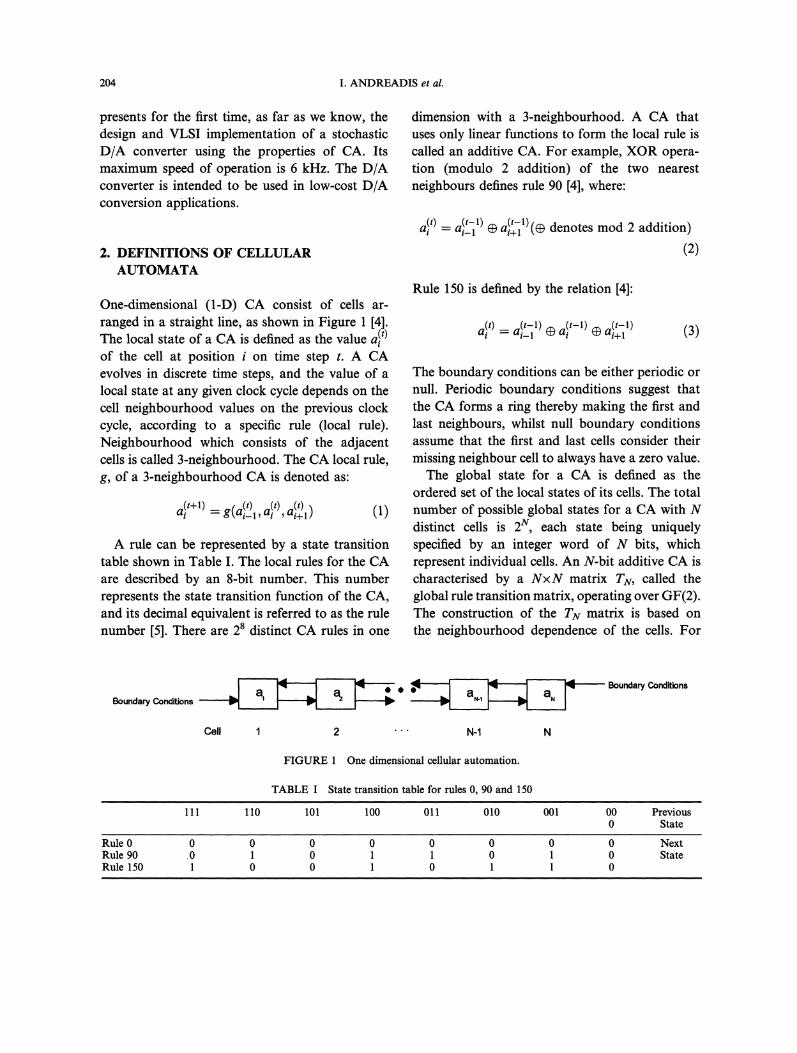
One-dimensional (l-D) CA consist of cells ar-ranged in a straight line, as shown in Figure 1 [4].The local state of a CA is defined as the value alt)
of the cell at position on time step t. A CAevolves in discrete time steps, and the value of alocal state at any given clock cycle depends on thecell neighbourhood values on the previous clockcycle, according to a specific rule (local rule).Neighbourhood which consists of the adjacentcells is called 3-neighbourhood. The CA local rule,g, of a 3-neighbourhood CA is denoted as:
(t+l) g(a}21 alt)’’(t)ai "i+ (1)
A rule can be represented by a state transitiontable shown in Table I. The local rules for the CAare described by an 8-bit number. This numberrepresents the state transition function of the CA,and its decimal equivalent is referred to as the rulenumber [5]. There are 28 distinct CA rules in one
dimension with a 3-neighbourhood. A CA thatuses only linear functions to form the local rule iscalled an additive CA. For example, XOR opera-tion (modulo 2 addition) of the two nearestneighbours defines rule 90 [4], where:
a}t) ai-l(t-1) 1 "i+l"(t--1)(@ denotes mod 2 addition)
Rule 150 is defined by the relation [4]:
a}t) a(t-1) ..(t-l) a(t-1)"i-1 ( i ] "i+1 (3)
The boundary conditions can be either periodic ornull. Periodic boundary conditions suggest thatthe CA forms a ring thereby making the first andlast neighbours, whilst null boundary conditionsassume that the first and last cells consider theirmissing neighbour cell to always have a zero value.The .global state for a CA is defined as the
ordered set of the local states of its cells. The totalnumber of possible global states for a CA with Ndistinct cells is 2v, each state being uniquelyspecified by an integer word of N bits, whichrepresent individual cells. An N-bit additive CA ischaracterised by a NxN matrix Tr, called theglobal rule transition matrix, operating over GF(2).The construction of the Tv matrix is based onthe neighbourhood dependence of the cells. For
Boundary Conditions
111
Cell 2 N-1 N
Boundary Conditions
FIGURE One dimensional cellular automation.
110
TABLE State transition table for rules 0, 90 and 150
101 100 011 010 001 00 Previous0 State
Rule 0 0 0Rule 90 .0Rule 150 0
0 0 0 0 0 0 Next0 0 0 State0 0 0
STOCHASTIC D/A CONVERTER 205
example rule 90 is characterised by the followingmatrix:
0 0 0 0. 0 0
1 0 1 0 0. 0 0
TN= 0 1 0 1 0. 0 0 (4)
0 0
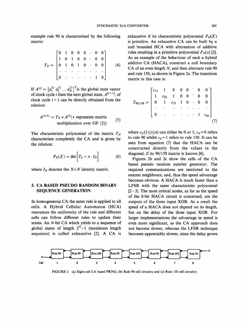
exhaustive if its characteristic polynomial PX)is primitive. An exhaustive CA can be built by anull bounded HCA with alternation of additiverules resulting in a primitive polynomial Px) [2].As an example of the behaviour of such a hybridadditive CA (HACA), construct a null boundaryCA of an even length N, and then alternate rule 90and rule 150, as shown in Figure 2a. The transitionmatrix in this case is"
If a(t) [at) at).., a?] ris the global state vectorof clock cycle then the next global state, A(t + 1), ofclock cycle + 1 can be directly obtained from therelation:
A(t+l) TN * A(t)(* represents matrix
multiplication over GF (2))
T90/150
Cll 1 0 0 0 0 0
C22 0 0 0 0
0 1 c33 0 0 0
0 Cnn
(7)
The characteristic polynomial of the matrix Tvcharacterises completely the CA and is given bythe relation:
Pv(X) det ITn +x. IN] (6)
where lv denotes the NxN identity matrix.
3. CA BASED PSEUDO RANDOM BINARYSEQUENCE GENERATION
In homogeneous CA the same rule is applied to allcells. A Hybrid Cellular Automaton (HCA)renounces the uniformity of the rule and differentcells can follow different rules to update theirstates. An N-bit CA which yields to a sequence ofglobal states of length 2v-1 (maximum lengthsequence) is called exhaustive [2]. A CA is
where cii(1 <i<n) can either be 0 or 1; ii"-" 0 refersto rule 90 whilst cii refers to rule 150. It can beseen from equation (7) that the HACA can beconstructed directly from the values in thediagonal, if its 90/150 matrix is known [6].
Figures 2b and 2c show the cells of the CAbased pseudo random number generator. Therequired communications are restricted to thenearest neighbours, and, thus the speed advantagebecomes obvious. A HACA is much faster than aLFSR with the same characteristic polynomial[2-3]. The most critical nodes, as far as the speedof the 8-bit HACA circuit is concerned, are theoutputs of the three input XOR. As a result thespeed of a HACA does not depend on its length,but on the delay of the three input XOR. Forlarger implementations the advantage in speed iseven more significant, as the CA approach doesnot become slower, whereas the LFSR techniquebecomes appreciably slower, since the delay grows
Cell 2 3
150 Rule 90 Rule 150 Rule 90 Rule 150 Rule 90
4 5 6 7 8
FIGURE 2 (a) Eight-cell CA based PRNG, (b) Rule 90 cell circuitry and (c) Rule 150 cell circuitry.
206 I. ANDREADIS et al.
Next Neighbour Next Neighbour 4. CIRCUITRY OF THE STOCHASTIC D/A
XOR
Previous Neighbour
DFLIP-FLOP
Clock
Reset
Previous Neighbour
Rule 150 Cell
The block diagram of a stochastic converter isshown in Figure 4. In this circuit, the digital valueis converted to a time ratio which is output as apulse width. The pulses are output as//max for time
Ton followed by zero for time Toff in a continu-ously repeated cycle until a new Your is required.The pulse train is then integrated by an externallossy integrator circuit. This is a classical case of asmoothing (or reconstruction) filter. The output ofthe integrator, assuming a very long time constant,is:
Next Neighbour
l XOR
Next Neighbour
DFLIP-FLOP lClock
ResetPrevious Neighbour Previous Neighbour
Rule 90 Cell
FIGURE 2 (Continued).
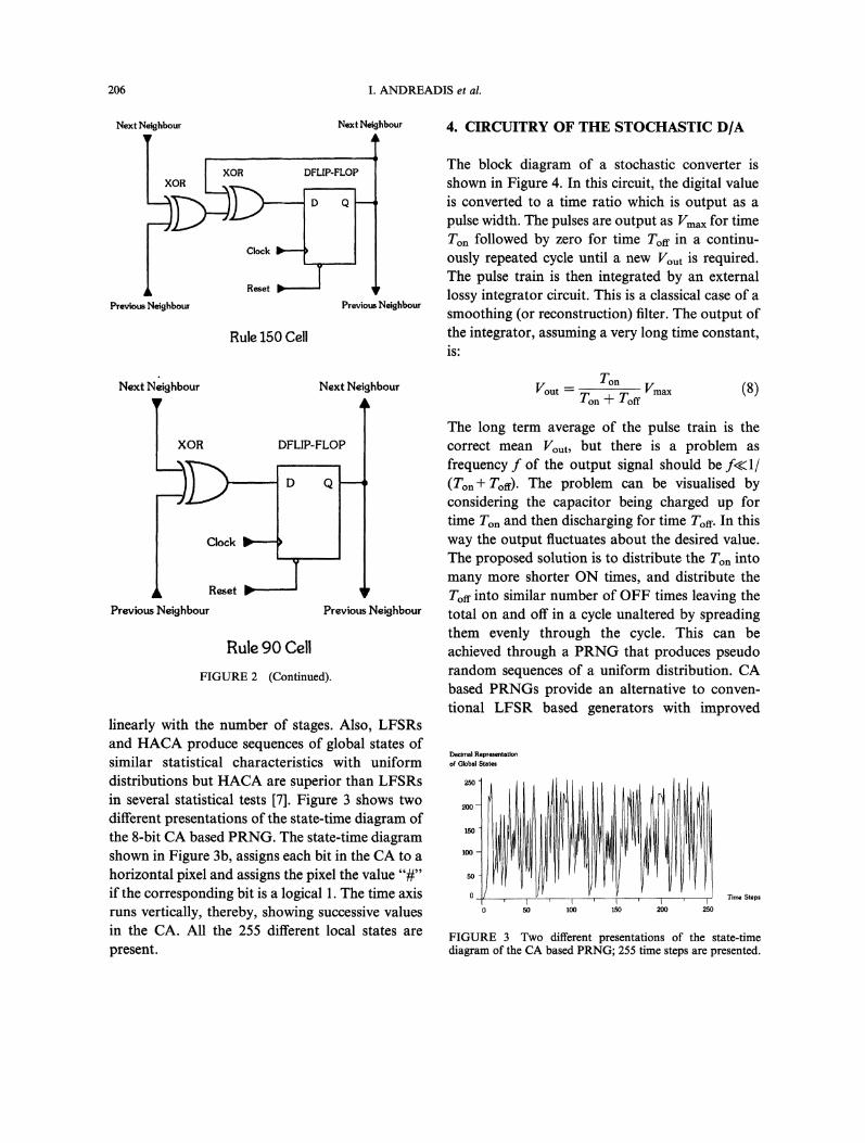
linearly with the number of stages. Also, LFSRsand HACA produce sequences of global states ofsimilar statistical characteristics with uniformdistributions but HACA are Superior than LFSRsin several statistical tests [7]. Figure 3 shows twodifferent presentations of the state-time diagram ofthe 8-bit CA based PRNG. The state-time diagramshown in Figure 3b, assigns each bit in the CA to ahorizontal pixel and assigns the pixel the value "#"if the corresponding bit is a logical 1. The time axisruns vertically, thereby, showing successive valuesin the CA. All the 255 different local states arepresent.
TonVout Vmax (8)To. + ToThe long term average of the pulse train is thecorrect mean Vout, but there is a problem asfrequency f of the output signal should be f<<l/(Ton+ Tort). The problem can be visualised byconsidering the capacitor being charged up fortime To and then discharging for time Tom In thisway the output fluctuates about the desired value.The proposed solution is to distribute the To intomany more shorter ON times, and distribute theTort into similar number of OFF times leaving thetotal on and off in a cycle unaltered by spreadingthem evenly through the cycle. This can beachieved through a PRNG that produces pseudorandom sequences of a uniform distribution. CAbased PRNGs provide an alternative to conven-tional LFSR based generators with improved
Decimal Representation
of Global States
150
,50 lOO 50 200 250
Time Steps
FIGURE 3 Two different presentations of the state-timediagram of the CA based PRNG; 255 time steps are presented.

STOCHASTIC D/A CONVERTER 207
####
##### ######## #
##_#_.###__8#_#####_#__# ## #___#####
### ### ### #__##_#### # ###
# #### ####
# ## ##___###_#m####__..#___###_# ## #___##_#_
## ##_#_##_##_..###.._#########___## ##### #
# # #_## # ###__#_####### ### ##___####_## ##__
#######
####### #__###_#....#__..#### ##__###__.
# # ## #m####_
##__..###_ ###__##_###_._# #__###_##_###_#_ _#####__
## ## # #
___###_._ # # 8##__8#8##_ __#8###8# # # # # 8#
#..#####_ #_###_..## # _____##_
.___#_##8
_####_#_###___#8# ###8##8 ### ##8###8.__#__###_
# #_###__#_#####8###8##### #
#8 ##8#_....#_
_8#....##### 8#8####_##_#### # #8# # #
#__##_##### #
# # ##__##_#_###
# 888# #8#
_#8#888#8##_#..#8# # #_8_8###_#_.##_.#_###_##_8###..8_8#_#8
88_.##_#__## #
# ## #8##_#_####
# 88_###_#__8##88#_###__
#8#
__##_._#
# # #8_#8_88_8
8# ###8 # ##___#..8#_#_##__##__#_#8_88 # #
#8_##___#####8 #888 8###_..###8#_####_##8#8 ## # #
8## # ##__##____8##_8__8### ##..#8##88
# 8#
m##_##_####
#8 ###_#_#####__######_#####__ ### ##
##_###_###_88#.._##_####_
8# # ####_#__
#888_# ### ##_#8#8__
#8#####
## # #####__#####8##### #
## ##8 # ### 8####### ###_####_#
### ##
# 88###8### ##__8#_#_### #####88# #
# ####### ####_##__# ### ## #
# 8# ## #
# ####_#8___#########
#8 ##__##__#### #8#_##_8_#
#
## #####_#_## ## ##
# #8# 88#
FIGURE 3 (Continued).
208 I. ANDREADIS et al.
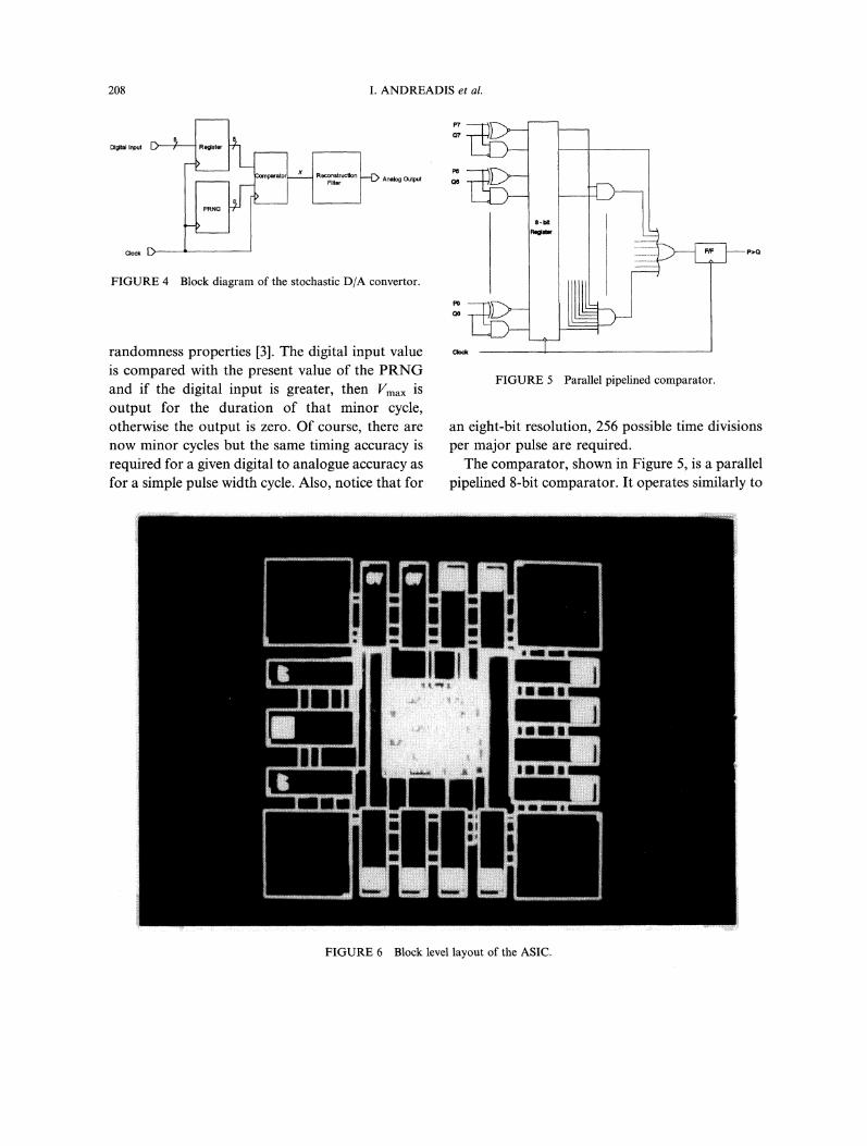
Digital Input I 8
I
Analog Output
FIGURE 4 Block diagram of the stochastic D/A convertor.
randomness properties [3]. The digital input valueis compared with the present value of the PRNGand if the digital input is greater, then Vmax isoutput for the duration of that minor cycle,otherwise the output is zero. Of course, there arenow minor cycles but the same timing accuracy isrequired for a given digital to analogue accuracy asfor a simple pulse width cycle. Also, notice that for
FIGURE 5 Parallel pipelined comparator.
an eight-bit resolution, 256 possible time divisionsper major pulse are required.The comparator, shown in Figure 5, is a parallel
pipelined 8-bit comparator. It operates similarly to
FIGURE 6 Block level layout of the ASIC.
STOCHASTIC D/A CONVERTER 209
400 800 1200 1600 2000
20--
0
400 800 1200 1600 2000
{b}
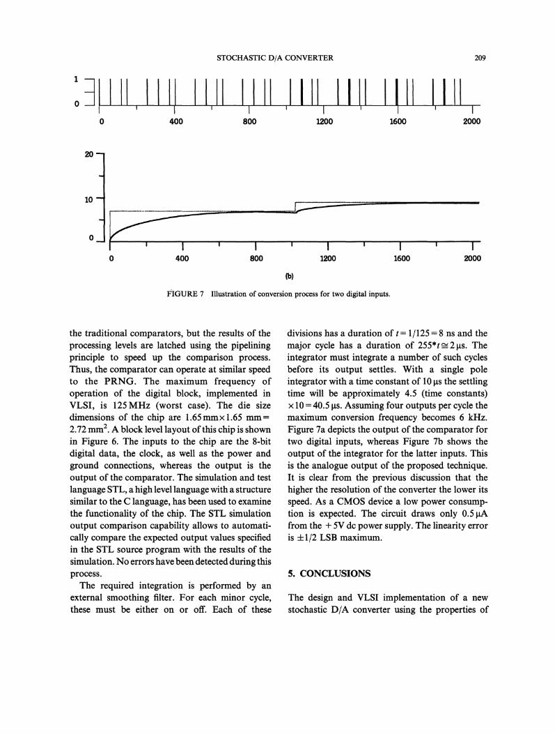
FIGURE 7 Illustration of conversion process for two digital inputs.
the traditional comparators, but the results of theprocessing levels are latched using the pipeliningprinciple to speed up the comparison process.Thus, the comparator can operate at similar speedto the PRNG. The maximum frequency ofoperation of the digital block, implemented inVLSI, is 125MHz (worst case). The die sizedimensions of the chip are 1.65 mmx 1.65 mm=2.72 mm2. A block level layout of this chip is shownin Figure 6. The inputs to the chip are the 8-bitdigital data, the clock, as well as the power andground connections, whereas the output is theoutput of the comparator. The simulation and testlanguage STL, a high level language with a structuresimilar to the C language, has been used to examinethe functionality of the chip. The STL simulationoutput comparison capability allows to automati-cally compare the expected output values specifiedin the STL source program with the results of thesimulation. No errors have been detected during thisprocess.The required integration is performed by an
external smoothing filter. For each minor cycle,these must be either on or off. Each of these
divisions has a duration of t 1/125 8 ns and themajor cycle has a duration of 255*t-2ps. Theintegrator must integrate a number of such cyclesbefore its output settles. With a single poleintegrator with a time constant of 10 ps the settlingtime will be approximately 4.5 (time constants)x 10 40.5 ts. Assuming four outputs per cycle themaximum conversion frequency becomes 6 kHz.Figure 7a depicts the output of the comparator fortwo digital inputs, whereas Figure 7b shows theoutput of the integrator for the latter inputs. Thisis the analogue output of the proposed technique.It is clear from the previous discussion that thehigher the resolution of the converter the lower itsspeed. As a CMOS device a low power consump-tion is expected. The circuit draws only 0.5 pAfrom the + 5V dc power supply. The linearity erroris 4-1/2 LSB maximum.
5. CONCLUSIONS
The design and VLSI implementation of a newstochastic D/A converter using the properties of

210 I. ANDREADIS et al.
CA have been presented in this paper. Theimplementation technique is faster than the similarexisting ones, due to the speed of the CA basedPRNG. Furthermore, it integrates more easilywith digital techniques. Its maximum frequency ofoperation is 6 kHz. The converter is intended foruse in low-cost D/A conversion applications.
Acknowledgements
The financial support of DUTH Research Com-mittee is gratefully acknowledged.
References[1] Maloberti, F. and Jonnaeum, P. O. L. (1991). "Over
Sampling Converters", (In Analogue-Digital ASICs:Circuit Techniques, Design and Applications: EditorsR.S. Soin, F. Maloberti and J. Franea), IEE Circuits andSystems Series 3.
[2] Tsalides, Ph., York, T. A. and Thanailakis, A. (July1991). "Pseudorandom Number Generators for VLSISystems Based on Linear Cellular Automata", IEEProceedings-E, 138(4), pp. 241 249.
[3] Hortensius, P., McLeod, R., Pries, W., Miller, M. andCard, H. (August 1989). "Cellular Automata-BasedPseudorandom Number Generators for Built-in-SelfTest", IEEE Trans. on CAD, 8(8), pp. 842-859.
[4] Pries, W., Thanailakis, A. and Card, H. C. (Dec. 1986)."Group Properties of Cellular Automata and VLSIApplications", IEEE Trans. on Computers, 35(12), pp.1013-1024.
[5] Wolfram, S. (1983). "Statistical Mechanics of CellularAutomata", Review of Modern Physics, 55(3), pp. 601-644.
[6] Damarla, Th. and Sathye, A. (Oct. 1993). "Applicationsof One-dimensional Cellular Automata and Linear Feed-.back Shift Registers for Pseudo-exhaustive Testing",IEEE Trans. Computer Aided Design, 12(10), pp. 1580-1591.
[7] Nandi, S. and Chaudhuri, P. P. (Jan. 1996). "Analysis ofPeriodic and Intermediate Boundary 90/150 CellularAutomata", IEEE Trans. Computers, 45(1), pp. 1-12.
Authors’ Biographies
loannis Andreadis received the Diploma Degreefrom the Department of Electrical Engineering,Democritus University of Thrace, Greece, in 1983,and the M.Sc. and Ph.D. degrees from theUniversity of Manchester Institute of Science andTechnology (UMIST), U.K., in 1985 and 1989,
respectively. His research interests are mainly inmachine vision and VLSI based computing archi-tectures for machine vision. He joined the Depart-ment of Electrical and Computer Engineering,Democritus University of Thrace, Greece, as aLecturer in 1992. He is a member of the TechnicalChamber of Greece (TEE) and the IEEE Compu-ter Society.
loannis Kokolakis received the Diploma Degreefrom the Department of Electrical and ComputerEngineering, Democritus University of Thrace,Greece, in 1993. He is currently a Ph.D. candidatein the Department of Electrical and ComputerEngineering, Democritus University of Thrace,Greece. His research interests are mainly incoding/decoding techniques using Cellular Auto-mata. He is a member of the Technical Chamberof Greece (TEE).
Antonios Gasteratos received the Diploma De-gree from the Department of Electrical andComputer Engineering, Democritus University ofThrace, Greece, in 1994. He is currently a Ph.D.candidate in the Department of Electrical andComputer Engineering, Democritus University ofThrace, Greece. His research interests are mainlyin VLSI image processing. He is a member of theTechnical Chamber of Greece (TEE).
Philippos Tsalides was born in Mirina Limnou,Greece, on October 14th 1953. He received theDiploma Degree from the University of Padova,Italy, in 1979 and the Ph.D. degree from Demo-critus University of Thrace, Greece, in 1985. He isthe Professor of Applied Electronics in theDepartment of Electrical and Computer Engineer-ing, Democritus University of Thrace, Greece. Hiscurrent research interests include VLSI architec-tures, VLSI systems, BIST Technique, Applica-tions of Cellular Automata in Image Processing,as well as in Computational Systems. He haspublished a number of papers and a Textbook onVLSI Systems (Basic Principles of Design andFabrication). He is a fellow member of the IEEand a member of the Technical Chamber ofGreece (TEE).

International Journal of
AerospaceEngineeringHindawi Publishing Corporationhttp://www.hindawi.com Volume 2010
RoboticsJournal of
Hindawi Publishing Corporationhttp://www.hindawi.com Volume 2014
Hindawi Publishing Corporationhttp://www.hindawi.com Volume 2014
Active and Passive Electronic Components
Control Scienceand Engineering
Journal of
Hindawi Publishing Corporationhttp://www.hindawi.com Volume 2014
International Journal of
RotatingMachinery
Hindawi Publishing Corporationhttp://www.hindawi.com Volume 2014
Hindawi Publishing Corporation http://www.hindawi.com
Journal ofEngineeringVolume 2014
Submit your manuscripts athttp://www.hindawi.com
VLSI Design
Hindawi Publishing Corporationhttp://www.hindawi.com Volume 2014
Hindawi Publishing Corporationhttp://www.hindawi.com Volume 2014
Shock and Vibration
Hindawi Publishing Corporationhttp://www.hindawi.com Volume 2014
Civil EngineeringAdvances in
Acoustics and VibrationAdvances in
Hindawi Publishing Corporationhttp://www.hindawi.com Volume 2014
Hindawi Publishing Corporationhttp://www.hindawi.com Volume 2014
Electrical and Computer Engineering
Journal of
Advances inOptoElectronics
Hindawi Publishing Corporation http://www.hindawi.com
Volume 2014
The Scientific World JournalHindawi Publishing Corporation http://www.hindawi.com Volume 2014
SensorsJournal of
Hindawi Publishing Corporationhttp://www.hindawi.com Volume 2014
Modelling & Simulation in EngineeringHindawi Publishing Corporation http://www.hindawi.com Volume 2014
Hindawi Publishing Corporationhttp://www.hindawi.com Volume 2014
Chemical EngineeringInternational Journal of Antennas and
Propagation
International Journal of
Hindawi Publishing Corporationhttp://www.hindawi.com Volume 2014
Hindawi Publishing Corporationhttp://www.hindawi.com Volume 2014
Navigation and Observation
International Journal of
Hindawi Publishing Corporationhttp://www.hindawi.com Volume 2014
DistributedSensor Networks
International Journal of