d75p 34 – hnc computer architecture week 4 reading and writing to ram. © c nyssen/aberdeen...
TRANSCRIPT
D75P 34 – HNC Computer Architecture
Week 4
Reading and writing to RAM.
© C Nyssen/Aberdeen College 2003All images © C Nyssen/Aberdeen College except where statedPrepared 4/9/03

Memory cells are addressable storage spaces that hold 1 byte each.
They are arranged as a rectangular matrix of individual bits. Each bit consists of a capacitor and a transistor.
The address is found by selecting the correct row and column.
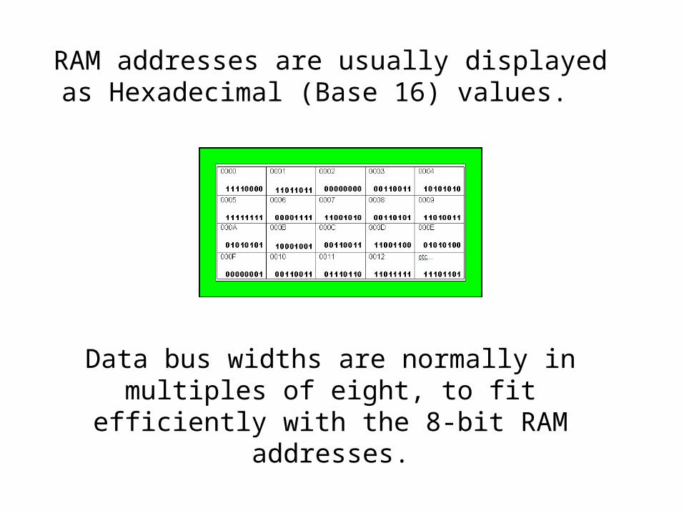
RAM addresses are usually displayed as Hexadecimal (Base 16) values.
Data bus widths are normally in multiples of eight, to fit efficiently with the 8-bit
RAM addresses.

The number of the correct address to be accessed is determined by the Memory Address Register. It uses the address bus to “point” to the relevant address.
Like the data bus, the address bus is several lines wide.A one-line address bus can point to, or “reference”, two locations – 0 and 1.
A two-line bus can reference 4 locations, i.e. 22
addresses.
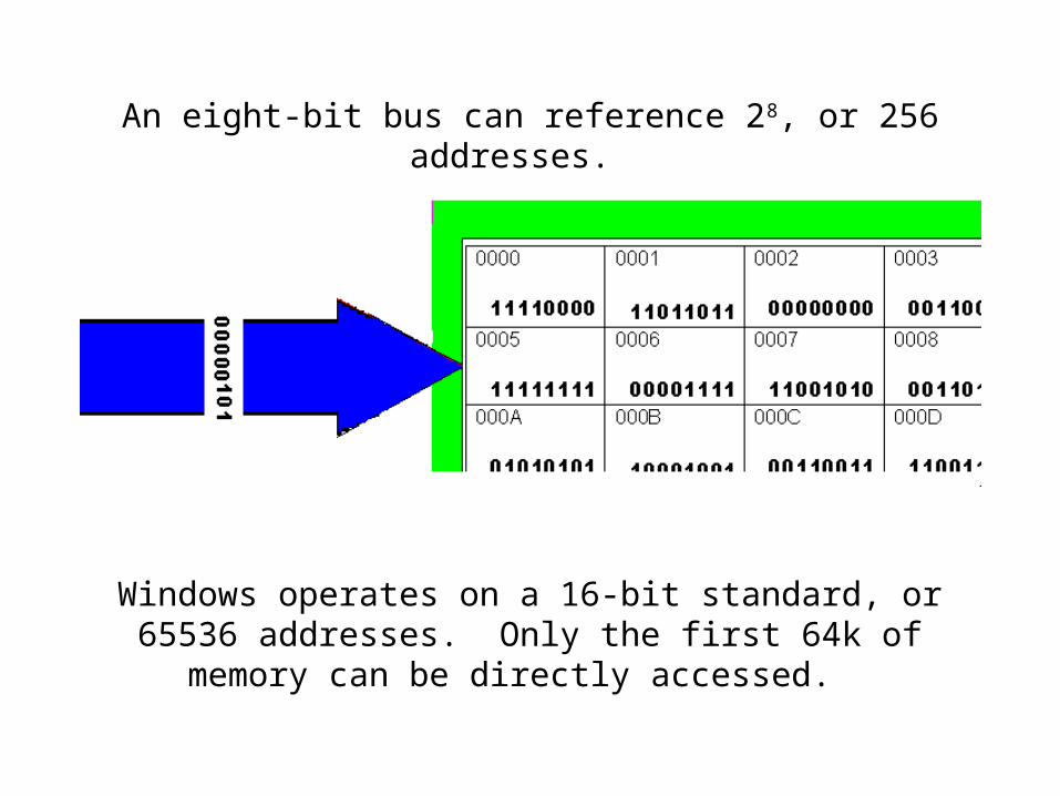
An eight-bit bus can reference 28, or 256 addresses.
Windows operates on a 16-bit standard, or 65536 addresses. Only the first 64k of memory can be
directly accessed.
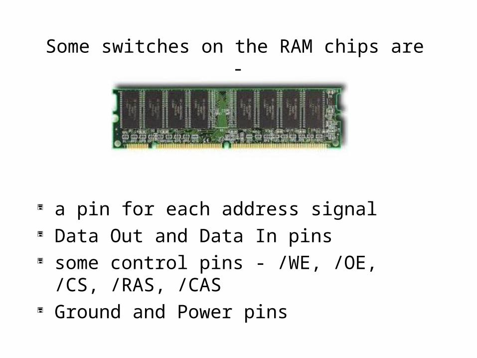
Some switches on the RAM chips are -
a pin for each address signal Data Out and Data In pins some control pins - /WE, /OE, /CS, /RAS,
/CAS Ground and Power pins
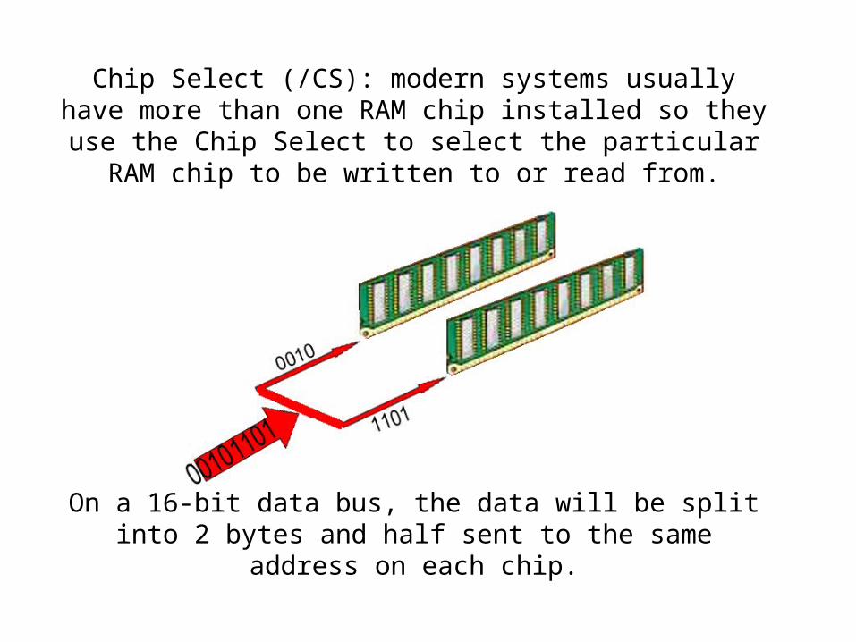
Chip Select (/CS): modern systems usually have more than one RAM chip installed so they use the Chip Select to select the particular RAM chip to be
written to or read from.
On a 16-bit data bus, the data will be split into 2 bytes and half sent to the same address on each
chip.

Write Enable (/WE) and Output Enable (/OE): these pins let the RAM know whether is is to be
read from or written to.

The Row Address Select switch (/RAS) is used to activate the proper row line.
Then the Column Address Select switch (/CAS) is used to activate the proper column. (In some modern RAM models the /CAS also acts as the /OE.)
The CPU then targets the cell where the two cross.

CHIP READ Place the address to be read on the address pins via
the address bus.
Activate Chip Select to select the RAM chip.
Activate the /OE pin so that the RAM knows
it's being read from.
The row address is placed on the address pins via the address
bus.

The /RAS pin is activated, which places the row address onto the Row Address Latch.
The /CAS pin is activated, which places the column address on the Column Address Latch.
The data in the cell being read is copied to the Data Out pin.
The data then gets moved onto the data bus to travel back to the MDR.
/RAS and /CAS are both deactivated so that the cycle can begin again.
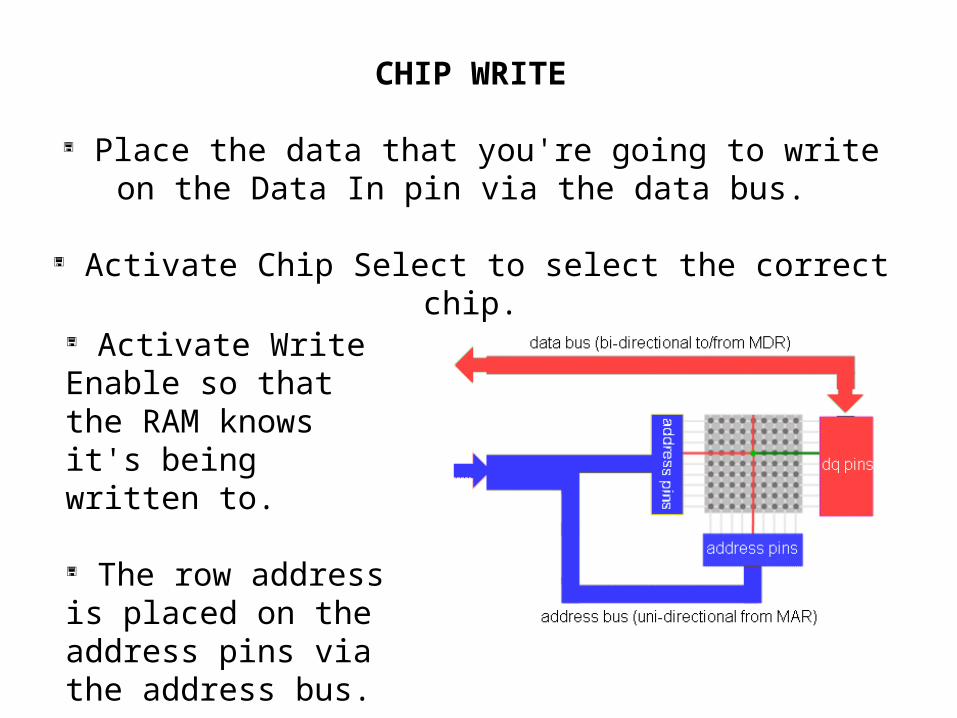
CHIP WRITE
Place the data that you're going to write on the Data In pin via the data bus.
Activate Chip Select to select the correct chip.
Activate Write Enable so that the RAM knows it's being written to.
The row address is placed on the address pins via the address bus.

The data placed on the Data In pin is written to the selected cell.
/RAS and /CAS are both deactivated so that the cycle can begin again.
The /RAS pin is activated, which places the row address onto the
Row Address Latch.
The /CAS pin is activated, which places the column address on the
Column Address Latch.

Summary
RAM locations are arranged as a grid, in rows and columns.
Each RAM chip has a Row Address Select (/RAS) and Column Address Select (/CAS) to locate the correct
address.
The Output Enable (/OE) and Write Enable (/WE) lets the chip know whether it is being read from or
written to.
Where more than one chip is installed, the Chip Select (/CS) accesses the correct one.
Data is transferred between the MDR and RAM along the data bus and through the DQ pins.