d 2.10 piezomems design platform, final version · piezomems design platform, final version due...
TRANSCRIPT
Page 1
Project no.: 229196
Project acronym:
piezoVolume
Project full title:
High volume piezoelectric thin film production process for microsystems
Collaborative Project targeted to a special group (such as SMEs)
Grant Agreement No.:
NMP2-SE-2009-229196
Start date of project: 2010-01-01 Duration: 3 years
D 2.10 PiezoMEMS design platform, final version
Due delivery date: 2010-12-31
Actual delivery date: YYYY-MM-DD
Organisation name of lead contractor for this deliverable: COV
Project co-funded by the European Commission within the Seventh Framework Programme (2008-2011)
Dissemination Level
PU Public X
PP Restricted to other programme participants (including the Commission Services)
RE Restricted to a group specified by the consortium (including the Commission Services)
CO Confidential , only for members of the consortium (including the Commission Services)

Page 2
Deliverable number: D 2.10
Deliverable name: PiezoMEMS design platform, final version
Work package: WP 2 – Tool developement
Lead contractor: COV
Author(s)
Name Organisation E-mail
Aurélie Cruau COV [email protected]
Gerold Schropfer COV [email protected]
Abstract
The following document presents design methodology improvements brought to Coventor tools suite to enable PiezoMEMS devices modelling and improve analyses. It first presents the Process Design Kits implementation in SEMulator3D, CoventorWare and MEMS+. Design Kits are made of Material Database, Process Descriptions specific to each tools and template layouts. Then a second part is dedicated to our latest tool behavioural modelling MEMS+ and the addition of a piezoelectric layer into flexible plates elements to take into account both actuation and sensing behaviour of PiezoMEMS devices. Last part is the description of the electrical circuit option added in the Finite Element mechanical solver MemMech of CoventorWare tool enabling a realistic analysis of piezoelectric sensing which has a direct impact on energy harvesters study.
Public introduction1
The following document presents design methodology improvements brought to Coventor tools suite to enable PiezoMEMS devices modelling and improve analyses. It first presents the Process Design Kits implementation in SEMulator3D, CoventorWare and MEMS+. Design Kits are made of Material Database, Process Descriptions specific to each tools and template layouts. Then a second part is dedicated to our latest tool behavioural modelling MEMS+ and the addition of a piezoelectric layer into flexible plates elements to take into account both actuation and sensing behaviour of PiezoMEMS devices. Last part is the description of the electrical circuit option added in the Finite Element mechanical solver MemMech of CoventorWare tool enabling a realistic analysis of piezoelectric sensing which has a direct impact on energy harvesters study.
1 According to Deliverables list in Annex I, all restricted (RE) deliverables will contain an introduction that will be
made public through the project WEBsite

Page 3
TABLE OF CONTENTS
Page
1 INTRODUCTION ................................................................................................................... 4
2 PDKS ....................................................................................................................................... 6 2.1 Material Databases ....................................................................................................... 6
2.1.1 Virtual Prototyping ........................................................................................... 6 2.1.2 Behavioral and Finite Element Modeling ......................................................... 6
2.2 Process Descriptions ..................................................................................................... 9 2.2.1 Virtual Prototyping ......................................................................................... 10
2.2.2 Behavioral Modeling and Finite Element Modeling ...................................... 10 2.3 Layout template .......................................................................................................... 11 2.4 Conclusion .................................................................................................................. 12
3 PARAMETRIC LIBRARY IMPROVEMENT: PIEZOELECTRIC SHELL ...................... 13 3.1 Shell element model ................................................................................................... 13 3.2 Adding the piezoelectric effect ................................................................................... 14
4 FEA SOLVER ADD-ON FOR PIEZOMEMS ..................................................................... 15
4.1 Description ................................................................................................................. 15 4.2 Extra Material ............................................................................................................. 16
5 CONCLUSION ..................................................................................................................... 17

Page 4
1 INTRODUCTION
Different tools for the design and modeling of piezoMEMS have been developed and are
available. These software tools are calibrated to the PZT processes and enable engineers to
simulate and optimize piezoMEMS designs before committing to build-and-test cycles.
Coventor’s MEMS+ and CoventorWare provide a design and simulation platform for MEMS
designers, enabling them to simulate end-product performance specs such as sensitivity,
linearity, frequency response, signal-to-noise, and temperature stability. SEMulator3D is a
unique modeling tool for virtual fabrication, enabling them to review designs and detect process
issues in advance of actual fabrication.
MEMS+ TM
A behavioral modelling tool which allows quickly exploring design alternatives and optimizing
performance at high accuracy. The platform is composed of 3 modules: a material database, a
process editor and Innovator which is the 3D builder of the MEMS structure.
The design platform MEMS+ allows to, quickly explore design alternatives, and to optimize
performance with high accuracy. With Coventor’s design flow the PZT technology comprising
material and process data is already defined. To start with, a model of the piezoelectric device is
constructed in MEMS+. Here, the MEMS designer works in a 3D graphical environment to
assemble a parametric model using high-order MEMS-specific finite elements (piezo-
mechanical shells). Each element is linked to the process description and material database so
that piezoelectric material properties and electrodes are assigned automatically. The high-order
elements give a precise mathematical description of the device physics using a low number of
degrees of freedom. This enables rapid, accurate simulation of the device physics in
Matlab/Simulink, and the ability to easily co-simulate the device with the conditioning circuit in
Cadence Virtuoso. For example, the designer can tune the piezoMEMS device dimensions to
attain a maximum actuation displacement or a certain resonance frequency before simulating the
device with different electronic circuits to compare the performance of each type.
COVENTORWARETM
A multi-physics field solver based analysis framework (Finite Element and Boundary Element
methods) including a materials property database, a process and layout editors, a 3-D model and
mesh generator, and field solvers for electrostatics and mechanics, the latter with boundary
conditions and features for PiezoMEMS. It includes a process entry user interface with a ready
to use library of foundry processes, e.g. MoveMEMS SINTEF process.
For PiezoMEMS device the module of interest is MEMMECH.
Further detailed modelling can be undertaken using CoventorWare’s field (or Finite-Element))
solvers to investigate details of the design. For example, the design can be checked for high
stress areas that may lead to breakage when the device is overloaded due to a shock. Gas
damping coefficients can also be simulated and included in the MEMS+ model to accurately
predict the Q-factor. An additional benefit is that simulation results from MEMS+ and
CoventorWare can be verified against each other. Simulating piezoelectric harmonic analysis
with a linear resistive load is one such example of a point of comparison between both tools.
Coventor’s solution for piezoelectric devices combines MEMS+ and CoventorWare to provide
hybrid solution that solves the coupled and multi-domain physics not addressed with traditional
point tools.

Page 5
SEMULATOR3DTM
A Virtual Prototyping tool which uses novel "voxel" technology (volumetric pixels) to build
highly detailed, virtual prototypes. Input is from 2D masks in industry-standard GDSII format,
along with a description of the specific fabrication process.
SEMulator3D offers a productive methodology that enables engineers to understand and
communicate process flow and device design through interactive visualization and quantitative
measurements. Areas of usage include process documentation, process modeling and
optimization, process communications with foundry customers and piezoMEMS design
verification prior to actual fabrication.
This report explains all new features and improvements done for enabling and easing
piezoMEMS design. They are presented in three parts. The first one describes the
implementation of Process Design Kits in each tool. The second one gives an overview of the
new Piezoelectric Flexible Plate model added to our existing library of behavioural components
included in MEMS+ and its advantages. The third one presents the options added to the standard
FEA solver Analyzer to broaden the scope of piezoMEMS devices which can be studied by the
solver.

Page 6
2 PDKS
The three tools MEMS+ (Behavioural Modelling), CoventorWare (Finite Element Modelling),
and SEMulator3D (Virtual Prototyping) need technology inputs. A technology is basically
described by the materials properties (like PZT or Silicon) and the fabrication process (stack of
deposition and etch of layers). Depending on the tool, you’ll need different data and level of
accuracy in the description. The first paragraph starts describing what has been done to update
the SINTEF MoveMEMS Material Database. Then the second paragraph is a summary of
implementation of MoveMEMS process in all tools.
2.1 Material Databases
2.1.1 Virtual Prototyping
SEMulator3D is a fabrication emulating tool. It requires only material names, type (conductor or
dielectric) and colours. Figure 2.1 shows the MoveMEMS SEMulator3D material database
(.vmpd file content) which is attached to the process description file. This can be checked in the
file properties.
Figure 2.1 SEMulator3D Material Database
2.1.2 Behavioral and Finite Element Modeling
MEMS+ and CoventorWare require the physical materials properties (electrical, mechanical,
thermal and piezoelectric) to simulate piezoMEMS devices operation. The following values in
table 2.1 have been integrated into both tools.
Note: TiO2 has not been used because it is a very thin oxide (100nm) under PZT only used for process A. It can be
neglected for simulations. Yet if it is required its properties are to be provided by SINTEF.

Page 7
Pro
pe
rtie
sS
ILIC
ON
_1
00
OX
IDE
TH
ER
M_
OX
IDE
PZ
TA
u-C
r A
u-T
iW
me
tal3
or
top
ele
ctr
od
eP
t-T
iB
CB
pas
siv
ati
on
laye
r
cu
bic
:C
xxxx=
Cyy
yy=
13
2G
Pa
Ex=
Ey=
Ez=
13
0.1
8 G
Pa
Cxx
yy=
71
GP
a
Gxy=
Gxz
=G
yz=
79
.6 G
Pa
Cxx
zz=
Cyy
zz=
73
GP
a
wa
fer
10
0 o
rie
nte
dC
zzzz=
11
5G
Pa
Cyz
yz=
Czxz
x=2
6G
Pa
Po
iss
on
ra
tio
nxy=n
xz=n
yz=
0.2
78
0.3
0.3
Cxy
xy=
30
GP
a0
.35
0.3
50
.35
0.3
4
De
ns
ity
23
31
kg
/m3
22
20
kg
/m3
22
20
kg
/m3
77
50
kg
/m3
19
30
0 k
g/m
31
93
00
kg
/m3
21
45
0 k
g/m
31
05
0
Re
sid
ua
l S
tre
ss
0-3
00
MP
a-3
00
MP
a1
75
MP
a2
82
MP
a2
82
MP
a7
00
MP
a-0
.1xT
+5
7.3
15
28
MP
a a
t 2
93
.15
K
Th
erm
al C
oe
f. o
f
Exp
an
sio
n1
.39
62
2e
-5 /K
1.3
96
22
e-5
/K
8.8
63
49
e-6
/K
4.1
94
e-5
/K
zero
str
es
s T
em
p.
=2
93
.15
K4
.5e
-9*T
+1
.27
33
e-5
4.5
e-9
*T +
1.2
73
3e
-52
.6e
-9*T
+8
.15
33
e-6
1.2
7e
-7*T
+4
.71
e-6
Th
erm
al
co
nd
uctivi
ty1
57
W/(
m*K
)1
.42
26
W/(
m*K
)1
.42
26
W/(
m*K
)1
.5 W
/(m
*K)
29
7 W
/(m
*K)
29
7 W
/(m
*K)
71
.6 W
/(m
*K)
7.3
81
e-4
*T+
7.4
18
e-2
0.2
94
W/(
m*K
) a
t 2
97
.15
K
Sp
ecific
he
at
70
3 J
/(kg
*K)
10
00
J/(
kg
*K)
10
00
J/(
kg
*K)
01
28
.7 J
/(kg
*K)
12
8.7
J/(
kg
*K)
13
3 J
/(kg
*K)
_
Ele
ctr
ica
l
co
nd
uctivi
ty1
40
0 S
/m1
e-1
0 S
/m1
e-1
0 S
/m2
.5e
-7 S
/m4
.4e
7 S
/m4
.4e
7 S
/m1
e7
S/m
1e
-17
S/m
Pe
rmittivi
ty0
3.9
3.9
erx=e
ry=e
rz=
16
00
00
02
.65
ex,
zx=
ey,
yz=
10
.5 C
/m2
ez,x
x=e
z,y
y=-4
.1 C
/m2
ez,z
z=
14
.1 C
/m2
2.9
Gp
a
_
Yo
un
g M
od
ulu
s7
0 G
Pa
78
GP
a1
68
GP
a
2.4
9e
-6 /K
5e
-7/K
2.5
e-6
/K
Pie
zoe
lectr
ic
co
effic
ien
ts_
__
_
70
GP
a
5e
-7/K
_
78
GP
a
_
Tab
le 2
.1:
Mat
eria
l d
atab
ase

Page 8
In Coventorware the technology is set in the model builder by browsing the corresponding files
in the Build Solid Model window. Materials (.mpd file), process (.proc) and layout inputs are
required to build the 3D meshed model necessary for mechanical and piezoelectric analyses. The
Material Database is shown in Figure 2.2.
Figure 2.2 CoventorWare MPD for SINTEF showing PZT properties

Page 9
MEMS+ tool allows more flexibility in the Material Database. It can include statistical data
(distribution, limits, ...) as can be seen in Figure 2.3. All material and process step properties
(such as Modulus of elasticity, layer thicknesses, side-wall angles etc.) can be defined as
absolute values, variables or algebraic equations. A combination of variables and algebraic
equations allows for properties to be mutually dependent on other properties, environmental
variables (e.g. temperature and humidity) or even entirely abstract variables such as the
equipment settings of a given fabrication process.
Figure 2.3: Material database for MoveMEMS in MEMS+
The MEMS+ design environment for PDK gives the foundry full control over which variables
are to be exposed (and so transferred and controlable) to the process editor.
2.2 Process Descriptions
Once materials set the next step is to define the clean room process using those materials to
create PiezoMEMS devices.

Page 10
2.2.1 Virtual Prototyping
The description for SEMulator3D should be detailed enough to obtain a highly realistic-looking
device or chip. More steps and more options are available to reach that aim. All steps of the GUI
(General User Interface) correspond to a python function and the complete process is scriptable
and can be run as a text file in a shell command. Figure 2.4 shows the process file created.
Figure 2.4 SEMulator3D SINTEF MoveMEMS process with C variant enabled.
2.2.2 Behavioral Modeling and Finite Element Modeling
CoventorWare process editor looks like SEMulator3D except only five basic operations (three
deposits and two etches) can be combined to create the 3D solid. The aim here is to obtain a
meshed model, consequently the device shape is optimized for simulation by simplifying the
geometry. An option for rounding corners is available to improve the final device. It is not used
in the SINTEF process but can be added by the user.
Figure 2.5 CoventorWare SINTEF MoveMEMS process

Page 11
MEMS+ process editor is used as in CoventorWare to give the 3rd
dimension (extrude direction
of process) to the device. It needs only the thickness and relative position of layers in the stack.
The same three basic deposit operations and two etch ones are available but it means only a z
initial position for layers middles and their thicknesses. The etch steps with masks names (names
given from MoveMEMS DRM) are also implemented directly after the deposit of the layer so
the order is slightly different than what has been done for CoventorWare.
Figure 2.6 MEMS+ SINTEF MoveMEMS process
The GDS numbers of layout layers will also be added in future MEMS+3 release. These
numbers are subject to change and users should ask SINTEF for an update on the technology
before using the PDK.
2.3 Layout template
For SEMulator3D, layout templates (one for process B and C and one for process A as SINTEF
used during the project) are necessary to translate GDS file into .cat format. This is to link the
GDS numbers to layer names.
Some devices are also included like the ones of Figure 2.7.
Figure 2.7 Cantilever and piston mirror device layout (see D5.6).
Page 12
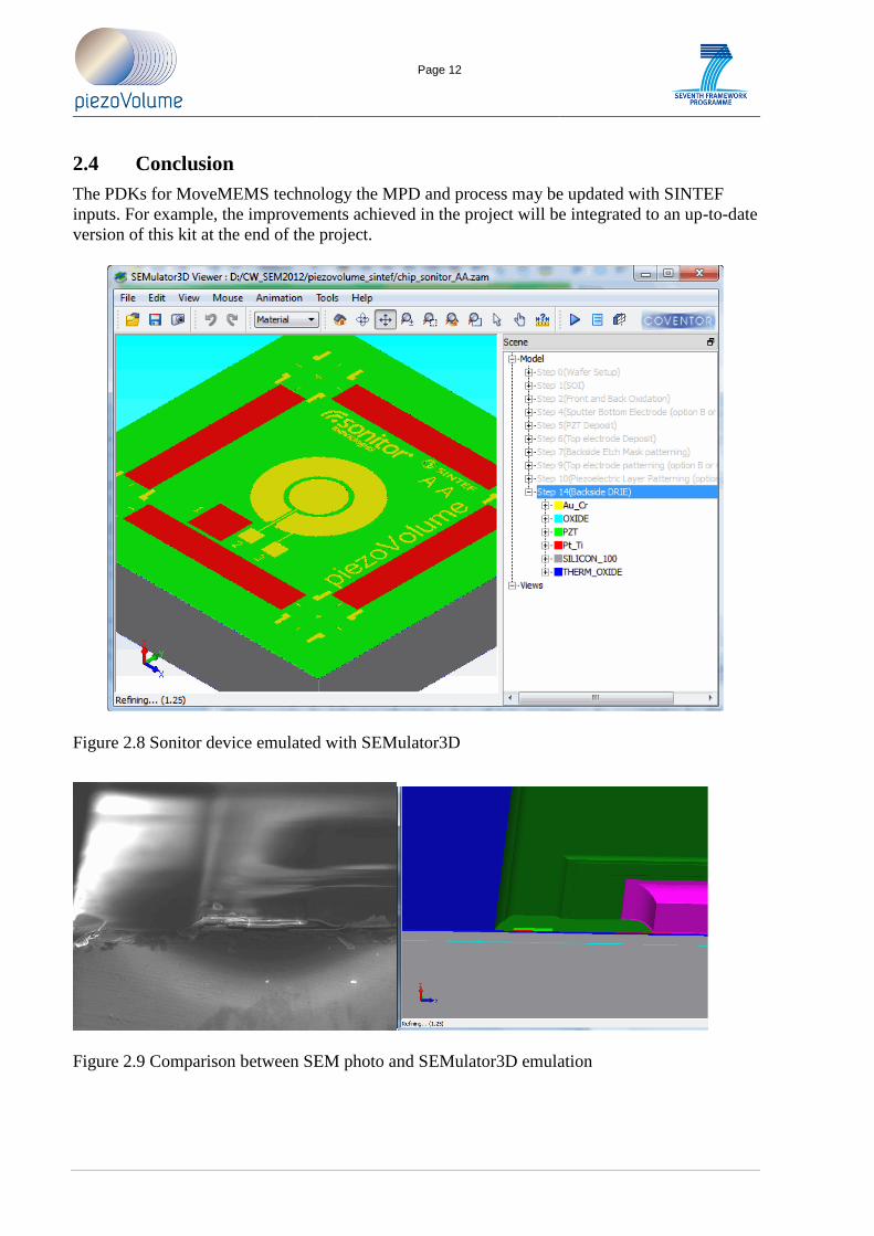
2.4 Conclusion
The PDKs for MoveMEMS technology the MPD and process may be updated with SINTEF
inputs. For example, the improvements achieved in the project will be integrated to an up-to-date
version of this kit at the end of the project.
Figure 2.8 Sonitor device emulated with SEMulator3D
Figure 2.9 Comparison between SEM photo and SEMulator3D emulation

Page 13
3 PARAMETRIC LIBRARY IMPROVEMENT: PIEZOELECTRIC
SHELL
3.1 Shell element model
This component is part of MEMS+ library. It can be combined with other components to build a
MEMS structure as in Figure 3.1.
Figure 3.1 MEMS+ device modeling example
The individual material layers of the plates are modeled by a state-of-the-art, nonlinear finite
element based on the mixed interpolation of tensorial components approach (MITC). The core
functionality of the underlying code is derived from a finite shell element (MITCn) written by
Dominique Chapelle and Marina Vidrascu at INRIA ("Institut National de Recherche en
Informatique et en Automatique, France"). Refer to The Finite Element Analysis of Shells:
Fundamentals, Springer, 2003, D. Chapelle, and K. J. Bathe. For an in-depth and detailed
explanation of the underlying mathematical model of the used MITCn element. A few
fundamental assumptions are summarized below:
The stress through the thickness of the plate/shell is zero.
The MITC elements are based on the theory of plates with transverse shear deformations.
This theory, developed by E. Reissner and R. D. Mindlin, uses the assumption that
particles of the plate originally on the straight line that is normal to the undeformed
middle surface remain on the a straight line during deformation, but this line is not
necessarily normal to the deformed middle surface. The flexible plate elements are
capable of handling shear stress.

Page 14
The plates have two parameters for specifying order of the polynomial, and the
underlying isoparametric finite element formulation expresses element coordinates and
element displacements in the form of interpolations using the natural coordinate system
of the element. The higher-order elements shows a significantly more accurate bending
behavior, which comes at the price of larger simulation time resulting from the
additional degrees of freedom (DOFs) used for the Interpolation.
3.2 Adding the piezoelectric effect
To add a piezoelectric layer you need first to use in the stack a material from the Material
Database which has a piezoelectric coefficient matrix e. Then on a flexible plate (rectangular or
other shapes) you right click to add a Piezoelectric Layer. Once added, top and bottom
electrodes appear as Electrical connectors named E1 and E2 by default (if no other electrical
connectors have been added prior to that step).
Figure 3.2 How to add a piezolayer in MEMS+ flexible plates.
During the simulation, a voltage-dependent piezoelectric stress σp is applied to the PZE layer:
σp = –eE, where E is the electric field vector in the PZE layer : E=Ez=(Vbottom-Vtop)/ h
h is the thickness of the piezoelectric layer, and (Vbottom-Vtop) is the voltage difference applied
between the two electrical pins E1 and E2.
The built-in PZE layer model can also be used for piezoelectric sensing. Piezoelectric sensing is
modeled by creating a stress/strain-dependent current flow between the element pins. The total
current i, including the electrical current generated by the internal resistance 1/ ρ, the
capacitance cap and the PZE layer strain depending charge Q is calculated as follows:

Page 15
4 FEA SOLVER ADD-ON FOR PIEZOMEMS
4.1 Description
PiezoMEMS devices typically exist within a larger electrical circuit. In some cases, the
mechanical simulation of the MEMS device requires modeling all or part of this larger circuit.
The new option enables harmonic analyses of piezoMEMS device including simple circuit
elements, such as resistors, inductors, and capacitors.
Two typical applications for this circuit element capability are
Energy harvesters, where vibration produces electrical current to other components in the
circuit.
Active damping, where patches of piezoelectric material are added to a larger mechanical
structure to control its vibration. As the structure vibrates, current is produced by the
piezoelectric material and directed to a resistor in the circuit. The resistor converts part of
this current to heat, thus dissipating the motion.
In CoventorWare tool you need to use MemMECH module for new analysis and set the
Piezoelectric physics and the Direct Harmonic Additional Analysis, then Circuit Elements
boundary conditions appears in the menu. Three components are available to build a small
circuit: resistor, capacitor, or inductor. They are attached to two terminals, denoted Terminal_1
and Terminal_2, which are surfaces with potential, floating conductor or electrical_node
boundary conditions are defined.
An Electrical_Node is simply a new circuit node added to the model to which additional circuit
elements can be attached; this allows the creation of simple RLC circuits.
These Electrical_Nodes are implicit; they are not actual entities in the solid model.
When one or more resistors are included in the model, electrical current is converted to heat and
dissipated from the model. As mentioned above, this typically damps the motion of the structure.
Figure 4.1: New Circuit Element Boundary Conditions
The circuit element applications described above usually do not include active electrical
elements. However, it is possible to include an active AC voltage source in a MemMech analysis
by defining an extra block of piezoelectric material that is fixed to prevent motion and has a
fixed potential on one electrode and an harmonic potential on the counter electrode surrounding
the piezoelectric layer. The desired electrical potential is prescribed on the counter electrode.
This approach can be used to verify a circuit model before including it in the larger
electromechanical simulation.

Page 16
The main results obtained from this simulation are the amount of energy dissipated the amount
of damping resulting from this current dissipation (Quality Factors menu). Other results include
currents, power and node potentials.
Figure 4.2 Results Window and example graph
4.2 Extra Material
To support people using this new option we have added an application note to the explanation
given above. It is part of the document called CoventorWare Application Notes as section2:
“Modeling Circuit Elements for PZE Analysis”. This document is included in the installation
folder. This note examine a simplified energy scavenger analyzed in "A Distributed Parameter
Electromechanical Model for Cantilevered Piezoelectric Energy Harvesters," Erturk, A. and D.
J. Inman, Journal of Vibration and Acoustics, 130, 4, August 2008. Results from MemMech are
compared with the analytical results, and it is shown that all both methods predict similar
mechanical and electrical behavior for this device.
Deliverable 5.6 will contain more application notes on using our tools for piezoMEMS devices.
Figure 4.3 Application Note Energy harvester device

Page 17
5 CONCLUSION
All improvements presented in paragraphs 3 and 4 have been integrated into tools which have
been released this CoventorWare and MEMS+. The PDKs are available on request and will be
integrated in the software. They may be updated with SINTEF’s input and agreement. The
deliverable 5.6 will present the PiezoMEMS devices studied with Coventor tools.