cyclic boolean circuits - paradise · cyclic boolean circuits marc d. riedel electrical and...
TRANSCRIPT

Cyclic Boolean CircuitsI
Marc D. Riedel
Electrical and Computer Engineering, University of Minnesota, Minneapolis, MN 55455
Jehoshua Bruck
Electrical Engineering, California Institute of Technology, Pasadena, CA 91125
Abstract
A Boolean circuit is a collection of gates and wires that performs a mapping from
Boolean inputs to Boolean outputs. The accepted wisdom is that such circuits must
have acyclic (i.e., loop-free or feed-forward) topologies. In fact, the model is often de-
fined this way – as a directed acyclic graph (DAG). And yet simple examples suggest
that this is incorrect. We advocate that Boolean circuits should have cyclic topologies
(i.e., loops or feedback paths). In other work, we demonstrated the practical implica-
tions of this view: digital circuits can be designed with fewer gates if they contain cy-
cles. In this paper, we explore the theoretical underpinnings of the idea. We show that
the complexity of implementing Boolean functions can be lower with cyclic topologies
than with acyclic topologies. With examples, we show that certain Boolean functions
can be implemented by cyclic circuits with as little as one-half the number gates that
are required by equivalent acyclic circuits.
Keywords: Boolean circuits, Boolean functions, combinational circuits, cyclic
circuits, DAG, cycles, loops, feedback
IThis work is partially supported by an NSF CAREER Award (grant CCF0845650), by the NSF Expe-ditions in Computing Program (grant CCF-0832824), by a grant from the MARCO Focus Center ResearchProgram on Functional Engineered Nano-Architectonics (FENA), and by the Caltech Lee Center for Ad-vanced Networking.
Email addresses: [email protected] (Marc D. Riedel), [email protected] (JehoshuaBruck)
Preprint submitted to Discrete Mathematics December 3, 2009

1. Introduction
This paper presents circuit constructs that are counter-intuitive and run against the
accepted practice. Accordingly, throughout the paper, we adopt a discursive tone and
elucidate the ideas with many examples.
1.1. Boolean Circuit Model
The Boolean circuit model is a fundamental one in complexity theory. It is also the
core model underpinning practical digital circuit design. In general terms, a Boolean
circuit consists of gates and wires. Each gate corresponds to a Boolean function that
performs a mapping from several input bits to an output bit. The gates are connected by
wires, with the outputs of some being the inputs of others. Accordingly, the topology
of the circuit may be described as a directed graph G = (V, E), with the nodes V
representing logic gates and the edges E representing wires.
Central to the definition of the Boolean circuit model is the idea that such circuits
perform mappings from designated inputs to designated outputs. So each output of a
Boolean circuit computes a specific Boolean function:
f : {0, 1}n → {0, 1}. (1)
Of course, a collection of gates and wires can produce outputs that are not Boolean
functions. Such circuits can exhibit memory. We will use the term “Boolean circuit”
to refer to a circuit that produces outputs that depend only on the current inputs; dig-
ital circuit designers call these combinational circuits. We will use the term “not a
Boolean circuit” to refer to a circuit that produces outputs that depend not only on
the current inputs, but also on the previous inputs; digital circuit designers call these
sequential circuits.
The common way to categorize circuits is that Boolean circuits have acyclic topolo-
gies, while circuits with cyclic topologies have non-Boolean behavior. This conforms
to intuition. In an acyclic circuit, such as that shown in Figure 1, the input values prop-
agate forward and determine the values of the outputs. The outcome can be asserted
regardless of the prior values on the wires and so independently of the past sequence
of inputs. The circuit is clearly Boolean (it implements the exclusive-or of x and y.)
2

In a cyclic circuit, such as that shown in Figure 2, the behavior is more intricate.
A common approach is to characterize the output values and the next state in terms of
the input values and the current state. The current state, in turn, depends on the prior
sequence of inputs (starting from some known initial state). The circuit in Figure 2 is
not a Boolean circuit: given input values s = 0 and r = 0, we cannot determine the
output without knowing the value of z3 or z4. (In fact, the circuit implements a one-bit
memory element, called a latch.)
�
�
�
�
���
��
���
�
��
��
Figure 1: An acyclic circuit
�
�
�
���
���
��
��
Figure 2: A cyclic circuit.
Clearly:
• An acyclic topology is sufficient for a circuit to be Boolean.
• Conversely, a cyclic topology is necessary for a circuit not to be Boolean.
But we ask:
• Is an acyclic topology necessary for a circuit to be Boolean?
The accepted wisdom is that, yes, Boolean circuits must have acyclic topologies. In
fact, Boolean circuits are often defined as directed acyclic graphs (DAGs): e.g., (Pa-
padimitriou, 1995, p. 80) and (Vollmer, 1999, p. 8). Circuit practitioners design com-
binational circuits without cycles: e.g., (Katz, 1992, p. 14) and (Wakerly, 2000, p.
193). Design automation tools enforce this constraint (Sentovich et al., 1992).
3

1.2. Cyclic Boolean Circuits
The accepted wisdom and theoretical practice are wrong: a circuit with a cyclic
topology can be Boolean. A trivial circuit, shown in Figure 3, demonstrates this. It
consists of an AND gate and an OR gate connected in a cycle, both with input x.
Recall that the output of an AND gate is 0 iff either input is 0; the output of an OR gate
is 1 iff either input is 1. Consider the two possible values of x.
• On the one hand, if x = 0, the output of the AND gate is fixed at 0, and so the
input from the OR gate has no influence, as shown in Figure 4 (a).
• On the other hand, if x = 1, the output of the OR gate is fixed at 1, and so the
input from the AND gate has no influence, as shown in Figure 4 (b).
Although useless, this circuit qualifies as Boolean: the value of the output f is com-
pletely determined by the current input value x (actually f = x).
� �
���� ��
Figure 3: A (useless) cyclic Boolean circuit.
0 0
00AND OR
1 1
11AND OR
(a) (b)
Figure 4: The circuit of Figure 3 with (a) x = 0 and (b) x = 1.
One might argue that, while Boolean circuits can be cyclic, such examples are
contrived or inconsequential. A convincing example suggesting otherwise is shown in
4
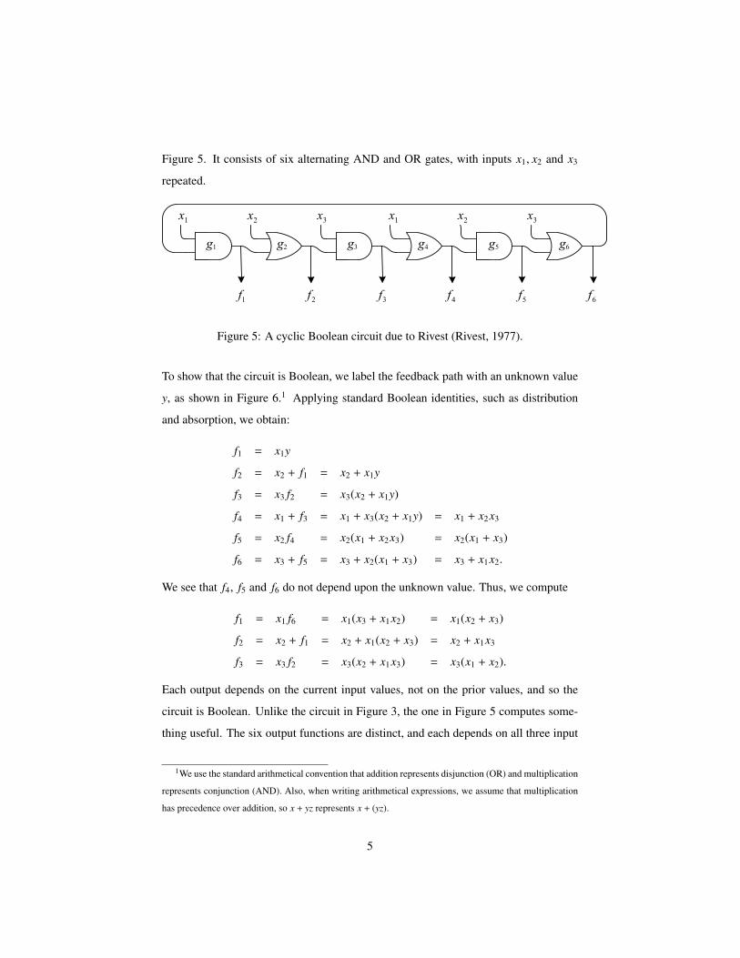
Figure 5. It consists of six alternating AND and OR gates, with inputs x1, x2 and x3
repeated.
1x
2x
3x
1x
2x
3x
1f
2f
3f
4f
5f
6f
g2g1 g3 g5g4 g6
Figure 5: A cyclic Boolean circuit due to Rivest (Rivest, 1977).
To show that the circuit is Boolean, we label the feedback path with an unknown value
y, as shown in Figure 6.1 Applying standard Boolean identities, such as distribution
and absorption, we obtain:
f1 = x1y
f2 = x2 + f1 = x2 + x1y
f3 = x3 f2 = x3(x2 + x1y)
f4 = x1 + f3 = x1 + x3(x2 + x1y) = x1 + x2x3
f5 = x2 f4 = x2(x1 + x2x3) = x2(x1 + x3)
f6 = x3 + f5 = x3 + x2(x1 + x3) = x3 + x1x2.
We see that f4, f5 and f6 do not depend upon the unknown value. Thus, we compute
f1 = x1 f6 = x1(x3 + x1x2) = x1(x2 + x3)
f2 = x2 + f1 = x2 + x1(x2 + x3) = x2 + x1x3
f3 = x3 f2 = x3(x2 + x1x3) = x3(x1 + x2).
Each output depends on the current input values, not on the prior values, and so the
circuit is Boolean. Unlike the circuit in Figure 3, the one in Figure 5 computes some-
thing useful. The six output functions are distinct, and each depends on all three input
1We use the standard arithmetical convention that addition represents disjunction (OR) and multiplication
represents conjunction (AND). Also, when writing arithmetical expressions, we assume that multiplication
has precedence over addition, so x + yz represents x + (yz).
5

1x
2x
3x
1x
2x
3x
1f
2f
3f
4f
5f
6f
g2g1 g3 g5g4 g6y
Figure 6: Analyzing the circuit of Figure 5.
variables. Moreover, we can show that this cyclic circuit has fewer gates than any
equivalent acyclic circuit. To see this, note that any acyclic configuration contains at
least one gate producing an output function that does not depend on the output of any
other gate producing an output function. (If this were not the case, then every output
gate would depend upon another and so the circuit would be cyclic.)
x2
x3
x1
)( 321 xxx +ANDOR
Figure 7: With fan-in two gates, two gates are needed to compute x1(x2 + x3).
With fan-in two gates, it takes two gates to compute any one of the six functions by
itself. This is illustrated in Figure 7. We conclude that an acyclic implementation of
the six functions requires seven gates, compared to the six in the cyclic circuit.
The circuit in Figure 5 was presented by Rivest in 1977, in a paper less than a page
long (Rivest, 1977). His work on the topic, as well as that of a few others in the 1960s,
seems to have gone largely unnoticed by theoreticians and practitioners alike. And yet
his example hints at a fundamental misconception in the field, namely that “Boolean
circuit” and “acyclic” are synonymous terms. In this paper, we demonstrate not only
that it is feasible to design Boolean circuits with cyclic topologies, but it is generally
advantageous to do so.
6

Given an upper bound on the time that it takes each gate to compute a value, the
delay of a circuit is an upper bound on the time that it takes for the circuit to compute
the values of the output functions. The delay is generally determined by the length of
the longest path from an input to an output, called the critical path. In any circuit –
cyclic or acyclic – there may exist false paths, that is to say, topological paths that are
never sensitized. If the longest path is false, it does not impinge upon the delay. The
critical path of the circuit then is the longest true path.
For a cyclic circuit, we can say that it is Boolean if all cycles are false; the sensitized
paths in the circuit never bite their own tail to form true cycles. The delay of a cyclic
circuit is not necessarily greater that than that of an acyclic circuit. It is simply the
length of the longest true path.
1.3. Prior and Related Work
In 1963, McCaw presented a thesis for his Engineer’s Degree at Stanford titled
“Loops in Directed Combinational Switching Networks” (McCaw, 1963). He demon-
strated the cyclic circuit shown in Figure 8 consisting of two AND gates and two OR
gates, with five inputs and two outputs. His analysis of the circuit was in the same
vein as that given in the previous section. He concluded that the circuit is Boolean and
computes the functions:
f1 = a + b + x(c + d + x f1) = a + b + x(c + d)
f2 = c + d + x(a + b + x f2) = c + d + x(a + b).
As with circuit in Figure 5, McCaw argues that his circuit has fewer AND and OR
gates than is possible with an acyclic circuit implementing the same functions.
Even earlier, in 1960, Short applied an abstract graphical model to the study of
switching networks with directional switches (Short, 1961). He argued that networks
must be cyclic for some minimal forms. In 1970, Kautz, Short’s Ph.D. advisor at Stan-
ford, presented a short paper on the topic of feedback in circuits with logic gates (Kautz,
1970). He described a cyclic circuit consisting of 6 fan-in two NOR gates with three
inputs and three outputs. Although plausible, his circuit is not Boolean according to
the rigorous model that we propose. (It assumes that all wires have definite Boolean
values at the outset.)
7

x
2f
1f
ba x dc
ORORAND AND
Figure 8: A cyclic Boolean circuit due to McCaw.
In 1971, Huffman discussed feedback in linear threshold networks. He claimed
that an arbitrarily large number of input variables can be complemented in a network
containing a single NOT element, provided that feedback is used (Huffman, 1971).
This improved upon an earlier result by Markov, demonstrating that k NOT elements
suffice to generate the complements of 2k−1 variables (Markov, 1958). As with Kautz’s
example, Huffman’s doesn’t quite work. Still, in an insightful commentary on his and
Kautz’s work, he hinted at the possible implications,
“ At this time, these [cyclic] examples are isolated ones. They do, however,
provide tantalizing glimpses into an imaginable area of future research.”
In 1977, Rivest presented a general version of the circuit in Figure 5 and proved
that it is optimal (Rivest, 1977). For any odd integer n greater than 1, the general circuit
consists of n fan-in two AND gates alternating with n fan-in two OR gates, with input
variables x1, . . . , xn arranged as in Figure 5. It produces 2n distinct output functions,
each of which depends on all n input variables. He proved that any acyclic circuit
implementing the same 2n output functions requires at least 3n − 2 fan-in two gates.
Thus, asymptotically, his cyclic implementation is at most two-thirds the size of the
best possible acyclic implementation.
In 1978, Khrapchenko was the first to recognize that depth and delay in a circuit are
not equivalent concepts (Khrapchenko, 1978). With false paths, the delay of a circuit
can be less than that of the longest path.
8

In more recent work, we advocated the design of cyclic circuits in practice. We dis-
cussed techniques for validating cyclic circuits (Riedel and Bruck, 2003a, 2004; Backes
et al., 2008). We proposed strategies for synthesizing cyclic circuits with computer-
aided design tools (Riedel and Bruck, 2003b; Backes and Riedel, 2009). Our syn-
thesis tool, CYCLIFY, optimizes the designs of circuits by introducing cycles in the
restructuring and minimization phases of logic synthesis. It reduces the number of
gates needed by overlapping the computation of multiple functions (as Rivest’s exam-
ple hinted at). It reduces the delay of circuits by moving computation off of critical
paths (as Khrapchenko’s work hinted at).
1.4. Overview
In this paper, we study cyclic Boolean circuits from a theoretical perspective: we
exhibit families of cyclic circuits that are optimal in the number of gates and we prove
lower bounds on the size of equivalent acyclic circuits. First, we present a cyclic cir-
cuit with only two gates and argue that an equivalent acyclic circuit requires three
gates. Next, we present a cyclic circuit with three gates and argue that an equivalent
acyclic circuit requires five gates. Finally, we present a family of cyclic circuits with n
gates and prove that an equivalent family of acyclic circuits requires at least 2n gates.
Accordingly, we conclude that the cyclic complexity of functions can be as little as
one-half of the acyclic complexity. Our lower bound is based on a fan-in argument: in
order to compute a function that depends on a certain number of variables using gates
with a certain fan-in, we require a tree of at least a certain size. We show that this is
largest gap that can be obtained with this fan-in lower bound technique.
9

2. Framework
2.1. Notation
Algebraically, we use the standard notation: addition (+) denotes disjunction (OR),
multiplication (·), denotes conjunction (AND), and an overbar (x) denotes negation
(NOT). The restriction operation (also known as the cofactor) of a function f with
respect to a variable x refers to the assignment of a constant value to x in the expression
for f . We use the notation f |x to denote the restriction of x to 1 and f |x to denote the
restriction of x to 0. A function f depends upon a variable x iff f |x is not identically
equal to f |x. Call the variables that a function depends upon its support set.
We will often represent functions in so called Reed-Muller form, a canonical form
consisting of exclusive-of (XOR) and conjunction (AND) operations. We denote XOR
with the symbol ⊕. As early as 1929, Zhegalkin showed that this representation is
canonical (Zhegalkin, 1929): if we multiply out all parentheses, perform the simplifi-
cations x ⊕ x = 0 and x · x = x, and sort the product terms, the resulting expression is
unique. For instance, the function
f = x1(x2 + x3).
is represented as
f = 1 ⊕ x1 ⊕ x2x3 ⊕ x1x2x3.
Note that 1 ⊕ x = x. When writing arithmetical expressions, we assume that AND has
precedence over XOR, so x ⊕ yz represents x ⊕ (yz). The Reed-Muller representation
has distinct advantages when manipulating expressions algebraically. In particular,
the dependence of a function on its variables is explicit: if a variable appears in the
expression, then the function depends on it.
2.2. Circuit Model
Graphically, a circuit consists of gates connected by wires. Each gate has one or
more inputs and a single output. The symbols for common gates are shown in Figure 9.
A bubble is used to indicate that an input or output is negated, as illustrated in Figure 10.
10

AND OR XOR NOT
Figure 9: Symbols for different types of gates.
�
�
�
Figure 10: Bubbles on the inputs or the output of a gate indicate negation.
Here z = x + y.
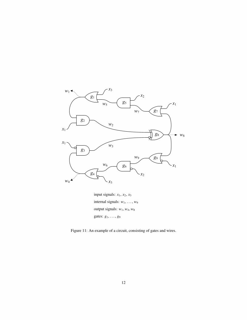
An example of a circuit is shown in Figure 11. Even though a wire may split in
our diagrams, as is the case with wire w8 in Figure 11, conceptually there is a single
instance of it. In general,
• A circuit accepts signals x1, . . . , xm, ranging over {0, 1}, called the primary in-
puts. Each primary input is fed into one or more gate inputs. Even though the
symbol for a primary input may appear in several places, as is the case with x1,
x2 and x3 in Figure 11, conceptually there is a single instance of it.
• The gates in the circuit produce internal signals, w1, . . . ,wn ranging over {0, 1,⊥}.
(We discuss the third value, ⊥, in Section 2.4.)
• A subset of the set of internal signals is designated as the set of primary outputs.
A gate implements a Boolean function, i.e., a mapping from Boolean inputs to a
Boolean output value,
g : {0, 1}d → {0, 1}.
The set of inputs to a gate are called its fan-in set. When we say a “fan-in d” gate, we
mean a gate with fan-in set of cardinality d. The set of gates that are attached to a gate
output are called its fan-out set.
11
x1
g8
w1
w3
w2
g5
x2
x3
g2
x1
x1
g9
g6
x2g4
x3
g3
x1
g7
g1
w4
w5
w6
w7
w9
w8
input signals: x1, x2, x3
internal signals: w1, . . . , w9
output signals: w1,w4,w8
gates: g1, . . . , g9
Figure 11: An example of a circuit, consisting of gates and wires.
12

2.3. Gate Model
Any discussion of circuit complexity is predicated on a restricted gate model of
some kind. Otherwise, with gates of arbitrary size and complexity, any function can
be implemented with a single “gate.” We restrict the scope of gates in two ways. The
first way is to bound the fan-in, as shown in Figure 12 (a). Each gate can have at most
d inputs, for some integer d ≥ 1. The second way is to restrict the type of gate. For
instance, we can limit ourselves to so-called “AND-OR-NOT” (AON) gates, i.e., AND
gates with the inputs and output possibly negated. An example of such a gate is shown
in Figure 12 (b). The general form of the Boolean function realized by an AON gate is
g(x1, x2, . . . , xd) = (x1 ⊕ c1) · (x2 ⊕ c2) · · · (xd ⊕ cd) ⊕ cd+1,
where c1, . . . , cd+1 are arbitrary choices of 0 and 1.
x1 x2 xd
x1 x2 x3
(a) (b)
Figure 12: Restricting the scope of gates. (a) Bound the fan-in. (b) Use AND gates
(with the inputs and output possibly negated).
2.4. Boolean Circuits
Analysis of an acyclic circuit is transparent. We first evaluate the gates connected
only to primary inputs, and then gates connected to these and primary inputs, and so
on, until we have evaluated all gates. The previous values of the internal signals do not
enter into play.
In a cyclic circuit, there are one or more strongly connected components. Recall
that in a directed graph G, a strongly connected component is an induced subgraph
S ⊆ G such that
13

• there exists a directed path between every pair of nodes in S ;
• for every node s in S and every node n outside of S , if there exists a path from s
to n (from n to s) then there is no path from n to s (from s to n, respectively).
We can analyze each strongly connected component separately.
We adopt a ternary framework for analysis. We assume that, at the outset, all
wires in a circuit have unknown or possibly undefined values, which we denote with
the symbol ⊥. We apply definite values to the inputs, and track the propagation of
signal values.
With only the primary inputs fixed at definite values, each gate in a strongly con-
nected component has some unknown/undefined inputs, valued ⊥. Nevertheless, for
each such gate we can ask: is there sufficient information to conclude that the gate
output is 0 or 1, in spite of the ⊥ values? If yes, we assign this value as the output;
otherwise, the value ⊥ persists. For instance, with an AND gate, if the inputs include a
0, then the output is 0, regardless of other ⊥ inputs. If the inputs consist of 1 and ⊥ val-
ues, then the output is ⊥. Only if all the inputs are 1 is the output 1. This is illustrated
in Figure 13. Input values that determine the gate output are called controlling.
0
⊥0
AND
1
⊥⊥
AND
1
1
1AND
Figure 13: An AND gate with 0, 1, and ⊥ inputs.
Consider the circuit fragment in Figure 14. One might be tempted to reason as
follows: the output of the AND gate g1 is fed in complemented and uncomplemented
form into the OR gate g2. Thus, one of the inputs to the OR gate must be 1, and so its
output must be 1. And yet, by definition, ⊥ designates an unknown, possibly undefined
value. (For instance, in an actual circuit, it could indicate a voltage value exactly half
way between logical 0 and logical 1.) In our analysis, we remain agnostic: the output
of the OR gate is ⊥.
In the analysis, we track the propagation of well-defined signal values. Once a
14

1
⊥ ⊥⊥
OR
g2
AND
g1
⊥
⊥
Figure 14: An illustration unknown/undefined values ⊥.
definite value is assigned to an internal wire, this value persists for the duration (so
long as the input values are held constant). For any input assignment, a circuit reaches
a so-called fixed point in the ternary framework: a state where no further updates
of controlling values are possible. This fixed point is unique (Brzozowski and Seger,
1995). We adopt the following definition.
A circuit is Boolean iff, for every assignment of input values, with all
the wires initially set to ⊥, the circuit reaches a fixed point that does not
contain any ⊥ values on the outputs.
We illustrate the analysis with two cyclic examples: one that is not Boolean and one
that is.
Example 1
Consider the circuit shown in Figure 15, consisting of an AND gate g1, an OR gate g2,
and an AND gate g3, in a cycle. By inspection, note that if x1 = 0 then f1 assumes
value 0; if x2 = 1 then f2 assumes value 1; and if x3 = 0 then f3 assumes value 0.
But what happens if x1 = 1, x2 = 0 and x3 = 1? In this case, all the outputs equal ⊥,
as illustrated in Figure 16. The outcome for all eight cases is shown in Figure 1. We
conclude that the circuit is not Boolean.
Example 2
Consider the circuit in Figure 17. Suppose that we apply inputs x1 = 1, x2 = 0, x3 = 1.
Gates g1, g3, g5 and g7 produce outputs of 1, 0, 0, and 1, respectively. Gate g2 produces
an output of 1. Gate g8 produces an output of 0. Gate g9 produces an output of 0. Gate
g6 produces an output of 0. Finally, gate g4 produces an output of 0. These values are
shown in Figure 17. The analysis for all eight input combinations is summarized in
Table 18. We conclude that the circuit is Boolean.
15

1x
2x
3x
1f
2f
3f
g2g1 g3
ORAND AND
Figure 15: A cyclic circuit that is not Boolean.
��
��
��
����� ���
� ��
⊥ ⊥ ⊥
Figure 16: The circuit of Figure 15 with x1 = 1, x2 = 0 and x3 = 1.
x1 x2 x3 f1 f2 f3
0 0 0 0 0 0
0 0 1 0 0 0
0 1 0 0 1 0
0 1 1 0 1 1
1 0 0 0 0 0
1 0 1 ⊥ ⊥ ⊥
1 1 0 0 1 0
1 1 1 1 1 1
Table 1: Analysis of the circuit in Figure 15.
16

g8
1
0
1
g5
g2
1
g9
g6
g4
g3
1
g7
g1
0
0
0
1
0
0
13x
02x
11x
11x
02x
13x
Figure 17: The circuit of Figure 11 with inputs x1 = 1, x2 = 0, x3 = 1.
x1 x2 x3 g1 g2 g3 g4 g5 g6 g7 g8 g9
0 0 0 0 0 1 1 0 1 0 0 1
0 0 1 1 0 1 1 0 1 0 0 1
0 1 0 0 0 1 1 0 0 0 0 1
0 1 1 1 0 0 0 1 0 1 1 1
1 0 0 0 0 0 1 0 1 1 1 1
1 0 1 1 1 0 0 0 0 1 0 0
1 1 0 1 1 0 1 1 0 1 0 0
1 1 1 1 1 0 0 1 0 1 0 0
Figure 18: Analysis summary for the circuit of Figure 11.
17
3. Optimality and Lower Bounds
Our general strategy in the following constructions is to present a cyclic circuit
that is optimal in the number of gates, and then prove a lower bound on the size of
any acyclic circuit implementing the same functions. (For what follows, when we say
circuit size, we mean the number of gates.) The argument for the optimality of the
cyclic circuit rests on two properties:
Property 1
Each of the output functions depends on all the variables.
Property 2
The output functions are pairwise distinct.
The cyclic circuit is shown to be optimal according to the following trivial claim (true
regardless of the gate model):
Claim 1
A circuit implementing m distinct functions consists of at least m gates.
Lower bounds on circuit size are notoriously difficult to establish. In fact, such
proofs are related to fundamental questions in computer science, such as the separa-
tion of the P and NP complexity classes. (To prove that P , NP it would suffice to
find a class of problems in NP that cannot be computed by a polynomially sized cir-
cuit.) Much of the recent work in circuit complexity has been spurred by these open
problems.
All existing lower bounds on circuit size are linear in the number of variables (Vollmer,
1999). In 1949, Shannon showed by a straight forward counting argument that nearly
all functions require circuits with an exponential number of gates (Shannon, 1949). Yet
there is no known explicit example (Wegener, 1987).
We prove that some cyclic Boolean circuits are smaller than equivalent acyclic
circuits based on a fan-in lower bound. We show that this is largest gap that we can
prove using the fan-in lower bound technique.
18

3.1. Fan-in Lower Bound
Our lower bound on the size of an acyclic circuit is formulated as a fan-in argument.
The essence of the argument was presented by Rivest (Rivest, 1977), although we
present it in a more general form.
A circuit can only compute a function of a given set of input variables if it “sees”
all of them. For example, in Figure 19, gate g2 can compute a function of x1, x2 and
x3; gate g1 cannot compute a function of x3 since it does not see x3. In an acyclic
��
��
��
��
��
��
Figure 19: A gate can only compute functions of variables that it “sees”.
circuit, there is a partial ordering among the gates: if a gate gi depends on a gate g j,
directly or indirectly, then g j cannot depend on gi, directly or indirectly. With a partial
ordering on the output functions, there must be at least one output function at the top
which depends upon no other. If this function depends on v input variables, the gate
producing it must be the root of a tree that sees all these v variables as leaves. The
lower bound is based on a calculation of the minimum number of gates in this tree.
Claim 2
An acyclic circuit implementing m distinct output functions, each depending on v input
variables, consisting of gates with fan-in at most d has at least⌈v − 1d − 1
⌉+ m − 1
gates. This is true for any fan-in value d ≥ 2.
19
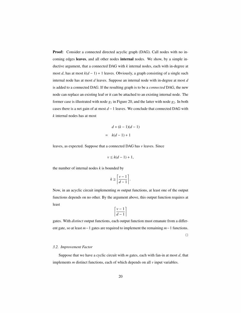
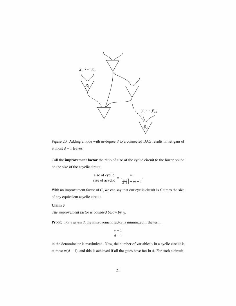
Proof: Consider a connected directed acyclic graph (DAG). Call nodes with no in-
coming edges leaves, and all other nodes internal nodes. We show, by a simple in-
ductive argument, that a connected DAG with k internal nodes, each with in-degree at
most d, has at most k(d − 1) + 1 leaves. Obviously, a graph consisting of a single such
internal node has at most d leaves. Suppose an internal node with in-degree at most d
is added to a connected DAG. If the resulting graph is to be a connected DAG, the new
node can replace an existing leaf or it can be attached to an existing internal node. The
former case is illustrated with node g1 in Figure 20, and the latter with node g2. In both
cases there is a net gain of at most d− 1 leaves. We conclude that connected DAG with
k internal nodes has at most
d + (k − 1)(d − 1)
= k(d − 1) + 1
leaves, as expected. Suppose that a connected DAG has v leaves. Since
v ≤ k(d − 1) + 1,
the number of internal nodes k is bounded by
k ≥⌈
v − 1d − 1
⌉.
Now, in an acyclic circuit implementing m output functions, at least one of the output
functions depends on no other. By the argument above, this output function requires at
least ⌈v − 1d − 1
⌉gates. With distinct output functions, each output function must emanate from a differ-
ent gate, so at least m−1 gates are required to implement the remaining m−1 functions.
2
3.2. Improvement Factor
Suppose that we have a cyclic circuit with m gates, each with fan-in at most d, that
implements m distinct functions, each of which depends on all v input variables.
20
��
��
����
��
��
��
Figure 20: Adding a node with in-degree d to a connected DAG results in net gain of
at most d − 1 leaves.
Call the improvement factor the ratio of size of the cyclic circuit to the lower bound
on the size of the acyclic circuit:
size of cyclicsize of acyclic
=m⌈
v−1d−1
⌉+ m − 1
.
With an improvement factor of C, we can say that our cyclic circuit is C times the size
of any equivalent acyclic circuit.
Claim 3
The improvement factor is bounded below by 12 .
Proof: For a given d, the improvement factor is minimized if the term
v − 1d − 1
in the denominator is maximized. Now, the number of variables v in a cyclic circuit is
at most m(d − 1), and this is achieved if all the gates have fan-in d. For such a circuit,
21
the improvement factor is
m⌈m − 1
d−1
⌉+ m − 1
=m
2m − 1≥
12
if d ≥ 3 andm
2m − 2≥
12
if d = 2. 2
3.3. Rivest’s Circuit
Consider the circuit shown in Figure 21, due to Rivest (Rivest, 1977). This is the same
circuit as in Figure 5, shown again for the reader’s convenience; however, here we
provide a slightly different analysis of it, based on controlling values. We first verify
1x
2x
3x
1x
2x
3x
1f
2f
3f
4f
5f
6f
g2g1 g3 g5g4 g6
Figure 21: A cyclic Boolean circuit with 3 inputs, due to Rivest (Rivest, 1977).
that this circuit is Boolean. For gate g1, an AND gate, x1 = 0 is a controlling value.
Setting x1 = 0 we have
f1 | x1 = 0,
f2 | x1 =(f1 | x1
)+ x2 = x2,
f3 | x1 =(f2 | x1
)x3 = x2x3,
f4 | x1 =(f3 | x1
)+ 0 = x2x3,
f5 | x1 =(f4 | x1
)x2 = x2x3,
f6 | x1 =(f5 | x1
)+ x3 = x3.
All outputs assume definite Boolean values. For gate g4, an OR gate, x1 = 1 is a
controlling value. Setting x1 = 1, we have
22

f4 | x1 = 1,
f5 | x1 =(f4| x1
)x2 = x2,
f6 | x1 =(f5| x1
)+ x3 = x2 + x3,
f1 | x1 =(f6| x1
)1 = x2 + x3,
f2 | x1 =(f1| x1
)+ x2 = x2 + x3,
f3 | x1 =(f2| x1
)x3 = x3.
Again, all outputs assume definite Boolean values. Since x1 must either have value 0
or value 1, we conclude that the network is Boolean. We assemble the output functions
from these two cases. Applying distributivity and absorption, we obtain
f1 = x1 · f1 |x1 + x1 · f1 |x1 = x1 · 0 + x1 · (x2 + x3) = x1(x2 + x3)
f2 = x1 · f2 |x1 + x1 · f2 |x1 = x1 · x2 + x1 · (x2 + x3) = x2 + x1x3
f3 = x1 · f3 |x1 + x1 · f3 |x1 = x1 · x2x3 + x1 · x3 = x3(x1 + x2)
f4 = x1 · f4 |x1 + x1 · f4 |x1 = x1 · x2x3 + x1 · 1 = x1 + x2x3
f5 = x1 · f5 |x1 + x1 · f5 |x1 = x1 · x2x3 + x1 · x2 = x2(x1 + x3)
f6 = x1 · f6 |x1 + x1 · f6 |x1 = x1 · x3 + x1 · (x2 + x3) = x3 + x1x2.
Rivest presented a more general version of this circuit. For any odd integer n greater
than 1, the general circuit consists of n two-input AND gates alternating with n two-
input OR gates in a single cycle, with inputs x1, . . . , xn repeated, as shown in Figure 22.
Analyzing the general circuit in the same manner as above, we find that it implements
1x
2x nx
g2g1 g2n
1x
2x
gn+2gn+1
f2nf2f1 fn+2fn+1
Figure 22: A cyclic Boolean circuit with n inputs (for any odd n ≥ 3) due to Rivest.
23

the functions
f1 = x1(xn + xn−1(· · · (x3 + x2) · · · ))
f2 = x2 + x1(xn + · · · (x4x3) · · · )...
f2n = xn + xn−1(xn−2 + · · · (x2x1) · · · ).
Note that the functions are symmetrical with respect to a cyclic permutation of the
variables. More precisely, the functions f3, f5, . . . f2n−1 are obtained from f1 by the
cyclic permutation of the variables x1, x2, . . . xn:
f3(x1, x2, . . . , xn) = f1(x2, x3, . . . , x1),
f5(x1, x2, . . . , xn) = f1(x3, x4, . . . , x2),...
...
f2n−1(x1, x2, . . . , xn) = f1(xn, x1, . . . , xn−1).
Similarly, the functions f4, f6, . . . , f2n are obtained from f2 through a cyclic permutation
of the variables.
3.3.1. Optimality
To show that Rivest’s circuit is optimal, we must show that it satisfies Proper-
ties 1 and 2.
1. To show that each function depends on all n input variables, we note that in the
parenthesized expression, each variable appears exactly once. Without loss of
generality, consider the i-th function fi in the list, for an odd i, and consider the
j-th variable appearing in its expression, from the left-hand side. To show the
dependence on this variable, set each variable preceding a product to 1, and each
variable preceding a sum to zero, beginning on the left-hand side, until we arrive
at x j. Set the variable following x j to 1 and all variables following that to 0. The
result is
fi = 1(0 + 1(0 + · · · + x j(1 + 0(0 + 0(· · · ))))) = x j.
24

2. To show that all the functions are distinct, we exhibit an assignment that sets any
chosen function to 0 if it is odd-numbered (to 1 if it is even-numbered), while
setting all the other functions to 1 (to 0, respectively). Without loss of generality,
consider function fi, for an odd i ≤ n. This function is the output of an AND
gate with input xi. Set xi to 0 and set all the other the variables to 1. Clearly, fi
has value 0 while all the other functions have value 1 in this case.
(Rivest stated these conditions without proof.)
3.3.2. Acyclic Lower Bound
Note that the Rivest circuit has n input variables and implements 2n distinct output
functions with 2n fan-in 2 gates. According to Claim 2, an acyclic circuit implementing
the same functions requires at least⌈n − 12 − 1
⌉+ 2n − 1 = 3n − 2
fan-in 2 gates. For large n, the improvement factor is
size of cyclicsize of acyclic
=2n
3n − 2≈
23.
Rivest’s cyclic circuit is two-thirds the size of any acyclic circuit implementing the
same functions.
Given a circuit with a single cycle, we can always obtain a corresponding acyclic
version by breaking the feedback and doubling the length of the chain, as shown in
Figure 23. (The input ⊥ indicates any constant value.)
In general, this will not yield an optimal acyclic circuit. However, in the case of
Rivest’s circuit, the bound of 3n − 2 is, in fact, tight. To obtain an acyclic circuit with
3n − 2 gates, we break the cycle and prepend a copy of the last n − 2 gates. For n = 3,
we simply prepend an OR gate with inputs x2 and x3, as shown in Figure 24.
Rivest’s circuit is also optimal seen from a different perspective. The circuit con-
sists of AON gates, and yet none of the output functions are implementable with a
single AON gate, regardless of the fan-in. Thus, any acyclic circuit implementing the
functions requires at least one more gate.
25

g1 gn
Cyclic Circuit
f1 fn
g1 gn
f1 fn
g1 gn⊥
copy
Acyclic Circuit
Figure 23: Obtaining an equivalent acyclic circuit from a cyclic circuit.
3.3.3. A Generalization
We note that Rivest’s circuit can be generalized to AND and OR gates with arbitrary
fan-in. The circuit shown in Figure 25 consists of 2n fan-in d AND and OR gates, with
n(d − 1) inputs repeated, for n ≥ 3, n odd, and d ≥ 2. This circuit produces outputs
f1 = y1(yn + yn−1(· · · (y3 + y2) · · · ))
f2 = y2 + y1(yn + · · · (y4y3) · · · )...
f2n = yn + yn−1(yn−2 + · · · (y2y1) · · · ),
where
y1 = x1 · · · xd−1
y2 = xd + · · · + x2d−2
...
yn = x(n−1)(d−1)+1 + · · · + xn(d−1).
26

g2
3x
g1
1x
2x f1
g7x3f6
g6x2
f5
g5x1
f4
g4x3
f3
g3x2f2
Figure 24: An acyclic circuit implementing the same functions as the circuit in Fig-
ure 21.
f1 fn+1
g2
f2
dx
22dx
gn+1
1x
x 1d
gn+2
fn+2
dx
22dx
f2n
g2n
)1(dnx1)1)(1( dnx
g1
1x
x 1d
Figure 25: A generalization of Rivest’s circuit to gates with fan-in greater than 2.
27

It may be shown that all 2n functions are distinct, and that each depends on all n(d − 1)
input variables.
3.3.4. Variants
We note that many different circuits of the same general form as Rivest’s example
exist. In Figure 26, we show a circuit with 4 variables and 8 gates in a single cycle. As
with Rivest’s circuit, this one produces distinct output functions each of which depends
on all four variables.
���
�43218 )( xxxxf +=
���
�34217 )( xxxxf ++=
���
�43216 xxxxf ++=
���
�43215 xxxxf +=
���
�43214 )( xxxxf +=
���
�34213 xxxxf +=
���
�43212 xxxxf ++=
���
�
)( 43211 xxxxf ++=
Figure 26: A circuit with the same properties as Rivest’s example.
A more intriguing example is shown in Figure 27. It consists of two copies of
Rivest’s circuit with the outputs of the first fed as inputs into the second. Although not
28
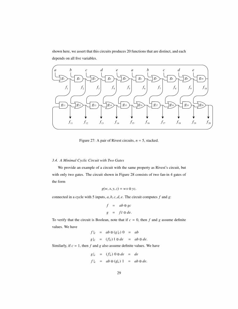
shown here, we assert that this circuits produces 20 functions that are distinct, and each
depends on all five variables.
g2g1 g4g3 g6g5 g8g7 g10g9
g12g11 g14g13 g16g15 g18g17 g20g19
1f
2f
3f
4f
5f
6f
7f
8f
9f
10f
11f
12f
13f
14f
15f
16f
17f
18f
19f
20f
a b c d e a b c d e
Figure 27: A pair of Rivest circuits, n = 5, stacked.
3.4. A Minimal Cyclic Circuit with Two Gates
We provide an example of a circuit with the same property as Rivest’s circuit, but
with only two gates. The circuit shown in Figure 28 consists of two fan-in 4 gates of
the form
g(w, x, y, z) = wx ⊕ yz.
connected in a cycle with 5 inputs, a, b, c, d, e. The circuit computes f and g:
f = ab ⊕ gc
g = f c ⊕ de.
To verify that the circuit is Boolean, note that if c = 0, then f and g assume definite
values. We havef |c = ab ⊕ (g |c) 0 = ab
g |c = ( f |c) 1 ⊕ de = ab ⊕ de.
Similarly, if c = 1, then f and g also assume definite values. We have
g |c = ( f |c) 0 ⊕ de = de
f |c = ab ⊕ (g|c) 1 = ab ⊕ de.
29
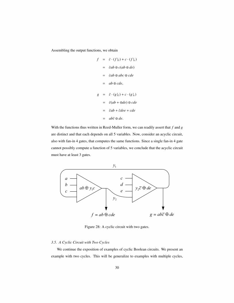
Assembling the output functions, we obtain
f = c · ( f |c) + c · ( f |c)
= cab ⊕ c(ab ⊕ de)
= cab ⊕ abc ⊕ cde
= ab ⊕ cde,
g = c · (g |c) + c · (g |c)
= c(ab + ⊕de) ⊕ cde
= cab + cdee + cde
= abc ⊕ de.
With the functions thus written in Reed-Muller form, we can readily assert that f and g
are distinct and that each depends on all 5 variables. Now, consider an acyclic circuit,
also with fan-in 4 gates, that computes the same functions. Since a single fan-in 4 gate
cannot possibly compute a function of 5 variables, we conclude that the acyclic circuit
must have at least 3 gates.
�
�
�
�
�
�
��
�����
������
�����
������
��
Figure 28: A cyclic circuit with two gates.
3.5. A Cyclic Circuit with Two Cycles
We continue the exposition of examples of cyclic Boolean circuits. We present an
example with two cycles. This will be generalize to examples with multiple cycles,
30

culminating with the main result of the paper: a cyclic circuit that is one-half the size
of any equivalent acyclic circuit.
Consider the circuit shown in Figure 29, written in a general form. The inputs are
x1, . . . , xn, grouped together in the figure as X. (A diagonal line across a wire indicates
that it represents multiple wires.) There are three gates, connected in a configuration
consisting of two cycles:
f1 = α1 ⊕ β1 f3
f2 = α2 ⊕ β2 f3
f3 = α3 ⊕ β3 f1 ⊕ γ3 f2 ⊕ δ3 f1 f2
where the α’s, β’s, γ’s, and δ’s are arbitrary functions of the input variables.
3111 ff βα ⊕=
X
X
X 213231333 fffff δγβα ⊕⊕⊕=
3222 ff βα ⊕=
nxxxX ,,, 21 K=Input variables:
1g
2g
3g
Figure 29: A cyclic circuit with two cycles.
We analyze this circuit with the goal of obtaining a necessary and sufficient con-
dition for it to be Boolean, as well as expressions for the gate outputs in terms of the
inputs. We proceed on a case-by-case basis. For what follows, when we speak of val-
ues of αi, βi, γi and δi, for i = 1, 2, 3, we mean the values evaluated at X.
31

Case I
Suppose that for some X, we have that β1 = 0. In this case f1 assumes the definite value
α1. This situation is shown in Figure 30. Now suppose further that γ3⊕δ3α1 = 0. In this
11 α=f
21331333 )( ff αδγαβα ⊕⊕⊕=
3222 ff βα ⊕=
X
X
X
1g
2g
3g
Figure 30: The circuit of Figure 29 if β1 = 0.
case, f3 assumes a definite value of α3 ⊕β3α1. Given this value for f3, it follows that f2
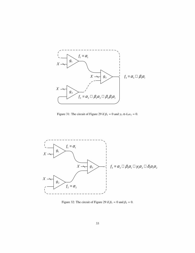
assumes the definite value of α2 ⊕ β2α3 ⊕ β2β3α1. This situation is shown in Figure 31.
We conclude that the functions assume definite values if β1 = 0 and γ3 ⊕ δ3α1 = 0.
Case II
Similarly, it can be shown that the functions f1, f2 and f3 assume definite values if
β2 = 0 and β3 ⊕ δ3α2 = 0.
Case III
Suppose that for some X, we have β1 = 0 and β2 = 0. In this case f1 and f2 assume
definite values of α1 and α2, respectively. Given these values for f1 and f2, it follows
that f3 assumes the definite value of α3⊕β3α1⊕γ3α2⊕δ3α1α2. This situation is shown
in Figure 32.
32
11 α=f
1333 αβα ⊕=f
1323222 αββαβα ⊕⊕=f
X
X
X
1g
2g
3g
Figure 31: The circuit of Figure 29 if β1 = 0 and γ3 ⊕ δ3α1 = 0.
11 α=f
213231333 ααδαγαβα ⊕⊕⊕=f
22 α=f
X
X
X
1g
2g
3g
Figure 32: The circuit of Figure 29 if β1 = 0 and β2 = 0.
33
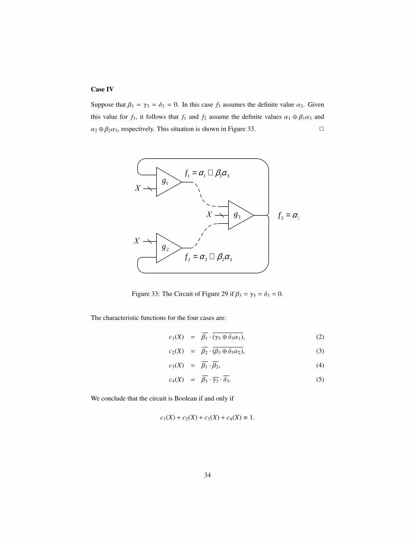
Case IV
Suppose that β3 = γ3 = δ3 = 0. In this case f3 assumes the definite value α3. Given
this value for f3, it follows that f1 and f2 assume the definite values α1 ⊕ β1α3 and
α2 ⊕ β2α3, respectively. This situation is shown in Figure 33. 2
3111 αβα ⊕=f
X
X
X 33 α=f
3222 αβα ⊕=f
1g
2g
3g
Figure 33: The Circuit of Figure 29 if β3 = γ3 = δ3 = 0.
The characteristic functions for the four cases are:
c1(X) = β1 · (γ3 ⊕ δ3α1), (2)
c2(X) = β2 · (β3 ⊕ δ3α2), (3)
c3(X) = β1 · β2, (4)
c4(X) = β3 · γ3 · δ3. (5)
We conclude that the circuit is Boolean if and only if
c1(X) + c2(X) + c3(X) + c4(X) ≡ 1.
34
If this condition holds, then the functions have values
f1(X) = c1α1 + c2(α1 ⊕ β1α3 ⊕ β1γ3α2) + c3α1 + c4(α1 ⊕ β1α3) (6)
f2(X) = c1(α2 ⊕ β2α3 ⊕ β1β3α1) + c2α2 + c3α2 + c4(α2 ⊕ β2α3) (7)
f3(X) = c1(α3 ⊕ β3α1) + c2(α3 ⊕ γ3α2) + c3(α3 ⊕ β3α1 ⊕ γ3α2δ3α1α2) + c4α3. (8)
3.6. A Circuit Three-Fifths the Size
Let’s make the circuit of Figure 29 somewhat more concrete. Suppose that the
inputs are a, b, x1, x2, . . . , xn, y1, y2, . . . , yn, z1, z2, . . . , zn. Suppose that the gates are de-
fined by
α1 = aX, α2 = bY, α3 = Z,
where
X = x1x2 · · · , xn, Y = y1y2 · · · , yn, Z = z1z2 · · · , zn
and
β1 = a, β2 = b, β3 = a,
γ3 = b, δ3 = ab.
The resulting circuit is shown in Figure 34. For this circuit, the conditions defined in
Equations 2– 5 evaluate to:
c1 = a(b + X),
c2 = b(a + Y),
c3 = ab,
c4 = ab.
It may easily be verified that for every combination of values assigned to a and b, one
of c1, c2, c3, c4 is true. The functions defined in Equations 6–8 are
f1(a, b, X,Y,Z) = X ⊕ a(X ⊕ Y ⊕ Z) ⊕ abY,
f2(a, b, X,Y,Z) = Y ⊕ b(X ⊕ Y ⊕ Z) ⊕ abX,
f3(a, b, X,Y,Z) = X ⊕ Y ⊕ Z ⊕ XY ⊕ a(X ⊕ XY) ⊕ b(Y ⊕ XY) ⊕ abXY.
35
31 faXaf ⊕=
21213 ffbafbfaZf ⊕⊕⊕=
32 fbYbf ⊕=
1g
2g
3g
)(21 n
xxxX
)(21 n
yyyY
)(21 n
zzzZ
K21, xxa
K21, xxb
K2,1,, zzba
Figure 34: Variant of the circuit of Figure 29.
With the functions expressed in Reed-Muller form, we can assert that they are dis-
tinct and that each depends on all the variables. To make the situation more concrete,
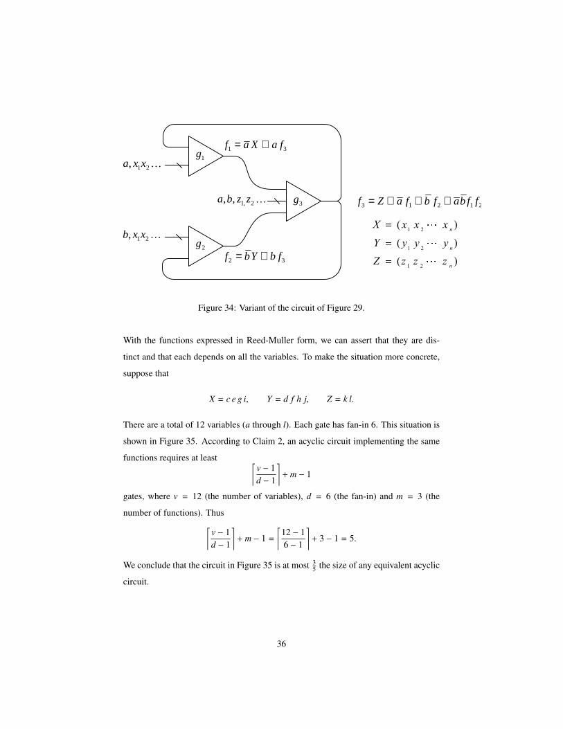
suppose that
X = c e g i, Y = d f h j, Z = k l.
There are a total of 12 variables (a through l). Each gate has fan-in 6. This situation is
shown in Figure 35. According to Claim 2, an acyclic circuit implementing the same
functions requires at least ⌈v − 1d − 1
⌉+ m − 1
gates, where v = 12 (the number of variables), d = 6 (the fan-in) and m = 3 (the
number of functions). Thus⌈v − 1d − 1
⌉+ m − 1 =
⌈12 − 16 − 1
⌉+ 3 − 1 = 5.
We conclude that the circuit in Figure 35 is at most 35 the size of any equivalent acyclic
circuit.
36

31 )( faigecaf ⊕=
a,c,e,g,i
b,d,f,h,j
a,b,k,l21213 ffbafbfak lf ⊕⊕⊕=
32 )( fbjhfdbf ⊕=
1g
2g
3g
Figure 35: Circuit of Figure 34 with 12 variables.
3.7. A Circuit One-Half the Size
Consider the circuit shown in Figure 36, a generalization of the circuit in Figure 29
to k gates. We argue the validity of this circuit informally. On the one hand, for each
variable xi, if xi = 0 then fi does not depend on fk+1. On the other hand, if xi = 1, then
fk+1 does not depend on fi. We conclude that none of the k cycles can be sensitized,
and so the circuit is Boolean. Now consider the function fi implemented by each gate.
With xi = 0, we see that fi depends on the variables y1,1, . . . , y1,d−1. Since fk+1 depends
on fi, it also depends on these variables. Thus fk+1 depends all the variables yi, j for
i = 1, . . . , k and j = 1, . . . , d − 1. With xi = 1, we see that fi depends on fk+1; hence it
also depends on all these variables. We conclude that each function depends on all the
variables.
With the fan-in of the gates set to d, the number of variables is
v = k(d − 1) + d − 2k = (k + 1)d − 3k
and the number of gates is
m = k + 1.
37

11111 +⊕= kfxYxf
1+⊕= kkkkk fxYxf
1g
kg
1+kg
)( 1 kdzzZ −= L
1,1, ,,, −dkkk yyx K
kdk zzxx −,,,,, 11 KK
12222 +⊕= kfxYxf
2g1,21,22 ,,, −dyyx K
kkkkk ffxxfxfxfxZf LLL 1122111 ⊕⊕⊕⊕⊕=+
1,11,11 ,,,, −dyyx K
1+kf
)( 1,11, −= dii yyY L ki ,,1
Figure 36: A generalization of the circuit of Figure 29.
38

According to Claim 2, an acyclic circuit implementing the same functions requires at
least ⌈v − 1d − 1
⌉+ m − 1
gates. The improvement factor is,
m⌈v−1d−1
⌉+ m − 1
=k + 1⌈
(k+1)d−3k−1d−1
⌉+ k=
k + 1⌈k + 1 − 2k
d−1
⌉+ k
gates. Suppose that d = 2k + 1 and that k is large. Then the ratio is
k + 12k≈
12.
We conclude that the circuit of Figure 36 is at most one-half the size of any equivalent
acyclic circuit. According to Claim 3, this is the best possible improvement factor that
we can obtain with the fan-in lower bound of Section 3.1.
39
4. Discussion
In related work, we have explored the practical implications of cyclic Boolean
circuits. We have described an efficient approach for analyzing cyclic circuits, and
we have provided a general framework for synthesizing such circuits. Our synthesis
tool, called CYCLIFY, is built within the Berkeley SIS and ABC environments (Sen-
tovich et al., 1992; Mishchenko et al., 2007). Timing analysis is performed with binary
decision diagrams (BDDs) and Boolean satisfiability (SAT)-based techniques (Riedel
and Bruck, 2003a, 2004; Backes et al., 2008). Synthesis is performed by introducing
cycles through the incremental application of restructuring and minimization opera-
tions (Riedel and Bruck, 2003b). We have explored the technique of Craig interpo-
lation for synthesizing cyclic functional dependencies (McMillan, 2003; Backes and
Riedel, 2009). Perhaps the most salient result to report is that cyclic solutions are not a
rarity. On trials with industry-accepted benchmark circuits, we improved the design of
many circuits significantly in terms of area and delay by introducing cycles.
In theoretical computer science, one of the main goals is to prove lower bounds on
the resources, such as time and space, required for computation. The Boolean circuit
model is often postulated as a representative model for computation with digital cir-
cuits. Unlike more abstract models of computation, such as Turing machines, Boolean
circuits can be viewed as bit-level implementation of a computational procedure – in
a sense, the most basic way that one can compute something. A lower bound on the
circuit size is taken as a true measure of the computational requirements of a problem.
For instance, lower bounds on circuit size have be used to justify the security of cryp-
tographic algorithms (Rothe, 2002). Complexity theorists invariably define a Boolean
circuit as a directed acyclic graph (DAG) (Papadimitriou, 1995, p. 80) and (Vollmer,
1999, p. 8). It is conceivable that some of the proofs of lower bounds on circuit size
depend on this definition.
We hope that this paper will help promulgate the view that a Boolean circuit is not
necessarily a DAG; rather it is a directed graph that may have cycles. This distinction
is a fundamental one. We have demonstrated that, both in theory and in practice, it is
not only feasible to design Boolean circuits with cyclic topologies, but this may well
be the best way to design them.
40
Backes, J., Fett, B., Riedel, M. D., 2008. The analysis of cyclic circuits with Boolean
satisfiability. In: International Conference on Computer-Aided Design. pp. 143–148.
Backes, J., Riedel, M. D., 2009. The synthesis of cyclic dependencies with Craig inter-
polation. In: International Workshop on Logic and Synthesis. pp. 24–30.
Brzozowski, J., Seger, C.-J., 1995. Asynchronous Circuits. Springer-Verlag.
Huffman, D. A., 1971. Combinational circuits with feedback. In: Mukhopadhyay, A.
(Ed.), Recent Developments in Switching Theory. Academic Press, pp. 27–55.
Katz, R., 1992. Contemporary Logic Design. Benjamin/Cummings.
Kautz, W. H., 1970. The necessity of closed circuit loops in minimal combinational
circuits. IEEE Transactions on Computers C-19 (2), 162–164.
Khrapchenko, V., 1978. Depth and delay in a network (in Russian). Soviet Mathematics
– Doklady 19, 1006–1009.
Markov, A., 1958. On the inversion complexity of a system of functions. Journal of the
ACM 5, 331–334.
McCaw, C., 1963. Loops in directed combinational switching networks. Ph.D. thesis,
Stanford University.
McMillan, K. L., 2003. Interpolation and SAT-based model checking. In: International
Conference on Computer Aided Verification. pp. 1–13.
Mishchenko, A., et al., 2007. ABC: A system for sequential synthesis and verification.
URL http://www.eecs.berkeley.edu/∼alanmi/abc/
Papadimitriou, C. H., 1995. Computational Complexity. Addison-Wesley.
Riedel, M. D., Bruck, J., 2003a. Cyclic combinational circuits: Analysis for synthesis.
In: International Workshop on Logic and Synthesis. pp. 105–112.
Riedel, M. D., Bruck, J., 2003b. The synthesis of cyclic combinational circuits. In:
Design Automation Conference. pp. 163–168.
41
Riedel, M. D., Bruck, J., 2004. Timing analysis of cyclic combinational circuits. In:
International Workshop on Logic and Synthesis.
Rivest, R. L., 1977. The necessity of feedback in minimal monotone combinational
circuits. IEEE Transactions on Computers 26 (6), 606–607.
Rothe, J., 2002. Some facets of complexity theory and cryptography. ACM Computing
Surveys 34 (4), 504–549.
Sentovich, E. M., et al., 1992. SIS: A system for sequential circuit synthesis. Tech. rep.,
University of California, Berkeley.
Shannon, C. E., 1949. The synthesis of two terminal switching circuits. Bell System
Technical Journal 28, 59–98.
Short, R., 1961. A theory of relations between sequential and combinational realiza-
tions of switching functions. Ph.D. thesis, Stanford University.
Vollmer, H., 1999. Introduction to Circuit Complexity. Springer.
Wakerly, J. F., 2000. Digital Design: Principles and Practices. Prentice-Hall.
Wegener, I., 1987. The Complexity of Boolean Functions. John Wiley & Sons.
Zhegalkin, I., 1929. The arithmetization of symbolic logic (in Russian). Matematich-
eskii Sbornik 36, 205–338.
42