cy7c65113c usb hub with microcontroller - farnell … · functional overview the cy7c65113c device...
TRANSCRIPT
CY7C65113C
USB Hub with Microcontroller
Cypress Semiconductor Corporation • 198 Champion Court • San Jose, CA 95134-1709 • 408-943-2600Document #: 38-08002 Rev. *G Revised March 21, 2014
Features■ Full Speed USB hub with an integrated microcontroller
■ 8-bit USB optimized microcontroller❐ Harvard architecture❐ 6-MHz external clock source❐ 12-MHz internal CPU clock❐ 48-MHz internal hub clock
■ Internal memory❐ 256 bytes of RAM❐ 8 KB of PROM
■ Integrated Master/Slave I2C-compatible Controller (100 kHz) enabled through General-purpose I/O (GPIO) pins
■ I/O ports❐ Two GPIO ports (Port 0 to 2) capable of sinking 7 mA per
pin (typical)❐ Higher current drive achievable by connecting multiple
GPIO pins together to drive a common output❐ Each GPIO port can be configured as inputs with internal
pull-ups or open drain outputs or traditional CMOS outputs❐ Maskable interrupts on all I/O pins
■ 12-bit free-running timer with one microsecond clock ticks
■ Watchdog timer (WDT)
■ Internal Power-on Reset (POR)
■ USB Specification compliance❐ Conforms to USB Specification, Version 1.1❐ Conforms to USB HID Specification, Version 1.1❐ Supports one or two device addresses with up to 5 us-
er-configured endpoints• Up to two 8-byte control endpoints• Up to four 8-byte data endpoints• Up to two 32-byte data endpoints
❐ Integrated USB transceivers❐ Supports four downstream USB ports❐ GPIO pins can provide individual power control outputs for
each downstream USB port❐ GPIO pins can provide individual port over current inputs
for each downstream USB port
■ Improved output drivers to reduce electromagnetic inter-ference (EMI)
■ Operating voltage from 4.0V to 5.5V DC
■ Operating temperature from 0° to 70° C
■ Available in 28-pin SOIC (-SXC) package
■ Industry-standard programmer support
CY7C65113C
Document #: 38-08002 Rev. *G Page 2 of 48
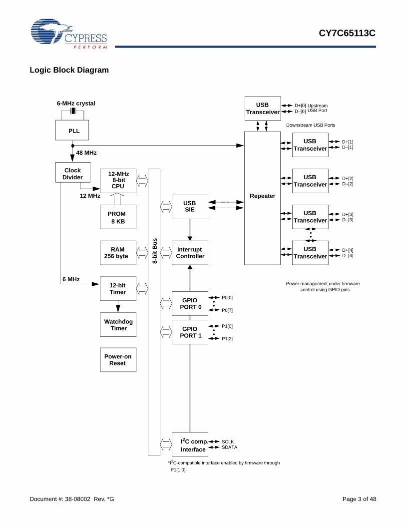
Functional OverviewThe CY7C65113C device is a one-time programmable 8-bit microcontroller with a built-in 12-Mbps USB hub that supports up to four downstream ports. The microcontroller instruction set has been optimized specifically for USB operations, although the microcontrollers can be used for a variety of non-USB embedded applications.GPIOThe CY7C65113C has 11 GPIO pins (P0[7:0], P1[2:0]), both rated at 7 mA per pin (typical) sink current. Multiple GPIO pins can be connected together to drive a single output for more drive current capacity.ClockThe microcontroller uses an external 6-MHz crystal and an internal oscillator to provide a reference to an internal phase-locked loop (PLL)-based clock generator. This technology allows the customer application to use an inexpensive 6-MHz fundamental crystal that reduces the clock-related noise emissions (EMI). A PLL clock generator provides the 6-, 12-, and 48-MHz clock signals for distribution within the microcontroller.MemoryThe CY7C65113C is offered with 8 KB of PROM.Power-on Reset, Watchdog, and Free-running Timer These parts include power-on reset logic, a Watchdog timer, and a 12-bit free-running timer. The POR logic detects when power is applied to the device, resets the logic to a known state, and begins executing instructions at PROM address 0x0000. The Watchdog timer is used to ensure the microcontroller recovers after a period of inactivity. The firmware may become inactive for a variety of reasons, including errors in the code or a hardware failure such as waiting for an interrupt that never occurs. I2CThe microcontroller can communicate with external electronics through the GPIO pins. An I2C-compatible interface accommo-dates a 100-kHz serial link with an external device.TimerThe free-running 12-bit timer clocked at 1 MHz provides two interrupt sources, 128-μs and 1.024-ms. The timer can be used
to measure the duration of an event under firmware control by reading the timer at the start of the event and after the event is complete. The difference between the two readings indicates the duration of the event in microseconds. The upper four bits of the timer are latched into an internal register when the firmware reads the lower eight bits. A read from the upper four bits actually reads data from the internal register, instead of the timer. This feature eliminates the need for firmware to try to compensate if the upper four bits increment immediately after the lower eight bits are read.InterruptsThe microcontroller supports ten maskable interrupts in the vectored interrupt controller. Interrupt sources include the USB Bus Reset interrupt, the 128-μs (bit 6) and 1.024-ms (bit 9) outputs from the free-running timer, five USB endpoints, the USB hub, the GPIO ports, and the I2C-compatible master mode interface. The timer bits cause an interrupt (if enabled) when the bit toggles from LOW ‘0’ to HIGH ‘1’. The USB endpoints interrupt after the USB host has written data to the endpoint FIFO or after the USB controller sends a packet to the USB host. The GPIO ports also have a level of masking to select which GPIO inputs can cause a GPIO interrupt. Input transition polarity can be programmed for each GPIO port as part of the port configuration. The interrupt polarity can be rising edge (‘0’ to ‘1’) or falling edge (‘1’ to ‘0’).USBThe CY7C65113C includes an integrated USB Serial Interface Engine (SIE) that supports the integrated peripherals and the hub controller function. The hardware supports up to two USB device addresses with one device address for the hub (two endpoints) and a device address for a compound device (three endpoints). The SIE allows the USB host to communicate with the hub and functions integrated into the microcontroller. The CY7C65113C part includes a 1:4 hub repeater with one upstream port and four downstream ports. The USB Hub allows power management control of the downstream ports by using GPIO pins assigned by the user firmware. The user has the option of ganging the downstream ports together with a single pair of power management pins, or providing power management for each port with four pairs of power management pins.
CY7C65113C
Document #: 38-08002 Rev. *G Page 3 of 48
Logic Block Diagram
InterruptController
PROM
12-bitTimer
Reset
WatchdogTimer
Repeater
Power-on
SCLKI2C comp.
USBTransceiver
USBTransceiver
USBTransceiver
GPIOPORT 1
GPIOPORT 0
P0[0]
P0[7]
P1[0]
P1[2]
SDATA
D+[3]D–[3]
D+[2]D–[2]
8-bi
t Bus
6-MHz crystal
RAM
USBSIE
USBTransceiver
D+[4]D–[4]
USBTransceiver
D+[0]D–[0]
D+[1]D–[1]
UpstreamUSB Port
256 byte
8 KB
Clock
6 MHz
12-MHz8-bitCPU
Power management under firmwarecontrol using GPIO pins
Interface
PLL
12 MHz
48 MHz
Divider
Downstream USB Ports
*I2C-compatible interface enabled by firmware throughP1[1:0]

CY7C65113C
Document #: 38-08002 Rev. *G Page 4 of 48
ContentsPin Configurations ........................................................... 5Product Summary Tables ................................................ 5Programming Model .........................................................8Clocking .......................................................................... 11Reset ................................................................................ 12Suspend Mode ................................................................ 13General-purpose I/O Ports ............................................. 1412-bit Free-Running Timer ............................................. 17I2C Configuration Register ............................................ 18I2C-compatible Controller .............................................. 18Processor Status and Control Register ....................... 20Interrupts ......................................................................... 21USB Overview ................................................................. 26USB Hub .......................................................................... 26USB Mode Tables ........................................................... 35Register Summary .......................................................... 39
Sample Schematic .......................................................... 41Absolute Maximum Ratings .......................................... 41Electrical Characteristics ............................................... 42Switching Characteristics .............................................. 43Ordering Information ...................................................... 44
Ordering Code Definitions ......................................... 44Package Diagram ............................................................ 45Acronyms ........................................................................ 46Document Conventions ................................................. 46
Units of Measure ....................................................... 46Document History Page ................................................. 47Sales, Solutions, and Legal Information ...................... 48
Worldwide Sales and Design Support ....................... 48Products .................................................................... 48PSoC Solutions ......................................................... 48

CY7C65113C
Document #: 38-08002 Rev. *G Page 5 of 48
Product Summary TablesPin Assignments
Pin ConfigurationsFigure 1. CY7C65113C 28-Pin SOIC
1
2
3
4
5
6
7
9
11
12
13
14
XTALIN
10
8
15
17
16
19
18
21
20
23
22
25
24
26
28
27
VCC
P1[1]
P1[0]
P1[2]
D–[3]
D+[3]
D–[4]
D+[4]
VREF
GND
D+[0]
D–[0]
D+[1]
D–[1]
D+[2]
D–[2]
P0[7]
P0[5]
P0[3]
P0[1]
XTALOUT
GND
VPP
P0[0]
P0[2]
P0[4]
P0[6]
Top View
Table 1. Pin Assignments
Name I/O 28-pin DescriptionD+[0], D–[0] I/O 5, 6 Upstream port, USB differential data.D+[1], D–[1] I/O 7, 8 Downstream Port 1, USB differential data.D+[2], D–[2] I/O 9, 10 Downstream Port 2, USB differential data.D+[3], D–[3] I/O 23, 24 Downstream Port 3, USB differential data.D+[4], D–[4] I/O 21, 22 Downstream Port 4, USB differential data.P0 I/O P1[7:0]
11, 15, 12, 16, 13, 17, 14, 18GPIO Port 0 capable of sinking 7 mA (typical).
P1 I/O P1[2:0]25, 27, 26
GPIO Port 1 capable of sinking 7 mA (typical).
XTALIN IN 2 6-MHz crystal or external clock input.XTALOUT OUT 1 6-MHz crystal out.VPP 19 Programming voltage supply, tie to ground during normal operation.VCC 28 Voltage supply.GND 4, 20 Ground.VREF IN 3 External 3.3V supply voltage for the downstream differential data output
buffers and the D+ pull-up.
CY7C65113C
Document #: 38-08002 Rev. *G Page 6 of 48
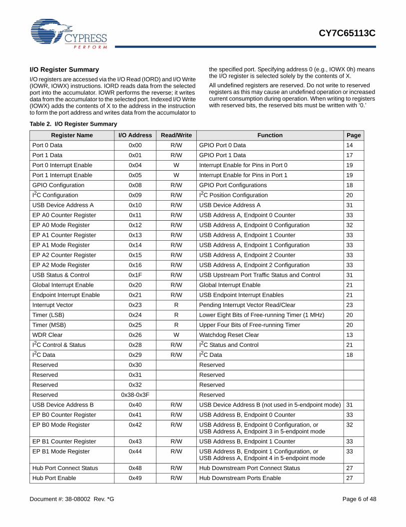
I/O Register SummaryI/O registers are accessed via the I/O Read (IORD) and I/O Write (IOWR, IOWX) instructions. IORD reads data from the selected port into the accumulator. IOWR performs the reverse; it writes data from the accumulator to the selected port. Indexed I/O Write (IOWX) adds the contents of X to the address in the instruction to form the port address and writes data from the accumulator to
the specified port. Specifying address 0 (e.g., IOWX 0h) means the I/O register is selected solely by the contents of X.All undefined registers are reserved. Do not write to reserved registers as this may cause an undefined operation or increased current consumption during operation. When writing to registers with reserved bits, the reserved bits must be written with ‘0.’
Table 2. I/O Register Summary
Register Name I/O Address Read/Write Function PagePort 0 Data 0x00 R/W GPIO Port 0 Data 14
Port 1 Data 0x01 R/W GPIO Port 1 Data 17
Port 0 Interrupt Enable 0x04 W Interrupt Enable for Pins in Port 0 19
Port 1 Interrupt Enable 0x05 W Interrupt Enable for Pins in Port 1 19
GPIO Configuration 0x08 R/W GPIO Port Configurations 18
I2C Configuration 0x09 R/W I2C Position Configuration 20
USB Device Address A 0x10 R/W USB Device Address A 31
EP A0 Counter Register 0x11 R/W USB Address A, Endpoint 0 Counter 33
EP A0 Mode Register 0x12 R/W USB Address A, Endpoint 0 Configuration 32
EP A1 Counter Register 0x13 R/W USB Address A, Endpoint 1 Counter 33
EP A1 Mode Register 0x14 R/W USB Address A, Endpoint 1 Configuration 33
EP A2 Counter Register 0x15 R/W USB Address A, Endpoint 2 Counter 33
EP A2 Mode Register 0x16 R/W USB Address A, Endpoint 2 Configuration 33
USB Status & Control 0x1F R/W USB Upstream Port Traffic Status and Control 31
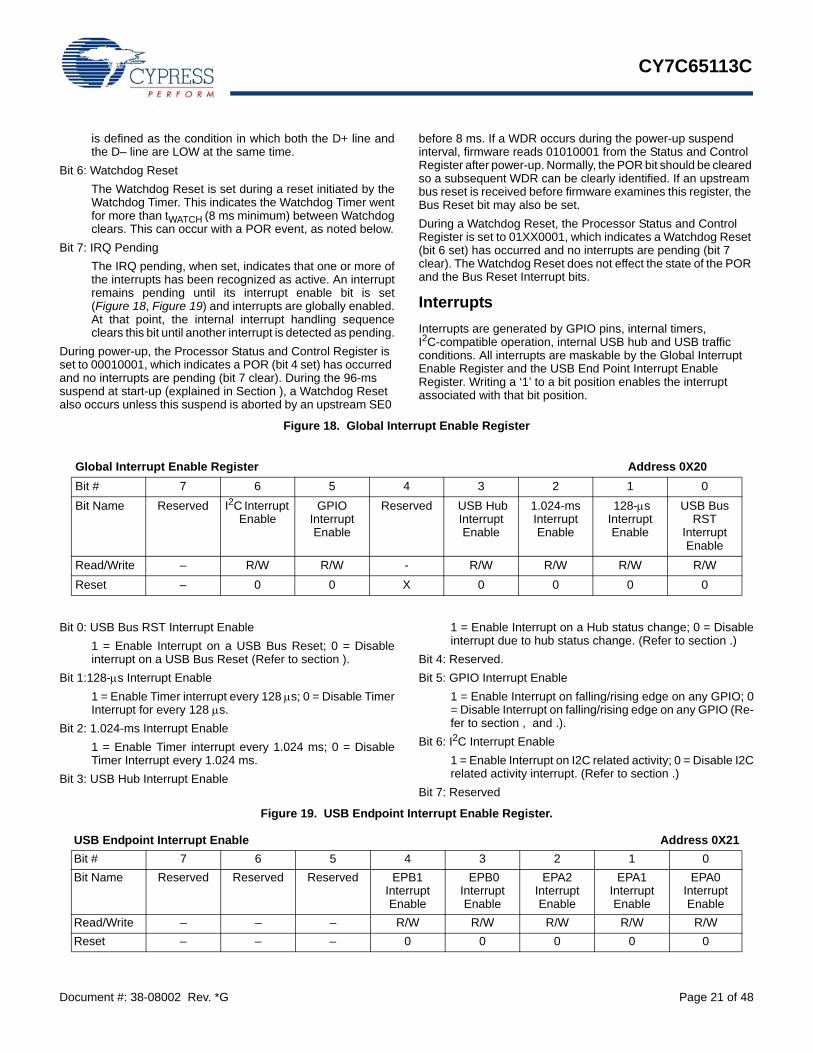
Global Interrupt Enable 0x20 R/W Global Interrupt Enable 21
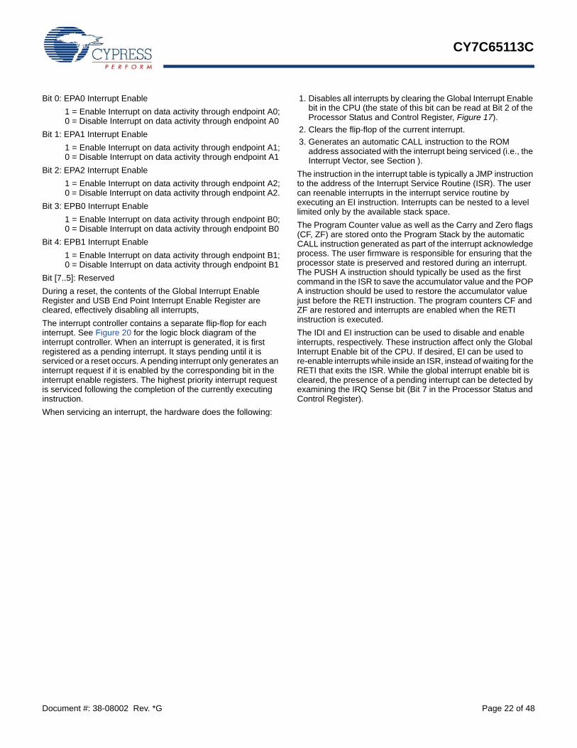
Endpoint Interrupt Enable 0x21 R/W USB Endpoint Interrupt Enables 21
Interrupt Vector 0x23 R Pending Interrupt Vector Read/Clear 23
Timer (LSB) 0x24 R Lower Eight Bits of Free-running Timer (1 MHz) 20
Timer (MSB) 0x25 R Upper Four Bits of Free-running Timer 20
WDR Clear 0x26 W Watchdog Reset Clear 13
I2C Control & Status 0x28 R/W I2C Status and Control 21
I2C Data 0x29 R/W I2C Data 18
Reserved 0x30 Reserved
Reserved 0x31 Reserved
Reserved 0x32 Reserved
Reserved 0x38-0x3F Reserved
USB Device Address B 0x40 R/W USB Device Address B (not used in 5-endpoint mode) 31
EP B0 Counter Register 0x41 R/W USB Address B, Endpoint 0 Counter 33
EP B0 Mode Register 0x42 R/W USB Address B, Endpoint 0 Configuration, or USB Address A, Endpoint 3 in 5-endpoint mode
32
EP B1 Counter Register 0x43 R/W USB Address B, Endpoint 1 Counter 33
EP B1 Mode Register 0x44 R/W USB Address B, Endpoint 1 Configuration, or USB Address A, Endpoint 4 in 5-endpoint mode
33
Hub Port Connect Status 0x48 R/W Hub Downstream Port Connect Status 27
Hub Port Enable 0x49 R/W Hub Downstream Ports Enable 27
CY7C65113C
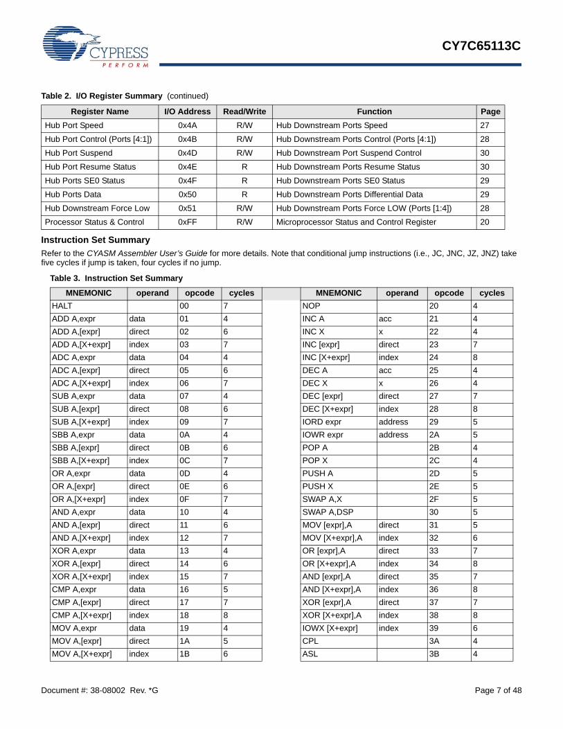
Document #: 38-08002 Rev. *G Page 7 of 48
Instruction Set SummaryRefer to the CYASM Assembler User’s Guide for more details. Note that conditional jump instructions (i.e., JC, JNC, JZ, JNZ) take five cycles if jump is taken, four cycles if no jump.
Hub Port Speed 0x4A R/W Hub Downstream Ports Speed 27
Hub Port Control (Ports [4:1]) 0x4B R/W Hub Downstream Ports Control (Ports [4:1]) 28
Hub Port Suspend 0x4D R/W Hub Downstream Port Suspend Control 30
Hub Port Resume Status 0x4E R Hub Downstream Ports Resume Status 30
Hub Ports SE0 Status 0x4F R Hub Downstream Ports SE0 Status 29
Hub Ports Data 0x50 R Hub Downstream Ports Differential Data 29
Hub Downstream Force Low 0x51 R/W Hub Downstream Ports Force LOW (Ports [1:4]) 28
Processor Status & Control 0xFF R/W Microprocessor Status and Control Register 20
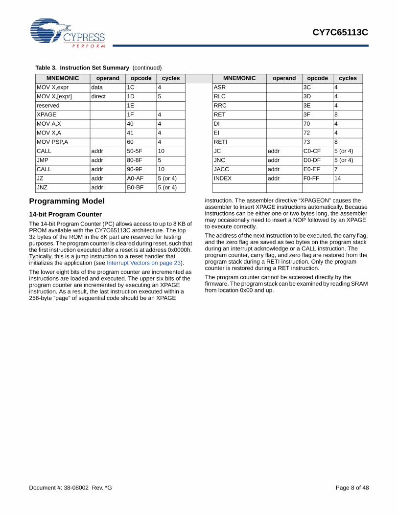
Table 3. Instruction Set Summary
MNEMONIC operand opcode cycles MNEMONIC operand opcode cyclesHALT 00 7 NOP 20 4ADD A,expr data 01 4 INC A acc 21 4ADD A,[expr] direct 02 6 INC X x 22 4ADD A,[X+expr] index 03 7 INC [expr] direct 23 7ADC A,expr data 04 4 INC [X+expr] index 24 8ADC A,[expr] direct 05 6 DEC A acc 25 4ADC A,[X+expr] index 06 7 DEC X x 26 4SUB A,expr data 07 4 DEC [expr] direct 27 7SUB A,[expr] direct 08 6 DEC [X+expr] index 28 8SUB A,[X+expr] index 09 7 IORD expr address 29 5SBB A,expr data 0A 4 IOWR expr address 2A 5SBB A,[expr] direct 0B 6 POP A 2B 4SBB A,[X+expr] index 0C 7 POP X 2C 4OR A,expr data 0D 4 PUSH A 2D 5OR A,[expr] direct 0E 6 PUSH X 2E 5OR A,[X+expr] index 0F 7 SWAP A,X 2F 5AND A,expr data 10 4 SWAP A,DSP 30 5AND A,[expr] direct 11 6 MOV [expr],A direct 31 5AND A,[X+expr] index 12 7 MOV [X+expr],A index 32 6XOR A,expr data 13 4 OR [expr],A direct 33 7XOR A,[expr] direct 14 6 OR [X+expr],A index 34 8XOR A,[X+expr] index 15 7 AND [expr],A direct 35 7CMP A,expr data 16 5 AND [X+expr],A index 36 8CMP A,[expr] direct 17 7 XOR [expr],A direct 37 7CMP A,[X+expr] index 18 8 XOR [X+expr],A index 38 8MOV A,expr data 19 4 IOWX [X+expr] index 39 6MOV A,[expr] direct 1A 5 CPL 3A 4MOV A,[X+expr] index 1B 6 ASL 3B 4
Table 2. I/O Register Summary (continued)
Register Name I/O Address Read/Write Function Page
CY7C65113C
Document #: 38-08002 Rev. *G Page 8 of 48
Programming Model14-bit Program CounterThe 14-bit Program Counter (PC) allows access to up to 8 KB of PROM available with the CY7C65113C architecture. The top 32 bytes of the ROM in the 8K part are reserved for testing purposes. The program counter is cleared during reset, such that the first instruction executed after a reset is at address 0x0000h. Typically, this is a jump instruction to a reset handler that initializes the application (see Interrupt Vectors on page 23).The lower eight bits of the program counter are incremented as instructions are loaded and executed. The upper six bits of the program counter are incremented by executing an XPAGE instruction. As a result, the last instruction executed within a 256-byte “page” of sequential code should be an XPAGE
instruction. The assembler directive “XPAGEON” causes the assembler to insert XPAGE instructions automatically. Because instructions can be either one or two bytes long, the assembler may occasionally need to insert a NOP followed by an XPAGE to execute correctly.The address of the next instruction to be executed, the carry flag, and the zero flag are saved as two bytes on the program stack during an interrupt acknowledge or a CALL instruction. The program counter, carry flag, and zero flag are restored from the program stack during a RETI instruction. Only the program counter is restored during a RET instruction.The program counter cannot be accessed directly by the firmware. The program stack can be examined by reading SRAM from location 0x00 and up.
MOV X,expr data 1C 4 ASR 3C 4MOV X,[expr] direct 1D 5 RLC 3D 4reserved 1E RRC 3E 4XPAGE 1F 4 RET 3F 8MOV A,X 40 4 DI 70 4MOV X,A 41 4 EI 72 4MOV PSP,A 60 4 RETI 73 8CALL addr 50-5F 10 JC addr C0-CF 5 (or 4)JMP addr 80-8F 5 JNC addr D0-DF 5 (or 4)CALL addr 90-9F 10 JACC addr E0-EF 7JZ addr A0-AF 5 (or 4) INDEX addr F0-FF 14JNZ addr B0-BF 5 (or 4)
Table 3. Instruction Set Summary (continued)
MNEMONIC operand opcode cycles MNEMONIC operand opcode cycles
CY7C65113C
Document #: 38-08002 Rev. *G Page 9 of 48
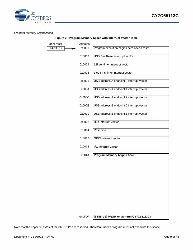
Program Memory Organization
Figure 2. Program Memory Space with Interrupt Vector Table
Note that the upper 32 bytes of the 8K PROM are reserved. Therefore, user’s program must not overwrite this space.
after reset Address 14-bit PC 0x0000 Program execution begins here after a reset
0x0002 USB Bus Reset interrupt vector
0x0004 128-μs timer interrupt vector
0x0006 1.024-ms timer interrupt vector
0x0008 USB address A endpoint 0 interrupt vector
0x000A USB address A endpoint 1 interrupt vector
0x000C USB address A endpoint 2 interrupt vector
0x000E USB address B endpoint 0 interrupt vector
0x0010 USB address B endpoint 1 interrupt vector
0x0012 Hub interrupt vector
0x0014 Reserved
0x0016 GPIO interrupt vector
0x0018 I2C interrupt vector
0x001A Program Memory begins here
0x1FDF (8 KB -32) PROM ends here (CY7C65113C)

CY7C65113C
Document #: 38-08002 Rev. *G Page 10 of 48
8-bit Accumulator (A)The accumulator is the general-purpose register for the micro-controller.
8-bit Temporary Register (X)The “X” register is available to the firmware for temporary storage of intermediate results. The microcontroller can perform indexed operations based on the value in X. Refer to Section for additional information.
8-bit Program Stack Pointer (PSP)During a reset, the Program Stack Pointer (PSP) is set to 0x00 and “grows” upward from this address. The PSP may be set by firmware, using the MOV PSP,A instruction. The PSP supports interrupt service under hardware control and CALL, RET, and RETI instructions under firmware control. The PSP is not readable by the firmware.During an interrupt acknowledge, interrupts are disabled and the 14-bit program counter, carry flag, and zero flag are written as two bytes of data memory. The first byte is stored in the memory addressed by the PSP, then the PSP is incremented. The second byte is stored in memory addressed by the PSP, and the PSP is incremented again. The overall effect is to store the program
counter and flags on the program “stack” and increment the PSP by two.The Return From Interrupt (RETI) instruction decrements the PSP, then restores the second byte from memory addressed by the PSP. The PSP is decremented again and the first byte is restored from memory addressed by the PSP. After the program counter and flags have been restored from stack, the interrupts are enabled. The overall effect is to restore the program counter and flags from the program stack, decrement the PSP by two, and re-enable interrupts.The Call Subroutine (CALL) instruction stores the program counter and flags on the program stack and increments the PSP by two.The Return From Subroutine (RET) instruction restores the program counter but not the flags from the program stack and decrements the PSP by two.
Data Memory OrganizationThe CY7C65113C microcontrollers provide 256 bytes of data RAM. Normally, the SRAM is partitioned into four areas: program stack, user variables, data stack, and USB endpoint FIFOs. The following is one example of where the program stack, data stack, and user variables areas could be located.
Notes1. Refer to Section for a description of DSP.2. Endpoint sizes are fixed by the Endpoint Size Bit (I/O register 0x1F, Bit 7). See Table 10.
After reset Address8-bit DSP 8-bit PSP 0x00 Program Stack Growth
(Move DSP[1])
8-bit DSP user selected Data Stack Growth
User variables
USB FIFO space for up to two Addresses and five endpoints[2]
0xFF
CY7C65113C
Document #: 38-08002 Rev. *G Page 11 of 48
8-bit Data Stack Pointer (DSP)The Data Stack Pointer (DSP) supports PUSH and POP instruc-tions that use the data stack for temporary storage. A PUSH instruction pre-decrements the DSP, then writes data to the memory location addressed by the DSP. A POP instruction reads data from the memory location addressed by the DSP, then post-increments the DSP. During a reset, the DSP is reset to 0x00. A PUSH instruction when DSP equals 0x00 writes data at the top of the data RAM (address 0xFF). This writes data to the memory area reserved for USB endpoint FIFOs. Therefore, the DSP should be indexed at an appropriate memory location that does not compromise the Program Stack, user-defined memory (variables), or the USB endpoint FIFOs.For USB applications, the firmware should set the DSP to an appropriate location to avoid a memory conflict with RAM dedicated to USB FIFOs. The memory requirements for the USB endpoints are described in Section 17.2. Example assembly instructions to do this with two device addresses (FIFOs begin at 0xD8) are shown below:
MOV A,20h ; Move 20 hex into Accumulator (must be D8hor less)SWAP A,DSP ; swap accumulator value into DSP register.
Address ModesThe CY7C65113 microcontrollers support three addressing modes for instructions that require data operands: data, direct, and indexed.
Data (Immediate)“Data” address mode refers to a data operand that is actually a constant encoded in the instruction. As an example, consider the instruction that loads A with the constant 0xD8:• MOV A, 0D8h.
This instruction requires two bytes of code where the first byte identifies the “MOV A” instruction with a data operand as the
second byte. The second byte of the instruction is the constant “0xD8.” A constant may be referred to by name if a prior “EQU” statement assigns the constant value to the name. For example, the following code is equivalent to the example shown above:• DSPINIT: EQU 0D8h• MOV A, DSPINIT.
Direct“Direct” address mode is used when the data operand is a variable stored in SRAM. In that case, the one byte address of the variable is encoded in the instruction. As an example, consider an instruction that loads A with the contents of memory address location 0x10:• MOV A, [10h].
Normally, variable names are assigned to variable addresses using “EQU” statements to improve the readability of the assembler source code. As an example, the following code is equivalent to the example shown above:• buttons: EQU 10h• MOV A, [buttons].
Indexed“Indexed” address mode allows the firmware to manipulate arrays of data stored in SRAM. The address of the data operand is the sum of a constant encoded in the instruction and the contents of the “X” register. Normally, the constant is the “base” address of an array of data and the X register contains an index that indicates which element of the array is actually addressed:• array: EQU 10h• MOV X, 3• MOV A, [X+array].
This would have the effect of loading A with the fourth element of the SRAM “array” that begins at address 0x10. The fourth element would be at address 0x13.
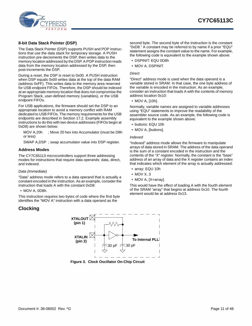
Clocking
XTALOUT
XTALIN To Internal PLL30 pF 30 pF
(pin 1)
(pin 2)
Figure 3. Clock Oscillator On-Chip Circuit
CY7C65113C
Document #: 38-08002 Rev. *G Page 12 of 48
The XTALIN and XTALOUT are the clock pins to the microcon-troller. The user can connect an external oscillator or a crystal to these pins. When using an external crystal, keep PCB traces between the chip leads and crystal as short as possible (less than 2 cm). A 6-MHz fundamental frequency parallel resonant crystal can be connected to these pins to provide a reference frequency for the internal PLL. The two internal 30-pF load caps appear in series to the external crystal and would be equivalent to a 15-pF load. Therefore, the crystal must have a required load capacitance of about 15–18 pF. A ceramic resonator does not allow the microcontroller to meet the timing specifications of full speed USB and therefore a ceramic resonator is not recom-mended with these parts.An external 6-MHz clock can be applied to the XTALIN pin if the XTALOUT pin is left open. Grounding the XTALOUT pin when driving XTALIN with an oscillator does not work because the internal clock is effectively shorted to ground.
ResetThe CY7C65113C supports two resets: POR and WDR. Each of these resets causes:• all registers to be restored to their default states• the USB device addresses to be set to 0• all interrupts to be disabled• the PSP and DSP to be set to memory address 0x00.
The occurrence of a reset is recorded in the Processor Status and Control Register, as described in Section. Bits 4 and 6 are used to record the occurrence of POR and WDR respectively. Firmware can interrogate these bits to determine the cause of a reset.
Program execution starts at ROM address 0x0000 after a reset. Although this looks like interrupt vector 0, there is an important difference. Reset processing does NOT push the program counter, carry flag, and zero flag onto program stack. The firmware reset handler should configure the hardware before the “main” loop of code. Attempting to execute a RET or RETI in the firmware reset handler causes unpredictable execution results.
Power-on ResetWhen VCC is first applied to the chip, the POR signal is asserted and the CY7C65113C enters a “semi-suspend” state. During the semi-suspend state, which is different from the suspend state defined in the USB specification, the oscillator and all other blocks of the part are functional, except for the CPU. This semi-suspend time ensures that both a valid VCC level is reached and that the internal PLL has time to stabilize before full operation begins. When the VCC has risen above approximately 2.5V, and the oscillator is stable, the POR is deasserted and the on-chip timer starts counting. The first 1 ms of suspend time is not interruptible, and the semi-suspend state continues for an additional 95 ms unless the count is bypassed by a USB Bus Reset on the upstream port. The 95 ms provides time for VCC to stabilize at a valid operating voltage before the chip executes code.If a USB Bus Reset occurs on the upstream port during the 95 ms semi-suspend time, the semi-suspend state is aborted and program execution begins immediately from address 0x0000. In this case, the Bus Reset interrupt is pending but not serviced until firmware sets the USB Bus Reset Interrupt Enable bit (Bit 0, Figure 18) and enables interrupts with the EI command. The POR signal is asserted whenever VCC drops below approx-imately 2.5V, and remains asserted until VCC rises above this level again. Behavior is the same as described above.
CY7C65113C
Document #: 38-08002 Rev. *G Page 13 of 48
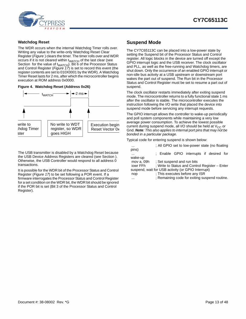
Watchdog ResetThe WDR occurs when the internal Watchdog Timer rolls over. Writing any value to the write-only Watchdog Reset Clear Register (Figure ) clears the timer. The timer rolls over and WDR occurs if it is not cleared within tWATCH of the last clear (see Section for the value of tWATCH). Bit 6 of the Processor Status and Control Register (Figure 17) is set to record this event (the register contents are set to 010X0001 by the WDR). A Watchdog Timer Reset lasts for 2 ms, after which the microcontroller begins execution at ROM address 0x0000.
Figure 4. Watchdog Reset (Address 0x26)
The USB transmitter is disabled by a Watchdog Reset because the USB Device Address Registers are cleared (see Section ). Otherwise, the USB Controller would respond to all address 0 transactions.It is possible for the WDR bit of the Processor Status and Control Register (Figure 17) to be set following a POR event. If a firmware interrogates the Processor Status and Control Register for a set condition on the WDR bit, the WDR bit should be ignored if the POR bit is set (Bit 3 of the Processor Status and Control Register).
Suspend ModeThe CY7C65113C can be placed into a low-power state by setting the Suspend bit of the Processor Status and Control register. All logic blocks in the device are turned off except the GPIO interrupt logic and the USB receiver. The clock oscillator and PLL, as well as the free-running and Watchdog timers, are shut down. Only the occurrence of an enabled GPIO interrupt or non-idle bus activity at a USB upstream or downstream port wakes the part out of suspend. The Run bit in the Processor Status and Control Register must be set to resume a part out of suspend.The clock oscillator restarts immediately after exiting suspend mode. The microcontroller returns to a fully functional state 1 ms after the oscillator is stable. The microcontroller executes the instruction following the I/O write that placed the device into suspend mode before servicing any interrupt requests.The GPIO interrupt allows the controller to wake-up periodically and poll system components while maintaining a very low average power consumption. To achieve the lowest possible current during suspend mode, all I/O should be held at VCC or Gnd. Note: This also applies to internal port pins that may not be bonded in a particular package.Typical code for entering suspend is shown below:
... ; All GPIO set to low-power state (no floatingpins)... ; Enable GPIO interrupts if desired forwake-upmov a, 09h ; Set suspend and run bits iowr FFh ; Write to Status and Control Register – Entersuspend, wait for USB activity (or GPIO Interrupt)nop ; This executes before any ISR... ; Remaining code for exiting suspend routine.
write to chdog Timerster
No write to WDTregister, so WDRgoes HIGH
Execution beginReset Vector 0x
tWATCH 2 ms
CY7C65113C
Document #: 38-08002 Rev. *G Page 14 of 48
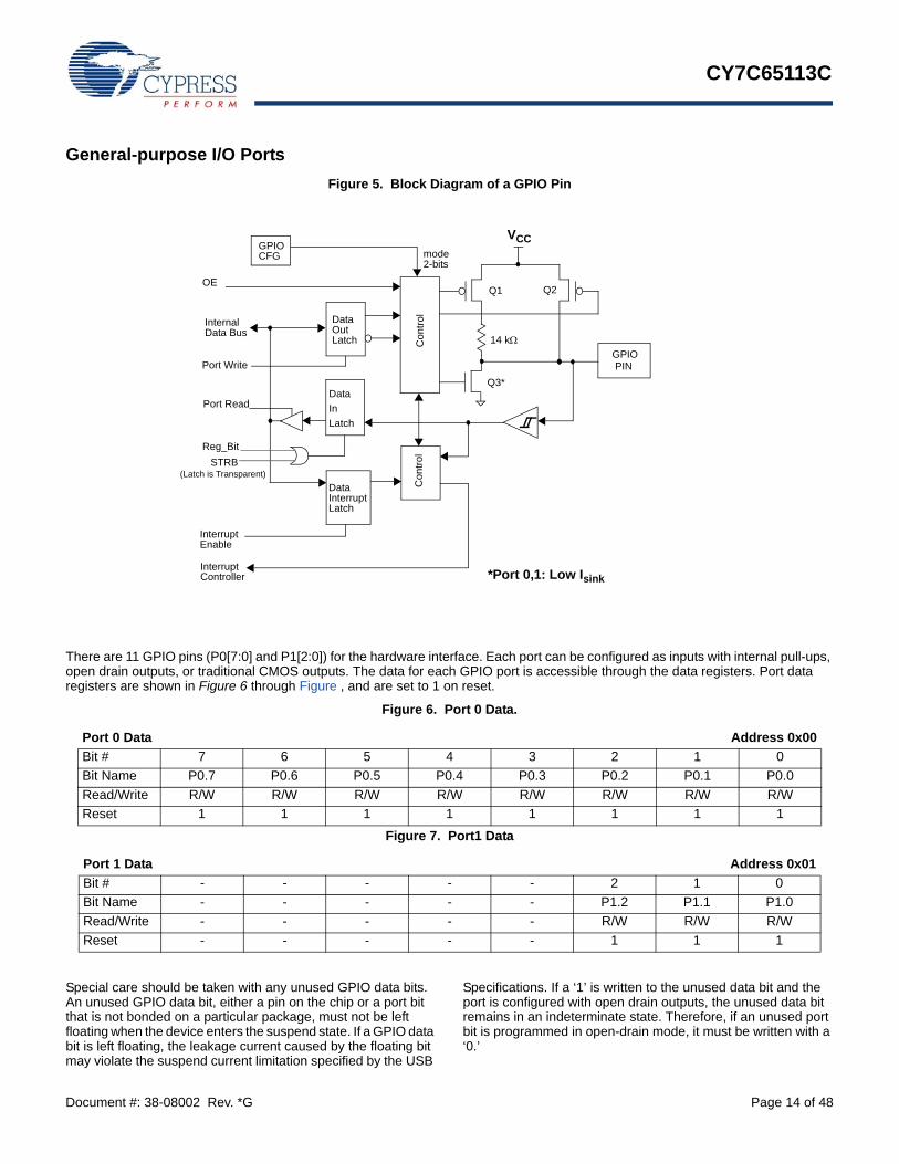
General-purpose I/O PortsFigure 5. Block Diagram of a GPIO Pin
There are 11 GPIO pins (P0[7:0] and P1[2:0]) for the hardware interface. Each port can be configured as inputs with internal pull-ups, open drain outputs, or traditional CMOS outputs. The data for each GPIO port is accessible through the data registers. Port data registers are shown in Figure 6 through Figure , and are set to 1 on reset.
Figure 6. Port 0 Data.
Special care should be taken with any unused GPIO data bits. An unused GPIO data bit, either a pin on the chip or a port bit that is not bonded on a particular package, must not be left floating when the device enters the suspend state. If a GPIO data bit is left floating, the leakage current caused by the floating bit may violate the suspend current limitation specified by the USB
Specifications. If a ‘1’ is written to the unused data bit and the port is configured with open drain outputs, the unused data bit remains in an indeterminate state. Therefore, if an unused port bit is programmed in open-drain mode, it must be written with a ‘0.’
Port 0 Data Address 0x00Bit # 7 6 5 4 3 2 1 0Bit Name P0.7 P0.6 P0.5 P0.4 P0.3 P0.2 P0.1 P0.0Read/Write R/W R/W R/W R/W R/W R/W R/W R/WReset 1 1 1 1 1 1 1 1
Figure 7. Port1 Data
Port 1 Data Address 0x01Bit # - - - - - 2 1 0Bit Name - - - - - P1.2 P1.1 P1.0Read/Write - - - - - R/W R/W R/WReset - - - - - 1 1 1
GPIO
VCC
14 kΩ
GPIOCFG mode
2-bits
DataOutLatch
InternalData Bus
Port Read
Port Write
InterruptEnable
Con
trol
Con
trol
InterruptController
Q1
Q3*
Q2
*Port 0,1: Low Isink
DataInterruptLatch
OE
Reg_BitSTRB
DataInLatch
(Latch is Transparent)
PIN

CY7C65113C
Document #: 38-08002 Rev. *G Page 15 of 48
A read from a GPIO port always returns the present state of the voltage at the pin, independent of the settings in the Port Data Registers. During reset, all of the GPIO pins are set to a high-impedance input state. Writing a ‘0’ to a GPIO pin drives the pin LOW. In this state, a ‘0’ is always read on that GPIO pin unless an external source overdrives the internal pull-down device.
GPIO Configuration PortEvery GPIO port can be programmed as inputs with internal pull-ups, outputs LOW or HIGH, or Hi-Z (floating, the pin is not driven internally). In addition, the interrupt polarity for each port can be programmed. The Port Configuration bits (Figure ) and the Interrupt Enable bit (Figure 10 through Figure 10) determine the interrupt polarity of the port pins
Figure 8. GPIO Configuration Register.
As shown in Table 4 below, a positive polarity on an input pin represents a rising edge interrupt (LOW to HIGH), and a negative polarity on an input pin represents a falling edge interrupt (HIGH to LOW).The GPIO interrupt is generated when all of the following condi-tions are met: the Interrupt Enable bit of the associated Port Interrupt Enable Register is enabled, the GPIO Interrupt Enable bit of the Global Interrupt Enable Register (Figure 18) is enabled, the Interrupt Enable Sense (bit 2, Figure 17) is set, and the GPIO pin of the port sees an event matching the interrupt polarity.
The driving state of each GPIO pin is determined by the value written to the pin’s Data Register (Figure 6 through Figure ) and by its associated Port Configuration bits as shown in the GPIO Configuration Register (Figure ). These ports are configured on a per-port basis, so all pins in a given port are configured together. The possible port configurations are detailed in Table 4. As shown in this table below, when a GPIO port is configured with CMOS outputs, interrupts from that port are disabled.During reset, all of the bits in the GPIO Configuration Register are written with ‘0’ to select Hi-Z mode for all GPIO ports as the default configuration.
GPIO Configuration Address 0x08Bit # 7 6 5 4 3 2 1 0Bit Name Reserved Reserved Reserved Reserved Port 1
Config Bit 1Port 1
Config Bit 0Port 0
Config Bit 1Port 0
Config Bit 0Read/Write - - - - R/W R/W R/W R/WReset - - - - 0 0 0 0
CY7C65113C
Document #: 38-08002 Rev. *G Page 16 of 48
Q1, Q2, and Q3 discussed below are the transistors referenced in Figure . The available GPIO drive strength are:
■ Output LOW Mode: The pin’s Data Register is set to ‘0.’Writing ‘0’ to the pin’s Data Register puts the pin in outputLOW mode, regardless of the contents of the Port Configura-tion Bits[1:0]. In this mode, Q1 and Q2 are OFF. Q3 is ON.The GPIO pin is driven LOW through Q3.
■ Output HIGH Mode: The pin’s Data Register is set to 1 and the Port Configuration Bits[1:0] is set to ‘10.’In this mode, Q1 and Q3 are OFF. Q2 is ON. The GPIO ispulled up through Q2. The GPIO pin is capable of sourcing...of current.
■ Resistive Mode: The pin’s Data Register is set to 1 and the Port Configuration Bits[1:0] is set to ‘11.’Q2 and Q3 are OFF. Q1 is ON. The GPIO pin is pulled up withan internal 14kΩ resistor. In resistive mode, the pin may serve
as an input. Reading the pin’s Data Register returns a logicHIGH if the pin is not driven LOW by an external source.
■ Hi-Z Mode: The pin’s Data Register is set to1 and Port Config-uration Bits[1:0] is set either ‘00’ or ‘01.’Q1, Q2, and Q3 are all OFF. The GPIO pin is not driven inter-nally. In this mode, the pin may serve as an input. Readingthe Port Data Register returns the actual logic value on theport pins.
GPIO Interrupt Enable PortsEach GPIO pin can be individually enabled or disabled as an interrupt source. The Port 0–1 Interrupt Enable Registers provide this feature with an Interrupt Enable bit for each GPIO pin.During a reset, GPIO interrupts are disabled by clearing all of the GPIO Interrupt Enable bits. Writing a ‘1’ to a GPIO Interrupt Enable bit enables GPIO interrupts from the corresponding input pin. All GPIO pins share a common interrupt, as discussed in Section .
Figure 9. . Port 0 Interrupt Enable
Table 4. GPIO Port Output Control Truth Table and Interrupt Polarity
Port Config Bit 1 Port Config Bit 0 Data Register Output Drive Strength Interrupt Enable Bit Interrupt Polarity1 1 0 Output LOW 0 Disabled
1 Resistive 1 – (Falling Edge)1 0 0 Output LOW 0 Disabled
1 Output HIGH 1 Disabled0 1 0 Output LOW 0 Disabled
1 Hi-Z 1 – (Falling Edge)0 0 0 Output LOW 0 Disabled
1 Hi-Z 1 + (Rising Edge)
Port 0 Interrupt Enable Address 0x04Bit # 7 6 5 4 3 2 1 0Bit Name P0.7 Intr
EnableP0.6 Intr Enable
P0.5 Intr Enable
P0.4 Intr Enable
P0.3 Intr Enable
P0.2 Intr Enable
P0.1 Intr Enable
P0.0 Intr Enable
Read/Write W W W W W W W WReset 0 0 0 0 0 0 0 0
Figure 10. Port 1 Interrupt Enable
Port 1 Interrupt Enable Address 0x05Bit # 7 6 5 4 3 2 1 0Bit Name Reserved Reserved Reserved Reserved Reserved P0.2 Intr
EnableP1.1 Intr Enable
P1.0 Intr Enable
Read/Write - - - - - W W WReset - - - - - 0 0 0
CY7C65113C
Document #: 38-08002 Rev. *G Page 17 of 48
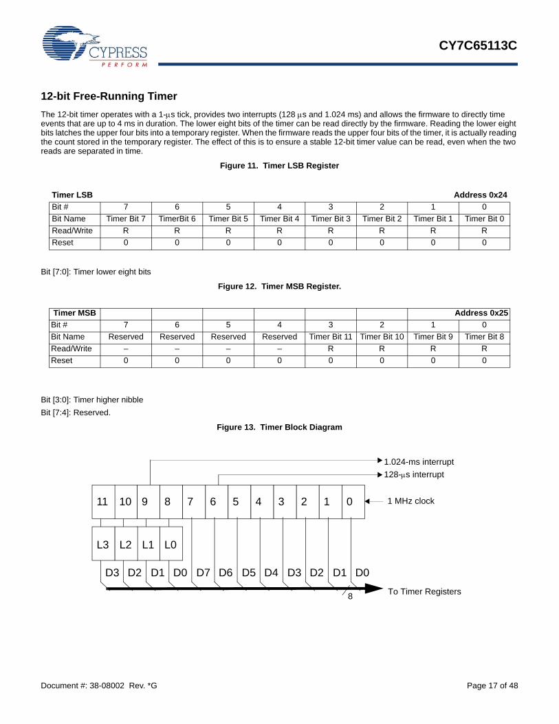
12-bit Free-Running TimerThe 12-bit timer operates with a 1-μs tick, provides two interrupts (128 μs and 1.024 ms) and allows the firmware to directly time events that are up to 4 ms in duration. The lower eight bits of the timer can be read directly by the firmware. Reading the lower eight bits latches the upper four bits into a temporary register. When the firmware reads the upper four bits of the timer, it is actually reading the count stored in the temporary register. The effect of this is to ensure a stable 12-bit timer value can be read, even when the two reads are separated in time.
Figure 11. Timer LSB Register
Bit [7:0]: Timer lower eight bits
Figure 12. Timer MSB Register.
Bit [3:0]: Timer higher nibbleBit [7:4]: Reserved.
Figure 13. Timer Block Diagram
Timer LSB Address 0x24Bit # 7 6 5 4 3 2 1 0Bit Name Timer Bit 7 TimerBit 6 Timer Bit 5 Timer Bit 4 Timer Bit 3 Timer Bit 2 Timer Bit 1 Timer Bit 0Read/Write R R R R R R R RReset 0 0 0 0 0 0 0 0
Timer MSB Address 0x25Bit # 7 6 5 4 3 2 1 0Bit Name Reserved Reserved Reserved Reserved Timer Bit 11 Timer Bit 10 Timer Bit 9 Timer Bit 8Read/Write – – – – R R R RReset 0 0 0 0 0 0 0 0
10 9 78 56 4 3 2 1 MHz clock
1.024-ms interrupt128-μs interrupt
To Timer Registers8
1 011
L1 L0L2L3
D3 D2 D1 D0 D7 D6 D5 D4 D3 D2 D1 D0
CY7C65113C
Document #: 38-08002 Rev. *G Page 18 of 48
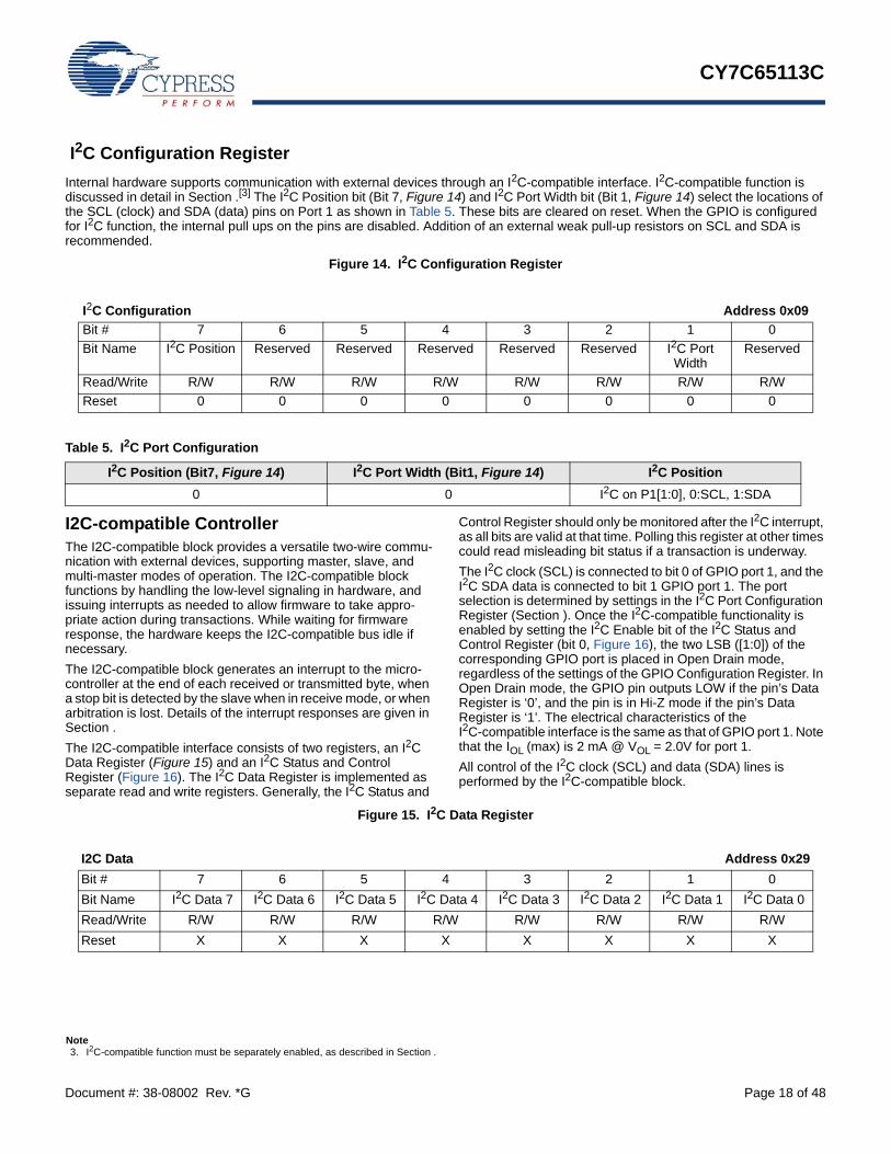
I2C Configuration RegisterInternal hardware supports communication with external devices through an I2C-compatible interface. I2C-compatible function is discussed in detail in Section .[3] The I2C Position bit (Bit 7, Figure 14) and I2C Port Width bit (Bit 1, Figure 14) select the locations of the SCL (clock) and SDA (data) pins on Port 1 as shown in Table 5. These bits are cleared on reset. When the GPIO is configured for I2C function, the internal pull ups on the pins are disabled. Addition of an external weak pull-up resistors on SCL and SDA is recommended.
Figure 14. I2C Configuration Register
.
I2C-compatible ControllerThe I2C-compatible block provides a versatile two-wire commu-nication with external devices, supporting master, slave, and multi-master modes of operation. The I2C-compatible block functions by handling the low-level signaling in hardware, and issuing interrupts as needed to allow firmware to take appro-priate action during transactions. While waiting for firmware response, the hardware keeps the I2C-compatible bus idle if necessary.The I2C-compatible block generates an interrupt to the micro-controller at the end of each received or transmitted byte, when a stop bit is detected by the slave when in receive mode, or when arbitration is lost. Details of the interrupt responses are given in Section . The I2C-compatible interface consists of two registers, an I2C Data Register (Figure 15) and an I2C Status and Control Register (Figure 16). The I2C Data Register is implemented as separate read and write registers. Generally, the I2C Status and
Control Register should only be monitored after the I2C interrupt, as all bits are valid at that time. Polling this register at other times could read misleading bit status if a transaction is underway.The I2C clock (SCL) is connected to bit 0 of GPIO port 1, and the I2C SDA data is connected to bit 1 GPIO port 1. The port selection is determined by settings in the I2C Port Configuration Register (Section ). Once the I2C-compatible functionality is enabled by setting the I2C Enable bit of the I2C Status and Control Register (bit 0, Figure 16), the two LSB ([1:0]) of the corresponding GPIO port is placed in Open Drain mode, regardless of the settings of the GPIO Configuration Register. In Open Drain mode, the GPIO pin outputs LOW if the pin’s Data Register is ‘0’, and the pin is in Hi-Z mode if the pin’s Data Register is ‘1’. The electrical characteristics of the I2C-compatible interface is the same as that of GPIO port 1. Note that the IOL (max) is 2 mA @ VOL = 2.0V for port 1.All control of the I2C clock (SCL) and data (SDA) lines is performed by the I2C-compatible block.
Figure 15. I2C Data Register
Note3. I2C-compatible function must be separately enabled, as described in Section .
I2C Configuration Address 0x09Bit # 7 6 5 4 3 2 1 0Bit Name I2C Position Reserved Reserved Reserved Reserved Reserved I2C Port
WidthReserved
Read/Write R/W R/W R/W R/W R/W R/W R/W R/WReset 0 0 0 0 0 0 0 0
Table 5. I2C Port Configuration
I2C Position (Bit7, Figure 14) I2C Port Width (Bit1, Figure 14) I2C Position0 0 I2C on P1[1:0], 0:SCL, 1:SDA
I2C Data Address 0x29Bit # 7 6 5 4 3 2 1 0Bit Name I2C Data 7 I2C Data 6 I2C Data 5 I2C Data 4 I2C Data 3 I2C Data 2 I2C Data 1 I2C Data 0Read/Write R/W R/W R/W R/W R/W R/W R/W R/WReset X X X X X X X X
CY7C65113C
Document #: 38-08002 Rev. *G Page 19 of 48
Bits [7..0]: I2C DataContains the 8-bit data on the I2C Bus
Figure 16. I2C Status and Control Register.
The I2C Status and Control register bits are defined in Table 6, with a more detailed description following.
Bit 7: MSTR ModeSetting this bit to 1 causes the I2C-compatible block to ini-tiate a master mode transaction by sending a start bit andtransmitting the first data byte from the data register (thistypically holds the target address and R/W bit). Subse-quent bytes are initiated by setting the Continue bit, asdescribed below. Clearing this bit (set to 0) causes the GPIO pins to operatenormally.In master mode, the I2C-compatible block generates theclock (SCK), and drives the data line as required depend-ing on transmit or receive state. The I2C-compatible blockperforms any required arbitration and clock synchroniza-tion. IN the event of a loss of arbitration, this MSTR bit iscleared, the ARB Lost bit is set, and an interrupt is gener-ated by the microcontroller. If the chip is the target of anexternal master that wins arbitration, then the interrupt isheld off until the transaction from the external master iscompleted.When MSTR Mode is cleared from 1 to 0 by a firmwarewrite, an I2C Stop bit is generated.
Bit 6: Continue/BusyThis bit is written by the firmware to indicate that the firm-ware is ready for the next byte transaction to begin. In oth-er words, the bit has responded to an interrupt request andhas completed the required update or read of the data reg-ister. During a read this bit indicates if the hardware is busyand is locking out additional writes to the I2C Status andControl register. This locking allows the hardware to com-plete certain operations that may require an extended pe-riod of time. Following an I2C interrupt, the I2C-compatibleblock does not return to the Busy state until firmware setsthe Continue bit. This allows the firmware to make onecontrol register write without the need to check the Busybit.
Bit 5: Xmit ModeThis bit is set by firmware to enter transmit mode and per-form a data transmit in master or slave mode. Clearing thisbit sets the part in receive mode. Firmware generally de-termines the value of this bit from the R/W bit associatedwith the I2C address packet. The Xmit Mode bit state isignored when initially writing the MSTR Mode or the Re-
I2C Status and Control Address 0x28Bit # 7 6 5 4 3 2 1 0Bit Name MSTR Mode Continue/Bu
syXmit Mode ACK Addr ARB
Lost/RestartReceived
StopI2C Enable
Read/Write R/W R/W R/W R/W R/W R/W R/W R/WReset 0 0 0 0 0 0 0 0
Table 6. I2C Status and Control Register Bit Definitions
Bit Name Description0 I2C Enable When set to ‘1’, the I2C-compatible function is enabled. When cleared, I2C GPIO pins operate
normally.1 Received Stop Reads 1 only in slave receive mode, when I2C Stop bit detected (unless firmware did not ACK the
last transaction).2 ARB Lost/Restart Reads 1 to indicate master has lost arbitration. Reads 0 otherwise.
Write to 1 in master mode to perform a restart sequence (also set Continue bit).3 Addr Reads 1 during first byte after start/restart in slave mode, or if master loses arbitration.
Reads 0 otherwise. This bit should always be written as 0.4 ACK In receive mode, write 1 to generate ACK, 0 for no ACK.
In transmit mode, reads 1 if ACK was received, 0 if no ACK received.5 Xmit Mode Write to 1 for transmit mode, 0 for receive mode.6 Continue/Busy Write 1 to indicate ready for next transaction.
Reads 1 when I2C-compatible block is busy with a transaction, 0 when transaction is complete.7 MSTR Mode Write to 1 for master mode, 0 for slave mode. This bit is cleared if master loses arbitration.
Clearing from 1 to 0 generates Stop bit.
CY7C65113C
Document #: 38-08002 Rev. *G Page 20 of 48
start bits, as these cases always cause transmit mode forthe first byte.
Bit 4: ACK This bit is set or cleared by firmware during receive oper-ation to indicate if the hardware should generate an ACKsignal on the I2C-compatible bus. Writing a 1 to this bitgenerates an ACK (SDA LOW) on the I2C-compatible busat the ACK bit time. During transmits (Xmit Mode = 1), thisbit should be cleared.
Bit 3: Addr This bit is set by the I2C-compatible block during the firstbyte of a slave receive transaction, after an I2C start orrestart. The Addr bit is cleared when the firmware sets theContinue bit. This bit allows the firmware to recognizewhen the master has lost arbitration, and in slave mode itallows the firmware to recognize that a start or restart hasoccurred.
Bit 2: ARB Lost/Restart
This bit is valid as a status bit (ARB Lost) after mastermode transactions. In master mode, set this bit (along withthe Continue and MSTR Mode bits) to perform an I2C re-start sequence. The I2C target address for the restart mustbe written to the data register before setting the Continuebit. To prevent false ARB Lost signals, the Restart bit iscleared by hardware during the restart sequence.
Bit 1: Receive StopThis bit is set when the slave is in receive mode and de-tects a stop bit on the bus. The Receive Stop bit is not setif the firmware terminates the I2C transaction by not ac-knowledging the previous byte transmitted on theI2C-compatible bus, e.g., in receive mode if firmware setsthe Continue bit and clears the ACK bit.
Bit 0: I2C EnableSet this bit to override GPIO definition with I2C-compatiblefunction on the two I2C-compatible pins. When this bit iscleared, these pins are free to function as GPIOs. InI2C-compatible mode, the two pins operate in open drainmode, independent of the GPIO configuration setting.
Processor Status and Control RegisterFigure 17. Processor Status and Control Register
Bit 0: RunThis bit is manipulated by the HALT instruction. When Haltis executed, all the bits of the Processor Status and ControlRegister are cleared to 0. Since the run bit is cleared, theprocessor stops at the end of the current instruction. Theprocessor remains halted until an appropriate reset occurs(power-on or Watchdog). This bit should normally be writ-ten as a ‘1.’
Bit 1: ReservedBit 1 is reserved and must be written as a zero.
Bit 2: Interrupt Enable SenseThis bit indicates whether interrupts are enabled or dis-abled. Firmware has no direct control over this bit as writ-ing a zero or one to this bit position has no effect on inter-rupts. A ‘0’ indicates that interrupts are masked off and a‘1’ indicates that the interrupts are enabled. This bit is fur-ther gated with the bit settings of the Global Interrupt En-able Register (Figure 18) and USB End Point Interrupt En-able Register (Figure 19). Instructions DI, EI, and RETImanipulate the state of this bit.
Bit 3: Suspend
Writing a ‘1’ to the Suspend bit halts the processor andcause the microcontroller to enter the suspend mode thatsignificantly reduces power consumption. A pending, en-abled interrupt or USB bus activity causes the device tocome out of suspend. After coming out of suspend, thedevice resumes firmware execution at the instruction fol-lowing the IOWR which put the part into suspend. AnIOWR attempting to put the part into suspend is ignored ifUSB bus activity is present. See Section for more detailson suspend mode operation.
Bit 4: Power-on ResetThe Power-on Reset is set to ‘1’ during a power-on reset.The firmware can check bits 4 and 6 in the reset handlerto determine whether a reset was caused by a power-oncondition or a Watchdog timeout. A POR event may befollowed by a Watchdog reset before firmware begins ex-ecuting, as explained below.
Bit 5: USB Bus Reset InterruptThe USB Bus Reset Interrupt bit is set when the USB BusReset is detected on receiving a USB Bus Reset signal onthe upstream port. The USB Bus Reset signal is a sin-gle-ended zero (SE0) that lasts from 12 to 16 μs. An SE0
Processor Status and Control Address 0xFFBit # 7 6 5 4 3 2 1 0Bit Name IRQ
Pending Watchdog
ResetUSB Bus
Reset Interrupt
Power-on Reset
Suspend InterruptEnable Sense
Reserved Run
Read/Write R R/W R/W R/W R/W R R/W R/WReset 0 0 0 1 0 0 0 1
CY7C65113C
Document #: 38-08002 Rev. *G Page 21 of 48
is defined as the condition in which both the D+ line andthe D– line are LOW at the same time.
Bit 6: Watchdog ResetThe Watchdog Reset is set during a reset initiated by theWatchdog Timer. This indicates the Watchdog Timer wentfor more than tWATCH (8 ms minimum) between Watchdogclears. This can occur with a POR event, as noted below.
Bit 7: IRQ PendingThe IRQ pending, when set, indicates that one or more ofthe interrupts has been recognized as active. An interruptremains pending until its interrupt enable bit is set(Figure 18, Figure 19) and interrupts are globally enabled.At that point, the internal interrupt handling sequenceclears this bit until another interrupt is detected as pending.
During power-up, the Processor Status and Control Register is set to 00010001, which indicates a POR (bit 4 set) has occurred and no interrupts are pending (bit 7 clear). During the 96-ms suspend at start-up (explained in Section ), a Watchdog Reset also occurs unless this suspend is aborted by an upstream SE0
before 8 ms. If a WDR occurs during the power-up suspend interval, firmware reads 01010001 from the Status and Control Register after power-up. Normally, the POR bit should be cleared so a subsequent WDR can be clearly identified. If an upstream bus reset is received before firmware examines this register, the Bus Reset bit may also be set.During a Watchdog Reset, the Processor Status and Control Register is set to 01XX0001, which indicates a Watchdog Reset (bit 6 set) has occurred and no interrupts are pending (bit 7 clear). The Watchdog Reset does not effect the state of the POR and the Bus Reset Interrupt bits.
InterruptsInterrupts are generated by GPIO pins, internal timers, I2C-compatible operation, internal USB hub and USB traffic conditions. All interrupts are maskable by the Global Interrupt Enable Register and the USB End Point Interrupt Enable Register. Writing a ‘1’ to a bit position enables the interrupt associated with that bit position.
Figure 18. Global Interrupt Enable Register
Bit 0: USB Bus RST Interrupt Enable1 = Enable Interrupt on a USB Bus Reset; 0 = Disableinterrupt on a USB Bus Reset (Refer to section ).
Bit 1:128-μs Interrupt Enable1 = Enable Timer interrupt every 128 μs; 0 = Disable TimerInterrupt for every 128 μs.
Bit 2: 1.024-ms Interrupt Enable1 = Enable Timer interrupt every 1.024 ms; 0 = DisableTimer Interrupt every 1.024 ms.
Bit 3: USB Hub Interrupt Enable
1 = Enable Interrupt on a Hub status change; 0 = Disableinterrupt due to hub status change. (Refer to section .)
Bit 4: Reserved.Bit 5: GPIO Interrupt Enable
1 = Enable Interrupt on falling/rising edge on any GPIO; 0= Disable Interrupt on falling/rising edge on any GPIO (Re-fer to section , and .).
Bit 6: I2C Interrupt Enable1 = Enable Interrupt on I2C related activity; 0 = Disable I2Crelated activity interrupt. (Refer to section .)
Bit 7: Reserved
Figure 19. USB Endpoint Interrupt Enable Register.
Global Interrupt Enable Register Address 0X20Bit # 7 6 5 4 3 2 1 0Bit Name Reserved I2C Interrupt
EnableGPIO
Interrupt Enable
Reserved USB Hub Interrupt Enable
1.024-ms Interrupt Enable
128-μs Interrupt Enable
USB Bus RST
Interrupt Enable
Read/Write – R/W R/W - R/W R/W R/W R/WReset – 0 0 X 0 0 0 0
USB Endpoint Interrupt Enable Address 0X21Bit # 7 6 5 4 3 2 1 0Bit Name Reserved Reserved Reserved EPB1
Interrupt Enable
EPB0 Interrupt Enable
EPA2 Interrupt Enable
EPA1 Interrupt Enable
EPA0 Interrupt Enable
Read/Write – – – R/W R/W R/W R/W R/WReset – – – 0 0 0 0 0
CY7C65113C
Document #: 38-08002 Rev. *G Page 22 of 48
Bit 0: EPA0 Interrupt Enable 1 = Enable Interrupt on data activity through endpoint A0;0 = Disable Interrupt on data activity through endpoint A0
Bit 1: EPA1 Interrupt Enable 1 = Enable Interrupt on data activity through endpoint A1;0 = Disable Interrupt on data activity through endpoint A1
Bit 2: EPA2 Interrupt Enable 1 = Enable Interrupt on data activity through endpoint A2;0 = Disable Interrupt on data activity through endpoint A2.
Bit 3: EPB0 Interrupt Enable 1 = Enable Interrupt on data activity through endpoint B0;0 = Disable Interrupt on data activity through endpoint B0
Bit 4: EPB1 Interrupt Enable 1 = Enable Interrupt on data activity through endpoint B1;0 = Disable Interrupt on data activity through endpoint B1
Bit [7..5]: Reserved During a reset, the contents of the Global Interrupt Enable Register and USB End Point Interrupt Enable Register are cleared, effectively disabling all interrupts,The interrupt controller contains a separate flip-flop for each interrupt. See Figure 20 for the logic block diagram of the interrupt controller. When an interrupt is generated, it is first registered as a pending interrupt. It stays pending until it is serviced or a reset occurs. A pending interrupt only generates an interrupt request if it is enabled by the corresponding bit in the interrupt enable registers. The highest priority interrupt request is serviced following the completion of the currently executing instruction.When servicing an interrupt, the hardware does the following:
1. Disables all interrupts by clearing the Global Interrupt Enable bit in the CPU (the state of this bit can be read at Bit 2 of the Processor Status and Control Register, Figure 17).
2. Clears the flip-flop of the current interrupt. 3. Generates an automatic CALL instruction to the ROM
address associated with the interrupt being serviced (i.e., the Interrupt Vector, see Section ).
The instruction in the interrupt table is typically a JMP instruction to the address of the Interrupt Service Routine (ISR). The user can reenable interrupts in the interrupt service routine by executing an EI instruction. Interrupts can be nested to a level limited only by the available stack space.The Program Counter value as well as the Carry and Zero flags (CF, ZF) are stored onto the Program Stack by the automatic CALL instruction generated as part of the interrupt acknowledge process. The user firmware is responsible for ensuring that the processor state is preserved and restored during an interrupt. The PUSH A instruction should typically be used as the first command in the ISR to save the accumulator value and the POP A instruction should be used to restore the accumulator value just before the RETI instruction. The program counters CF and ZF are restored and interrupts are enabled when the RETI instruction is executed.The IDI and EI instruction can be used to disable and enable interrupts, respectively. These instruction affect only the Global Interrupt Enable bit of the CPU. If desired, EI can be used to re-enable interrupts while inside an ISR, instead of waiting for the RETI that exits the ISR. While the global interrupt enable bit is cleared, the presence of a pending interrupt can be detected by examining the IRQ Sense bit (Bit 7 in the Processor Status and Control Register).
CY7C65113C
Document #: 38-08002 Rev. *G Page 23 of 48
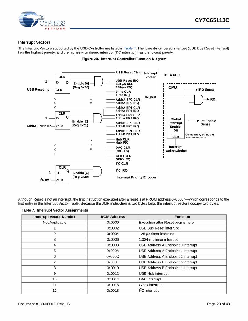
Interrupt VectorsThe Interrupt Vectors supported by the USB Controller are listed in Table 7. The lowest-numbered interrupt (USB Bus Reset interrupt) has the highest priority, and the highest-numbered interrupt (I2C interrupt) has the lowest priority.
Figure 20. Interrupt Controller Function Diagram
Although Reset is not an interrupt, the first instruction executed after a reset is at PROM address 0x0000h—which corresponds to the first entry in the Interrupt Vector Table. Because the JMP instruction is two bytes long, the interrupt vectors occupy two bytes.
Table 7. Interrupt Vector Assignments
Interrupt Vector Number ROM Address FunctionNot Applicable 0x0000 Execution after Reset begins here
1 0x0002 USB Bus Reset interrupt2 0x0004 128-μs timer interrupt3 0x0006 1.024-ms timer interrupt4 0x0008 USB Address A Endpoint 0 interrupt5 0x000A USB Address A Endpoint 1 interrupt6 0x000C USB Address A Endpoint 2 interrupt7 0x000E USB Address B Endpoint 0 interrupt8 0x0010 USB Address B Endpoint 1 interrupt9 0x0012 USB Hub interrupt
10 0x0014 DAC interrupt11 0x0016 GPIO interrupt12 0x0018 I2C interrupt
CLR
GlobalInterrupt
InterruptAcknowledge
IRQout
USB Reset Clear Interrupt
Interrupt Priority Encoder
Enable [0]D Q 1
Enable Bit
CLR
USB Reset IRQ128-μs CLR128-μs IRQ1-ms CLR1-ms IRQ
AddrA EP0 IRQAddrA EP0 CLR
I2C IRQ
Vector
Enable [6]
CLK
CLRD Q
CLK
1
I2C CLR
I2C Int
USB Reset Int
AddrA EP1 IRQAddrA EP1 CLR
IRQ Sense
IRQ
Controlled by DI, EI, and RETI Instructions
DAC IRQDAC CLR
To CPU
CPU
GPIO IRQGPIO CLR
Hub IRQHub CLR
AddrA EP2 IRQAddrA EP2 CLR
AddrB EP0 IRQAddrB EP0 CLR
AddrB EP1 IRQAddrB EP1 CLR
(Reg 0x20)
(Reg 0x20)
CLR
Enable [2]D Q 1
CLKAddrA ENP2 Int (Reg 0x21)Int EnableSense
CY7C65113C
Document #: 38-08002 Rev. *G Page 24 of 48
Interrupt LatencyInterrupt latency can be calculated from the following equation:
For example, if a 5-clock cycle instruction such as JC is being executed when an interrupt occurs, the first instruction of the Interrupt Service Routine executes a minimum of 16 clocks (1+10+5) or a maximum of 20 clocks (5+10+5) after the interrupt is issued. For a 12-MHz internal clock (6-MHz crystal), 20 clock periods is 20/12 MHz = 1.667 μs.
USB Bus Reset InterruptThe USB Controller recognizes a USB Reset when a Single Ended Zero (SE0) condition persists on the upstream USB port for 12–16 μs. SE0 is defined as the condition in which both the D+ line and the D– line are LOW. A USB Bus Reset may be recognized for an SE0 as short as 12 μs, but is always recog-nized for an SE0 longer than 16 μs. When a USB Bus Reset is detected, bit 5 of the Processor Status and Control Register (Figure 17) is set to record this event. In addition, the controller clears the following registers:SIE Section:.....USB Device Address Registers (0x10, 0x40)Hub Section: ......................Hub Ports Connect Status (0x48)........................................................ Hub Ports Enable (0x49).........................................................Hub Ports Speed (0x4A).....................................................Hub Ports Suspend (0x4D)...........................................Hub Ports Resume Status (0x4E)................................................. Hub Ports SE0 Status (0x4F)............................................................Hub Ports Data (0x50)............................................. Hub Downstream Force (0x51).A USB Bus Reset Interrupt is generated at the end of the USB Bus Reset condition when the SE0 state is deasserted. If the USB reset occurs during the start-up delay following a POR, the delay is aborted as described in Section .
Timer InterruptThere are two periodic timer interrupts: the 128-μs interrupt and the 1.024-ms interrupt. The user should disable both timer inter-rupts before going into the suspend mode to avoid possible conflicts between servicing the timer interrupts first or the suspend request first.
USB Endpoint InterruptsThere are five USB endpoint interrupts, one per endpoint. A USB endpoint interrupt is generated after the USB host writes to a USB endpoint FIFO or after the USB controller sends a packet to the USB host. The interrupt is generated on the last packet of the transaction (e.g., on the host’s ACK on an IN transfer, or on the device ACK on an OUT transfer). If no ACK is received during an IN transaction, no interrupt is generated.
USB Hub InterruptA USB hub interrupt is generated by the hardware after a connect/disconnect change, babble, or a resume event is detected by the USB repeater hardware. The babble and resume events are additionally gated by the corresponding bits of the Hub Port Enable Register (Figure 24). The connect/disconnect event on a port does not generate an interrupt if the SIE does not drive the port (i.e., the port is being forced).
GPIO InterruptEach of the GPIO pins can generate an interrupt, if enabled. The interrupt polarity can be programmed for each GPIO port as part of the GPIO configuration. All of the GPIO pins share a single interrupt vector, which means the firmware needs to read the GPIO ports with enabled interrupts to determine which pin or pins caused an interrupt. A block diagram of the GPIO interrupt logic is shown in Figure .
Interrupt latency = (Number of clock cycles remaining in the current instruction) + (10 clock cycles for the CALL instruction) + (5 clock cycles for the JMP instruction)
CY7C65113C
Document #: 38-08002 Rev. *G Page 25 of 48
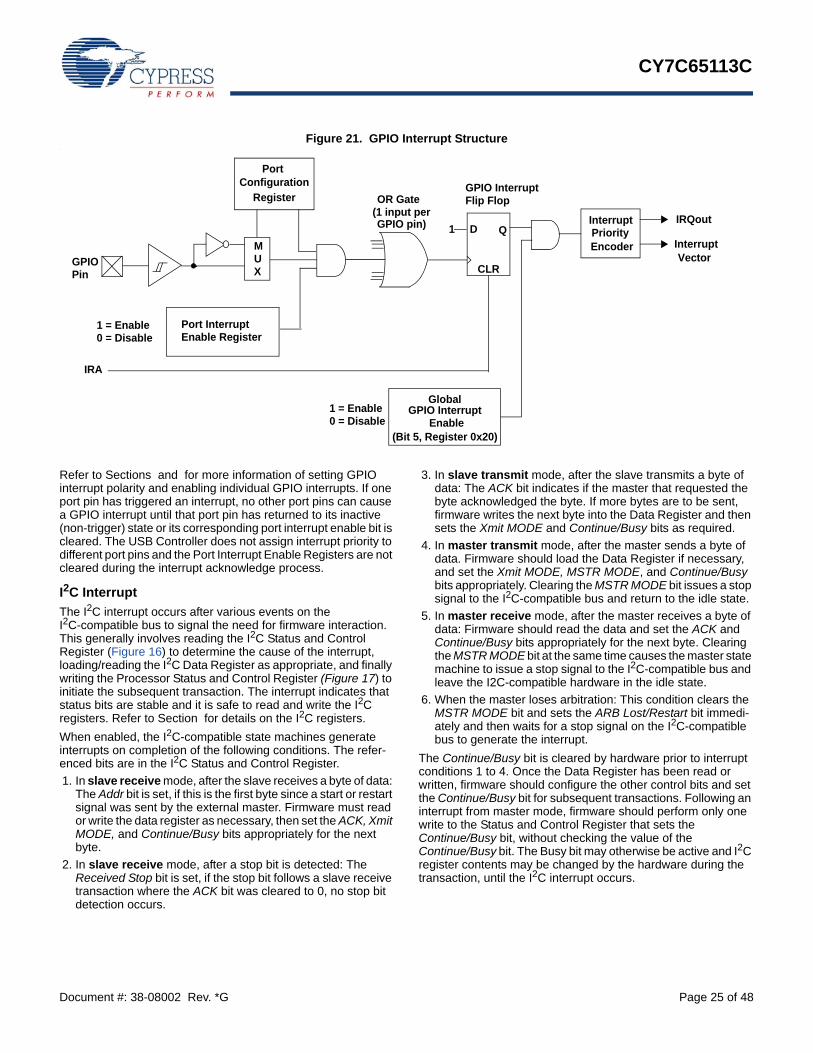
Figure 21. GPIO Interrupt Structure.
Refer to Sections and for more information of setting GPIO interrupt polarity and enabling individual GPIO interrupts. If one port pin has triggered an interrupt, no other port pins can cause a GPIO interrupt until that port pin has returned to its inactive (non-trigger) state or its corresponding port interrupt enable bit is cleared. The USB Controller does not assign interrupt priority to different port pins and the Port Interrupt Enable Registers are not cleared during the interrupt acknowledge process.
I2C InterruptThe I2C interrupt occurs after various events on the I2C-compatible bus to signal the need for firmware interaction. This generally involves reading the I2C Status and Control Register (Figure 16) to determine the cause of the interrupt, loading/reading the I2C Data Register as appropriate, and finally writing the Processor Status and Control Register (Figure 17) to initiate the subsequent transaction. The interrupt indicates that status bits are stable and it is safe to read and write the I2C registers. Refer to Section for details on the I2C registers.When enabled, the I2C-compatible state machines generate interrupts on completion of the following conditions. The refer-enced bits are in the I2C Status and Control Register.1. In slave receive mode, after the slave receives a byte of data:
The Addr bit is set, if this is the first byte since a start or restart signal was sent by the external master. Firmware must read or write the data register as necessary, then set the ACK, Xmit MODE, and Continue/Busy bits appropriately for the next byte.
2. In slave receive mode, after a stop bit is detected: The Received Stop bit is set, if the stop bit follows a slave receive transaction where the ACK bit was cleared to 0, no stop bit detection occurs.
3. In slave transmit mode, after the slave transmits a byte of data: The ACK bit indicates if the master that requested the byte acknowledged the byte. If more bytes are to be sent, firmware writes the next byte into the Data Register and then sets the Xmit MODE and Continue/Busy bits as required.
4. In master transmit mode, after the master sends a byte of data. Firmware should load the Data Register if necessary, and set the Xmit MODE, MSTR MODE, and Continue/Busy bits appropriately. Clearing the MSTR MODE bit issues a stop signal to the I2C-compatible bus and return to the idle state.
5. In master receive mode, after the master receives a byte of data: Firmware should read the data and set the ACK and Continue/Busy bits appropriately for the next byte. Clearing the MSTR MODE bit at the same time causes the master state machine to issue a stop signal to the I2C-compatible bus and leave the I2C-compatible hardware in the idle state.
6. When the master loses arbitration: This condition clears the MSTR MODE bit and sets the ARB Lost/Restart bit immedi-ately and then waits for a stop signal on the I2C-compatible bus to generate the interrupt.
The Continue/Busy bit is cleared by hardware prior to interrupt conditions 1 to 4. Once the Data Register has been read or written, firmware should configure the other control bits and set the Continue/Busy bit for subsequent transactions. Following an interrupt from master mode, firmware should perform only one write to the Status and Control Register that sets the Continue/Busy bit, without checking the value of the Continue/Busy bit. The Busy bit may otherwise be active and I2C register contents may be changed by the hardware during the transaction, until the I2C interrupt occurs.
Port
Register OR GateGPIO InterruptFlip Flop
CLRGPIOPin
1 = Enable0 = Disable
Port InterruptEnable Register
1 = Enable0 = Disable
InterruptPriorityEncoder
IRQout
Interrupt Vector
D QMUX
1(1 input per GPIO pin)
GlobalGPIO Interrupt
Enable(Bit 5, Register 0x20)
IRA
Configuration
CY7C65113C
Document #: 38-08002 Rev. *G Page 26 of 48
USB OverviewThe USB hardware includes a USB Hub repeater with one upstream and up to seven downstream ports. The USB Hub repeater interfaces to the microcontroller through a full-speed serial interface engine (SIE). An external series resistor of Rext must be placed in series with all upstream and downstream USB outputs in order to meet the USB driver requirements of the USB specification. The CY7C65113C microcontroller can provide the functionality of a compound device consisting of a USB hub and permanently attached functions.
USB Serial Interface Engine (SIE)The SIE allows the CY7C65113C microcontroller to commu-nicate with the USB host through the USB repeater portion of the hub. The SIE simplifies the interface between the microcontroller and USB by incorporating hardware that handles the following USB bus activity independently of the microcontroller:• Bit stuffing/unstuffing• Checksum generation/checking• ACK/NAK/STALL• Token type identification• Address checking.
Firmware is required to handle the following USB interface tasks:• Coordinate enumeration by responding to SETUP packets• Fill and empty the FIFOs• Suspend/Resume coordination• Verify and select DATA toggle values.
USB EnumerationThe internal hub and any compound device function are enumerated under firmware control. The hub is enumerated first, followed by any integrated compound function. After the hub is enumerated, the USB host can read hub connection status to determine which (if any) of the downstream ports need to be enumerated. The following is a brief summary of the typical enumeration process of the CY7C65113C by the USB host. For a detailed description of the enumeration process, refer to the USB specification. In this description, ‘Firmware’ refers to embedded firmware in the CY7C65113C controller.1. The host computer sends a SETUP packet followed by a
DATA packet to USB address 0 requesting the Device de-scriptor.
2. Firmware decodes the request and retrieves its Device descriptor from the program memory tables.
3. The host computer performs a control read sequence and Firmware responds by sending the Device descriptor over the USB bus, via the on-chip FIFOs.
4. After receiving the descriptor, the host sends a SETUP packet followed by a DATA packet to address 0 assigning a new USB address to the device.
5. Firmware stores the new address in its USB Device Address Register (for example, as Address B) after the no-data control sequence completes.
6. The host sends a request for the Device descriptor using the new USB address.
7. Firmware decodes the request and retrieves the Device descriptor from program memory tables.
8. The host performs a control read sequence and Firmware responds by sending its Device descriptor over the USB bus.
9. The host generates control reads from the device to request the Configuration and Report descriptors.
10.Once the device receives a Set Configuration request, its functions may now be used.
11.Following enumeration as a hub, Firmware can optionally indicate to the host that a compound device exists (for example, the keyboard in a keyboard/hub device).
12.The host carries out the enumeration process with this additional function as though it were attached downstream from the hub.
13.When the host assigns an address to this device, it is stored as the other USB address (for example, Address A).
USB HubA USB hub is required to support:• Connectivity behavior: service connect/disconnect detection• Bus fault detection and recovery• Full-/Low-speed device support
These features are mapped onto a hub repeater and a hub controller. The hub controller is supported by the processor integrated into the CY7C65113C microcontroller. The hardware in the hub repeater detects whether a USB device is connected to a downstream port. The connection to a downstream port is through a differential signal pair (D+ and D–). Each downstream port provided by the hub requires external RUDN resistors from each signal line to ground, so that when a downstream port has no device connected, the hub reads a LOW (zero) on both D+ and D–. This condition is used to identify the “no connect” state.The hub must have a resistor RUUP connected between its upstream D+ line and VREG to indicate it is a full speed USB device.The hub generates an EOP at EOF1, in accordance with the USB 1.1 Specification (section 11.2.2, page 234) as well as USB 2.0 specification (section 11.2.5, page 304).
Connecting/Disconnecting a USB DeviceA low-speed (1.5 Mbps) USB device has a pull-up resistor on the D– pin. At connect time, the bias resistors set the signal levels on the D+ and D– lines. When a low-speed device is connected to a hub port, the hub sees a LOW on D+ and a HIGH on D–. This causes the hub repeater to set a connect bit in the Hub Ports Connect Status register for the downstream port (see Figure 22). Then the hub repeater generates a Hub Interrupt to notify the microcontroller that there has been a change in the Hub downstream status. The firmware sets the speed of this port in the Hub Ports Speed Register (see Figure ).A full-speed (12 Mbps) USB device has a pull-up resistor from the D+ pin, so the hub sees a HIGH on D+ and a LOW on D–. In this case, the hub repeater sets a connect bit in the Hub Ports Connect Status register and generates a Hub Interrupt to notify the microcontroller of the change in Hub status. The firmware sets the speed of this port in the Hub Ports Speed Register (see Figure )

CY7C65113C
Document #: 38-08002 Rev. *G Page 27 of 48
Connects are recorded by the time a non-SE0 state lasts for more than 2.5 μs on a downstream port.When a USB device is disconnected from the Hub, the downstream signal pair eventually floats to a single-ended zero
state. The hub repeater recognizes a disconnect once the SE0 state on a downstream port lasts from 2.0 to 2.5 μs. On a disconnect, the corresponding bit in the Hub Ports Connect Status register is cleared, and the Hub Interrupt is generated.
Figure 22. Hub Ports Connect Status
.
Bit [0..3]: Port x Connect Status (where x = 1..4).When set to 1, Port x is connected; When set to 0, Port xis disconnected.
Bit [4..7]: Reserved.
Set to 0.The Hub Ports Connect Status register is cleared to zero by reset or USB bus reset, then set to match the hardware configuration by the hub repeater hardware. The Reserved bits [4..7] should always read as ‘0’ to indicate no connection.
Figure 23. Hub Ports Speed
Bit [0..3]: Port x Speed (where x = 1..4).Set to 1 if the device plugged in to Port x is Low Speed; Setto 0 if the device plugged in to Port x is Full Speed.
Bit [4..7]: Reserved. Set to 0.
The Hub Ports Speed register is cleared to zero by reset or bus reset. This must be set by the firmware on issuing a port reset. The Reserved bits [4..7] should always read as ‘0.’
Enabling/Disabling a USB DeviceAfter a USB device connection has been detected, firmware must update status change bits in the hub status change data structure that is polled periodically by the USB host. The host responds by sending a packet that instructs the hub to reset and enable the downstream port. Firmware then sets the bit in the Hub Ports Enable register (Figure 24), for the downstream port. The hub repeater hardware responds to an enable bit in the Hub
Ports Enable register (Figure 24) by enabling the downstream port, so that USB traffic can flow to and from that port.If a port is marked enabled and is not suspended, it receives all USB traffic from the upstream port, and USB traffic from the downstream port is passed to the upstream port (unless babble is detected). Low-speed ports do not receive full-speed traffic from the upstream port. When firmware writes to the Hub Ports Enable register (Figure 24) to enable a port, the port is not enabled until the end of any packet currently being transmitted. If there is no USB traffic, the port is enabled immediately.When a USB device disconnection has been detected, firmware must update status bits in the hub change status data structure that is polled periodically by the USB host. In suspended mode, a connect or disconnect event generates an interrupt (if the hub interrupt is enabled) even if the port is disabled.
Figure 24. Hub Ports Enable Register
Hub Ports Connect Status Address 0x48Bit # 7 6 5 4 3 2 1 0Bit Name Reserved Reserved Reserved Reserved Port 4
Connect Status
Port 3 Connect Status
Port 2 Connect Status
Port 1 Connect Status
Read/Write R/W R/W R/W R/W R/W R/W R/W R/WReset 0 0 0 0 0 0 0 0
Hub Ports Speed Address 0x4ABit # 7 6 5 4 3 2 1 0Bit Name Reserved Reserved Reserved Reserved Port 4 Speed Port 3 Speed Port 2 Speed Port 1 SpeedRead/Write R/W R/W R/W R/W R/W R/W R/W R/WReset 0 0 0 0 0 0 0 0
Hub Ports Enable Register Address 0x49Bit # 7 6 5 4 3 2 1 0Bit Name Reserved Reserved Reserved Reserved Port 4 Enable Port 3 Enable Port 2 Enable Port 1 EnableRead/Write R/W R/W R/W R/W R/W R/W R/W R/WReset 0 0 0 0 0 0 0 0

CY7C65113C
Document #: 38-08002 Rev. *G Page 28 of 48
Bit [0..3]: Port x Enable (where x = 1..4)Set to 1 if Port x is enabled; Set to 0 if Port x is disabled
Bit [4..7]: Reserved. Set to 0.
The Hub Ports Enable register is cleared to zero by reset or bus reset to disable all downstream ports as the default condition. A port is also disabled by internal hub hardware (enable bit cleared) if babble is detected on that downstream port. Babble is defined as:• Any non-idle downstream traffic on an enabled downstream
port at EOF2.• Any downstream port with upstream connectivity established
at EOF2 (i.e., no EOP received by EOF2).
Hub Downstream Ports Status and ControlData transfer on hub downstream ports is controlled according to the bit settings of the Hub Downstream Ports Control Register (Figure 25). Each downstream port is controlled by two bits, as
defined in Table 8 below. The Hub Downstream Ports Control Register is cleared upon reset or bus reset, and the reset state is the state for normal USB traffic. Any downstream port being forced must be marked as disabled (Figure 24) for proper operation of the hub repeater.Firmware should use this register for driving bus reset and resume signaling to downstream ports. Controlling the port pins through this register uses standard USB edge rate control according to the speed of the port, set in the Hub Port Speed Register.The downstream USB ports are designed for connection of USB devices, but can also serve as output ports under firmware control. This allows unused USB ports to be used for functions such as driving LEDs or providing additional input signals. Pulling up these pins to voltages above VREF may cause current flow into the pin. This register is not reset by USB bus reset. These bits must be cleared before going into suspend.
Figure 25. Hub Downstream Ports Control Register
An alternate means of forcing the downstream ports is through the Hub Ports Force Low Register (Figure 26) Register. With this register the pins of the downstream ports can be individually forced LOW, or left unforced. Unlike the Hub Downstream Ports Control Register, above, the Force Low Register does not produce standard USB edge rate control on the forced pins. However, this register allows downstream port pins to be held LOW in suspend. This register can be used to drive SE0 on all downstream ports when unconfigured, as required in the USB 1.1 specification.
Figure 26. Hub Ports Force Low Register
.
Hub Downstream Ports Control Register Address 0x4BBit # 7 6 5 4 3 2 1 0Bit Name Port 4
Control Bit 1Port 4
Control Bit 0Port 3
Control Bit 1Port 3
Control Bit 0Port 2
Control Bit 1Port 2
Control Bit 0Port 1
Control Bit 1Port 1
Control Bit 0Read/Write R/W R/W R/W R/W R/W R/W R/W R/WReset 0 0 0 0 0 0 0 0
Table 8. Control Bit Definition for Downstream Ports
Control BitsControl Action
Bit1 Bit 00 0 Not Forcing (Normal USB Function)0 1 Force Differential ‘1’ (D+ HIGH, D– LOW)1 0 Force Differential ‘0’ (D+ LOW, D– HIGH)1 1 Force SE0 state
Hub Ports Force Low Address 0x51Bit # 7 6 5 4 3 2 1 0Bit Name Force Low
D+[4]Force Low
D–[4]Force Low
D+[3]Force Low
D–[3]Force Low
D+[2]Force Low
D–[2]Force Low
D+[1]Force Low
D–[1]Read/Write R/W R/W R/W R/W R/W R/W R/W R/WReset 0 0 0 0 0 0 0 0
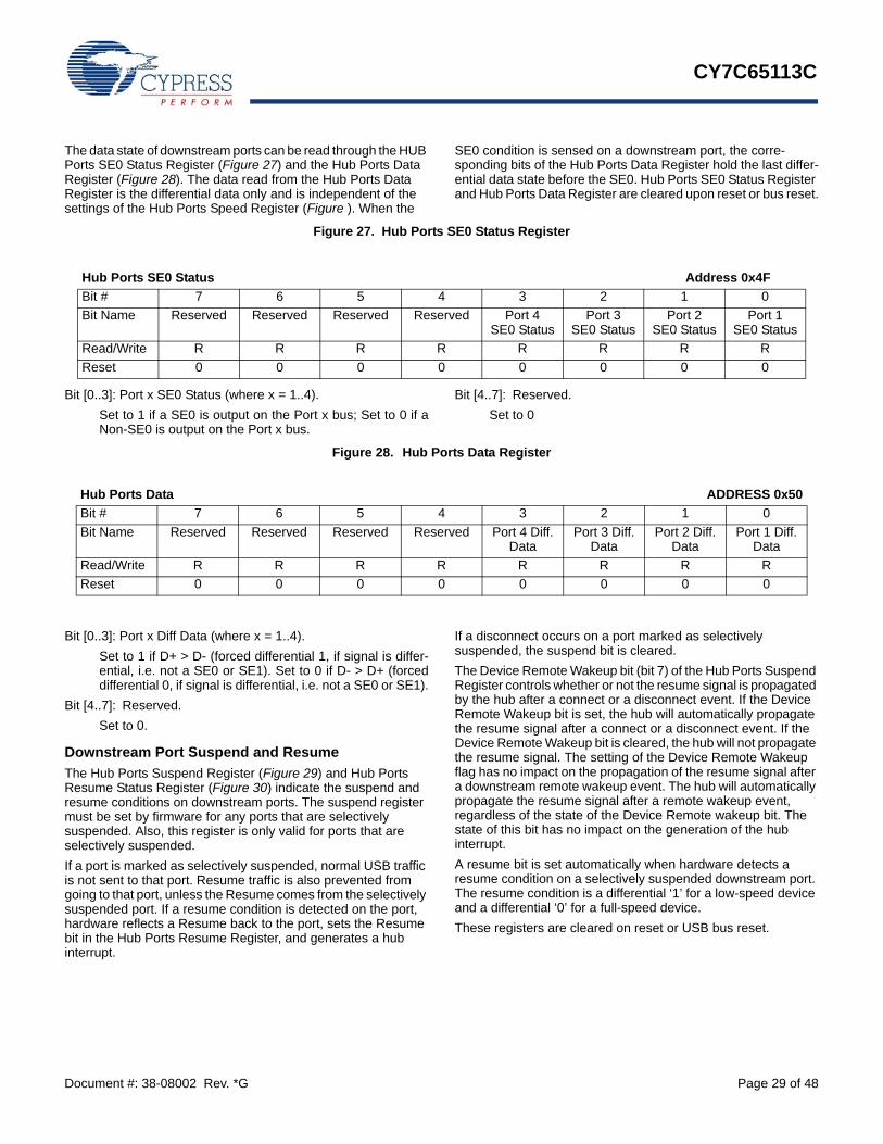
CY7C65113C
Document #: 38-08002 Rev. *G Page 29 of 48
The data state of downstream ports can be read through the HUB Ports SE0 Status Register (Figure 27) and the Hub Ports Data Register (Figure 28). The data read from the Hub Ports Data Register is the differential data only and is independent of the settings of the Hub Ports Speed Register (Figure ). When the
SE0 condition is sensed on a downstream port, the corre-sponding bits of the Hub Ports Data Register hold the last differ-ential data state before the SE0. Hub Ports SE0 Status Register and Hub Ports Data Register are cleared upon reset or bus reset.
Figure 27. Hub Ports SE0 Status Register
.
Bit [0..3]: Port x SE0 Status (where x = 1..4).Set to 1 if a SE0 is output on the Port x bus; Set to 0 if aNon-SE0 is output on the Port x bus.
Bit [4..7]: Reserved. Set to 0
Figure 28. . Hub Ports Data Register
Bit [0..3]: Port x Diff Data (where x = 1..4).Set to 1 if D+ > D- (forced differential 1, if signal is differ-ential, i.e. not a SE0 or SE1). Set to 0 if D- > D+ (forceddifferential 0, if signal is differential, i.e. not a SE0 or SE1).
Bit [4..7]: Reserved. Set to 0.
Downstream Port Suspend and ResumeThe Hub Ports Suspend Register (Figure 29) and Hub Ports Resume Status Register (Figure 30) indicate the suspend and resume conditions on downstream ports. The suspend register must be set by firmware for any ports that are selectively suspended. Also, this register is only valid for ports that are selectively suspended.If a port is marked as selectively suspended, normal USB traffic is not sent to that port. Resume traffic is also prevented from going to that port, unless the Resume comes from the selectively suspended port. If a resume condition is detected on the port, hardware reflects a Resume back to the port, sets the Resume bit in the Hub Ports Resume Register, and generates a hub interrupt.
If a disconnect occurs on a port marked as selectively suspended, the suspend bit is cleared. The Device Remote Wakeup bit (bit 7) of the Hub Ports Suspend Register controls whether or not the resume signal is propagated by the hub after a connect or a disconnect event. If the Device Remote Wakeup bit is set, the hub will automatically propagate the resume signal after a connect or a disconnect event. If the Device Remote Wakeup bit is cleared, the hub will not propagate the resume signal. The setting of the Device Remote Wakeup flag has no impact on the propagation of the resume signal after a downstream remote wakeup event. The hub will automatically propagate the resume signal after a remote wakeup event, regardless of the state of the Device Remote wakeup bit. The state of this bit has no impact on the generation of the hub interrupt.A resume bit is set automatically when hardware detects a resume condition on a selectively suspended downstream port. The resume condition is a differential ‘1’ for a low-speed device and a differential ‘0’ for a full-speed device.These registers are cleared on reset or USB bus reset.
Hub Ports SE0 Status Address 0x4FBit # 7 6 5 4 3 2 1 0Bit Name Reserved Reserved Reserved Reserved Port 4
SE0 StatusPort 3
SE0 StatusPort 2
SE0 StatusPort 1
SE0 StatusRead/Write R R R R R R R RReset 0 0 0 0 0 0 0 0
Hub Ports Data ADDRESS 0x50Bit # 7 6 5 4 3 2 1 0Bit Name Reserved Reserved Reserved Reserved Port 4 Diff.
DataPort 3 Diff.
DataPort 2 Diff.
DataPort 1 Diff.
DataRead/Write R R R R R R R RReset 0 0 0 0 0 0 0 0
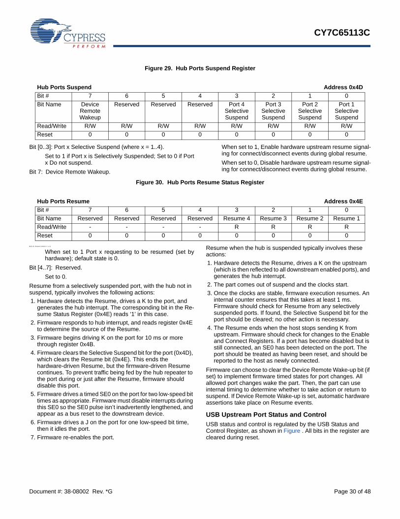
CY7C65113C
Document #: 38-08002 Rev. *G Page 30 of 48
Figure 29. Hub Ports Suspend Register
Bit [0..3]: Port x Selective Suspend (where x = 1..4).Set to 1 if Port x is Selectively Suspended; Set to 0 if Portx Do not suspend.
Bit 7: Device Remote Wakeup.
When set to 1, Enable hardware upstream resume signal-ing for connect/disconnect events during global resume.When set to 0, Disable hardware upstream resume signal-ing for connect/disconnect events during global resume.
Figure 30. Hub Ports Resume Status Register
Bit [0..3] : Resume x (where x = 1..4).
When set to 1 Port x requesting to be resumed (set byhardware); default state is 0.
Bit [4..7]: Reserved.Set to 0.
Resume from a selectively suspended port, with the hub not in suspend, typically involves the following actions:1. Hardware detects the Resume, drives a K to the port, and
generates the hub interrupt. The corresponding bit in the Re-sume Status Register (0x4E) reads ‘1’ in this case.
2. Firmware responds to hub interrupt, and reads register 0x4E to determine the source of the Resume.
3. Firmware begins driving K on the port for 10 ms or more through register 0x4B.
4. Firmware clears the Selective Suspend bit for the port (0x4D), which clears the Resume bit (0x4E). This ends the hardware-driven Resume, but the firmware-driven Resume continues. To prevent traffic being fed by the hub repeater to the port during or just after the Resume, firmware should disable this port.
5. Firmware drives a timed SE0 on the port for two low-speed bit times as appropriate. Firmware must disable interrupts during this SE0 so the SE0 pulse isn’t inadvertently lengthened, and appear as a bus reset to the downstream device.
6. Firmware drives a J on the port for one low-speed bit time, then it idles the port.
7. Firmware re-enables the port.
Resume when the hub is suspended typically involves these actions:1. Hardware detects the Resume, drives a K on the upstream
(which is then reflected to all downstream enabled ports), and generates the hub interrupt.
2. The part comes out of suspend and the clocks start. 3. Once the clocks are stable, firmware execution resumes. An
internal counter ensures that this takes at least 1 ms. Firmware should check for Resume from any selectively suspended ports. If found, the Selective Suspend bit for the port should be cleared; no other action is necessary.
4. The Resume ends when the host stops sending K from upstream. Firmware should check for changes to the Enable and Connect Registers. If a port has become disabled but is still connected, an SE0 has been detected on the port. The port should be treated as having been reset, and should be reported to the host as newly connected.
Firmware can choose to clear the Device Remote Wake-up bit (if set) to implement firmware timed states for port changes. All allowed port changes wake the part. Then, the part can use internal timing to determine whether to take action or return to suspend. If Device Remote Wake-up is set, automatic hardware assertions take place on Resume events.
USB Upstream Port Status and ControlUSB status and control is regulated by the USB Status and Control Register, as shown in Figure . All bits in the register are cleared during reset.
Hub Ports Suspend Address 0x4DBit # 7 6 5 4 3 2 1 0Bit Name Device
Remote Wakeup
Reserved Reserved Reserved Port 4 Selective Suspend
Port 3 Selective Suspend
Port 2 SelectiveSuspend
Port 1 Selective Suspend
Read/Write R/W R/W R/W R/W R/W R/W R/W R/WReset 0 0 0 0 0 0 0 0
Hub Ports Resume Address 0x4EBit # 7 6 5 4 3 2 1 0Bit Name Reserved Reserved Reserved Reserved Resume 4 Resume 3 Resume 2 Resume 1Read/Write - - - - R R R RReset 0 0 0 0 0 0 0 0
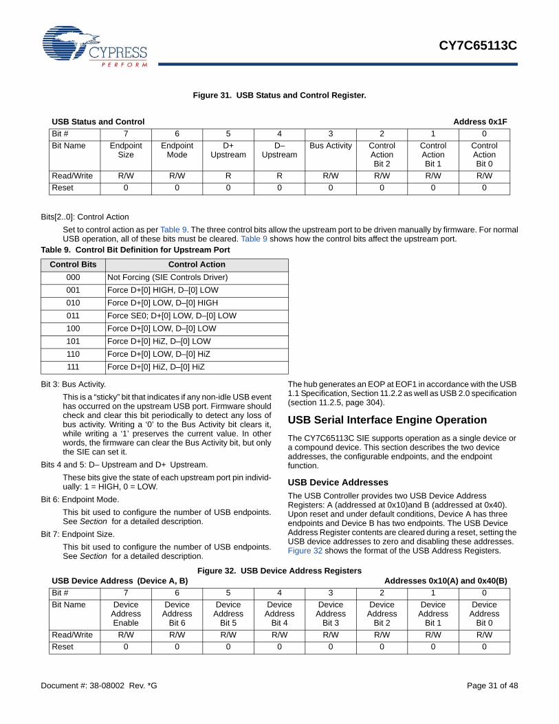
CY7C65113C
Document #: 38-08002 Rev. *G Page 31 of 48
Figure 31. USB Status and Control Register.
Bits[2..0]: Control ActionSet to control action as per Table 9. The three control bits allow the upstream port to be driven manually by firmware. For normalUSB operation, all of these bits must be cleared. Table 9 shows how the control bits affect the upstream port.
Bit 3: Bus Activity.This is a “sticky” bit that indicates if any non-idle USB eventhas occurred on the upstream USB port. Firmware shouldcheck and clear this bit periodically to detect any loss ofbus activity. Writing a ‘0’ to the Bus Activity bit clears it,while writing a ‘1’ preserves the current value. In otherwords, the firmware can clear the Bus Activity bit, but onlythe SIE can set it.
Bits 4 and 5: D– Upstream and D+ Upstream.These bits give the state of each upstream port pin individ-ually: 1 = HIGH, 0 = LOW.
Bit 6: Endpoint Mode.This bit used to configure the number of USB endpoints.See Section for a detailed description.
Bit 7: Endpoint Size.This bit used to configure the number of USB endpoints.See Section for a detailed description.
The hub generates an EOP at EOF1 in accordance with the USB 1.1 Specification, Section 11.2.2 as well as USB 2.0 specification (section 11.2.5, page 304).
USB Serial Interface Engine OperationThe CY7C65113C SIE supports operation as a single device or a compound device. This section describes the two device addresses, the configurable endpoints, and the endpoint function.
USB Device AddressesThe USB Controller provides two USB Device Address Registers: A (addressed at 0x10)and B (addressed at 0x40). Upon reset and under default conditions, Device A has three endpoints and Device B has two endpoints. The USB Device Address Register contents are cleared during a reset, setting the USB device addresses to zero and disabling these addresses. Figure 32 shows the format of the USB Address Registers.
Figure 32. USB Device Address Registers
USB Status and Control Address 0x1FBit # 7 6 5 4 3 2 1 0Bit Name Endpoint
SizeEndpoint
ModeD+
UpstreamD–
UpstreamBus Activity Control
ActionBit 2
Control ActionBit 1
Control ActionBit 0
Read/Write R/W R/W R R R/W R/W R/W R/WReset 0 0 0 0 0 0 0 0
Table 9. Control Bit Definition for Upstream Port
Control Bits Control Action000 Not Forcing (SIE Controls Driver)001 Force D+[0] HIGH, D–[0] LOW010 Force D+[0] LOW, D–[0] HIGH011 Force SE0; D+[0] LOW, D–[0] LOW100 Force D+[0] LOW, D–[0] LOW101 Force D+[0] HiZ, D–[0] LOW110 Force D+[0] LOW, D–[0] HiZ111 Force D+[0] HiZ, D–[0] HiZ
USB Device Address (Device A, B) Addresses 0x10(A) and 0x40(B)Bit # 7 6 5 4 3 2 1 0Bit Name Device
Address Enable
Device Address
Bit 6
Device Address
Bit 5
Device Address
Bit 4
Device Address
Bit 3
Device Address
Bit 2
Device Address
Bit 1
Device Address
Bit 0Read/Write R/W R/W R/W R/W R/W R/W R/W R/WReset 0 0 0 0 0 0 0 0
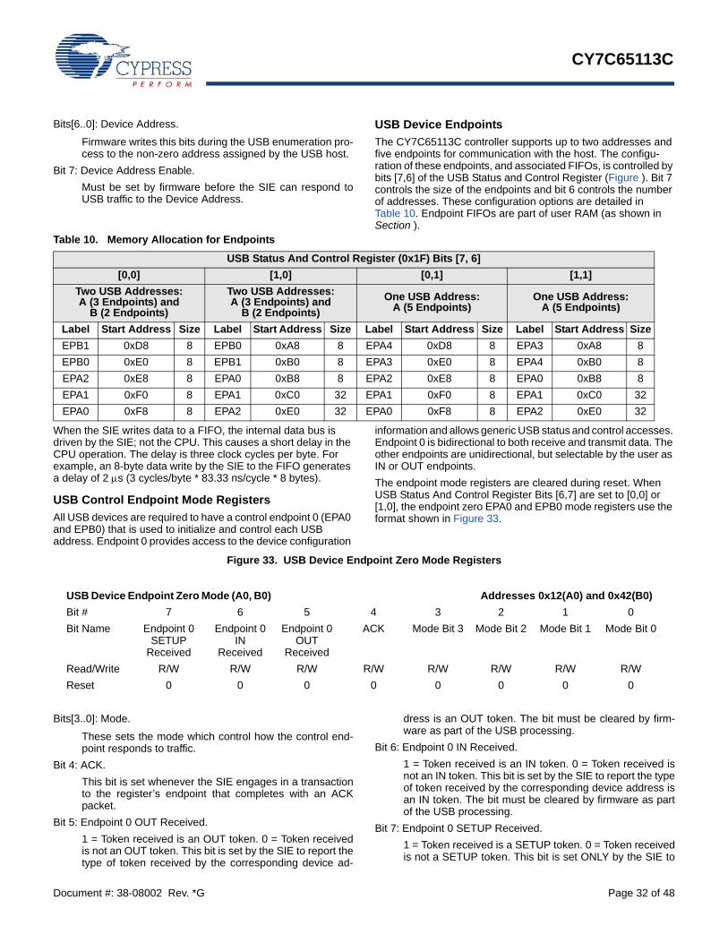
CY7C65113C
Document #: 38-08002 Rev. *G Page 32 of 48
Bits[6..0]: Device Address.
Firmware writes this bits during the USB enumeration pro-cess to the non-zero address assigned by the USB host.
Bit 7: Device Address Enable.Must be set by firmware before the SIE can respond toUSB traffic to the Device Address.
USB Device Endpoints The CY7C65113C controller supports up to two addresses and five endpoints for communication with the host. The configu-ration of these endpoints, and associated FIFOs, is controlled by bits [7,6] of the USB Status and Control Register (Figure ). Bit 7 controls the size of the endpoints and bit 6 controls the number of addresses. These configuration options are detailed in Table 10. Endpoint FIFOs are part of user RAM (as shown in Section ).
When the SIE writes data to a FIFO, the internal data bus is driven by the SIE; not the CPU. This causes a short delay in the CPU operation. The delay is three clock cycles per byte. For example, an 8-byte data write by the SIE to the FIFO generates a delay of 2 μs (3 cycles/byte * 83.33 ns/cycle * 8 bytes).
USB Control Endpoint Mode RegistersAll USB devices are required to have a control endpoint 0 (EPA0 and EPB0) that is used to initialize and control each USB address. Endpoint 0 provides access to the device configuration
information and allows generic USB status and control accesses. Endpoint 0 is bidirectional to both receive and transmit data. The other endpoints are unidirectional, but selectable by the user as IN or OUT endpoints.The endpoint mode registers are cleared during reset. When USB Status And Control Register Bits [6,7] are set to [0,0] or [1,0], the endpoint zero EPA0 and EPB0 mode registers use the format shown in Figure 33.
Figure 33. USB Device Endpoint Zero Mode Registers
Bits[3..0]: Mode.
These sets the mode which control how the control end-point responds to traffic.
Bit 4: ACK.This bit is set whenever the SIE engages in a transactionto the register’s endpoint that completes with an ACKpacket.
Bit 5: Endpoint 0 OUT Received.1 = Token received is an OUT token. 0 = Token receivedis not an OUT token. This bit is set by the SIE to report thetype of token received by the corresponding device ad-
dress is an OUT token. The bit must be cleared by firm-ware as part of the USB processing.
Bit 6: Endpoint 0 IN Received.1 = Token received is an IN token. 0 = Token received isnot an IN token. This bit is set by the SIE to report the typeof token received by the corresponding device address isan IN token. The bit must be cleared by firmware as partof the USB processing.
Bit 7: Endpoint 0 SETUP Received.1 = Token received is a SETUP token. 0 = Token receivedis not a SETUP token. This bit is set ONLY by the SIE to
Table 10. Memory Allocation for Endpoints
USB Status And Control Register (0x1F) Bits [7, 6][0,0] [1,0] [0,1] [1,1]
Two USB Addresses:A (3 Endpoints) and
B (2 Endpoints)
Two USB Addresses: A (3 Endpoints) and
B (2 Endpoints) One USB Address:
A (5 Endpoints)One USB Address:
A (5 Endpoints)
Label Start Address Size Label Start Address Size Label Start Address Size Label Start Address SizeEPB1 0xD8 8 EPB0 0xA8 8 EPA4 0xD8 8 EPA3 0xA8 8EPB0 0xE0 8 EPB1 0xB0 8 EPA3 0xE0 8 EPA4 0xB0 8EPA2 0xE8 8 EPA0 0xB8 8 EPA2 0xE8 8 EPA0 0xB8 8EPA1 0xF0 8 EPA1 0xC0 32 EPA1 0xF0 8 EPA1 0xC0 32EPA0 0xF8 8 EPA2 0xE0 32 EPA0 0xF8 8 EPA2 0xE0 32
USB Device Endpoint Zero Mode (A0, B0) Addresses 0x12(A0) and 0x42(B0)Bit # 7 6 5 4 3 2 1 0Bit Name Endpoint 0
SETUP Received
Endpoint 0 IN
Received
Endpoint 0 OUT
Received
ACK Mode Bit 3 Mode Bit 2 Mode Bit 1 Mode Bit 0
Read/Write R/W R/W R/W R/W R/W R/W R/W R/WReset 0 0 0 0 0 0 0 0
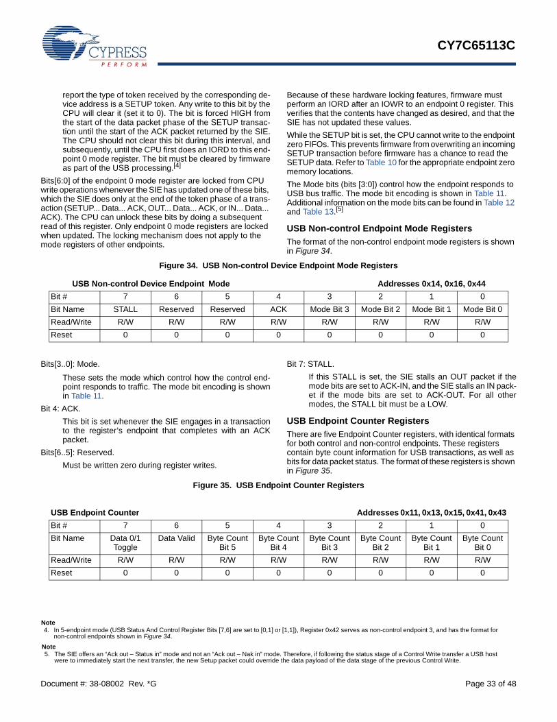
CY7C65113C
Document #: 38-08002 Rev. *G Page 33 of 48
report the type of token received by the corresponding de-vice address is a SETUP token. Any write to this bit by theCPU will clear it (set it to 0). The bit is forced HIGH fromthe start of the data packet phase of the SETUP transac-tion until the start of the ACK packet returned by the SIE.The CPU should not clear this bit during this interval, andsubsequently, until the CPU first does an IORD to this end-point 0 mode register. The bit must be cleared by firmwareas part of the USB processing.[4]
Bits[6:0] of the endpoint 0 mode register are locked from CPU write operations whenever the SIE has updated one of these bits, which the SIE does only at the end of the token phase of a trans-action (SETUP... Data... ACK, OUT... Data... ACK, or IN... Data... ACK). The CPU can unlock these bits by doing a subsequent read of this register. Only endpoint 0 mode registers are locked when updated. The locking mechanism does not apply to the mode registers of other endpoints.
Because of these hardware locking features, firmware must perform an IORD after an IOWR to an endpoint 0 register. This verifies that the contents have changed as desired, and that the SIE has not updated these values.While the SETUP bit is set, the CPU cannot write to the endpoint zero FIFOs. This prevents firmware from overwriting an incoming SETUP transaction before firmware has a chance to read the SETUP data. Refer to Table 10 for the appropriate endpoint zero memory locations.The Mode bits (bits [3:0]) control how the endpoint responds to USB bus traffic. The mode bit encoding is shown in Table 11. Additional information on the mode bits can be found in Table 12 and Table 13.[5]
USB Non-control Endpoint Mode RegistersThe format of the non-control endpoint mode registers is shown in Figure 34.
Figure 34. USB Non-control Device Endpoint Mode Registers
Bits[3..0]: Mode.
These sets the mode which control how the control end-point responds to traffic. The mode bit encoding is shownin Table 11.
Bit 4: ACK.This bit is set whenever the SIE engages in a transactionto the register’s endpoint that completes with an ACKpacket.
Bits[6..5]: Reserved.Must be written zero during register writes.
Bit 7: STALL.If this STALL is set, the SIE stalls an OUT packet if themode bits are set to ACK-IN, and the SIE stalls an IN pack-et if the mode bits are set to ACK-OUT. For all othermodes, the STALL bit must be a LOW.
USB Endpoint Counter RegistersThere are five Endpoint Counter registers, with identical formats for both control and non-control endpoints. These registers contain byte count information for USB transactions, as well as bits for data packet status. The format of these registers is shown in Figure 35.
Figure 35. USB Endpoint Counter Registers
Note4. In 5-endpoint mode (USB Status And Control Register Bits [7,6] are set to [0,1] or [1,1]), Register 0x42 serves as non-control endpoint 3, and has the format for
non-control endpoints shown in Figure 34. Note5. The SIE offers an “Ack out – Status in” mode and not an “Ack out – Nak in” mode. Therefore, if following the status stage of a Control Write transfer a USB host
were to immediately start the next transfer, the new Setup packet could override the data payload of the data stage of the previous Control Write.
USB Non-control Device Endpoint Mode Addresses 0x14, 0x16, 0x44Bit # 7 6 5 4 3 2 1 0Bit Name STALL Reserved Reserved ACK Mode Bit 3 Mode Bit 2 Mode Bit 1 Mode Bit 0Read/Write R/W R/W R/W R/W R/W R/W R/W R/WReset 0 0 0 0 0 0 0 0
USB Endpoint Counter Addresses 0x11, 0x13, 0x15, 0x41, 0x43Bit # 7 6 5 4 3 2 1 0Bit Name Data 0/1
ToggleData Valid Byte Count
Bit 5Byte Count
Bit 4Byte Count
Bit 3Byte Count
Bit 2Byte Count
Bit 1Byte Count
Bit 0Read/Write R/W R/W R/W R/W R/W R/W R/W R/WReset 0 0 0 0 0 0 0 0
CY7C65113C
Document #: 38-08002 Rev. *G Page 34 of 48
Bits[5..0]: Byte Count.These counter bits indicate the number of data bytes in atransaction. For IN transactions, firmware loads the countwith the number of bytes to be transmitted to the host fromthe endpoint FIFO. Valid values are 0 to 32, inclusive. ForOUT or SETUP transactions, the count is updated by hard-ware to the number of data bytes received, plus two for theCRC bytes. Valid values are 2 to 34, inclusive.
Bit 6: Data Valid.This bit is set on receiving a proper CRC when the end-point FIFO buffer is loaded with data during transactions.This bit is used OUT and SETUP tokens only. If the CRCis not correct, the endpoint interrupt occurs, but Data Validis cleared to a zero.
Bit 7: Data 0/1 Toggle.This bit selects the DATA packet’s toggle state: 0 forDATA0, 1 for DATA1. For IN transactions, firmware mustset this bit to the desired state. For OUT or SETUP trans-actions, the hardware sets this bit to the state of the re-ceived Data Toggle bit.
Whenever the count updates from a SETUP or OUT transaction on endpoint 0, the counter register locks and cannot be written by the CPU. Reading the register unlocks it. This prevents firmware from overwriting a status update on incoming SETUP or OUT transactions before firmware has a chance to read the data. Only endpoint 0 counter register is locked when updated. The locking mechanism does not apply to the count registers of other endpoints.
Endpoint Mode/Count Registers Update and Locking MechanismThe contents of the endpoint mode and counter registers are updated, based on the packet flow diagram. Two time points, SETUP and UPDATE, are shown in the same figure. The following activities occur at each time point:SETUP:The SETUP bit of the endpoint 0 mode register is forced HIGH at this time. This bit is forced HIGH by the SIE until the end of the data phase of a control write transfer. The SETUP bit can not be cleared by firmware during this time.The affected mode and counter registers of endpoint 0 are locked from any CPU writes once they are updated. These registers can be unlocked by a CPU read, only if the read operation occurs after the UPDATE. The firmware needs to perform a register read as a part of the endpoint ISR processing to unlock the effected registers. The locking mechanism on mode and counter registers ensures that the firmware recog-nizes the changes that the SIE might have made since the previous IO read of that register.UPDATE:1. Endpoint Mode Register – All the bits are updated (except the
SETUP bit of the endpoint 0 mode register).2. Counter Registers – All bits are updated.3. Interrupt – If an interrupt is to be generated as a result of the
transaction, the interrupt flag for the corresponding endpoint is set at this time. For details on what conditions are required to generate an endpoint interrupt, refer to Table 12.
4. The contents of the updated endpoint 0 mode and counter registers are locked, except the SETUP bit of the endpoint 0 mode register which was locked earlier.

CY7C65113C
Document #: 38-08002 Rev. *G Page 35 of 48
USB Mode Tables
ModeThis lists the mnemonic given to the different modes that can be set in the Endpoint Mode Register by writing to the lower nibble (bits 0..3). The bit settings for different modes are covered in the column marked “Mode Bits”. The Status IN and Status OUT represent the Status stage in the IN or OUT transfer involving the control endpoint.Mode BitsThese column lists the encoding for different modes by setting Bits[3..0] of the Endpoint Mode register. This modes represents how the SIE responds to different tokens sent by the host to an endpoint. For instance, if the mode bits are set to “0001” (NAK IN/OUT), the SIE will respond with an • ACK on receiving a SETUP token from the host.• NAK on receiving an OUT token from the host.• NAK on receiving an IN token from the host.
Refer to Section 17 for more information on the SIE functioning.SETUP, IN, and OUTThese columns shows the SIE’s response to the host on receiving a SETUP, IN and OUT token depending on the mode set in the Endpoint Mode Register.A “Check” on the OUT token column, implies that on receiving an OUT token the SIE checks to see whether the OUT packet is of zero length and has a Data Toggle (DTOG) set to ‘1.’ If the
DTOG bit is set and the received OUT Packet has zero length, the OUT is ACKed to complete the transaction. If either of this condition is not met the SIE will respond with a STALLL or just ignore the transaction.A “TX Count” entry in the IN column implies that the SIE transmit the number of bytes specified in the Byte Count (bits 3..0 of the Endpoint Count Register) to the host in response to the IN token received.A “TX0 Byte” entry in the IN column implies that the SIE transmit a zero length byte packet in response to the IN token received from the host.An “Ignore” in any of the columns means that the device will not send any handshake tokens (no ACK) to the host.An “Accept” in any of the columns means that the device will respond with an ACK to a valid SETUP transaction to the host.CommentsSome Mode Bits are automatically changed by the SIE in response to certain USB transactions. For example, if the Mode Bits [3:0] are set to '1111' which is ACK IN-Status OUT mode as shown in Table 11, the SIE will change the endpoint Mode Bits [3:0] to NAK IN-Status OUT mode (1110) after ACK’ing a valid status stage OUT token. The firmware needs to update the mode for the SIE to respond appropriately. See Table 11 for more details on what modes will be changed by the SIE. A disabled endpoint will remain disabled until changed by firmware, and all
Table 11. USB Register Mode Encoding
Moder Mode Bits SETUP IN OUT Comments
Disable 0000 ignore ignore ignore Ignore all USB traffic to this endpointNak In/Out 0001 accept NAK NAK Forced from Setup on Control endpoint, from modes other than 0000Status Out Only 0010 accept stall check For Control endpointsStall In/Out 0011 accept stall stall For Control endpointsIgnore In/Out 0100 accept ignore ignore For Control endpointsIsochronous Out 0101 ignore ignore always For Isochronous endpointsStatus In Only 0110 accept TX 0 Byte stall For Control EndpointsIsochronous In 0111 ignore TX Count ignore For Isochronous endpointsNak Out 1000 ignore ignore NAK Is set by SIE on an ACK from mode 1001 (Ack Out)Ack Out(STALL[6]=0)Ack Out(STALL[6]=1)
10011001
ignoreignore
ignoreignore
ACK stall
On issuance of an ACK this mode is changed by SIE to 1000 (NAK Out)
Nak Out - Status In 1010 accept TX 0 Byte NAK Is set by SIE on an ACK from mode 1011 (Ack Out – Status In)Ack Out - Status In 1011 accept TX 0 Byte ACK On issuance of an ACK this mode is changed by SIE to 1010 (NAK
Out – Status In)Nak In 1100 ignore NAK ignore Is set by SIE on an ACK from mode 1101 (Ack In)Ack IN(STALL[6]=0)Ack IN(STALL[6]=1)
11011101
ignoreignore
TX Countstall
ignoreignore
On issuance of an ACK this mode is changed by SIE to 1100 (NAK In)
Nak In - Status Out 1110 accept NAK check Is set by SIE on an ACK from mode 1111 (Ack In – Status Out)Ack In - Status Out 1111 accept TX Count check On issuance of an ACK this mode is changed by SIE to 1110 (NAK In
– Status Out)
Note6. STALL bit is bit 7 of the USB Non-control Device Endpoint Mode registers. For more information, refer to Section .
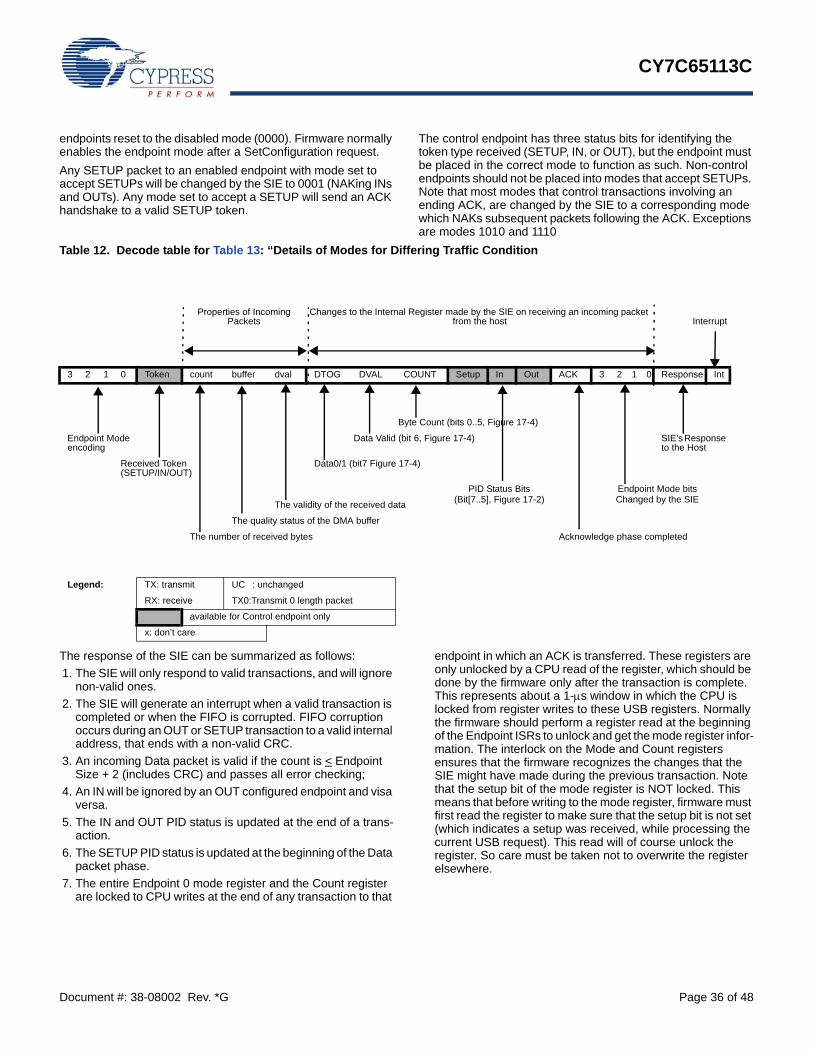
CY7C65113C
Document #: 38-08002 Rev. *G Page 36 of 48
endpoints reset to the disabled mode (0000). Firmware normally enables the endpoint mode after a SetConfiguration request.Any SETUP packet to an enabled endpoint with mode set to accept SETUPs will be changed by the SIE to 0001 (NAKing INs and OUTs). Any mode set to accept a SETUP will send an ACK handshake to a valid SETUP token.
The control endpoint has three status bits for identifying the token type received (SETUP, IN, or OUT), but the endpoint must be placed in the correct mode to function as such. Non-control endpoints should not be placed into modes that accept SETUPs. Note that most modes that control transactions involving an ending ACK, are changed by the SIE to a corresponding mode which NAKs subsequent packets following the ACK. Exceptions are modes 1010 and 1110.
The response of the SIE can be summarized as follows:1. The SIE will only respond to valid transactions, and will ignore
non-valid ones.2. The SIE will generate an interrupt when a valid transaction is
completed or when the FIFO is corrupted. FIFO corruption occurs during an OUT or SETUP transaction to a valid internal address, that ends with a non-valid CRC.
3. An incoming Data packet is valid if the count is < Endpoint Size + 2 (includes CRC) and passes all error checking;
4. An IN will be ignored by an OUT configured endpoint and visa versa.
5. The IN and OUT PID status is updated at the end of a trans-action.
6. The SETUP PID status is updated at the beginning of the Data packet phase.
7. The entire Endpoint 0 mode register and the Count register are locked to CPU writes at the end of any transaction to that
endpoint in which an ACK is transferred. These registers are only unlocked by a CPU read of the register, which should be done by the firmware only after the transaction is complete. This represents about a 1-μs window in which the CPU is locked from register writes to these USB registers. Normally the firmware should perform a register read at the beginning of the Endpoint ISRs to unlock and get the mode register infor-mation. The interlock on the Mode and Count registers ensures that the firmware recognizes the changes that the SIE might have made during the previous transaction. Note that the setup bit of the mode register is NOT locked. This means that before writing to the mode register, firmware must first read the register to make sure that the setup bit is not set (which indicates a setup was received, while processing the current USB request). This read will of course unlock the register. So care must be taken not to overwrite the register elsewhere.
Table 12. Decode table for Table 13: “Details of Modes for Differing Traffic Condition
Properties of Incoming Packets
Changes to the Internal Register made by the SIE on receiving an incoming packet from the host Interrupt
3 2 1 0 Token count buffer dval DTOG DVAL COUNT Setup In Out ACK 3 2 1 0 Response Int
Byte Count (bits 0..5, Figure 17-4)
SIE’s Response to the Host
Endpoint Mode encoding
Data Valid (bit 6, Figure 17-4)
Received Token (SETUP/IN/OUT)
Data0/1 (bit7 Figure 17-4)
PID Status Bits (Bit[7..5], Figure 17-2)
Endpoint Mode bits Changed by the SIEThe validity of the received data
The quality status of the DMA buffer
The number of received bytes Acknowledge phase completed
Legend: TX: transmit UC : unchanged
RX: receive TX0:Transmit 0 length packet
available for Control endpoint only
x: don’t care
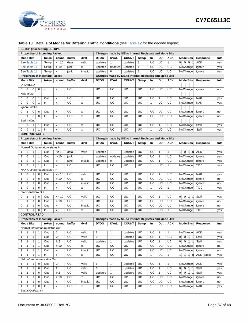
CY7C65113C
Document #: 38-08002 Rev. *G Page 37 of 48
.
Table 13. Details of Modes for Differing Traffic Conditions (see Table 12 for the decode legend)SETUP (if accepting SETUPs) Properties of Incoming Packet Changes made by SIE to Internal Registers and Mode Bits Mode Bits token count buffer dval DTOG DVAL COUNT Setup In Out ACK Mode Bits Response IntrSee Table 11 Setup <= 10 data valid updates 1 updates 1 UC UC 1 0 0 0 1 ACK yesSee Table 11 Setup > 10 junk x updates updates updates 1 UC UC UC NoChange ignore yesSee Table 11 Setup x junk invalid updates 0 updates 1 UC UC UC NoChange ignore yesProperties of Incoming Packet Changes made by SIE to Internal Registers and Mode Bits Mode Bits token count buffer dval DTOG DVAL COUNT Setup In Out ACK Mode Bits Response IntrDISABLED0 0 0 0 x x UC x UC UC UC UC UC UC UC NoChange ignore noNak In/Out0 0 0 1 Out x UC x UC UC UC UC UC 1 UC NoChange NAK yes0 0 0 1 In x UC x UC UC UC UC 1 UC UC NoChange NAK yesIgnore In/Out0 1 0 0 Out x UC x UC UC UC UC UC UC UC NoChange ignore no0 1 0 0 In x UC x UC UC UC UC UC UC UC NoChange ignore noStall In/Out0 0 1 1 Out x UC x UC UC UC UC UC 1 UC NoChange Stall yes0 0 1 1 In x UC x UC UC UC UC 1 UC UC NoChange Stall yesCONTROL WRITEProperties of Incoming Packet Changes made by SIE to Internal Registers and Mode Bits Mode Bits token count buffer dval DTOG DVAL COUNT Setup In Out ACK Mode Bits Response IntrNormal Out/premature status In1 0 1 1 Out <= 10 data valid updates 1 updates UC UC 1 1 1 0 1 0 ACK yes1 0 1 1 Out > 10 junk x updates updates updates UC UC 1 UC NoChange ignore yes1 0 1 1 Out x junk invalid updates 0 updates UC UC 1 UC NoChange ignore yes1 0 1 1 In x UC x UC UC UC UC 1 UC 1 NoChange TX 0 yesNAK Out/premature status In1 0 1 0 Out <= 10 UC valid UC UC UC UC UC 1 UC NoChange NAK yes1 0 1 0 Out > 10 UC x UC UC UC UC UC UC UC NoChange ignore no1 0 1 0 Out x UC invalid UC UC UC UC UC UC UC NoChange ignore no1 0 1 0 In x UC x UC UC UC UC 1 UC 1 NoChange TX 0 yesStatus In/extra Out0 1 1 0 Out <= 10 UC valid UC UC UC UC UC 1 UC 0 0 1 1 Stall yes0 1 1 0 Out > 10 UC x UC UC UC UC UC UC UC NoChange ignore no0 1 1 0 Out x UC invalid UC UC UC UC UC UC UC NoChange ignore no0 1 1 0 In x UC x UC UC UC UC 1 UC 1 NoChange TX 0 yesCONTROL READProperties of Incoming Packet Changes made by SIE to Internal Registers and Mode Bits Mode Bits token count buffer dval DTOG DVAL COUNT Setup In Out ACK Mode Bits Response IntrNormal In/premature status Out1 1 1 1 Out 2 UC valid 1 1 updates UC UC 1 1 NoChange ACK yes1 1 1 1 Out 2 UC valid 0 1 updates UC UC 1 UC 0 0 1 1 Stall yes1 1 1 1 Out !=2 UC valid updates 1 updates UC UC 1 UC 0 0 1 1 Stall yes1 1 1 1 Out > 10 UC x UC UC UC UC UC UC UC NoChange ignore no1 1 1 1 Out x UC invalid UC UC UC UC UC UC UC NoChange ignore no1 1 1 1 In x UC x UC UC UC UC 1 UC 1 1 1 1 0 ACK (back) yesNak In/premature status Out1 1 1 0 Out 2 UC valid 1 1 updates UC UC 1 1 NoChange ACK yes1 1 1 0 Out 2 UC valid 0 1 updates UC UC 1 UC 0 0 1 1 Stall yes1 1 1 0 Out !=2 UC valid updates 1 updates UC UC 1 UC 0 0 1 1 Stall yes1 1 1 0 Out > 10 UC x UC UC UC UC UC UC UC NoChange ignore no1 1 1 0 Out x UC invalid UC UC UC UC UC UC UC NoChange ignore no1 1 1 0 In x UC x UC UC UC UC 1 UC UC NoChange NAK yesStatus Out/extra In
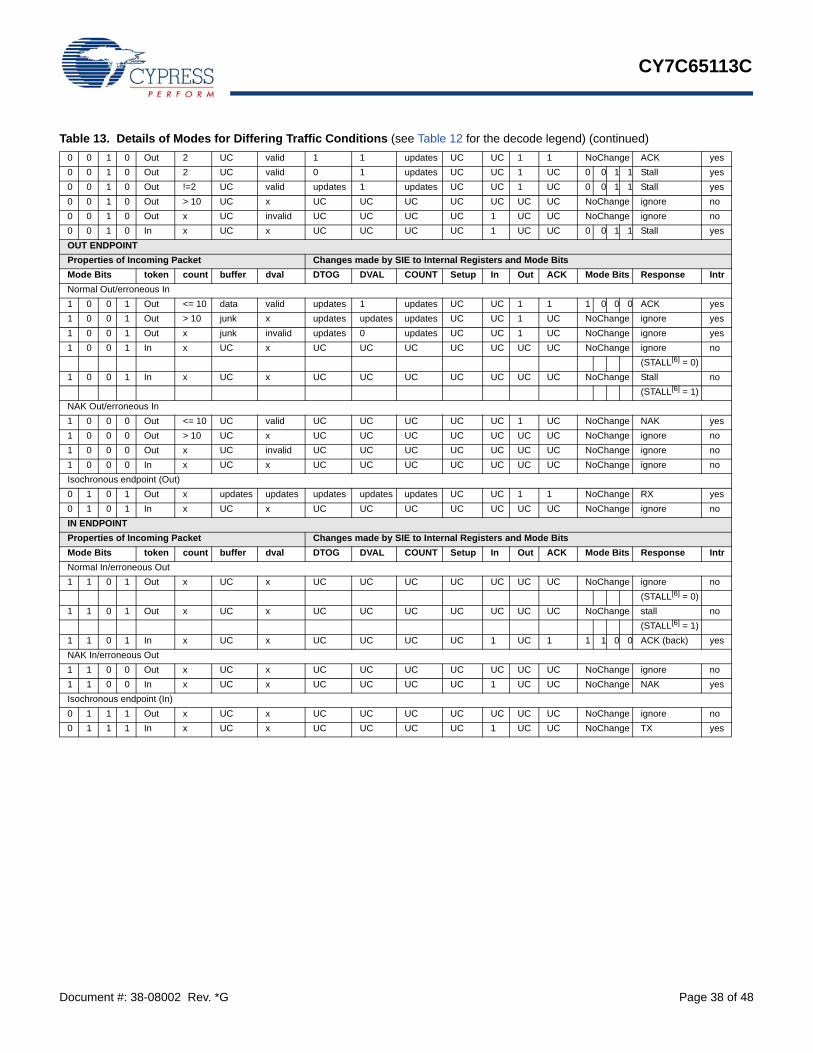
CY7C65113C
Document #: 38-08002 Rev. *G Page 38 of 48
0 0 1 0 Out 2 UC valid 1 1 updates UC UC 1 1 NoChange ACK yes0 0 1 0 Out 2 UC valid 0 1 updates UC UC 1 UC 0 0 1 1 Stall yes0 0 1 0 Out !=2 UC valid updates 1 updates UC UC 1 UC 0 0 1 1 Stall yes0 0 1 0 Out > 10 UC x UC UC UC UC UC UC UC NoChange ignore no0 0 1 0 Out x UC invalid UC UC UC UC 1 UC UC NoChange ignore no0 0 1 0 In x UC x UC UC UC UC 1 UC UC 0 0 1 1 Stall yesOUT ENDPOINTProperties of Incoming Packet Changes made by SIE to Internal Registers and Mode Bits Mode Bits token count buffer dval DTOG DVAL COUNT Setup In Out ACK Mode Bits Response IntrNormal Out/erroneous In1 0 0 1 Out <= 10 data valid updates 1 updates UC UC 1 1 1 0 0 0 ACK yes1 0 0 1 Out > 10 junk x updates updates updates UC UC 1 UC NoChange ignore yes1 0 0 1 Out x junk invalid updates 0 updates UC UC 1 UC NoChange ignore yes1 0 0 1 In x UC x UC UC UC UC UC UC UC NoChange ignore no
(STALL[6] = 0)1 0 0 1 In x UC x UC UC UC UC UC UC UC NoChange Stall no
(STALL[6] = 1)NAK Out/erroneous In1 0 0 0 Out <= 10 UC valid UC UC UC UC UC 1 UC NoChange NAK yes1 0 0 0 Out > 10 UC x UC UC UC UC UC UC UC NoChange ignore no1 0 0 0 Out x UC invalid UC UC UC UC UC UC UC NoChange ignore no1 0 0 0 In x UC x UC UC UC UC UC UC UC NoChange ignore noIsochronous endpoint (Out)0 1 0 1 Out x updates updates updates updates updates UC UC 1 1 NoChange RX yes0 1 0 1 In x UC x UC UC UC UC UC UC UC NoChange ignore noIN ENDPOINTProperties of Incoming Packet Changes made by SIE to Internal Registers and Mode Bits Mode Bits token count buffer dval DTOG DVAL COUNT Setup In Out ACK Mode Bits Response IntrNormal In/erroneous Out1 1 0 1 Out x UC x UC UC UC UC UC UC UC NoChange ignore no
(STALL[6] = 0)1 1 0 1 Out x UC x UC UC UC UC UC UC UC NoChange stall no
(STALL[6] = 1)1 1 0 1 In x UC x UC UC UC UC 1 UC 1 1 1 0 0 ACK (back) yesNAK In/erroneous Out1 1 0 0 Out x UC x UC UC UC UC UC UC UC NoChange ignore no1 1 0 0 In x UC x UC UC UC UC 1 UC UC NoChange NAK yesIsochronous endpoint (In)0 1 1 1 Out x UC x UC UC UC UC UC UC UC NoChange ignore no0 1 1 1 In x UC x UC UC UC UC 1 UC UC NoChange TX yes
Table 13. Details of Modes for Differing Traffic Conditions (see Table 12 for the decode legend) (continued)

CY7C65113C
Document #: 38-08002 Rev. *G Page 39 of 48
Register Summary Address Register Name Bit 7 Bit 6 Bit 5 Bit 4 Bit 3 Bit 2 Bit 1 Bit 0 Read/Write/B
oth/–[7]Default/Reset
G
PIO
CO
NFI
GU
RAT
ION
PO
RTS
0 A
ND
1 0x00 Port 0 Data P0.7 P0.6 P0.5 P0.4 P0.3 P0.2 P0.1 P0.0 BBBBBBBB 11111111
0x01 Port 1 Data P1.7 P1.6 P1.5 P1.4 P1.3 P1.2 P1.1 P1.0 BBBBBBBB 11111111
0x02 Port 2 Data P2.7 P2.6 P2.5 P2.4 P2.3 P2.2 P2.1 P2.0 BBBBBBBB 11111111
0x03 Port 3 Data P3.7 P3.6 P3.5 P3.4 P3.3 P3.2 P3.1 P3.0 BBBBBBBB 111111110x04 Port 0 Interrupt Enable P0.7 Intr
EnableP0.6 Intr Enable
P0.5 IntrEnable
P0.4 IntrEnable
P0.3 IntrEnable
P0.2 IntrEnable
P0.1 IntrEnable
P0.0 IntrEnable
WWWWWWWW 00000000
0x05 Port 1 Interrupt Enable P1.7 Intr Enable
P1.6 Intr Enable
P1.5 IntrEnable
P1.4 Intr Enable
Reserved P1.2 IntrEnable
P1.1 IntrEnable
P1.0 Intr Enable
WWWWWWWW 00000000
0x08 GPIO Configuration Reserved Reserved Reserved Reserved Port 1 Config Bit 1
Port 1 Config Bit 0
Port 0 Config Bit 1
Port 0 Config Bit 0
BBBBBBBB 00000000
HA
PII2 C
0x09 HAPI/I2C Configuration I2C Position Reserved Reserved Reserved Reserved Reserved I2C Port Width
Reserved BBBBBBBB 00000000
END
POIN
T A
0, A
I AN
D A
2 C
ON
FIG
UR
ATIO
N 0x10 USB Device Address A Device Address A
Enable
DeviceAddress A
Bit 6
DeviceAddress A
Bit 5
DeviceAddress A
Bit 4
DeviceAddress A
Bit 3
DeviceAddress A
Bit 2
DeviceAddress A
Bit 1
DeviceAddress A
Bit 0
BBBBBBBB 00000000
0x11 EP A0 CounterRegister
Data 0/1Toggle
Data Valid Byte CountBit 5
Byte CountBit 4
Byte CountBit 3
Byte CountBit 2
Byte CountBit 1
Byte CountBit 0
BBBBBBBB 00000000
0x12 EP A0 Mode Register Endpoint0SETUP
Received
Endpoint0IN
Received
Endpoint0 OUT
Received
ACK Mode Bit 3 Mode Bit 2 Mode Bit 1 Mode Bit 0 BBBBBBBB 00000000
0x13 EP A1 CounterRegister
Data 0/1Toggle
Data Valid Byte CountBit 5
Byte CountBit 4
Byte CountBit 3
Byte CountBit 2
Byte CountBit 1
Byte CountBit 0
BBBBBBBB 00000000
0x14 EP A1 Mode Register STALL - - ACK Mode Bit 3 Mode Bit 2 Mode Bit 1 Mode Bit 0 BBBBBBBB 00000000
0x15 EP A2 CounterRegister
Data 0/1Toggle
Data Valid Byte CountBit 5
Byte CountBit 4
Byte CountBit 3
Byte CountBit 2
Byte CountBit 1
Byte CountBit 0
BBBBBBBB 00000000
0x16 EP A2 Mode Register STALL - - ACK Mode Bit 3 Mode Bit 2 Mode Bit 1 Mode Bit 0 BBBBBBBB 00000000
USB
-C
S
0x1F USB Status and Control EndpointSize
Endpoint Mode
D+Upstream
D–Upstream
Bus Activity ControlBit 2
Control Bit 1
ControlBit 0
BBRRBBBB -0xx0000
INTE
RR
UPT
0x20 Global Interrupt Enable Reserved I2CInterrupt Enable
GPIOInterrupt Enable
Reserved USB HubInterruptEnable
1.024-msInterrupt Enable
128-μsInterrupt Enable
USB Bus RESET Interrupt Enable
-BBBBBBB -0000000
0x21 Endpoint Interrupt Enable
Reserved Reserved Reserved EPB1 Interrupt Enable
EPB0 Interrupt Enable
EPA2 Interrupt Enable
EPA1 Interrupt Enable
EPA0 Interrupt Enable
---BBBBB ---00000
TIM
ER
0x24 Timer (LSB) Timer Bit 7 Timer Bit 6 Timer Bit 5 Timer Bit 4 Timer Bit 3 Timer Bit 2 Timer Bit 1 Timer Bit 0 RRRRRRRR 00000000
0x25 Timer (MSB) Reserved Reserved Reserved Reserved Timer Bit 11 Timer Bit 10 Time Bit 9 Timer Bit 8 ----rrrr ----0000
I2 C
0x28 I2C Control and Status MSTRMode
Continue/Busy
XmitMode
ACK Addr ARB Lost/Restart
Received Stop
I2CEnable
BBBBBBBB 00000000
0x29 I2C Data I2C Data 7 I2C Data 6 I2C Data 5 I2C Data 4 I2C Data 3 I2C Data 2 I2C Data 1 I2C Data 0 BBBBBBBB XXXXXXXX
END
POIN
T B
0, B
1 C
ON
FIG
UR
ATIO
N 0x40 USB Device Address B Device Address B
Enable
DeviceAddress B
Bit 6
DeviceAddress B
Bit 5
DeviceAddress B
Bit 4
DeviceAddress B
Bit 3
DeviceAddress B
Bit 2
DeviceAddress B
Bit 1
Device Address B
Bit 0
BBBBBBBB 00000000
0x41 EP B0 Counter Register Data 0/1 Toggle
Data Valid Byte Count Bit 5
Byte Count Bit 4
Byte Count Bit 3
Byte Count Bit 2
Byte Count Bit 1
Byte Count Bit 0
BBBBBBBB 00000000
0x42 EP B0 Mode Register Endpoint 0SETUP
Received
Endpoint 0IN
Received
Endpoint 0OUT
Received
ACK Mode Bit 3 Mode Bit 2 Mode Bit 1 Mode Bit 0 BBBBBBBB 00000000
0x43 EP B1 Counter Register Data 0/1Toggle
Data Valid Byte CountBit 5
Byte CountBit 4
Byte CountBit 3
Byte CountBit 2
Byte CountBit 1
Byte CountBit 0
BBBBBBBB 00000000
0x44 EP B1 Mode Register STALL - - ACK Mode Bit 3 Mode Bit 2 Mode Bit 1 Mode Bit 0 BBBBBBBB 00000000
Note7. B: Read and Write; W: Write; R: Read.
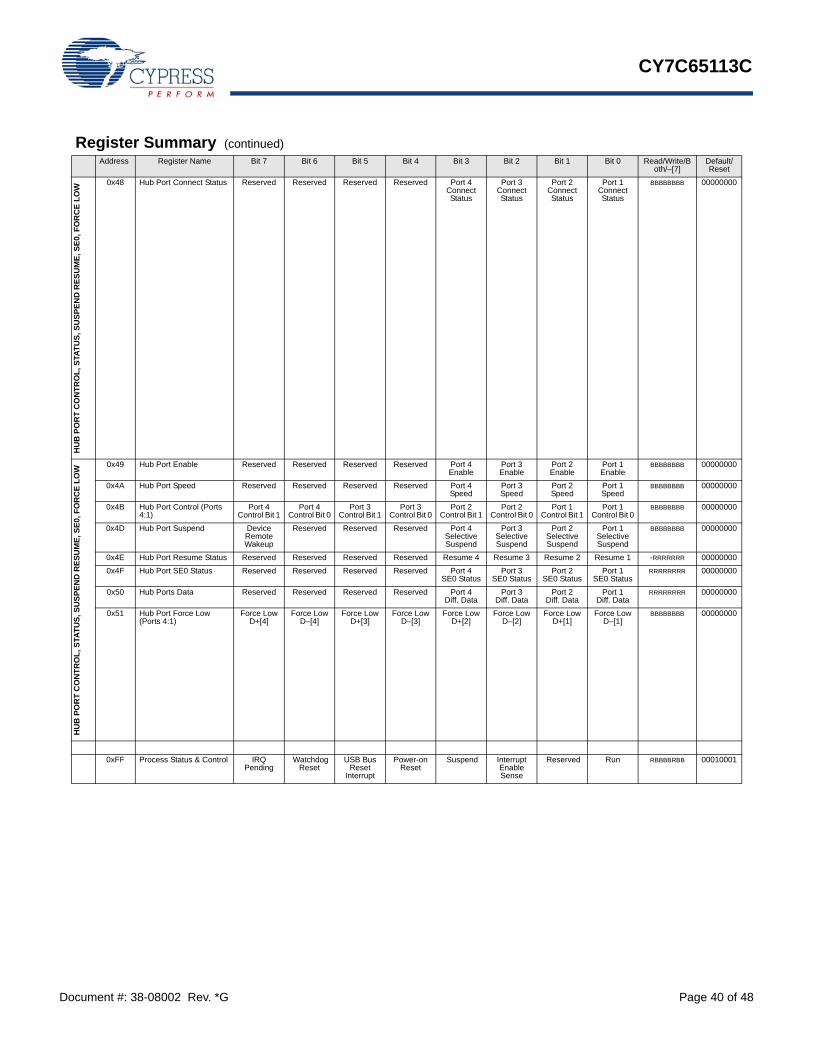
CY7C65113C
Document #: 38-08002 Rev. *G Page 40 of 48
HU
B P
OR
T C
ON
TRO
L, S
TATU
S, S
USP
END
RES
UM
E, S
E0, F
OR
CE
LOW
0x48 Hub Port Connect Status Reserved Reserved Reserved Reserved Port 4 Connect Status
Port 3 Connect Status
Port 2 Connect Status
Port 1 Connect Status
BBBBBBBB 00000000
HU
B P
OR
T C
ON
TRO
L, S
TATU
S, S
USP
END
RES
UM
E, S
E0, F
OR
CE
LOW
0x49 Hub Port Enable Reserved Reserved Reserved Reserved Port 4Enable
Port 3Enable
Port 2Enable
Port 1Enable
BBBBBBBB 00000000
0x4A Hub Port Speed Reserved Reserved Reserved Reserved Port 4Speed
Port 3Speed
Port 2Speed
Port 1Speed
BBBBBBBB 00000000
0x4B Hub Port Control (Ports 4:1)
Port 4Control Bit 1
Port 4Control Bit 0
Port 3Control Bit 1
Port 3Control Bit 0
Port 2Control Bit 1
Port 2Control Bit 0
Port 1Control Bit 1
Port 1Control Bit 0
BBBBBBBB 00000000
0x4D Hub Port Suspend Device Remote Wakeup
Reserved Reserved Reserved Port 4 Selective Suspend
Port 3Selective Suspend
Port 2SelectiveSuspend
Port 1Selective Suspend
BBBBBBBB 00000000
0x4E Hub Port Resume Status Reserved Reserved Reserved Reserved Resume 4 Resume 3 Resume 2 Resume 1 -RRRRRRR 00000000
0x4F Hub Port SE0 Status Reserved Reserved Reserved Reserved Port 4 SE0 Status
Port 3SE0 Status
Port 2SE0 Status
Port 1SE0 Status
RRRRRRRR 00000000
0x50 Hub Ports Data Reserved Reserved Reserved Reserved Port 4Diff. Data
Port 3Diff. Data
Port 2Diff. Data
Port 1Diff. Data
RRRRRRRR 00000000
0x51 Hub Port Force Low (Ports 4:1)
Force LowD+[4]
Force LowD–[4]
Force LowD+[3]
Force Low D–[3]
Force LowD+[2]
Force LowD–[2]
Force LowD+[1]
Force LowD–[1]
BBBBBBBB 00000000
0xFF Process Status & Control IRQPending
Watchdog Reset
USB Bus Reset
Interrupt
Power-on Reset
Suspend InterruptEnable Sense
Reserved Run RBBBBRBB 00010001
Register Summary (continued)Address Register Name Bit 7 Bit 6 Bit 5 Bit 4 Bit 3 Bit 2 Bit 1 Bit 0 Read/Write/B
oth/–[7]Default/Reset
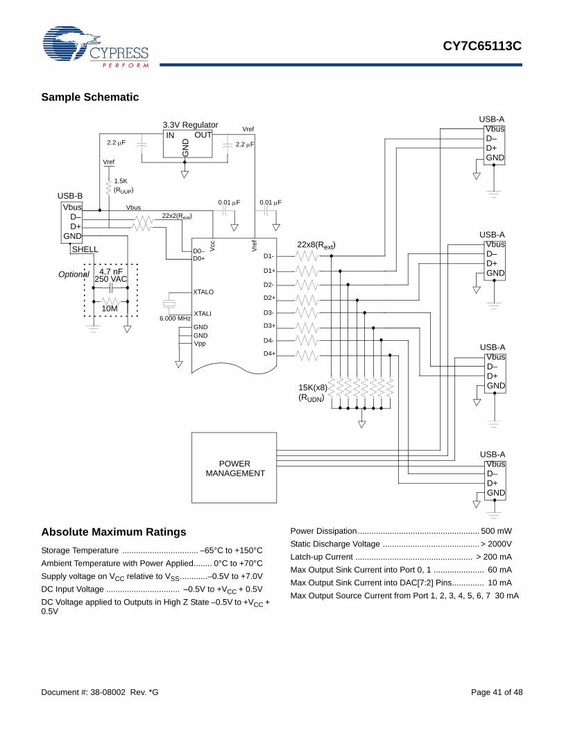
CY7C65113C
Document #: 38-08002 Rev. *G Page 41 of 48
Sample Schematic
Absolute Maximum RatingsStorage Temperature ................................. –65°C to +150°CAmbient Temperature with Power Applied........ 0°C to +70°CSupply voltage on VCC relative to VSS............–0.5V to +7.0VDC Input Voltage ................................ –0.5V to +VCC + 0.5VDC Voltage applied to Outputs in High Z State –0.5V to +VCC + 0.5V
Power Dissipation..................................................... 500 mWStatic Discharge Voltage .......................................... > 2000VLatch-up Current ................................................... > 200 mAMax Output Sink Current into Port 0, 1 ...................... 60 mAMax Output Sink Current into DAC[7:2] Pins.............. 10 mAMax Output Source Current from Port 1, 2, 3, 4, 5, 6, 7 30 mA
XTALO
XTALI
D0–D0+
D1+
D1-
D2-
D2+
D3-
D3+
D4-
D4+
Vcc
Vref
Vpp
GNDGND
IN
GN
D
OUT
USB-BVbus
D–D+
GND
0.01 μF
6.000 MHz
22x2(Rext)Vbus
Vref
Vref
0.01 μF
2.2 μF2.2 μF
1.5K
SHELL
10M
4.7 nF250 VAC
POWERMANAGEMENT
USB-AVbusD–D+GND
USB-AVbusD–D+GND
USB-AVbusD–D+GND
USB-AVbusD–D+GND
15K(x8)
22x8(Rext)
Optional
3.3V Regulator
(RUUP)
(RUDN)
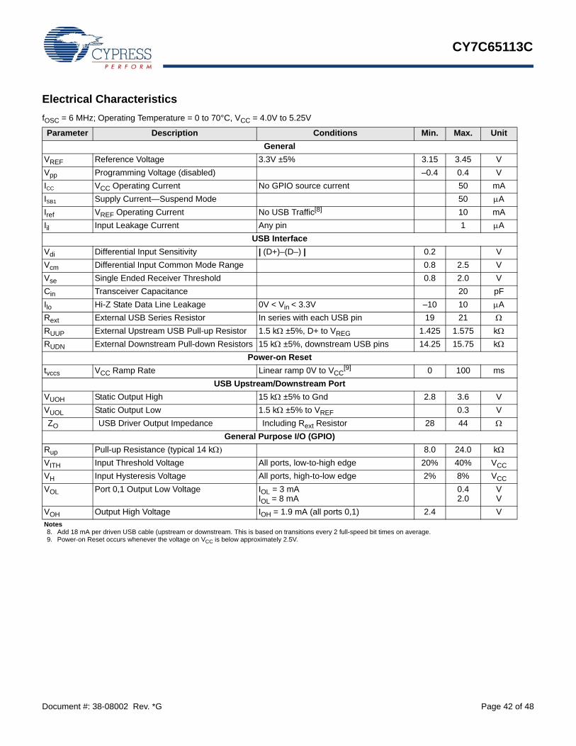
CY7C65113C
Document #: 38-08002 Rev. *G Page 42 of 48
Electrical CharacteristicsfOSC = 6 MHz; Operating Temperature = 0 to 70°C, VCC = 4.0V to 5.25V
Parameter Description Conditions Min. Max. UnitGeneral
VREF Reference Voltage 3.3V ±5% 3.15 3.45 VVpp Programming Voltage (disabled) –0.4 0.4 VICC VCC Operating Current No GPIO source current 50 mAISB1 Supply Current—Suspend Mode 50 μAIref VREF Operating Current No USB Traffic[8] 10 mAIil Input Leakage Current Any pin 1 μA
USB InterfaceVdi Differential Input Sensitivity | (D+)–(D–) | 0.2 VVcm Differential Input Common Mode Range 0.8 2.5 VVse Single Ended Receiver Threshold 0.8 2.0 VCin Transceiver Capacitance 20 pFIlo Hi-Z State Data Line Leakage 0V < Vin < 3.3V –10 10 μARext External USB Series Resistor In series with each USB pin 19 21 Ω
RUUP External Upstream USB Pull-up Resistor 1.5 kΩ ±5%, D+ to VREG 1.425 1.575 kΩ
RUDN External Downstream Pull-down Resistors 15 kΩ ±5%, downstream USB pins 14.25 15.75 kΩ
Power-on Resettvccs VCC Ramp Rate Linear ramp 0V to VCC
[9] 0 100 msUSB Upstream/Downstream Port
VUOH Static Output High 15 kΩ ±5% to Gnd 2.8 3.6 VVUOL Static Output Low 1.5 kΩ ±5% to VREF 0.3 VZO USB Driver Output Impedance Including Rext Resistor 28 44 Ω
General Purpose I/O (GPIO)Rup Pull-up Resistance (typical 14 kΩ) 8.0 24.0 kΩ
VITH Input Threshold Voltage All ports, low-to-high edge 20% 40% VCCVH Input Hysteresis Voltage All ports, high-to-low edge 2% 8% VCCVOL Port 0,1 Output Low Voltage IOL = 3 mA
IOL = 8 mA0.42.0
VV
VOH Output High Voltage IOH = 1.9 mA (all ports 0,1) 2.4 VNotes8. Add 18 mA per driven USB cable (upstream or downstream. This is based on transitions every 2 full-speed bit times on average.9. Power-on Reset occurs whenever the voltage on VCC is below approximately 2.5V.
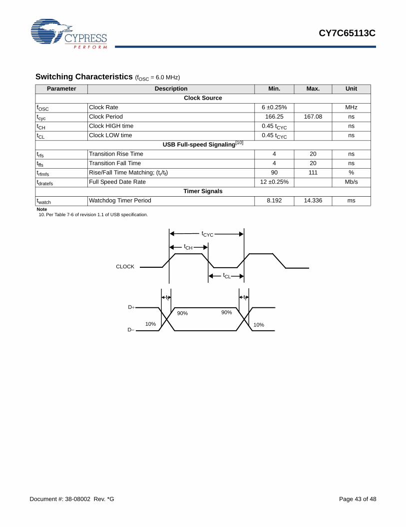
CY7C65113C
Document #: 38-08002 Rev. *G Page 43 of 48
Switching Characteristics (fOSC = 6.0 MHz) Parameter Description Min. Max. Unit
Clock SourcefOSC Clock Rate 6 ±0.25% MHztcyc Clock Period 166.25 167.08 nstCH Clock HIGH time 0.45 tCYC nstCL Clock LOW time 0.45 tCYC ns
USB Full-speed Signaling[10]
trfs Transition Rise Time 4 20 nstffs Transition Fall Time 4 20 nstrfmfs Rise/Fall Time Matching; (tr/tf) 90 111 %tdratefs Full Speed Date Rate 12 ±0.25% Mb/s
Timer Signalstwatch Watchdog Timer Period 8.192 14.336 msNote10. Per Table 7-6 of revision 1.1 of USB specification.
CLOCK
tCYC
tCL
tCH
90%
10%
90%
10%D−
D+
tr tr
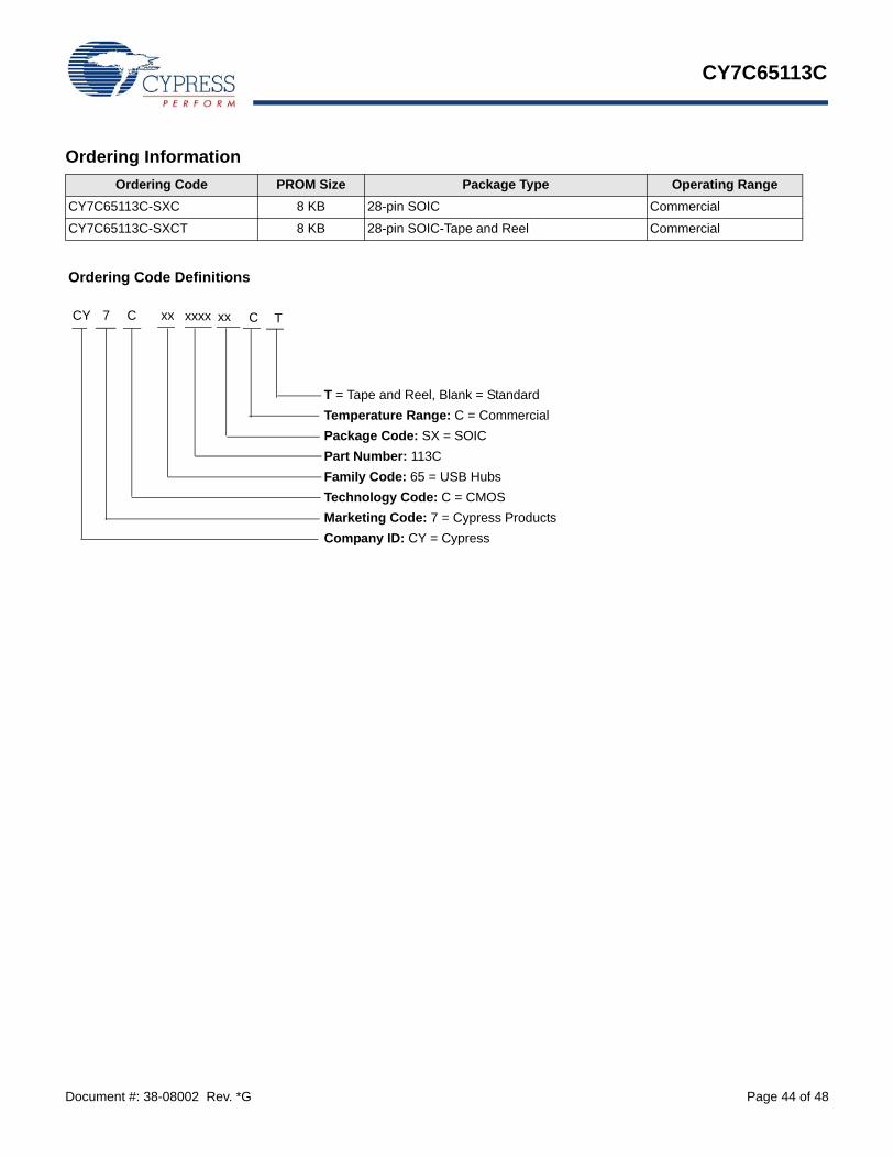
CY7C65113C
Document #: 38-08002 Rev. *G Page 44 of 48
Ordering InformationOrdering Code PROM Size Package Type Operating Range
CY7C65113C-SXC 8 KB 28-pin SOIC Commercial
CY7C65113C-SXCT 8 KB 28-pin SOIC-Tape and Reel Commercial
Ordering Code Definitions
T = Tape and Reel, Blank = StandardTemperature Range: C = CommercialPackage Code: SX = SOICPart Number: 113CFamily Code: 65 = USB HubsTechnology Code: C = CMOSMarketing Code: 7 = Cypress ProductsCompany ID: CY = Cypress
7CY C xx Txxxx xx C

CY7C65113C
Document #: 38-08002 Rev. *G Page 45 of 48
Package DiagramFigure 36. 28-Pin (300-Mil) Molded SOIC
51-85026 *H
CY7C65113C
Document #: 38-08002 Rev. *G Page 46 of 48
Acronyms Document ConventionsUnits of MeasureAcronym Description
CMOS complementary metal oxide semiconductorCPU central processing unitDSP data stack pointerEMI electro magnetic interferenceGPIO general purpose I/OHID human interface deviceI2C inter integrated circuitLSB least-significant byteMSB most-significant bytePC program counterPLL phase-locked loopPOR power on resetPROM precision power on resetPSP program stack pointerRAM random access memorySIE serial interface engineSOIC small outlined integrated circuitSRAM standard random access memoryUSB universal serial busWDT watchdog timer
Convention DescriptionDC Direct currentKB 1024 bytesKbit 1024 bitskHz kilohertzkΩ kilohmmA milli-ampere
Mbps megabits per secondms milli secondspF picofaradμs microsecondV volts
CY7C65113C
Document #: 38-08002 Rev. *G Page 47 of 48
Document History Page
Document Title: CY7C65113C USB Hub with MicrocontrollerDocument Number: 38-08002
REV. ECN NO. Issue Date Orig. of Change Description of Change
** 109965 02/22/02 SZV Change from Spec number: 38-00590 to 38-08002*A 120372 12/17/02 MON Added register bit definitions.
Added default bit state of each register.Corrected the Schematic (location of the pull-up on D+).Corrected the Logical Diagram (removed the extra GPIO Port 1).Added register summary.Modified Figure 17, more labeling.Removed information on the availability of the part in PDIP package.Modified Table 11 and provided more explanation regarding locking/unlocking mechanism of the mode register.Removed any information regarding the speed detect bit in Hub Port Speed register being set by hardware.
*B 124522 03/13/03 MON Fixed the figure on page 42 regarding the update of mode registers. The arrows in the figure were misplaced and the figure was unreadable. This is an important figure for understanding mode register functioning.
*C 368601 See ECN BHA Added Lead-free Package Information.Removed CY7C65013 Information.Updated Package Drawing.
*D 429098 See ECN TYJ Part numbers changed to ‘C’ typesCypress Perform logo addedPart numbers updated in the ordering section
*E 3057657 10/13/10 AJHA Added “Not recommended for new designs” watermark in the PDF.Updated package diagrams.Updated template.
*F 3207401 03/28/2011 ODC Added Ordering Code Definitions, Acronyms, and Document Conventions. Updated package diagram.
*G 4313900 03/21/2014 AKSL Removed "Not recommended for new designs" watermark.Updated package diagram to current revision.
Document #: 38-08002 Rev. *G Revised March 21, 2014 Page 48 of 48
Purchase of I2C components from Cypress, or one of its sublicensed Associated Companies, conveys a license under the Philips I2C Patent Rights to use these components in an I2C system, providedthat the system conforms to the I2C Standard Specification as defined by Philips. All product and company names mentioned in this document are the trademarks of their respective holders.
CY7C65113C
© Cypress Semiconductor Corporation, 2002-2014. The information contained herein is subject to change without notice. Cypress Semiconductor Corporation assumes no responsibility for the use ofany circuitry other than circuitry embodied in a Cypress product. Nor does it convey or imply any license under patent or other rights. Cypress products are not warranted nor intended to be used formedical, life support, life saving, critical control or safety applications, unless pursuant to an express written agreement with Cypress. Furthermore, Cypress does not authorize its products for use ascritical components in life-support systems where a malfunction or failure may reasonably be expected to result in significant injury to the user. The inclusion of Cypress products in life-support systemsapplication implies that the manufacturer assumes all risk of such use and in doing so indemnifies Cypress against all charges.
Any Source Code (software and/or firmware) is owned by Cypress Semiconductor Corporation (Cypress) and is protected by and subject to worldwide patent protection (United States and foreign),United States copyright laws and international treaty provisions. Cypress hereby grants to licensee a personal, non-exclusive, non-transferable license to copy, use, modify, create derivative works of,and compile the Cypress Source Code and derivative works for the sole purpose of creating custom software and or firmware in support of licensee product to be used only in conjunction with a Cypressintegrated circuit as specified in the applicable agreement. Any reproduction, modification, translation, compilation, or representation of this Source Code except as specified above is prohibited withoutthe express written permission of Cypress.
Disclaimer: CYPRESS MAKES NO WARRANTY OF ANY KIND, EXPRESS OR IMPLIED, WITH REGARD TO THIS MATERIAL, INCLUDING, BUT NOT LIMITED TO, THE IMPLIED WARRANTIESOF MERCHANTABILITY AND FITNESS FOR A PARTICULAR PURPOSE. Cypress reserves the right to make changes without further notice to the materials described herein. Cypress does notassume any liability arising out of the application or use of any product or circuit described herein. Cypress does not authorize its products for use as critical components in life-support systems wherea malfunction or failure may reasonably be expected to result in significant injury to the user. The inclusion of Cypress’ product in a life-support systems application implies that the manufacturerassumes all risk of such use and in doing so indemnifies Cypress against all charges.
Use may be limited by and subject to the applicable Cypress software license agreement.
Sales, Solutions, and Legal InformationWorldwide Sales and Design SupportCypress maintains a worldwide network of offices, solution centers, manufacturer’s representatives, and distributors. To find the office closest to you, visit us at Cypress Locations.
ProductsAutomotive cypress.com/go/automotiveClocks & Buffers cypress.com/go/clocksInterface cypress.com/go/interfaceLighting & Power Control cypress.com/go/powerpsoc
cypress.com/go/plcMemory cypress.com/go/memoryPSoC cypress.com/go/psocTouch Sensing cypress.com/go/touchUSB Controllers cypress.com/go/USBWireless/RF cypress.com/go/wireless
PSoC® Solutionspsoc.cypress.com/solutionsPSoC 1 | PSoC 3 | PSoC 4 | PSoC 5LP
Cypress Developer CommunityCommunity | Forums | Blogs | Video | Training
Technical Supportcypress.com/go/support