cy7c026a, 16 k × 16 dual-port static ram · cy7c026a 16 k × 16 dual-port static ram ... 4...
TRANSCRIPT
CY7C026A
16 K × 16 Dual-Port Static RAM
Cypress Semiconductor Corporation • 198 Champion Court • San Jose, CA 95134-1709 • 408-943-2600Document Number: 38-06046 Rev. *H Revised October 31, 2012
16 K × 16 Dual-Port Static RAM
Features
■ True dual-ported memory cells that allow simultaneous access of the same memory location
■ 16 K × 16 organization (CY7C026A)
■ 0.35 micron CMOS for optimum speed and power
■ High speed access: 15, and 20 ns
■ Low operating power
■ Active: ICC = 180 mA (typical)
■ Standby: ISB3 = 0.05 mA (typical)
■ Fully asynchronous operation
■ Automatic power-down
■ Expandable data bus to 32 bits or more using Master/Slave chip select when using more than one device
■ On-chip arbitration logic
■ Semaphores included to permit software handshaking between ports
■ INT flags for port-to-port communication
■ Separate upper-byte and lower-byte control
■ Pin select for Master or Slave
■ Commercial and Industrial temperature ranges
■ Available in 100-pin thin quad plastic flatpack (TQFP)
■ Pb-free packages available
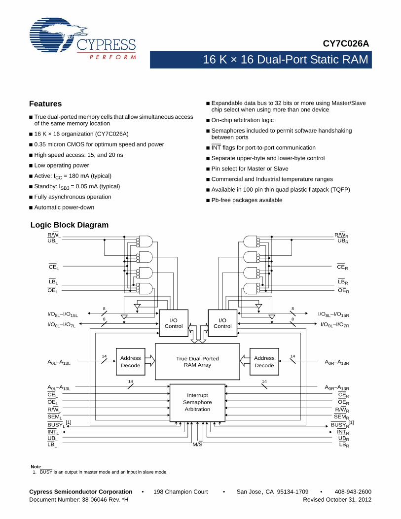
R/WL
OEL
I/O8L–I/O15LI/O
Control
Address
Decode
A0L–A13L
CEL
OEL
R/WL
BUSYL
I/OControl
CEL
InterruptSemaphoreArbitration
SEML
INTL
M/S
UBL
LBL
I/O0L–I/O7L
R/WR
OER
I/O8L–I/O15R
CER
UBR
LBR
I/O0L–I/O7R
UBLLBL
A0L–A13LTrue Dual-Ported
RAM Array
A0R–A13R
CER
OER
R/WR
BUSYR
SEMR
INTRUBRLBR
Address
DecodeA0R–A13R
[1] [1]
14
8
8
14
8
8
14 14
Logic Block Diagram
Note1. BUSY is an output in master mode and an input in slave mode.
CY7C026A16 K × 16 Dual-Port Static RAM
CY7C026A
Document Number: 38-06046 Rev. *H Page 2 of 24
Contents
Pin Configurations ........................................................... 3Pin Definitions .................................................................. 4Selection Guide ................................................................ 4Architecture ...................................................................... 5Functional Description ..................................................... 5
Write Operation ........................................................... 5Read Operation ........................................................... 5Interrupts ..................................................................... 5Busy ............................................................................ 5Master/Slave ............................................................... 5Semaphore Operation ................................................. 5
Maximum Ratings ............................................................. 7Operating Range ............................................................... 7Electrical Characteristics ................................................. 7Capacitance ...................................................................... 8AC Test Loads and Waveforms ....................................... 8Data Retention Mode ........................................................ 9Timing ................................................................................ 9
Switching Characteristics .............................................. 10Switching Waveforms .................................................... 12Non-Contending Read/Write .......................................... 18Interrupt Operation Example ......................................... 18Semaphore Operation Example .................................... 19Ordering Information ...................................................... 20
16 K × 16 Asynchronous Dual-Port SRAM ............... 20Ordering Code Definitions ......................................... 20
Package Diagram ............................................................ 21Acronyms ........................................................................ 22Document Conventions ................................................. 22
Units of Measure ....................................................... 22Document History Page ................................................. 23Sales, Solutions, and Legal Information ...................... 24
Worldwide Sales and Design Support ....................... 24Products .................................................................... 24PSoC Solutions ......................................................... 24
CY7C026A
Document Number: 38-06046 Rev. *H Page 3 of 24
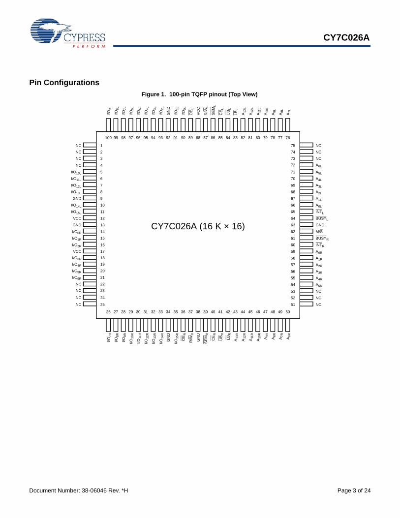
Pin Configurations
Figure 1. 100-pin TQFP pinout (Top View)
1
3
2
92 91 90 848587 868889 83 82 81 7678 77798093949596979899100
59
60
61
67
66
64
65
63
62
68
69
70
75
73
74
72
71
NC
NC
NC
A6L
A5L
A4L
INTL
A2L
A0L
GND
M/S
A0R
A1R
A1L
A3L
BUSYR
INTR
A2R
A3R
A4R
A5R
NC
NC
NC
BUSYL
58
57
56
55
54
53
52
51
CY7C026A (16 K × 16)
NC
NC
NC
NC
I/O10L
I/O11L
I/O15L
I/O13L
I/O14L
GND
I/O0R
VCC
I/O3R
GND
I/O12L
I/O1R
I/O2R
I/O4R
I/O5R
I/O6R
NC
NC
NC
NC
VCC
17
16
15
9
10
12
11
13
14
8
7
6
4
5
18
19
20
21
22
23
24
25
I/O
9L
I/O
8L
I/O
7L
I/O
6L
I/O
5L
I/O
4L
I/O
0L
I/O
2L
I/O
1L
VC
C
R/W
L
UB
L
LB
L
GN
D
I/O
3L
SE
ML
CE
L
A13
L
A12
L
A11
L
A10
L
A9L
A8L
A7L
OE
L
34 35 36 424139 403837 43 44 45 5048 494746
A6
R
A7
R
A8
R
A9
R
A10
R
A11
R
CE
R
A13
R
UB
R
GN
D
R/W
R
GN
D
I/O14
R
LBR
A12
R
OE
R
I/O15
R
I/O13
R
I/O12
R
I/O11
R
I/O10
R
I/O
9R
I/O
8R
I/O
7R
SE
MR
3332313029282726
CY7C026A
Document Number: 38-06046 Rev. *H Page 4 of 24
Pin DefinitionsLeft Port Right Port Description
CEL CER Chip enable
R/WL R/WR Read/Write enable
OEL OER Output enable
A0L–A13L A0R–A13R Address
I/O0L–I/O15L I/O0R–I/O15R Data bus input/output
SEML SEMR Semaphore enable
UBL UBR Upper byte select (I/O8–I/O15 for × 16 devices)
LBL LBR Lower byte select (I/O0–I/O7 for × 16 devices)
INTL INTR Interrupt flag
BUSYL BUSYR Busy flag
M/S Master or slave select
VCC Power
GND Ground
NC No connect
Selection Guide
Parameter CY7C026A-15
CY7C026A-20 Unit
Maximum access time 15 20 ns
Typical operating current 190 180 mA
Typical standby current for ISB1 (Both ports TTL level) 50 45 mA
Typical standby current for ISB3 (Both ports CMOS level) 0.05 0.05 mA
CY7C026A
Document Number: 38-06046 Rev. *H Page 5 of 24
Architecture
The CY7C026A consists of an array of 16K words of 16 bits eachof dual-port RAM cells, I/O and address lines, and control signals(CE, OE, R/W). These control pins permit independent accessfor reads or writes to any location in memory. To handlesimultaneous writes/reads to the same location, a BUSY pin isprovided on each port. Two Interrupt (INT) pins can be utilizedfor port-to-port communication. Two Semaphore (SEM) controlpins are used for allocating shared resources. With the M/S pin,the devices can function as a master (BUSY pins are outputs) oras a slave (BUSY pins are inputs). The devices also have anautomatic power down feature controlled by CE. Each port isprovided with its own Output Enable control (OE), which allowsdata to be read from the device.
Functional Description
The CY7C026A is a low power CMOS 16 K × 16 dual-port staticRAM. Various arbitration schemes are included on the devicesto handle situations when multiple processors access the samepiece of data. Two ports are provided, permitting independent,asynchronous access for reads and writes to any location inmemory. The device can be utilized as standalone 16-bitdual-port static RAM or multiple devices can be combined tofunction as a 32-bit or wider master/slave dual-port static RAM.An M/S pin is provided for implementing 32-bit or wider memoryapplications without the need for separate master and slavedevices or additional discrete logic. Application areas includeinterprocessor/multiprocessor designs, communications statusbuffering, and dual-port video/graphics memory.
Each port has independent control pins: Chip Enable (CE), Reador Write Enable (R/W), and Output Enable (OE). Two flags areprovided on each port (BUSY and INT). BUSY signals that theport is trying to access the same location currently beingaccessed by the other port. The Interrupt flag (INT) permitscommunication between ports or systems by means of a mailbox. The semaphores are used to pass a flag, or token, from oneport to the other to indicate that a shared resource is in use. Thesemaphore logic is comprised of eight shared latches. Only oneside can control the latch (semaphore) at any time. Control of asemaphore indicates that a shared resource is in use. Anautomatic power down feature is controlled independently oneach port by the chip enable pin.
The CY7C026A is available in 100-pin thin quad plastic flatpack(TQFP) packages.
Write Operation
Data must be set up for a duration of tSD before the rising edgeof R/W to either the R/W pin (see Figure 6 on page 13) or the CEpin (see Figure 7 on page 13). Required inputs fornon-contention operations are summarized in Non-ContendingRead/Write on page 18.
If a location is being written to by one port and the opposite portattempts to read that location, a port-to-port flowthrough delaymust occur before the data is read on the output; otherwise thedata read is not deterministic. Data is valid on the port tDDD afterthe data is presented on the other port.
Read Operation
When reading the device, the user must assert both the OE andCE pins. Data is available tACE after CE or tDOE after OE isasserted. If the user wishes to access a semaphore flag, then theSEM pin must be asserted instead of the CE pin, and OE mustalso be asserted.
Interrupts
The upper two memory locations may be used for messagepassing. The highest memory location (3FFF) is the mailbox forthe right port and the second highest memory location (3FFE) isthe mailbox for the left port. When one port writes to the otherport’s mailbox, an interrupt is generated to the owner. Theinterrupt is reset when the owner reads the contents of themailbox. The message is user defined.
Each port can read the other port’s mailbox without resetting theinterrupt. The active state of the busy signal (to a port) preventsthe port from setting the interrupt to the winning port. Also, anactive busy to a port prevents that port from reading its ownmailbox and, thus, resetting the interrupt to it.
If an application does not require message passing, do notconnect the interrupt pin to the processor’s interrupt requestinput pin.
The operation of the interrupts and their interaction with Busy aresummarized in Interrupt Operation Example on page 18.
Busy
The CY7C026A provides on-chip arbitration to resolvesimultaneous memory location access (contention). If both ports’CEs are asserted and an address match occurs within tPS ofeach other, the busy logic determines which port has access. IftPS is violated, one port definitely gains permission to thelocation, but it is not predictable which port gets that permission.BUSY is asserted tBLA after an address match or tBLC after CEis taken LOW.
Master/Slave
A M/S pin is provided to expand the word width by configuringthe device as either a master or a slave. The BUSY output of themaster is connected to the BUSY input of the slave. This allowsthe device to interface to a master device with no externalcomponents. Writing to slave devices must be delayed until afterthe BUSY input has settled (tBLC or tBLA), otherwise, the slavechip may begin a write cycle during a contention situation. Whentied HIGH, the M/S pin allows the device to be used as a masterand, therefore, the BUSY line is an output. BUSY can then beused to send the arbitration outcome to a slave.
Semaphore Operation
The CY7C026A provides eight semaphore latches, which areseparate from the dual-port memory locations. Semaphores areused to reserve resources that are shared between the two ports.The state of the semaphore indicates that a resource is in use.For example, if the left port wants to request a given resource, itsets a latch by writing a zero to a semaphore location. The leftport then verifies its success in setting the latch by reading it.After writing to the semaphore, SEM or OE must be deassertedfor tSOP before attempting to read the semaphore. Thesemaphore value is available tSWRD + tDOE after the rising edgeof the semaphore write. If the left port was successful (reads a
CY7C026A
Document Number: 38-06046 Rev. *H Page 6 of 24
zero), it assumes control of the shared resource, otherwise(reads a one) it assumes the right port has control and continuesto poll the semaphore. When the right side has relinquishedcontrol of the semaphore (by writing a one), the left sidesucceeds in gaining control of the semaphore. If the left side nolonger requires the semaphore, a one is written to cancel itsrequest.
Semaphores are accessed by asserting SEM LOW. The SEMpin functions as a chip select for the semaphore latches (CEmust remain HIGH during SEM LOW). A0–2 represents thesemaphore address. OE and R/W are used in the same manneras a normal memory access. When writing or reading asemaphore, the other address pins have no effect.
When writing to the semaphore, only I/O0 is used. If a zero iswritten to the left port of an available semaphore, a one appearsat the same semaphore address on the right port. That
semaphore can now only be modified by the side showing zero(the left port in this case). If the left port now relinquishes controlby writing a one to the semaphore, the semaphore is set to onefor both sides. However, if the right port had requested thesemaphore (written a zero) while the left port had control, theright port would immediately own the semaphore as soon as theleft port released it. Semaphore Operation Example on page 19shows sample semaphore operations.
When reading a semaphore, all sixteen/eighteen data linesoutput the semaphore value. The read value is latched in anoutput register to prevent the semaphore from changing stateduring a write from the other port. If both ports attempt to accessthe semaphore within tSPS of each other, the semaphore isdefinitely obtained by one side or the other, but there is noguarantee which side controls the semaphore.
CY7C026A
Document Number: 38-06046 Rev. *H Page 7 of 24
Maximum Ratings
Exceeding maximum ratings [2] may shorten the useful life of thedevice. User guidelines are not tested.
Storage temperature ................................ –65 °C to +150 °C
Ambient temperature with power applied .......................................... –55°C to +125 °C
Supply voltage to ground potential ..............–0.3 V to +7.0 V
DC voltage applied to outputs in High Z state .............................................–0.5 V to +7.0 V
DC input voltage [3] .....................................–0.5 V to + 7.0 V
Output current into outputs (LOW) ............................. 20 mA
Static discharge voltage .......................................... >2001 V
Latch-up current .................................................... >200 mA
Operating Range
Range Ambient Temperature VCC
Commercial 0 °C to +70 °C 5 V 10%
Industrial –40 °C to +85 °C 5 V 10%
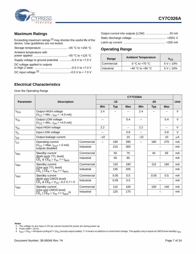
Electrical Characteristics
Over the Operating Range
Parameter Description
CY7C026A
Unit-15 -20
Min Typ Max Min Typ Max
VOH Output HIGH voltage (VCC = Min., IOH = –4.0 mA)
2.4 – – 2.4 – – V
VOL Output LOW voltage (VCC = Min., IOH = +4.0 mA)
– 0.4 – 0.4 V
VIH Input HIGH voltage 2.2 – 2.2 – V
VIL Input LOW voltage – 0.8 – 0.8 V
IOZ Output leakage current –10 10 –10 10 A
ICC Operating current (VCC = Max, IOUT = 0 mA) outputs disabled
Commercial – 190 285 – 180 275 mA
Industrial 215 305 – mA
ISB1 Standby current (Both ports TTL level) CEL & CER VIH, f = fMAX
Commercial 50 70 45 65 mA
Industrial 65 95 – mA
ISB2 Standby current (One port TTL level) CEL | CER VIH, f = fMAX
Commercial 120 180 110 160 mA
Industrial 135 205 – mA
ISB3 Standby current (Both port CMOS level)CEL & CER VCC–0.2 V, f = 0
Commercial 0.05 0.5 0.05 0.5 mA
Industrial 0.05 0.5 – mA
ISB4 Standby current (One port CMOS level) CEL | CER VIH, f = fMAX
[4]
Commercial 110 160 100 140 mA
Industrial 125 175 – mA
Notes2. The voltage on any input or I/O pin cannot exceed the power pin during power up.3. Pulse width < 20 ns.4. fMAX = 1/tRC = All inputs cycling at f = 1/tRC (except output enable). f = 0 means no address or control lines change. This applies only to inputs at CMOS level standby ISB3.
CY7C026A
Document Number: 38-06046 Rev. *H Page 8 of 24
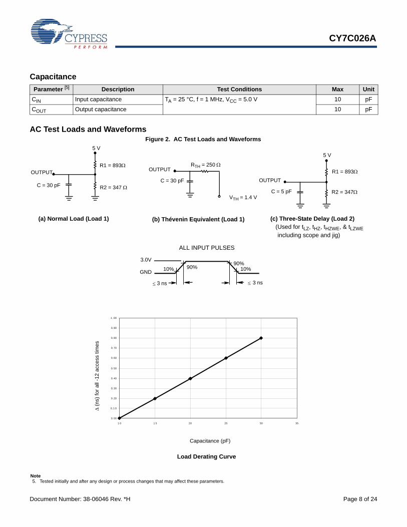
Capacitance
Parameter [5] Description Test Conditions Max Unit
CIN Input capacitance TA = 25 °C, f = 1 MHz, VCC = 5.0 V 10 pF
COUT Output capacitance 10 pF
AC Test Loads and WaveformsFigure 2. AC Test Loads and Waveforms
(a) Normal Load (Load 1)
R1 = 893
5 V
OUTPUT
R2 = 347 C = 30 pF
VTH = 1.4 V
OUTPUT
(b) Thévenin Equivalent (Load 1) (c) Three-State Delay (Load 2)
5 V
OUTPUT
RTH = 250
(Used for tLZ, tHZ, tHZWE, & tLZWE
including scope and jig)
C = 30 pF
C = 5 pF
R1 = 893
R2 = 347
3.0V
GND90%
90%10%
3 ns 3 ns
10%
ALL INPUT PULSES
0.00
0.1 0
0.20
0.30
0.40
0.50
0.60
0.70
0.80
0.90
1 .00
1 0 1 5 20 25 30 35
Load Derating Curve
Capacitance (pF)
(n
s) fo
r al
l -12
acc
ess
times
Note5. Tested initially and after any design or process changes that may affect these parameters.
CY7C026A
Document Number: 38-06046 Rev. *H Page 9 of 24
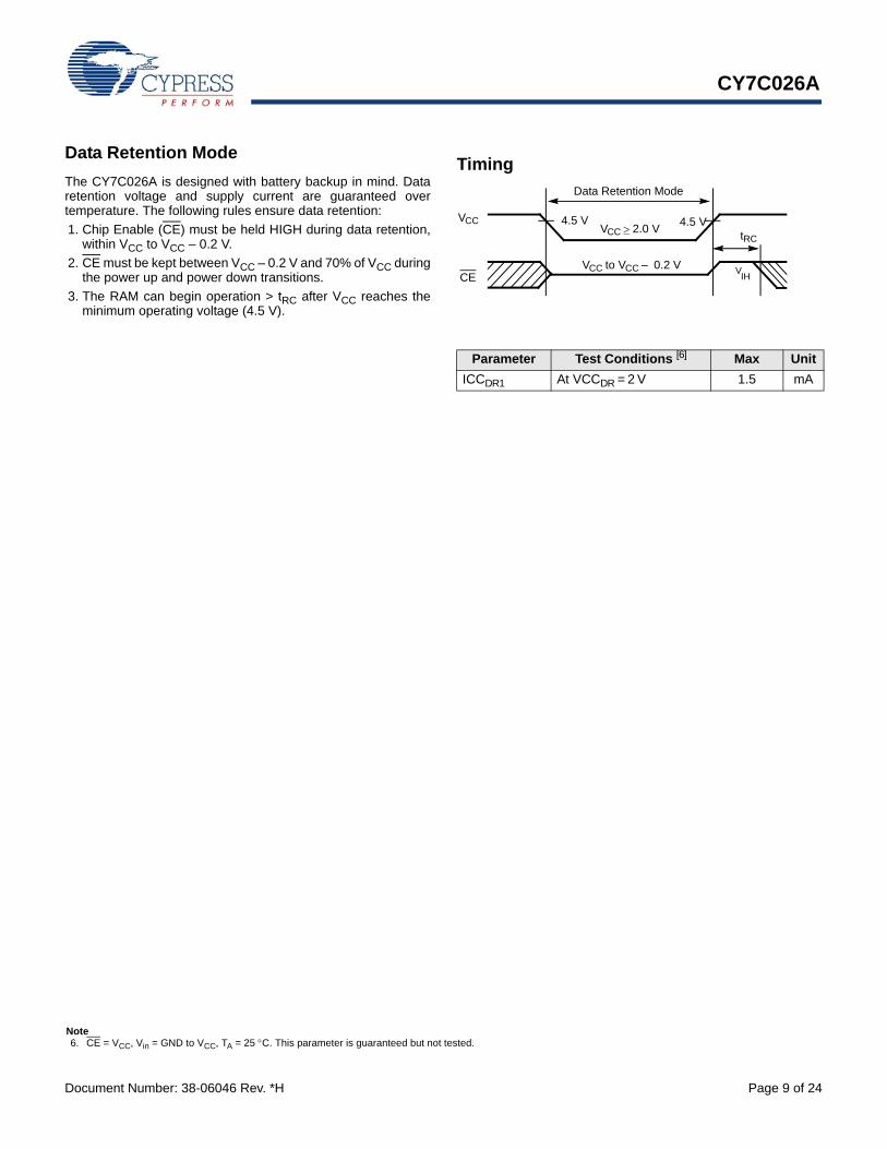
Data Retention Mode
The CY7C026A is designed with battery backup in mind. Dataretention voltage and supply current are guaranteed overtemperature. The following rules ensure data retention:
1. Chip Enable (CE) must be held HIGH during data retention,within VCC to VCC – 0.2 V.
2. CE must be kept between VCC – 0.2 V and 70% of VCC duringthe power up and power down transitions.
3. The RAM can begin operation > tRC after VCC reaches theminimum operating voltage (4.5 V).
Timing
Parameter Test Conditions [6] Max Unit
ICCDR1 At VCCDR = 2 V 1.5 mA
Data Retention Mode
4.5 V 4.5 VVCC 2.0 V
VCC to VCC – 0.2 V
VCC
CE
tRC
VIH
Note6. CE = VCC, Vin = GND to VCC, TA = 25 C. This parameter is guaranteed but not tested.
CY7C026A
Document Number: 38-06046 Rev. *H Page 10 of 24
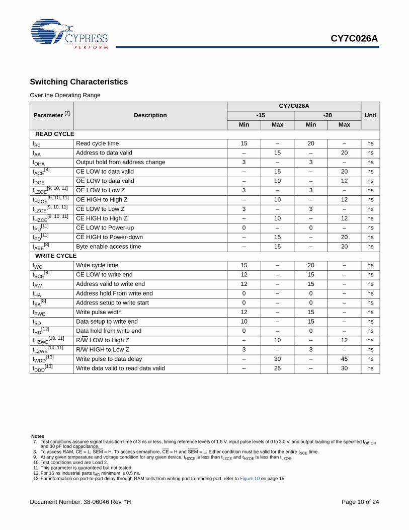
Switching Characteristics
Over the Operating Range
Parameter [7] Description
CY7C026A
Unit-15 -20
Min Max Min Max
READ CYCLE
tRC Read cycle time 15 – 20 – ns
tAA Address to data valid – 15 – 20 ns
tOHA Output hold from address change 3 – 3 – ns
tACE[8] CE LOW to data valid – 15 – 20 ns
tDOE OE LOW to data valid – 10 – 12 ns
tLZOE[9, 10, 11] OE LOW to Low Z 3 – 3 – ns
tHZOE[9, 10, 11] OE HIGH to High Z – 10 – 12 ns
tLZCE[9, 10, 11] CE LOW to Low Z 3 – 3 – ns
tHZCE[9, 10, 11] CE HIGH to High Z – 10 – 12 ns
tPU[11] CE LOW to Power-up 0 – 0 – ns
tPD[11] CE HIGH to Power-down – 15 – 20 ns
tABE[8] Byte enable access time – 15 – 20 ns
WRITE CYCLE
tWC Write cycle time 15 – 20 – ns
tSCE[8] CE LOW to write end 12 – 15 – ns
tAW Address valid to write end 12 – 15 – ns
tHA Address hold From write end 0 – 0 – ns
tSA[8] Address setup to write start 0 – 0 – ns
tPWE Write pulse width 12 – 15 – ns
tSD Data setup to write end 10 – 15 – ns
tHD[12] Data hold from write end 0 – 0 – ns
tHZWE[10, 11] R/W LOW to High Z – 10 – 12 ns
tLZWE[10, 11] R/W HIGH to Low Z 3 – 3 – ns
tWDD[13] Write pulse to data delay – 30 – 45 ns
tDDD[13] Write data valid to read data valid – 25 – 30 ns
Notes7. Test conditions assume signal transition time of 3 ns or less, timing reference levels of 1.5 V, input pulse levels of 0 to 3.0 V, and output loading of the specified IOI/IOH
and 30 pF load capacitance.8. To access RAM, CE = L, SEM = H. To access semaphore, CE = H and SEM = L. Either condition must be valid for the entire tSCE time.9. At any given temperature and voltage condition for any given device, tHZCE is less than tLZCE and tHZOE is less than tLZOE.10. Test conditions used are Load 2.11. This parameter is guaranteed but not tested.12. For 15 ns industrial parts tHD minimum is 0.5 ns.13. For information on port-to-port delay through RAM cells from writing port to reading port, refer to Figure 10 on page 15.
CY7C026A
Document Number: 38-06046 Rev. *H Page 11 of 24
BUSY TIMING[14]
tBLA BUSY LOW from address match – 15 – 20 ns
tBHA BUSY HIGH from address mismatch – 15 – 20 ns
tBLC BUSY LOW from CE LOW – 15 20 ns
tBHC BUSY HIGH from CE HIGH – 15 – 17 ns
tPS Port setup for priority 5 – 5 – ns
tWB R/W HIGH after BUSY (Slave) 0 – 0 – ns
tWH R/W HIGH after BUSY HIGH (Slave) 13 – 15 – ns
tBDD[15] BUSY HIGH to data valid – 15 – 20 ns
INTERRUPT TIMING[14]
tINS INT set time – 15 – 20 ns
tINR INT reset time – 15 – 20 ns
SEMAPHORE TIMING
tSOP SEM flag update pulse (OE or SEM) 10 – 10 – ns
tSWRD SEM flag write to read time 5 – 5 – ns
tSPS SEM flag contention window 5 – 5 – ns
tSAA SEM address access time – 15 – 20 ns
Switching Characteristics (continued)
Over the Operating Range
Parameter [7] Description
CY7C026A
Unit-15 -20
Min Max Min Max
Notes14. Test conditions used are Load 2.15. tBDD is a calculated parameter and is the greater of tWDD–tPWE (actual) or tDDD–tSD (actual).

CY7C026A
Document Number: 38-06046 Rev. *H Page 12 of 24
Switching Waveforms
Figure 3. Read Cycle No.1 (Either Port Address Access) [16, 17, 18]
Figure 4. Read Cycle No.2 (Either Port CE/OE Access) [16, 19, 20]
Figure 5. Read Cycle No. 3 (Either Port) [16, 18, 19, 20]
tRC
tAAtOHA
DATA VALIDPREVIOUS DATA VALIDDATAOUT
ADDRESS
tOHA
tACE
tLZOE
tDOE
tHZOE
tHZCE
DATA VALID
tLZCE
tPU tPD
ISB
ICC
DATAOUT
OE
CE andLB or UB
CURRENT
UB or LB
DATAOUT
tRC
ADDRESS
tAA tOHA
CE
tLZCE
tABE
tHZCE
tHZCEtACE
tLZCE
Notes16. R/W is HIGH for read cycles.17. Device is continuously selected CE = VIL and UB or LB = VIL. This waveform cannot be used for semaphore reads.18. OE = VIL.19. Address valid prior to or coincident with CE transition LOW.20. To access RAM, CE = VIL, SEM = VIH. To access semaphore, CE = VIH, SEM = VIL.
CY7C026A
Document Number: 38-06046 Rev. *H Page 13 of 24
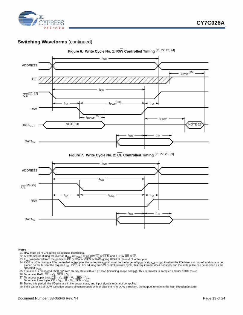
Figure 6. Write Cycle No. 1: R/W Controlled Timing [21, 22, 23, 24]
Figure 7. Write Cycle No. 2: CE Controlled Timing [21, 22, 23, 29]
Switching Waveforms (continued)
tAW
tWC
tPWE
tHDtSD
tHA
CE
R/W
OE
DATAOUT
DATAIN
ADDRESS
tHZOE
tSA
tHZWE tLZWE
[25]
[25]
[24]
[26, 27]
NOTE 28 NOTE 28
tAW
tWC
tSCE
tHDtSD
tHA
CE
R/W
DATAIN
ADDRESS
tSA
[26, 27]
Notes21. R/W must be HIGH during all address transitions.22. A write occurs during the overlap (tSCE or tPWE) of a LOW CE or SEM and a LOW UB or LB.23. tHA is measured from the earlier of CE or R/W or (SEM or R/W) going HIGH at the end of write cycle.24. If OE is LOW during a R/W controlled write cycle, the write pulse width must be the larger of tPWE or (tHZWE + tSD) to allow the I/O drivers to turn off and data to be
placed on the bus for the required tSD. If OE is HIGH during an R/W controlled write cycle, this requirement does not apply and the write pulse can be as short as the specified tPWE.
25. Transition is measured 500 mV from steady state with a 5 pF load (including scope and jig). This parameter is sampled and not 100% tested.26. To access RAM, CE = VIL, SEM = VIH.27. To access upper byte, CE = VIL, UB = VIL, SEM = VIH.
To access lower byte, CE = VIL, LB = VIL, SEM = VIH.28. During this period, the I/O pins are in the output state, and input signals must not be applied.29. If the CE or SEM LOW transition occurs simultaneously with or after the R/W LOW transition, the outputs remain in the high impedance state.
CY7C026A
Document Number: 38-06046 Rev. *H Page 14 of 24
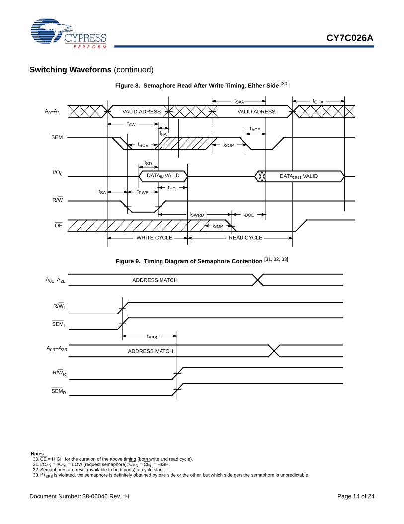
Figure 8. Semaphore Read After Write Timing, Either Side [30]
Figure 9. Timing Diagram of Semaphore Contention [31, 32, 33]
Switching Waveforms (continued)
tSOP
tSAA
VALID ADRESS VALID ADRESS
tHD
DATAIN VALID DATAOUT VALID
tOHA
tAW
tHAtACE
tSOPtSCE
tSD
tSA tPWE
tSWRD tDOE
WRITE CYCLE READ CYCLE
OE
R/W
I/O0
SEM
A0–A2
ADDRESS MATCH
tSPS
ADDRESS MATCH
R/WL
SEML
R/WR
SEMR
A0L–A2L
A0R–A2R
Notes30. CE = HIGH for the duration of the above timing (both write and read cycle).31. I/O0R = I/O0L = LOW (request semaphore); CER = CEL = HIGH.32. Semaphores are reset (available to both ports) at cycle start.33. If tSPS is violated, the semaphore is definitely obtained by one side or the other, but which side gets the semaphore is unpredictable.
CY7C026A
Document Number: 38-06046 Rev. *H Page 15 of 24
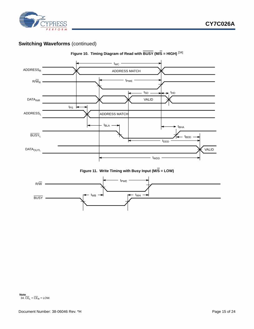
Figure 10. Timing Diagram of Read with BUSY (M/S = HIGH) [34]
Figure 11. Write Timing with Busy Input (M/S = LOW)
Switching Waveforms (continued)
VALID
tDDD
tWDD
ADDRESS MATCH
ADDRESS MATCH
R/WR
DATAINR
DATAOUTL
tWC
ADDRESSR
tPWE
VALID
tSD tHD
ADDRESSL
tPS
tBLA tBHA
tBDDBUSYL
tPWER/W
BUSYtWB tWH
Note34. CEL = CER = LOW.
CY7C026A
Document Number: 38-06046 Rev. *H Page 16 of 24
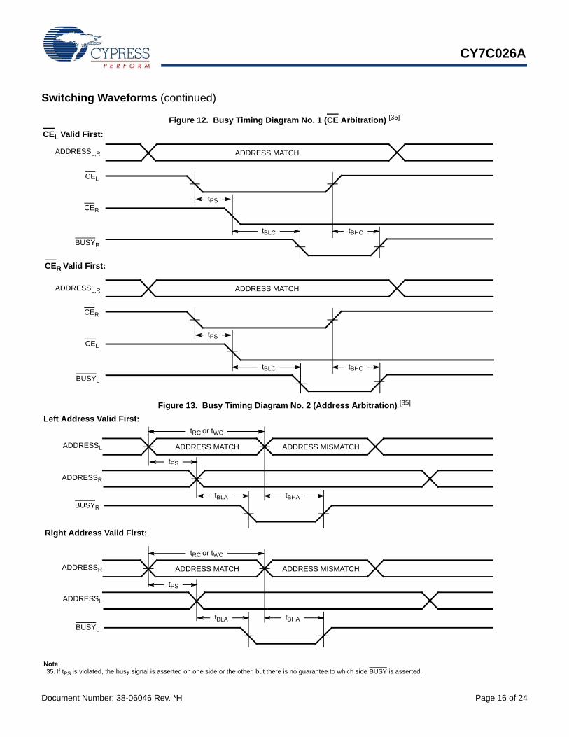
Figure 12. Busy Timing Diagram No. 1 (CE Arbitration) [35]
Figure 13. Busy Timing Diagram No. 2 (Address Arbitration) [35]
Switching Waveforms (continued)
ADDRESS MATCH
tPS
tBLC tBHC
ADDRESS MATCH
tPS
tBLC tBHC
CER Valid First:
ADDRESSL,R
BUSYR
CEL
CER
BUSYL
CER
CEL
ADDRESSL,R
CEL Valid First:
ADDRESS MATCH
tPS
ADDRESSL
BUSYR
ADDRESS MISMATCH
tRC or tWC
tBLA tBHA
ADDRESSR
ADDRESS MATCH ADDRESS MISMATCH
tPS
ADDRESSL
BUSYL
tRC or tWC
tBLA tBHA
ADDRESSR
Right Address Valid First:
Left Address Valid First:
Note35. If tPS is violated, the busy signal is asserted on one side or the other, but there is no guarantee to which side BUSY is asserted.
CY7C026A
Document Number: 38-06046 Rev. *H Page 17 of 24
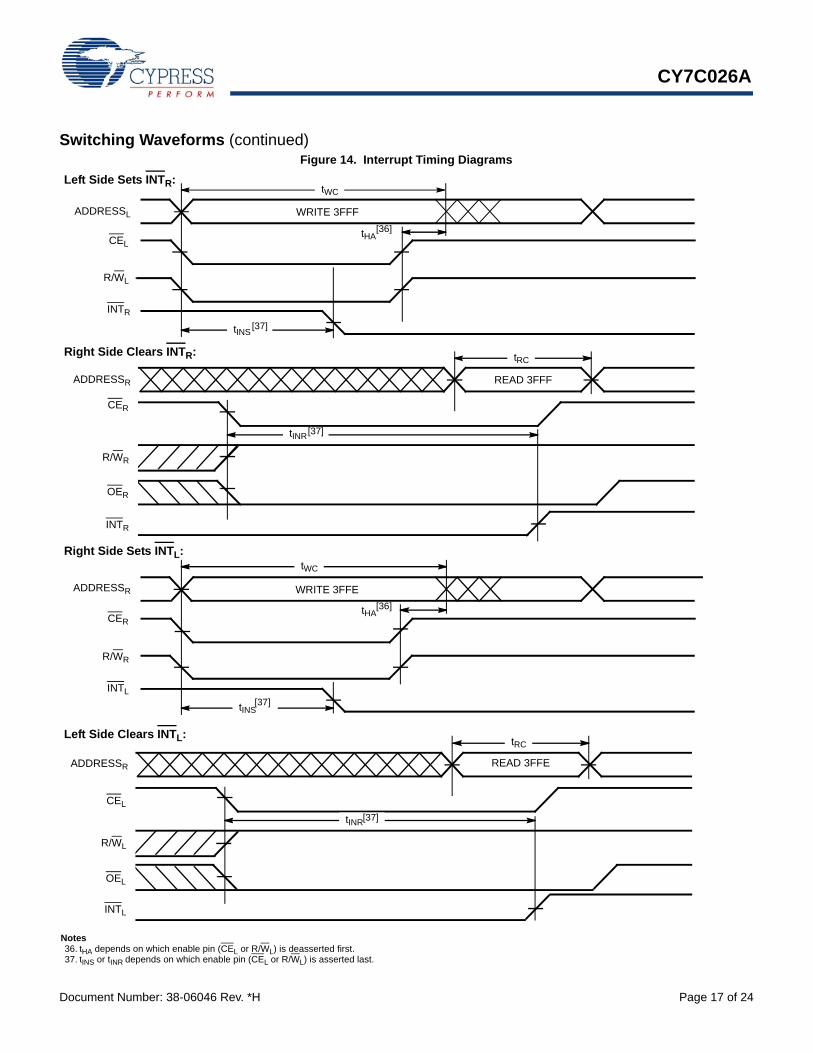
Figure 14. Interrupt Timing Diagrams
Switching Waveforms (continued)
WRITE 3FFF
tWC
Right Side Clears INTR:
tHA
READ 3FFF
tRC
tINR
WRITE 3FFE
tWC
Right Side Sets INTL:
Left Side Sets INTR:
Left Side Clears INTL:
READ 3FFE
tINR
tRC
ADDRESSR
CEL
R/WL
INTL
OEL
ADDRESSR
R/WR
CER
INTL
ADDRESSR
CER
R/WR
INTR
OER
ADDRESSL
R/WL
CEL
INTR
tINS
tHA
tINS
[36]
[37]
[37]
[37]
[36]
[37]
Notes36. tHA depends on which enable pin (CEL or R/WL) is deasserted first.37. tINS or tINR depends on which enable pin (CEL or R/WL) is asserted last.
CY7C026A
Document Number: 38-06046 Rev. *H Page 18 of 24
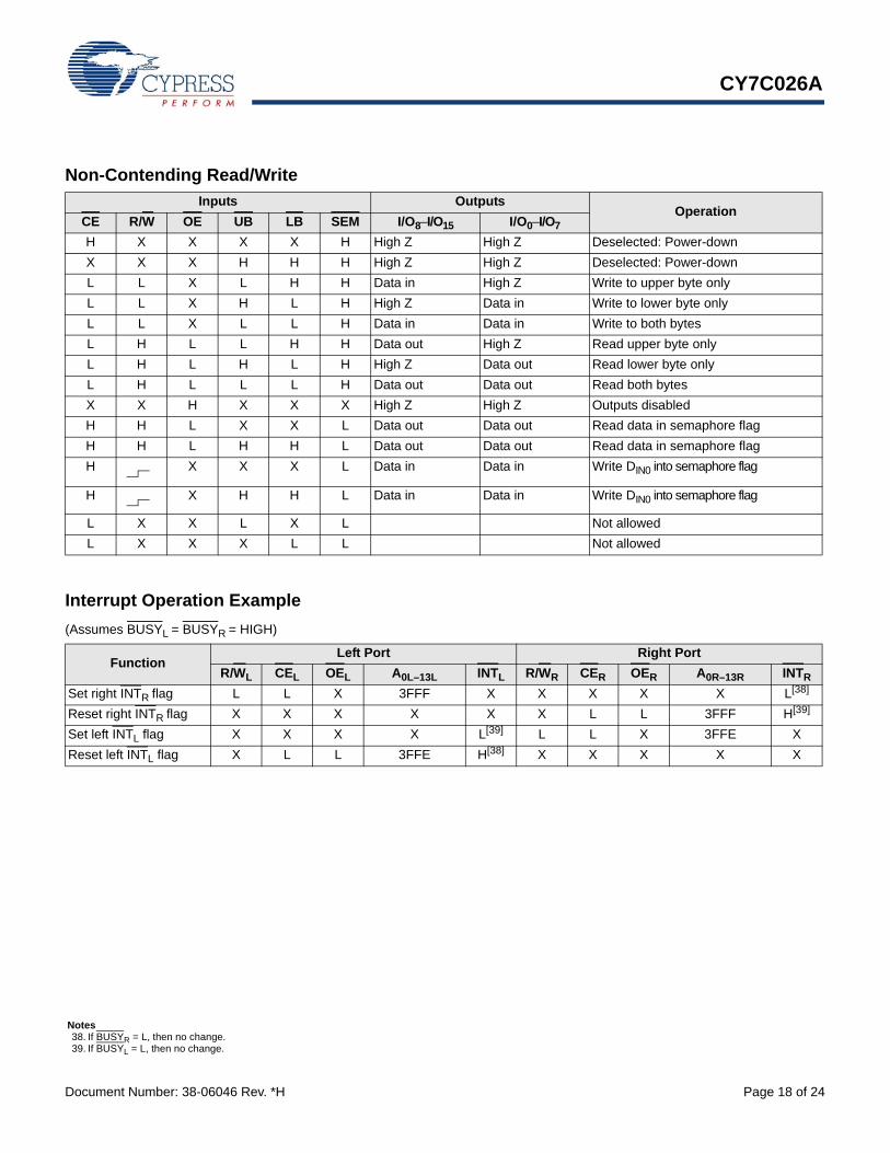
Non-Contending Read/Write
Inputs OutputsOperation
CE R/W OE UB LB SEM I/O8–I/O15 I/O0–I/O7
H X X X X H High Z High Z Deselected: Power-down
X X X H H H High Z High Z Deselected: Power-down
L L X L H H Data in High Z Write to upper byte only
L L X H L H High Z Data in Write to lower byte only
L L X L L H Data in Data in Write to both bytes
L H L L H H Data out High Z Read upper byte only
L H L H L H High Z Data out Read lower byte only
L H L L L H Data out Data out Read both bytes
X X H X X X High Z High Z Outputs disabled
H H L X X L Data out Data out Read data in semaphore flag
H H L H H L Data out Data out Read data in semaphore flag
H X X X L Data in Data in Write DIN0 into semaphore flag
H X H H L Data in Data in Write DIN0 into semaphore flag
L X X L X L Not allowed
L X X X L L Not allowed
Interrupt Operation Example
(Assumes BUSYL = BUSYR = HIGH)
FunctionLeft Port Right Port
R/WL CEL OEL A0L–13L INTL R/WR CER OER A0R–13R INTR
Set right INTR flag L L X 3FFF X X X X X L[38]
Reset right INTR flag X X X X X X L L 3FFF H[39]
Set left INTL flag X X X X L[39] L L X 3FFE X
Reset left INTL flag X L L 3FFE H[38] X X X X X
Notes38. If BUSYR = L, then no change.39. If BUSYL = L, then no change.
CY7C026A
Document Number: 38-06046 Rev. *H Page 19 of 24
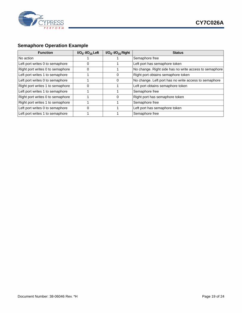
Semaphore Operation Example
Function I/O0–I/O15 Left I/O0–I/O15 Right Status
No action 1 1 Semaphore free
Left port writes 0 to semaphore 0 1 Left port has semaphore token
Right port writes 0 to semaphore 0 1 No change. Right side has no write access to semaphore
Left port writes 1 to semaphore 1 0 Right port obtains semaphore token
Left port writes 0 to semaphore 1 0 No change. Left port has no write access to semaphore
Right port writes 1 to semaphore 0 1 Left port obtains semaphore token
Left port writes 1 to semaphore 1 1 Semaphore free
Right port writes 0 to semaphore 1 0 Right port has semaphore token
Right port writes 1 to semaphore 1 1 Semaphore free
Left port writes 0 to semaphore 0 1 Left port has semaphore token
Left port writes 1 to semaphore 1 1 Semaphore free
CY7C026A
Document Number: 38-06046 Rev. *H Page 20 of 24
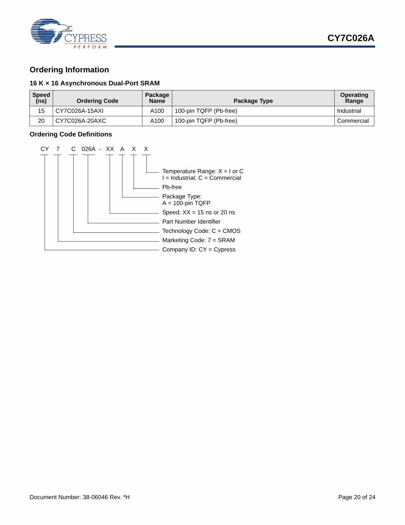
Ordering Information
Ordering Code Definitions
16 K × 16 Asynchronous Dual-Port SRAM
Speed(ns) Ordering Code
PackageName Package Type
OperatingRange
15 CY7C026A-15AXI A100 100-pin TQFP (Pb-free) Industrial
20 CY7C026A-20AXC A100 100-pin TQFP (Pb-free) Commercial
Temperature Range: X = I or C I = Industrial; C = Commercial
Pb-free
Package Type: A = 100-pin TQFP
Speed: XX = 15 ns or 20 ns
Part Number Identifier
Technology Code: C = CMOS
Marketing Code: 7 = SRAM
Company ID: CY = Cypress
026AC - XX A XCY 7 X
CY7C026A
Document Number: 38-06046 Rev. *H Page 21 of 24
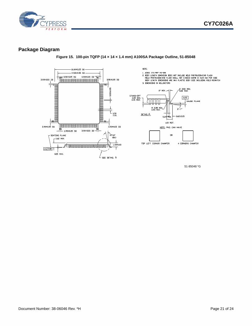
Package Diagram
Figure 15. 100-pin TQFP (14 × 14 × 1.4 mm) A100SA Package Outline, 51-85048
51-85048 *G
CY7C026A
Document Number: 38-06046 Rev. *H Page 22 of 24
Acronyms Document Conventions
Units of MeasureAcronym Description
CMOS complementary metal oxide semiconductor
I/O input/output
SRAM static random access memory
TQFP thin quad plastic flatpack
Symbol Unit of Measure
°C degree Celsius
MHz megahertz
µA microampere
mA milliampere
mV millivolt
ns nanosecond
ohm
pF picofarad
V volt
W watt
CY7C026A
Document Number: 38-06046 Rev. *H Page 23 of 24
Document History Page
Document Title: CY7C026A, 16 K × 16 Dual-Port Static RAMDocument Number: 38-06046
Rev. ECN No. Orig. of Change
Submission Date Description of Change
** 110198 SZV 09/29/01 Change from Spec number: 38-00832 to 38-06046
*A 122296 RBI 12/27/02 Power up requirements added to Maximum Ratings Information
*B 237621 YDT See ECN Removed cross information from features section
*C 393454 YIM See ECN Added Pb-free LogoAdded Pb-free parts to ordering information:CY7C026A-15AXC, CY7C026A-20AXC
*D 2623540 VKN / PYRS
12/17/08 Added CY7C026B partAdded CY7C026A-15AXI part in the Ordering Information table
*E 2896038 RAME 03/19/10 Removed inactive parts from ordering information tableUpdated package diagram
*F 3081925 ADMU 11/10/2010 Changed title from CY7C026A/026B, CY7C036A 16K X 16/18 DUAL-PORT STATIC RAM to CY7C026A 16K X 16 DUAL-PORT STATIC RAMRemoved all information on CY7C026B and CY7C036ARemoved information on speed bin 12.Added Acronyms and Units of Measure table.Added Ordering Code Definition.Updated as per new template
*G 3403652 ADMU 10/14/2011 Removed pruned part CY7C026A-20AC from Ordering InformationUpdated Package Diagram.
*H 3799343 SMCH 10/31/2012 Updated Logic Block Diagram (No change in diagram, removed the notes “I/O8–I/O15 for × 16 devices.” and “I/O0–I/O7 for × 16 devices.” and their references in Logic Block Diagram).Updated Switching Characteristics (Updated Note 8 (Removed “UB = L”)).Updated Switching Waveforms (Updated Note 20 (Removed “UB or LB = VIL”), updated Figure 9 (Replaced “MATCH” with “ADDRESS MATCH”), updated Figure 10 (Replaced “MATCH” with “ADDRESS MATCH”)).Updated Non-Contending Read/Write (Replaced “X” with “H” for CE inputs of “Read data in semaphore flag” and “Write DIN0 into semaphore flag” operations).Updated Package Diagram (spec 51-85048 (Changed revision from *E to *G)).
Document Number: 38-06046 Rev. *H Revised October 31, 2012 Page 24 of 24
All products and company names mentioned in this document may be the trademarks of their respective holders.
CY7C026A
© Cypress Semiconductor Corporation, 2009-2012. The information contained herein is subject to change without notice. Cypress Semiconductor Corporation assumes no responsibility for the use ofany circuitry other than circuitry embodied in a Cypress product. Nor does it convey or imply any license under patent or other rights. Cypress products are not warranted nor intended to be used formedical, life support, life saving, critical control or safety applications, unless pursuant to an express written agreement with Cypress. Furthermore, Cypress does not authorize its products for use ascritical components in life-support systems where a malfunction or failure may reasonably be expected to result in significant injury to the user. The inclusion of Cypress products in life-support systemsapplication implies that the manufacturer assumes all risk of such use and in doing so indemnifies Cypress against all charges.
Any Source Code (software and/or firmware) is owned by Cypress Semiconductor Corporation (Cypress) and is protected by and subject to worldwide patent protection (United States and foreign),United States copyright laws and international treaty provisions. Cypress hereby grants to licensee a personal, non-exclusive, non-transferable license to copy, use, modify, create derivative works of,and compile the Cypress Source Code and derivative works for the sole purpose of creating custom software and or firmware in support of licensee product to be used only in conjunction with a Cypressintegrated circuit as specified in the applicable agreement. Any reproduction, modification, translation, compilation, or representation of this Source Code except as specified above is prohibited withoutthe express written permission of Cypress.
Disclaimer: CYPRESS MAKES NO WARRANTY OF ANY KIND, EXPRESS OR IMPLIED, WITH REGARD TO THIS MATERIAL, INCLUDING, BUT NOT LIMITED TO, THE IMPLIED WARRANTIESOF MERCHANTABILITY AND FITNESS FOR A PARTICULAR PURPOSE. Cypress reserves the right to make changes without further notice to the materials described herein. Cypress does notassume any liability arising out of the application or use of any product or circuit described herein. Cypress does not authorize its products for use as critical components in life-support systems wherea malfunction or failure may reasonably be expected to result in significant injury to the user. The inclusion of Cypress’ product in a life-support systems application implies that the manufacturerassumes all risk of such use and in doing so indemnifies Cypress against all charges.
Use may be limited by and subject to the applicable Cypress software license agreement.
Sales, Solutions, and Legal Information
Worldwide Sales and Design Support
Cypress maintains a worldwide network of offices, solution centers, manufacturer’s representatives, and distributors. To find the office closest to you, visit us at cypress.com/sales.
Products
Automotive cypress.com/go/automotive
Clocks & Buffers cypress.com/go/clocks
Interface cypress.com/go/interface
Lighting & Power Control cypress.com/go/powerpsoc
cypress.com/go/plc
Memory cypress.com/go/memory
Optical & Image Sensing cypress.com/go/image
PSoC cypress.com/go/psoc
Touch Sensing cypress.com/go/touch
USB Controllers cypress.com/go/USB
Wireless/RF cypress.com/go/wireless
PSoC Solutions
psoc.cypress.com/solutions
PSoC 1 | PSoC 3 | PSoC 5