cxa1372bq/bs - jos van dijken · focus servo is switched through fs3 on and off. flb i ... – 7...
TRANSCRIPT

Description
The CXA1372BQ/BS is a bipolar IC developed for
RF signal processing (focus OK, mirror, defect
detection, EFM comparator) and various servo
control.
Features
• Dual ±5V and single 5V power supplies
• Low power consumption
• Fewer external parts
• Disc defect countermeasure circuit
• Fully compatible with the CXA1182 for microcomputer
software
Functions
• Auto asymmetry control
• Focus OK detection circuit
• Mirror detection circuit
• Defect detection, countermeasure circuit
• EFM comparator
• Focus servo control
• Tracking servo control
• Sled servo control
Structure
Bipolar silicon monolithic IC
Absolute Maximum Ratings (Ta = 25°C)
• Supply voltage VCC – VEE 12 V
• Operating temperature
Topr –20 to +75 °C
• Storage temperature
Tstg –65 to +150 °C
• Allowable power dissipation
PD 457 (CXA1372BQ) mW
833 (CXA1372BS) mW
Recommended Operating Conditions
VCC – VEE 3.6 to 11 V
VCC – DGND 3.6 to 5.5 V
– 1 –
CXA1372BQ/BS
E95927A67-PS
RF Signal Processing Servo Amplifier for CD Player
Sony reserves the right to change products and specifications without prior notice. This information does not convey any license byany implication or otherwise under any patents or other right. Application circuits shown, if any, are typical examples illustrating theoperation of the devices. Sony cannot assume responsibility for any problems arising out of the use of these circuits.
CXA1372BQ
48 pin QFP (Plastic)
CXA1372BS
48 pin SDIP (Plastic)

– 2 –
CXA1372BQ/BS
Block Diagram
35 34 30313233 2526272829
• IIL↓
• TTL
20
21
22
23
24
19
13
14
15
16
17
18
• I SET
• F SETTM6
TM5
TM4
TM3
TM7
121110987654321
FS3 FS2
FS1
• FOCUS PHASE COMPENSATION
48
47
46
45
44
43
42
41
40
39
37
DFCT
• BPF • WINDOW COMPARATOR
DFCTTG1 • TRACKING
PHASE COMPENSATION
• IIL DATA REGISTER
• OUTPUT DECODER
• INPUT SHIFT REGISTER• ADDRESS DECODER
• FS1 to 4 • TG1 to 2 • TM1 to 7 • PS1 to 3
• TTL↓
• IIL
DV
cc
CC
2
CC
1
FO
K
EF
M
AS
Y
DF
CT
MIR
R
DG
ND
SE
NS
C. O
UT
XR
ST
DATA
XLT
CLK
LOCK
DIRC
AVEE
SSTOP
ISET
FSET
SL–
SLO
SL+
TA
–
TA
O
AV
CC
TG
2
TG
U
SR
CH
FE
–
FE
O
FLB
FS
3
FG
D
VC
FDFCT
FE
FZC
ATSC
TDFCT
TE
TZC
DVEE
RFO
RFI
CP
CB
36
TM1
FS4
TG2
TM2
• TTL↓
• IIL
38
– 3 –
CXA1372BQ/BS
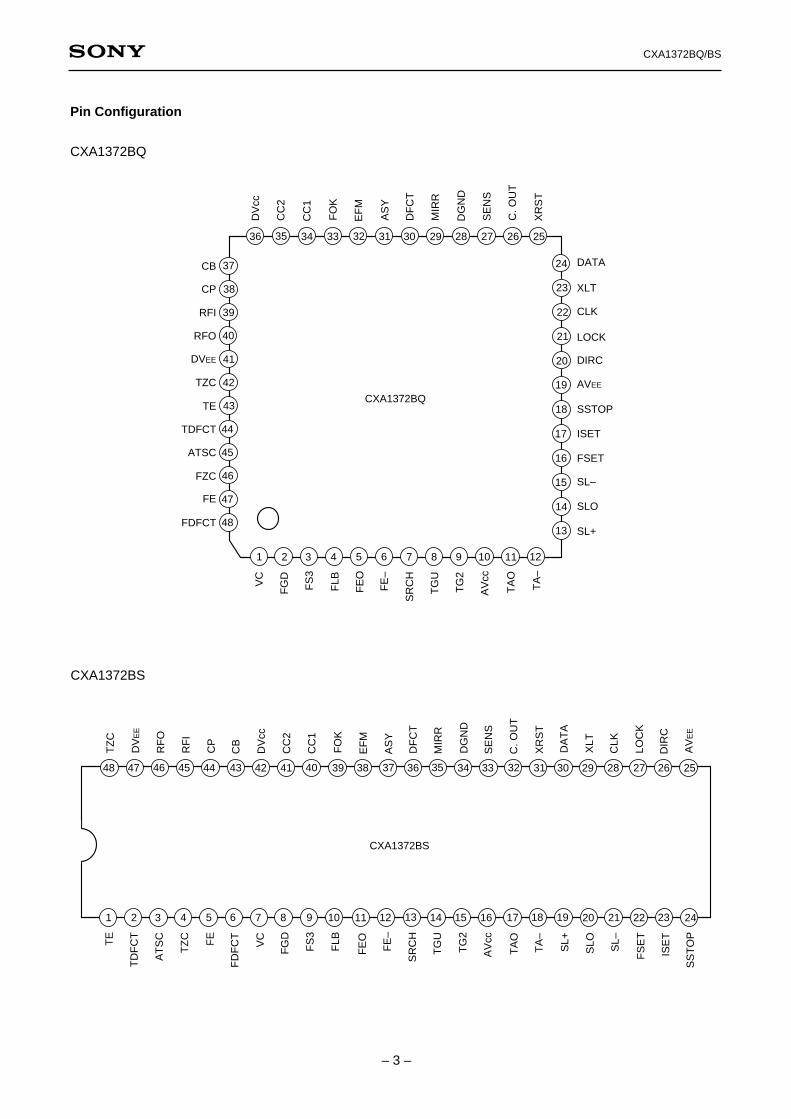
Pin Configuration
CXA1372BQ
2 3 4 5 6 7 8 9 10 11 12
13
14
15
16
17
18
19
20
21
22
23
24
252627282930
40
39
38
37
36 35 34 313233
41
42
43
44
45
46
47
48
1
CB
CP
RFI
RFO
DVEE
TZC
TE
TDFCT
ATSC
FZC
FE
FDFCT
DATA
XLT
CLK
LOCK
DIRC
AVEE
SSTOP
ISET
FSET
SL–
SLO
SL+
VC
FG
D
FS
3
FLB
FE
O
FE
–
SR
CH
TG
U
TG
2
AV
cc
TA
O
TA
–
DV
cc
CC
2
CC
1
FO
K
EF
M
AS
Y
DF
CT
MIR
R
DG
ND
SE
NS
C. O
UT
XR
ST
CXA1372BQ
CXA1372BS
2 3 4 5 6 7 8 9 10 11 12 13 14 15 16 17 18 19 20 21 22 23 24
25262728293040 39 38 37 36 35 34 3132334142434445464748
1
TE
TD
FC
T
AT
SC
TZ
C FE
FD
FC
T
VC
FG
D
FS
3
FLB
FE
O
FE
–
SR
CH
TG
U
TG
2
AV
cc
TA
O
TA
–
SL+
SLO SL–
FS
ET
ISE
T
SS
TO
P
TZ
C
DV
EE
RF
O
RF
I
CP
CB
DV
cc
CC
2
CC
1
FO
K
EF
M
AS
Y
DF
CT
MIR
R
DG
ND
SE
NS
C. O
UT
XR
ST
DA
TA
XLT
CLK
LOC
K
DIR
C
AV
EE
CXA1372BS

– 4 –
CXA1372BQ/BS
Pin Description
Pin No.Symbol I/O Equivalent circuit Description
VC I
Center voltage input.For dual power supplies: GNDFor single power supply:
(VCC + GND)/2
FGD IConnects a capacitor between thispin and Pin 3 to cut high-frequencygain.
FS3 IThe high-frequency gain of thefocus servo is switched through FS3ON and OFF.
FLB IExternal time constant to boost thelow frequency of the focus servo.
FEO O
TAO O
SLO O
Focus drive output.
Tracking drive output.
Sled drive output.
1
2
3
4
5
11
14
6
7
8
9
10
11
17
20
12 FE– I Inverted input for focus amplifier.147
40k
90k
2.5µA
6
5
11
14 250µA
2.5µA
40k4
2
Vcc
VEE
147 48k
130k 20µA
346k 580k
Q S
– 5 –
CXA1372BQ/BS
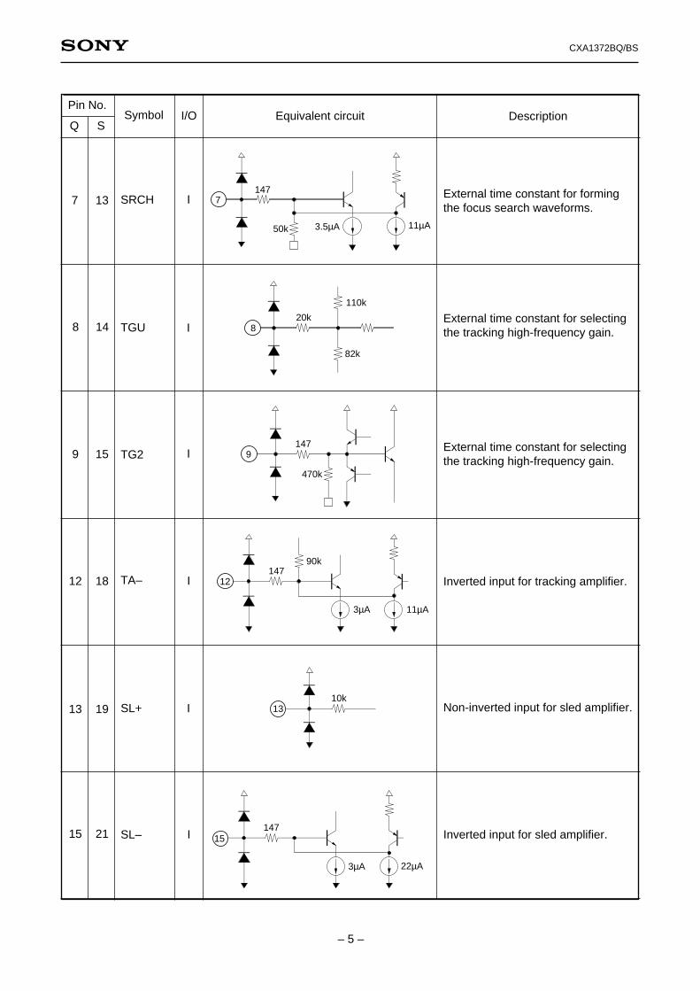
External time constant for formingthe focus search waveforms.
External time constant for selectingthe tracking high-frequency gain.
External time constant for selectingthe tracking high-frequency gain.
Inverted input for tracking amplifier.
Non-inverted input for sled amplifier.
Inverted input for sled amplifier.
Pin No.Symbol I/O Equivalent circuit Description
SRCH I
TGU I
TG2 I
TA– I
SL+ I
13
14
15
18
19
21
7
8
9
12
13
15 SL– I147
22µA3µA
15
10k13
14790k
11µA3µA
12
147
50k 11µA3.5µA
7
20k
110k
82k
8
470k
1479
Q S
– 6 –
CXA1372BQ/BS
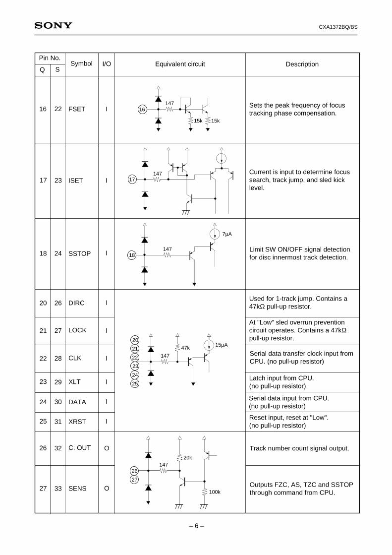
Serial data transfer clock input fromCPU. (no pull-up resistor)
Serial data input from CPU.(no pull-up resistor)
Reset input, reset at "Low".(no pull-up resistor)
Latch input from CPU.(no pull-up resistor)
Track number count signal output.
Outputs FZC, AS, TZC and SSTOPthrough command from CPU.
Sets the peak frequency of focustracking phase compensation.
Current is input to determine focussearch, track jump, and sled kicklevel.
Used for 1-track jump. Contains a47kΩ pull-up resistor.
At "Low" sled overrun preventioncircuit operates. Contains a 47kΩpull-up resistor.
Limit SW ON/OFF signal detectionfor disc innermost track detection.
Pin No.Symbol I/O Equivalent circuit Description
FSET I
ISET I
SSTOP I
DIRC I
LOCK I
22
23
24
26
27
33
16
17
18
20
21
CLK I2822
XLT I2923
DATA I3024
XRST I3125
27 SENS O
3226 C. OUT O
100k
14720k
26
27
147
47k 15µA20
21
22
23
24
25
147
15k 15k
16
14717
147
7µA
18
Q S

– 7 –
CXA1372BQ/BS
Input for DEFECT bottom holdoutput with capacitance coupled.
Pin No.Symbol I/O Equivalent circuit Description
29 MIRR O
38 CP I
MIRR comparator output.(DC voltage: 10kΩ load connected)
Connects MIRR hold capacitor.Non-inverted input for MIRRcomparator.
34 CC1 O
35 CC2 I
30 DFCT O
37 CB I
31 ASY I Auto asymmetry control input.
32 EFM O EFM comparator output.(DC voltage: 10kΩ load connected)
33
35
44
40
41
36
43
37
38
39 FOK OFOK comparator output.(DC voltage: 10kΩ load connected)
14733
20k
4.8k
Current source depending on power supply(VCC to DGND)
32
14731
147
147
20k29
38
14737
14735
14734
14730
DEFECT bottom hold output.
Connects DEFECT bottom holdcapacitor.
DEFECT comparator output.(DC voltage: 10kΩ load connected)
Q S

– 8 –
CXA1372BQ/BS
Input for RF summing amplifieroutput with capacitance coupled.
Tracking zero-cross comparatorinput.
Connects a capacitor for timeconstant during defect.
Tracking error input.
Window comparator input for ATSCdetection.
Focus zero-cross comparator input.
Focus error input.
Connects a capacitor for timeconstant during defect.
Pin No.Symbol I/O Equivalent circuit Description
RFI I
TZC I
TE I
ATSC I
FZC I
45
48
1
3
4
5
39
RF summing amplifier output.Check point of eye pattern.
RFO O4640
42
43
TDFCT I244
45
46
47 FE I
648 FDFCT I
147
147
470k47
48
14746
1.2k
60k
330k
45
Vcc
VEE
470k
47P
14739
40147
40k
42147
75k
7µA
147
147
43
44
470k
Q S
– 9 –
CXA1372BQ/BS
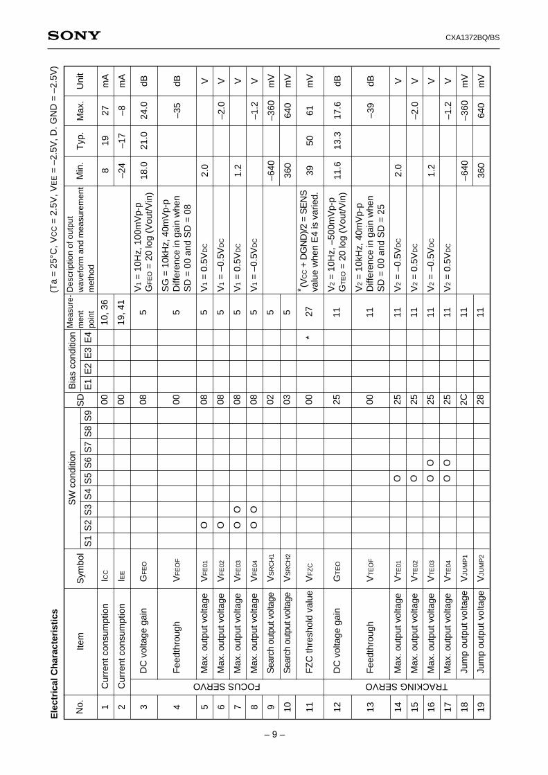
Ele
ctri
cal C
har
acte
rist
ics
(Ta
= 2
5°C
, VC
C=
2.5
V, V
EE
= –
2.5V
, D. G
ND
= –
2.5V
)
No.
Cur
rent
con
sum
ptio
n
Cur
rent
con
sum
ptio
n
O O OO
OO
S1
S2
S3
S4
S5
S6
S7
S8
S9
E1
E2
E3
E4
SD
Mea
sure
-m
ent
poin
t
Des
crip
tion
of o
utpu
tw
avef
orm
and
mea
sure
men
tm
etho
d
10, 3
6
19, 4
1
5 5 5 5 5 5 5 5 27 11 11 11 11 11 11 11 11
Uni
tM
ax.
Typ
.M
in.
Item
Sym
bol
Bia
s co
nditi
onS
W c
ondi
tion
1 2 3 4 5 6 7 8 9 10 11 12 13 14 15 16 17 18 19
DC
vol
tage
gai
n
Fee
dthr
ough
Max
. out
put v
olta
ge
Max
. out
put v
olta
ge
Max
. out
put v
olta
ge
Max
. out
put v
olta
ge
Sea
rch
outp
ut v
olta
ge
Sea
rch
outp
ut v
olta
ge
FZ
C th
resh
old
valu
e
DC
vol
tage
gai
n
Fee
dthr
ough
Max
. out
put v
olta
ge
Max
. out
put v
olta
ge
Max
. out
put v
olta
ge
Max
. out
put v
olta
ge
Jum
p ou
tput
vol
tage
Jum
p ou
tput
vol
tage
I CC
IEE
GF
EO
VF
EO
F
VF
E01
VF
E02
VF
E03
VF
E04
VS
RC
H1
VS
RC
H2
VF
ZC
GT
EO
VT
EO
F
VT
E01
VT
E02
VT
E03
VT
E04
VJU
MP
1
VJU
MP
2
O O OO
OO
00 00 08 00 08 08 08 08 02 03 00 25 00 25 25 25 25 2C 28
8 –24
18.0
2.0
1.2
–640
360
39 11.6
2.0
1.2
–640
360
19 –17
21.0
50 13.3
27 –8 24.0
–35
–2.0
–1.2
–360
640
61 17.6
–39
–2.0
–1.2
–360
640
mA
mA
dB dB V V V V mV
mV
mV
dB dB V V V V mV
mV
V1
= 1
0Hz,
100
mV
p-p
GF
EO
= 2
0 lo
g (V
out/V
in)
SG
= 1
0kH
z, 4
0mV
p-p
Diff
eren
ce in
gai
n w
hen
SD
= 0
0 an
d S
D =
08
V1
= 0
.5V
DC
V1
= –
0.5V
DC
V1
= 0
.5V
DC
V1
= –
0.5V
DC
∗ (V
CC
+ D
GN
D)/2
= S
EN
Sva
lue
whe
n E
4 is
var
ied.
V2
= 1
0Hz,
–50
0mV
p-p
GT
EO
= 2
0 lo
g (V
out/V
in)
V2
= 1
0kH
z, 4
0mV
p-p
Diff
eren
ce in
gai
n w
hen
SD
= 0
0 an
d S
D =
25
V2
= –
0.5V
DC
V2
= 0
.5V
DC
V2
= –
0.5V
DC
V2
= 0
.5V
DC
FOCUS SERVO TRACKING SERVO
∗

– 10 –
CXA1372BQ/BS
No.
O O
S1
S2
S3
S4
S5
S6
S7
S8
S9
E1
E2
E3
E4
SD
Mea
sure
-m
ent
poin
t
Des
crip
tion
of o
utpu
tw
avef
orm
and
mea
sure
men
tm
etho
d
27 27 27 14 14 14 14 14 14 14 14 27 27 26 33 33 33 33
Uni
tM
ax.
Typ
.M
in.
Sym
bol
Bia
s co
nditi
onS
W c
ondi
tion
20 21 22 23 24 25 26 27 28 29 30 31 32 33 34 35 36 37
10 10 20 25 00 25 25 25 25 23 22 30
–45 7 –20
50 2.0
2.0
–750
450
–40
–400
2.2
45
–26
26 0 –25
–356
–7 45 20 –34
–2.0
–2.0
–450
750
–10
–2.0
–2.0
–330
–1.8
mV
mV
mV
dB dB V V V V mV
mV
mV V V mV V V kHz
∗ (V
CC
+ D
GN
D)/2
= S
EN
Sva
lue
whe
n E
3 is
var
ied.
∗ (V
CC
+ D
GN
D)/2
= S
EN
Sva
lue
whe
n E
2 is
var
ied.
V5
= 1
0Hz,
20m
Vp-
pO
pen
loop
gai
n
V5
= 1
0kH
z, 1
00m
Vp-
pD
iffer
ence
in g
ain
whe
nS
D =
00
and
SD
= 2
5
V5
= 1
.0V
DC
V5
= –
1.0V
DC
V5
= 1
.0V
DC
V5
= –
1.0V
DC
∗ (V
CC
+ D
GN
D)/2
= S
EN
Sva
lue
whe
n E
1 is
var
ied.
(VC
C+
DG
ND
)/2
= v
alue
betw
een
Pin
s 39
and
40
whe
n V
4is
var
ied.
V4
= 1
Vp-
p –
375m
VD
C
FOKA
TS
C th
resh
old
valu
e
AT
SC
thre
shol
d va
lue
TZ
C th
resh
old
valu
e
DC
vol
tage
gai
n
Fee
dthr
ough
Max
. out
put v
olta
ge
Max
. out
put v
olta
ge
Max
. out
put v
olta
ge
Max
. out
put v
olta
ge
Kic
k ou
tput
vol
tage
Kic
k ou
tput
vol
tage
SS
TO
P th
resh
old
valu
e
SE
NS
Low
leve
l
CO
UT
Low
leve
l
FO
K th
resh
old
valu
e
Hig
h le
vel v
olta
ge
Low
leve
l vol
tage
Max
. ope
ratin
g fre
quen
cy
VA
TS
C1
VA
TS
C2
VT
ZC
GS
LO
VS
LOF
VS
L01
VS
L02
VS
L03
VS
L04
VK
ICK
1
VK
ICK
2
VS
ST
OP
VS
EN
S
VC
OU
T
VF
OK
T
VF
OK
H
VF
OK
L
FF
OK
SLED SERVOTRACKINGSERVO
∗
∗
∗
Item
– 11 –
CXA1372BQ/BS
S1
S2
S3
S4
S5
S6
S7
S8
S9
E1
E2
E3
E4
SD
Mea
sure
-m
ent
poin
t
Des
crip
tion
of o
utpu
tw
avef
orm
and
mea
sure
men
tm
etho
d
29 29 29 29 29 30 30 30 30 30 30 31 31 32 32 A A
Uni
tM
ax.
Typ
.M
in.
Sym
bol
Bia
s co
nditi
onS
W c
ondi
tion
38 39 40 41 42 43 44 45 46 47 48 49 50 51 52 53 54
Hig
h le
vel v
olta
ge
Low
leve
l vol
tage
Max
. ope
ratin
g fr
eque
ncy
Min
. inp
ut o
pera
ting
volta
ge
Max
. inp
ut o
pera
ting
volta
ge
Hig
h le
vel o
utpu
t vo
ltage
Low
leve
l out
put
volta
ge
Min
. ope
ratin
g fr
eque
ncy
Max
. ope
ratin
g fr
eque
ncy
Min
. inp
ut o
pera
ting
volta
ge
Max
. inp
ut o
pera
ting
volta
ge
Dut
y 1
Dut
y 2
Hig
h le
vel o
utpu
t vo
ltage
Low
leve
l out
put
volta
ge
Min
. inp
ut o
pera
ting
volta
ge
Max
. inp
ut o
pera
ting
volta
ge
VM
IRH
VM
IRL
FM
IR
VM
IR1
VM
IR2
VD
FC
TH
VD
FC
TL
FD
FC
T1
FD
FC
T2
VD
FC
T1
VD
FC
T2
DE
FM
1
DE
FM
2
VE
FM
H
VE
FM
L
VE
FM
1
VE
FM
2
O O O
O
O
O
1.8
30 1.8
1.8
2.5
1.8
–50 0 1.2
1.8
0 50
–2.0
0.3
–2.0 1 0.5
50 100
–1.2
0.12
V V kHz
Vp-
p
Vp-
p
V V kHz
kHz
Vp-
p
Vp-
p
mV
mV V V
Vp-
p
Vp-
p
V4
= 1
0kH
z1.
0Vp-
p –
0.4V
DC
V4
= 8
00m
Vp-
p –
0.4V
DC
V4
= 1
0kH
z –
0.4V
DC
V4
= 0
.8V
p-p
+ 3
75m
VD
C
V4
= 5
0Hz
+ 3
75m
VD
C
(squ
are
wav
e)
V4
= 7
50kH
z, 0
.7V
p-p
V4
= 7
50kH
z,0.
7Vp-
p +
0.2
5VD
C
V4
= 7
50kH
z, 0
.7V
p-p
V4
= 7
50kH
z
DEFECT EFMMIRROR
Item
No.
O O

– 12 –
CXA1372BQ/BS
Electric Characteristics Measurement Circuit
GND
0.1µ
S1
GND
1000
P
130
13k
S3
100k
200kS2 S4
0.033µ
AVcc
GND
130
S6
100k
200kS5
GND
13k
GND
V5
AC
130
13kS7
60k
5.1k
GN
D
510k Vcc
240k
AV
EE
Vcc
Vcc
GN
DE1
CLK
XLT
DATA
10k
Vcc Vcc
10k
Vcc
10k
DGND
10k
DG
ND
S8
S9
0.01µ1k
A
DGND
1M
DGND
10k
Vcc
10k
3300PA
DVcc
1000PDGND
3300PDGNDV4
AC
GND
V3
ACGND
DV
EE
GND
E2
V2
AC
GNDGND
0.1µ
GND
E3
GND
E4
V1
AC
GND 0.1µ
GND2 3 4 5 6 7 8 9 10 11 12
13
14
15
16
17
18
19
20
21
22
23
24
252627282930
40
39
38
37
36 35 34 313233
41
42
43
44
45
46
47
48
1
CB
CP
RFI
RFO
DVEE
TZC
TE
TDFCT
ATSC
FZC
FE
FDFCT
DATA
XLT
CLK
LOCK
DIRC
AVEE
SSTOP
ISET
FSET
SL–
SLO
SL+
VC
FG
D
FS
3
FLB FE
O
FE
–
SR
CH
TG
U
TG
2
AV
cc
TA
O
TA
–
DV
cc
CC
2
CC
1
FO
K
EF
M
AS
Y
DF
CT
MIR
R
DG
ND
SE
NS
C. O
UT
XR
ST
DGNDDGND
+
GN
D
+
+ +
A
A A

– 13 –
CXA1372BQ/BS
Description of Functions
Focus Servo
FZC
1.2k
56k
FE
22k
FZC
Focus PhaseCompensation
48k
510k0.1µ
FSETFLB
40k
FGD
10k
DFCT2200p FE470k
0.1µ FDFCT
FS3580k
46k
100k
FOCUS COIL
FE–
120k
11µ 22µ
ISET
FS150k
40k
4.7µ
SRCH
10k
FS2
0.01µ
FEO
0.1µ
20k
FS4
FS3120k
46
47
48
2
3
4 16 7
17
6
5
DGND
The above figure shows a block diagram of the focus servo.
Ordinarily the FE signal is input to the focus phase compensation circuit through a 20kΩ and 48kΩ resistance;
however, when DFCT is detected, the FE signal is switched to pass through a low-pass filter formed by the
internal 470kΩ resistance and the capacitance connected to Pin 48. When this DFCT countermeasure circuit is
not used, leave Pin 48 open.
When FS3 is ON, the high-frequency gain can be cut by forming a low-frequency time constant through a
capacitor connected between Pins 2 and 3 and the internal resistor.
The capacitor connected between Pin 4 and GND is a time constant to boost the low frequency in the normal
playback state.
The peak frequency of the focus phase compensation is approximately 1.2kHz when a resistance of 510kΩ is
connected to Pin 16.
The focus search level is approximately ±1.1Vp-p when using the constants indicated in the above figure. This
level is inversely proportional to the resistance connected between Pin 17 and GND. However, changing this
resistance also changes the level of the track jump and sled kick as well.
The FZC comparator inverted input is set to 2% of VCC and VC (Pin 1); (VCC – VC) × 2%.∗ 510kΩ resistance is recommended for Pin 16.
– 14 –
CXA1372BQ/BS
Tracking Sled Servo
42TZC
TZC
0.022µ
45
0.047µ ATSC
BPF
100k
1k
1k
100k
ATSC
43
44
TE22k
0.1µ
TE
TDFCT
470kDFCT
680k
TG1 TG1
680K
10kTM1
66P
Tracking PhaseCompensation
8
9
0.033µ
TGU
TG220k
TG2
470k
10k 90k
TM7
11
12TA–
13SL+
14
15
SLO
SL–
TRACKINGCOIL
100k
82k
22µ
3.3µ
15k
8.2k
0.015µ
M
SLED MOTOR
120k
100k
SSTOPSSTOP
100k1k
10k
TM2
TM6
TM5
22µA
22µA
TM4
TM3
11µA
11µA
16
510k
0.01µ
FSET
TAO
18
The above figure shows a block diagram of the tracking and sled servo.
The capacitor connected between Pins 8 and 9 is a time constant to cut the high-frequency gain when TG2 is
OFF. The peak frequency of the tracking phase compensation is approximately 1.2kHz when a 510kΩresistance connected to Pin 16.
To jump tracks in FWD and REV directions, turn TM3 or TM4 ON. During this time, the peak voltage applied to
the tracking coil is determined by the TM3 or TM4 current and the feedback resistance from Pin 12. To be
more specific,
Track jump peak voltage = TM3 (or TM4) current × feedback resistance
The FWD and REV sled kick is performed by turning TM5 or TM6 ON. During this time, the peak voltage
applied to the sled motor is determined by the TM5 or TM6 current and the feedback resistance from Pin 15;
Sled kick peak voltage = TM5 ( or TM6) current × feedback resistance
The values of the current for each switch are determined by the resistance connected between Pin 17 and
GND. When this resistance is 120kΩ:
TM3 ( or TM4) = ±11µA, and TM5 (or TM6) = ±22µA.
This current value is almost inversely proportional to the resistance and the variable range is approximately 5
to 40µA at TM3.
SSTOP is the ON/OFF detection signal for the limit SW of the linear motor's innermost track.
As is the case with the FE signal, the TE signal is switched to pass through a low-pass filter formed by the
internal resistance (470kΩ) and the capacitor connected to Pin 44.
TM-1 was ON at DFCT in the CXA1082 and CXA1182, but it does not operate in the CXA1372.

– 15 –
CXA1372BQ/BS
Focus OK circuit
15k 92k
VG
54k20k
VCC
0.625V
RFO
RFI
FOK× 1
FOCUS OK AMP FOCUS OKCOMPARATOR
RF signal
3339
40C5
0.01µ
The focus OK circuit creates the timing window okaying the focus servo from the focus search state.
The HPF output is obtained at Pin 39 from Pin 40 (RF signal), and the LPF output (opposite phase) of the
focus OK amplifier output is also obtained.
The focus OK output reverses when VRFI – VRFO ≈ –0.37V.
Note that, C5 determines the time constants of the HPF for the EFM comparator and mirror circuit and the LPF
of the focus OK amplifier. Ordinarily, with a C5 equal to 0.01µF selected, the fc is equal to 1kHz, and block
error rate degradation brought about by RF envelope defects caused by scratched discs can be prevented.
EFM comparator
EFM comparator changes RF signal to a binary value. The asymmetry generated due to variations in disc
manufacturing cannot be eliminated by the AC coupling alone. Therefore, the reference voltage of EFM
comparator is controlled through 1 and 0 that are in approximately equal numbers in the binary EFM signals.
As this comparator is a current SW type, each of the High and Low levels is not equal to the power supply
voltage. A feedback has to be applied through the CMOS buffer.
R8, R9, C8, and C9 form a LPF to obtain (VCC + DGND)/2V. When fc (cut-off frequency) exceeds 500Hz, the
EFM low-frequency components leak badly, and the block error rate worsens.
31
C8 C9
ASY R8 R9
CMOSBUFFER
CXD2500
100k 20k
VC
Vcc40k 40k
AUTO ASYMMETRYBUFFER
AUTO ASYMMETRYCONTROL AMP
39RFI
EFM COMPARATOR
32EFM
DGND = 0V
× 6

– 16 –
CXA1372BQ/BS
DEFECT circuit
After inversion, RFI signal is bottom held by means of the long and short time constants. The long time-
constant bottom hold keeps the mirror level prior to the defect.
The short time-constant bottom hold responds to a disc mirror defect in excess of 0.1ms, and this is
differentiated and level-shifted through the AC coupling circuit.
The long and short time-constant signals are compared to generate at mirror defect detection signal.
RFOa
× 2b
DEFECT AMP
CC1 CC2
DFCT
CB0.01µ
0.033µ
DEFECT COMPARATORDEFECT BOTTOMHOLD
ec
d
e
dc
b
a
BOTTOMHOLD (1);Solid line CC1
DEFECTAMP
RFO
DEFECT
BOTTOMHOLD (2);Dotted line CC2
H
L
34 35
37
40
30
– 17 –
CXA1372BQ/BS
Mirror Circuit
The mirror circuit performs peak and bottom hold after the RFI signal has been amplified.
For the peak hold, a time constant can follow a 30kHz traverse, and, for the bottom hold, one can follow the
rotation cycle envelope fluctuation.
Through differential amplification of the peak and bottom hold signals H and I, mirror output can be obtained by
comparing an envelope signal J (demodulated to DC) to signal K for Which peak holding at a level 2/3 that of
the maximum was performed with a large time constant. In other words, mirror output is low for tracks on the
disc and high for the area between tracks (the MIRR areas). In addition, a high signal is output when a defect
is detected. The mirror hold time constant must be sufficiently large in comparison with the traverse signal.
20k
0.033µ
RFO
RFI
CP
MIRRORCOMPARATOR
PEAK &BOTTOMHOLD
× 2.2
K
MIRROR HOLD AMP
J
H
I
× 1G
MIRROR AMP
MIRR
DGND
29
38
39
RFO
H
L
0V
0V
0V
0V
G(RFI)
H(PEAK HOLD)
I(BOTTOM HOLD)
(MIRROR HOLD)
JK
MIRR
– 18 –
CXA1372BQ/BS
Commands
The input data to operate this IC is configured as 8-bit data; however, below, this input data is represented by
2-digit hexadecimal numerals in the form $XX, where X is a hexadecimal numeral between 0 and F.
Commands for the CXA1372 can be broadly divided into four groups ranging in value from $0X to $3X.
1. $0X (“FZC” at SENS (Pin 27))
These commands are related to focus servo control.
The bit configuration is as shown below.
D7 D6 D5 D4 D3 D2 D1 D0
0 0 0 0 FS4 FS3 FS2 FS1
Four focus-servo related switches exist: FS1 to FS4 corresponding to D0 to D3, respectively.
$00 When FS1 = 0, Pin 7 is charged to (22µA – 11µA) × 50kΩ = 0.55V.
If FS2 = 0, this voltage is no longer transferred, and the output at Pin 5 becomes 0V.
$02 From the state described above, the only FS2 becomes 1. When this occurs, a negative signal is output
to Pin 5. This voltage level is obtained by equation 1 below.
(22µA – 11µA) × 50kΩ × . . . . Equation 1
$03 From the state described above, FS1 becomes 1, and a current source of +22µA is split off.
Then, a CR charge/discharge circuit is formed, and the voltage at Pin 7 decreases with the time as
shown in Fig. 1 below.
This time constant is obtained with the 50kΩ resistance and an external capacitor.
By alternating the commands between $02 and $03, the focus search voltage can be constructed. (Fig. 2)
0V
0V
$ 00 02 03 02 03 02 00
Fig. 1. Voltage at Pin 7 when FS1 gose from 0 → 1
Fig. 2. Constructing the search voltage by alternating between $02 and $03 (Voltage at Pin 5)
resistance between Pins 5 and 650kΩ

– 19 –
CXA1372BQ/BS
The instant the signal is brought into focus.
$08$03($00)$02
(20ms) (200ms)
Drive voltage
Focus error
SENS pin(FZC)
Focus OK
1-1. FS4
This switch is provided between the focus error input (Pin 47) and the focus phase compensation, and is in
charge of turning the focus servo ON and OFF.
$00 → $08
Focus OFF ← Focus ON
1-2. Procedure of focus activation
For description, suppose that the polarity is as described below.
a) The lens is searching the disc from far to near;
b) The output voltage (Pin 5) is changing from negative to positive; and
c) The focus S-curve is varying as shown below.
The focus servo is activated at the operating point indicated by A in Fig. 3. Ordinarily, focus searching and
turning the focus servo switch ON are performed when the focus S-curve transits the point A indicated in Fig. 3.
To prevent misoperation, this signal is ANDed with the focus OK signal.
In this IC, FZC (Focus Zero Cross) signal is output from the SENS pin (Pin 27) as the point A transit signal.
Focus OK is output as a signal indicating that the signal is in focus (can be in focus in this case).
Following the line of the above description, focusing can be well obtained by observing the following timing
chart.
∗ The broken lines in the figure
indicate the voltage assuming
the signal is not in focus.
t
A
Fig. 3. S-curve
Fig. 4. Focus ON timing chart
– 20 –
CXA1372BQ/BS
1-3. SENS (Pin 27)
The output of the SENS pin differs depending on the input data as shown below.
$0X: FZC
$1X: AS
$2X: TZC
$3X: SSTOP
$4X to 7X: HIGH-Z
2. $1X (“AS” at SENS (Pin 27))
These commands deal with switching TG1 and TG2 ON/OFF.
The bit configuration is as follows
D7 D6 D5 D4 D3 D2 D1 D0
0 0 0 1 ANTI Break TG2 TG1
SHOCK circuit
ON/OFF ON/OFF
TG1, TG2
The purpose of these switches is to switch the tracking servo gain Up/Normal. The brake circuit (TM7) is to
prevent the frequently occurred phenomena where the merely 10-track jump has been performed actually
though a 100-track jump was intended to be done due to the extremely degraded actuator settling caused by
the servo motor exceeding the linear range after a 100 or 10-track jump.
When the actuator travels radially; that is, when it traverses from the inner track to the outer track of the disc
and vice versa, the brake circuit utilizes the fact that the phase relationship between the RF envelope and the
tracking error is 180˚out-of-phase to cut the unneeded portion of the tracking error and apply braking.
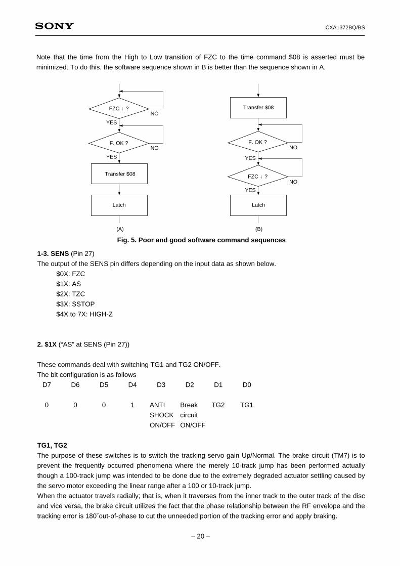
Note that the time from the High to Low transition of FZC to the time command $08 is asserted must be
minimized. To do this, the software sequence shown in B is better than the sequence shown in A.
FZC ↓ ?NO
YES
F. OK ?NO
Transfer $08
Latch
FZC ↓ ?NO
F. OK ?NO
Transfer $08
Latch
(A) (B)
YES YES
YES
Fig. 5. Poor and good software command sequences

– 21 –
CXA1372BQ/BS
EnvelopeDetection
[∗B]
[∗E]
RFI
(TZC)
Tracking error
(Latch)
QD
CK
(MIRR)[∗C]
[∗F]
[∗G]
BRK
D2
TM7Low: openHigh: make
[∗A]
[∗D]
WaveformShaping
WaveformShaping
Edge Detection
39
42 [∗H]
Fig. 6. TM7 operation (brake circuit)
From inner to outer track
0V
From outer to inner track
("MIRR")
("TZC")
Braking is applied from here.
[∗A]
[∗B]
[∗C]
[∗D]
[∗E]
[∗F]
[∗G]
[∗H]
Fig. 7. Internal waveform
3. $2X (“TZC” at SENS (Pin 27))
These commands deal with turning the tracking servo and sled servo ON/OFF, and creating the jump pulse
and fast forward pulse during access operations.
D7 D6 D5 D4 D3 D2 D1 D0
0 0 1 0 Tracking Sled
control control
00: OFF 00: OFF
01: Servo ON 01: Servo ON
10: F-JUMP 10: F-FAST FORWARD
11: R-JUMP 11: R-FAST FORWARD
↓ ↓TM1, TM3, TM4 TM2, TM5, TM6
– 22 –
CXA1372BQ/BS
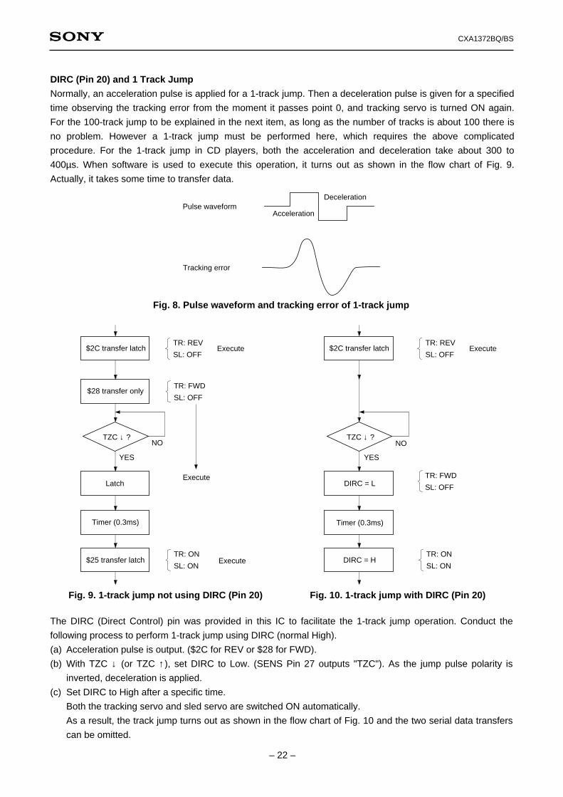
DIRC (Pin 20) and 1 Track Jump
Normally, an acceleration pulse is applied for a 1-track jump. Then a deceleration pulse is given for a specified
time observing the tracking error from the moment it passes point 0, and tracking servo is turned ON again.
For the 100-track jump to be explained in the next item, as long as the number of tracks is about 100 there is
no problem. However a 1-track jump must be performed here, which requires the above complicated
procedure. For the 1-track jump in CD players, both the acceleration and deceleration take about 300 to
400µs. When software is used to execute this operation, it turns out as shown in the flow chart of Fig. 9.
Actually, it takes some time to transfer data.
AccelerationPulse waveform
Tracking error
Deceleration
AAAAAA
$2C transfer latch
$28 transfer only
TZC ↓ ?NO
YES
Latch
Timer (0.3ms)
$25 transfer latch
TR: REV
SL: OFF
TR: FWD
SL: OFF
Execute
Execute
TR: ON
SL: ONExecute
AAAAAAAA
$2C transfer latch
TZC ↓ ?NO
YES
DIRC = L
Timer (0.3ms)
DIRC = H
TR: REV
SL: OFF
TR: FWD
SL: OFF
Execute
TR: ON
SL: ON
Fig. 9. 1-track jump not using DIRC (Pin 20) Fig. 10. 1-track jump with DIRC (Pin 20)
Fig. 8. Pulse waveform and tracking error of 1-track jump
The DIRC (Direct Control) pin was provided in this IC to facilitate the 1-track jump operation. Conduct the
following process to perform 1-track jump using DIRC (normal High).
(a) Acceleration pulse is output. ($2C for REV or $28 for FWD).
(b) With TZC ↓ (or TZC ↑ ), set DIRC to Low. (SENS Pin 27 outputs "TZC"). As the jump pulse polarity is
inverted, deceleration is applied.
(c) Set DIRC to High after a specific time.
Both the tracking servo and sled servo are switched ON automatically.
As a result, the track jump turns out as shown in the flow chart of Fig. 10 and the two serial data transfers
can be omitted.
– 23 –
CXA1372BQ/BS
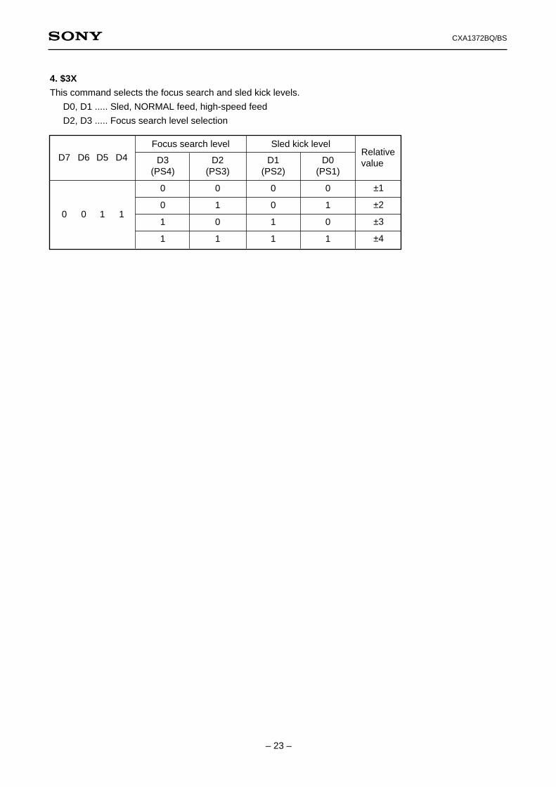
4. $3X
This command selects the focus search and sled kick levels.
D0, D1 ..... Sled, NORMAL feed, high-speed feed
D2, D3 ..... Focus search level selection
D7 D6 D5 D4
0 0 1 1
Focus search level Sled kick levelRelativevalueD3
(PS4)
0
0
1
1
D2(PS3)
0
1
0
1
D1(PS2)
0
0
1
1
D0(PS1)
0
1
0
1
±1
±2
±3
±4

– 24 –
CXA1372BQ/BS
Parallel Direct Interface
1. DIRC
$28 latch $2C latch
ON
OFF
ON
OFF
OFF
ON
ONOFF
XLT
DIRC
FWD JUMP
REV JUMP
TRACK SERVO
SLED SERVO
ONOFF
ONOFF
DOWNUP
LOCK
SLED SERVO
TG1, TG2
TRACKING GAIN
2. LOCK (Sled overrun prevention circuit)

– 25 –
CXA1372BQ/BS
CPU Serial Interface Timing Chart
tWCK
D0 D1 D2 D3 D4 D5 D6 D7
tWCK tSU
1/fck
th
tWL
tD
DATA
CLK
XLT
Item
Clock frequency
Clock pulse width
Setup time
Hold time
Delay time
Latch pulse width
Symbol
fck
fwck
tsu
th
tD
tWL
Min.
500
500
500
1000
1000
Typ. Max. Unit
MHz
ns
ns
ns
ns
ns
1
(DVCC – DGND = 4.5 to 5.5V)
System Control
Focus control
Tracking control
Tracking mode
Select
D7 D6 D5 D4
0 0 0 0
0 0 0 1
0 0 1 0
0 0 1 1
FS4FocusON
Anti-shock
PS4Focussearch + 2
PS3Focussearch + 1
PS2Sled kick + 2
PS1Sled kick + 1
FS3GainDown
BrakeON
FS2SearchON
TG2Gain set ∗ 1
FS1SearchUp
TG1
FZC
A. S
TZC
SSTOP
Tracking mode ∗ 2 Sled mode ∗ 3
Address
D3 D2 D1 D0
Data SENSoutput
∗ 2 Tracking mode
FWD JUMP
REV JUMP
D3
0
0
1
1
D2
0
1
0
1
OFF
ON
∗ 3 Sled mode
FWD MOVE
REV MOVE
D1
0
0
1
1
D0
0
1
0
1
OFF
ON
Item
∗ 1 Gain set
TG1 and TG2 can be set independently.
When the anti-shock is at 1 (00011xxx), both TG1 and TG2 are inverted when the internal anti-shock is at High.

– 26 –
CXA1372BQ/BS
Serial Data Truth Table
FOCUS CONTROL
TRACKING CONTROL
TRACKING MODEDIRC = 1 DIRC = 0 DIRC = 1
TM = 654321 654321 654321
AS = 0 AS = 1
TG = 2 1 TG = 2 1
Hex. Function
FS = 4 3 2 1
$00$01$02$03$04$05$06$07$08$09$0A$0B$0C$0D$0E$0F
$10$11$12$13$14$15$16$17$18$19$1A$1B$1C$1D$1E$1F
Serial data
0 0 0 0 0 0 0 00 0 0 0 0 0 0 10 0 0 0 0 0 1 00 0 0 0 0 0 1 10 0 0 0 0 1 0 00 0 0 0 0 1 0 10 0 0 0 0 1 1 00 0 0 0 0 1 1 10 0 0 0 1 0 0 00 0 0 0 1 0 0 10 0 0 0 1 0 1 00 0 0 0 1 0 1 10 0 0 0 1 1 0 00 0 0 0 1 1 0 10 0 0 0 1 1 1 00 0 0 0 1 1 1 1
0 0 0 1 0 0 0 00 0 0 1 0 0 0 10 0 0 1 0 0 1 00 0 0 1 0 0 1 10 0 0 1 0 1 0 00 0 0 1 0 1 0 10 0 0 1 0 1 1 00 0 0 1 0 1 1 10 0 0 1 1 0 0 00 0 0 1 1 0 0 10 0 0 1 1 0 1 00 0 0 1 1 0 1 10 0 0 1 1 1 0 00 0 0 1 1 1 0 10 0 0 1 1 1 1 00 0 0 1 1 1 1 1
0 0 0 00 0 0 10 0 1 00 0 1 10 1 0 00 1 0 10 1 1 00 1 1 11 0 0 01 0 0 11 0 1 01 0 1 11 1 0 01 1 0 11 1 1 01 1 1 1
0 0 0 00 1 0 11 0 1 01 1 1 10 0 0 00 1 0 11 0 1 01 1 1 10 0 1 10 1 1 01 0 0 11 1 0 00 0 1 10 1 1 01 0 0 01 1 0 1
000000 001000 000011000010 001010 000011010000 011000 100001100000 101000 100001000001 000100 000011000011 000110 000011010001 010100 100001100001 100100 100001000100 001000 000011000110 001010 000011010100 011000 100001100100 101000 100001001000 000100 000011001010 000110 000011011000 010100 100001101000 100100 100001
$20$21$22$23$24$25$26$27$28$29$2A$2B$2C$2D$2E$2F
0 0 1 0 0 0 0 00 0 1 0 0 0 0 10 0 1 0 0 0 1 00 0 1 0 0 0 1 10 0 1 0 0 1 0 00 0 1 0 0 1 0 10 0 1 0 0 1 1 00 0 1 0 0 1 1 10 0 1 0 1 0 0 00 0 1 0 1 0 0 10 0 1 0 1 0 1 00 0 1 0 1 0 1 10 0 1 0 1 1 0 00 0 1 0 1 1 0 10 0 1 0 1 1 1 00 0 1 0 1 1 1 1
– 27 –
CXA1372BQ/BS
GND
C26
GND
GN
D
WF
CK
XR
AO
F
GND
FO
K
FS
W
MO
N
MD
P
MD
S
LOC
K
NC
VC
OO
VC
OI
TE
ST
PD
O
VS
S
NC
NC
NC
VP
CO
VC
KI
FIL
O
FIL
I
PC
O
AV
SS
CLT
V
AV
DD
RF
2 5 6 7 8 9 10 11 12 13 14 15 16 18 19 20 21 22 231S
BS
O
SC
OR
WF
CK
EM
PH
DO
UT
MD
2
C16
M
C4M
FS
TT
XT
SL
XT
AO
XT
AI
VS
S
AP
TL
AP
TR
MN
T0
MN
T1
MN
T2
MN
T3
XR
AO
F
C2P
O
RF
CK
GF
S
XP
LCK
2526
2728
2930
4039
3837
3635
3431
3233
BIAS
ASYI
ASYO
ASYE
NC
PSSL
WDCK (48)
LRCK (48)
VDD
DATA (48)
BCLK (48)
DATA (64)
BCLK (64)
LRCK (64)
GTOP
XUGF
1314
1516
1718
1920
2123
SL+
SL0
SL–
FSET
ISET
SSTOP
AVEE
DIRC
LOCK
CLK
XLT
DATA
28293036 35 34 313233
DV
CC
CC
2
CC
1
FO
K
EF
M
AS
Y
DF
CT
MIR
R
DG
ND
SE
NS
C.O
UT
XR
ST
FDFCT
FE
FZC
ATSC
TDFCT
TE
TZC
DVEE
RFO
RFI
CP
CB
4039
3837
4142
4344
4546
4748
GND GND GND
GN
D
200p
1MA
VD
D
GND GND
VSS
GND
VCC
C2PO
MUTE
BCLK
DATA
WDCK
LRCK
DEMP
GN
D
MN
T0
MN
T1
MN
T2
MN
T3
GN
D
GT
OP
UG
FS
GF
S
RF
CK
XP
LCK
DO
UT
GN
D
GND
GND
VDD
MUTE
SCOR
SQCK
SUBQ
GFS
CLK
XLT
DATA
XRST
SENS
FOK
LDON
DF
CT
MIR
R
FE
TE
RF
LDON
VCC
VO
VCC
C17
GN
DG
ND
C15
C16
GN
D
C14
C13
C11
C12
GN
D
GN
DRV
2
RV
1
RF
TE
FE
GND C9
GND
C10
GND
C23
TR
AC
K-D
GN
D
FO
CU
S-D
GN
D
SLE
D-D
GN
D
SP
IND
-D
GN
D
SS
TO
P
GN
D
R1
GN
D
C28
GN
D
C27
R6
R7
GN
D
R3
R4
SPD
SLD
FD
TD
GN
D
GN
D
R10
GN
D
R12
CX
D25
00A
Q
VC
FG
D
FS
3
FLB
FE
O
FE
–
SR
CH
TG
U
TG
2
AV
CC
TA
0
TA
–
2 3 4 5 6 7 8 9 10 11 121
CX
A13
72B
Q
R1
R1
7069
6867
6566
7172
7374
7576
7778
7980
MIRR
CLKO
XLTO
DATO
CNIN
SEIN
CLOK
VDD
XLAT
DATA
XRST
SENS
MUTE
SQCK
SQSO
EXCK
2224
43 17
GND GND
414243444546474849505153545556575859606364 6162
27 2526
24
GN
D
R14
R13
GN
D
GND
52
PC
M
Ap
plic
atio
n C
ircu
it
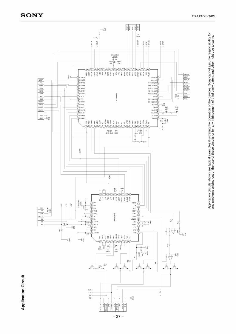
App
licat
ion
circ
uits
sho
wn
are
typi
cal e
xam
ples
illu
stra
ting
the
oper
atio
n of
the
devi
ces.
Son
y ca
nnot
ass
ume
resp
onsi
bilit
y fo
ran
y pr
oble
ms
aris
ing
out o
f the
use
of t
hese
circ
uits
or
for
any
infr
inge
men
t of t
hird
par
ty p
aten
t and
oth
er r
ight
due
to s
ame.
– 28 –
CXA1372BQ/BS
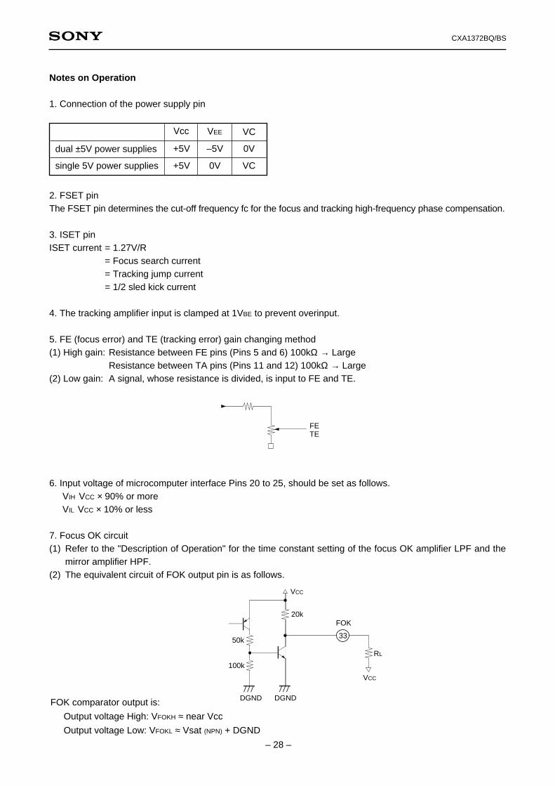
Notes on Operation
1. Connection of the power supply pin
2. FSET pinThe FSET pin determines the cut-off frequency fc for the focus and tracking high-frequency phase compensation.
3. ISET pinISET current = 1.27V/R
= Focus search current= Tracking jump current= 1/2 sled kick current
4. The tracking amplifier input is clamped at 1VBE to prevent overinput.
5. FE (focus error) and TE (tracking error) gain changing method(1) High gain: Resistance between FE pins (Pins 5 and 6) 100kΩ → Large
Resistance between TA pins (Pins 11 and 12) 100kΩ → Large(2) Low gain: A signal, whose resistance is divided, is input to FE and TE.
6. Input voltage of microcomputer interface Pins 20 to 25, should be set as follows.VIH VCC × 90% or moreVIL VCC × 10% or less
7. Focus OK circuit(1) Refer to the "Description of Operation" for the time constant setting of the focus OK amplifier LPF and the
mirror amplifier HPF.(2) The equivalent circuit of FOK output pin is as follows.
VCC
20k
50k
100k
DGND
RL
FOK
VCC
DGND
33
FOK comparator output is:
Output voltage High: VFOKH ≈ near Vcc
Output voltage Low: VFOKL ≈ Vsat (NPN) + DGND
dual ±5V power supplies
+5V 0V
VC
+5V –5V 0V
single 5V power supplies
Vcc VEE
VC
FETE

– 29 –
CXA1372BQ/BS
8. Mirror Circuit
(1) The equivalent circuit of MIRR output pin is as follows.
MIRR comparator output is:
Output voltage High: VMIRH ≈ VCC – Vsat (LPNP)
Output voltage Low: VMIRL ≈ near DGND
9. EFM Comparator
(1) Note that EFM duty varies when the CXA1372 Vcc differs from that of DSP IC (such as the CXD2500).
(2) The equivalent circuit of the EFM output pin is as follows.
∗ When the power supply current between Vcc and DGND is 5V.
EFM comparator output is:
Output voltage High: VEFMH ≈ VCC – VBE (NPN)
Output voltage Low: VEFML ≈ VCC – 4.8 (kΩ) × 700 (µA) – VBE (NPN)
700µA∗
4.8k 50
2mA∗
32
EFM
RL
DGND
Vcc
VEE DGND
20k
MIRR
RL
DGND
29

– 30 –
CXA1372BQ/BS
Sta
nd
ard
Cir
cuit
Des
ign
Dat
a fo
r F
ocu
s/T
rack
ing
Inte
rnal
Ph
ase
Co
mp
ensa
tio
n
S1
S2
S3
S4
S5
S6
S7
S8
S9
E1
E2
E3
E4
SD
Mea
sure
-m
ent
poin
t
Des
crip
tion
of o
utpu
tw
avef
orm
and
mea
sure
men
tm
etho
d
5 5 5 5 11 11 11 11
08 08 0C 0C 25 25 25 13 25 13
Uni
tM
ax.
Typ
.M
in.
Sym
bol
Bia
s co
nditi
onS
W c
ondi
tion
1.2k
Hz
gain
1.2k
Hz
phas
e
1.2k
Hz
gain
1.2k
Hz
phas
e
1.2k
Hz
gain
1.2k
Hz
phas
e
2.7k
Hz
gain
2.7k
Hz
phas
e
O O O O
21.5
63 16 63 13 –125
26.5
–130
dB deg
dB deg
dB deg
dB deg
Whe
n C
FLB
= 0
.1µF
TRACKINGFOCUSIte
mM
ode
O O O O

– 31 –
CXA1372BQ/BS
Example of Representative Characteristics
40
35
30
25
20
15
10
5
101 102 103 104 105–180
–135
–90
–45
0
45
90
135
180
f – Frequency [Hz]
G –
Gai
n [d
B]
φ –
Pha
se [d
egre
e]
FOCUS frequency characteristics
40
30
20
10
0
–10
–20101 102 103 104 105
f – Frequency [Hz]
G –
Gai
n [d
B]
φ –
Pha
se [d
egre
e]
Tracking frequency characteristics
φ
G
φ
G
0
180
120
60
0
–60
–120
–180
CTGU = 0.033µ
GAIN UPNORMAL
CFGD = 0.1µCFLB = 0.1µ
GAIN DOWNNORMAL

– 32 –
CXA1372BQ/BS
Package Outline Unit: mm
CXA1372BQ
CXA1372BS
SONY CODE
EIAJ CODE
JEDEC CODE
M
PACKAGE STRUCTURE
PACKAGE MATERIAL
LEAD TREATMENT
LEAD MATERIAL
PACKAGE WEIGHT
EPOXY RESIN
SOLDER / PALLADIUM PLATING
COPPER / 42 ALLOY
48PIN QFP (PLASTIC)
15.3 ± 0.4
12.0 – 0.1+ 0.4
0.8 0.3 – 0.1+ 0.15
± 0.12
13
24
2536
37
48
1 12
2.2 – 0.15+ 0.35
0.9
± 0.
2
0.1 – 0.1+ 0.2
13.5
0.15
0.15 – 0.05+ 0.1
QFP-48P-L04
∗QFP048-P-1212-B
0.7g
48PIN SDIP (PLASTIC) 600mil
13.0
+ 0
.3–
0.1
4.6
+ 0
.4–
0.1
0.25
+ 0
.1–
0.05
48 25
1 24
1.778
15.2
4 0° to 15°
0.5 ± 0.1
0.9 ± 0.15 3.0
MIN
0.5
MIN
SONY CODE
EIAJ CODE
JEDEC CODE
PACKAGE STRUCTURE
PACKAGE MATERIAL
LEAD TREATMENT
LEAD MATERIAL
PACKAGE WEIGHT
EPOXY RESIN
SOLDER PLATING
COPPER / 42 ALLOY
5.1g
SDIP-48P-02
SDIP048-P-0600-A
43.2+ 0.4– 0.1