customer specific device from on semiconductor
TRANSCRIPT

© Semiconductor Components Industries, LLC, 2009
July, 2009 − Rev. 01 Publication Order Number:
DDA002C/D
Customer Specific Device from ON Semiconductor
High PerformanceSwitch-Mode Power SupplyController for Backlight andLLC Converters
The DDA002C controller hosts a high performancecircuitry dedicated to driving half−bridge topologies, suchas lamp ballasts for backlighting applications or resonantconverters like the LLC circuit. The controller includeseverything needed to build a reliable and rugged converter,including a pre−heating period and various protections suchas an adjustable brown−out, for instance. Both, minimumand maximum switching frequencies, are adjustable bysingle pull down resistor, offering the ability to operatebetween 30 kHz and 500 kHz.
The controller includes a high−voltage driver thatsimplifies the design of the half−bridge configuration due todirect connection to the upper−side MOSFET. To avoidlarge shoot−through currents, the circuit includes a deadtimegenerator whose duration can be easily adjusted externally.Finally, two additional ground−referenced outputs allow theimplementation of full−bridge applications.Features• High−Frequency Operation from 30 kHz up to 500 kHz
• Selectable Minimum Switching Frequency
• Adjustable Deadtime from 100 ns to 2 �s
• 100 ms Delayed Startup for PFC Stage Stabilization
• Adjustable Preheating Timer via External Capacitor
• Startup Sequence via Adjustable Soft−Start
• 600 V High−Voltage Floating Drivers
• Synchronized Low−Current Outputs for Full BridgeApplications
• Adjustable Maximum On−Time Clamp forSynchronization Outputs
• Brown−Out Protection for Easier PFC Association
• Delayed Open−Loop Protection
• Latched Input for Severe Fault Conditions, e.g. OverCurrent
• Secondary Latched Input for Over Temperature Protection
• Auto−Recovery Enable Input
• VCC Operation up to 20 V
• Low Startup Current of 300 �A
• 0.5 A / 0.25 A Peak Current Sink / Source DriveCapability, Respectively
• Internal Temperature Shutdown
• SO19W package
• These Devices are Pb−Free, Halogen Free/BFR Freeand are RoHS Compliant
Typical Applications• Flat Panel Display Power Converters
• LLC Converters Control for LCD/Plasma TVs
• HCFL / CCFL Backlight Inverters
PIN CONNECTIONS
MARKING DIAGRAMS
DDA002C = Specific Device CodeA = Assembly LocationWL = Wafer LotYY = YearWW = Work WeekG = Pb−Free Package
SOIC−19, LESS PIN 17D SUFFIX
CASE 752AA
DDA002CAWLYYWWG
See detailed ordering and shipping information in the packagedimensions section on page 26 of this data sheet.
ORDERING INFORMATION
*For additional information on our Pb−Free strategyand soldering details, please download the ONSemiconductor Soldering and Mounting TechniquesReference Manual, SOLDERRM/D.
Boot
Hgd
HB
Vcc
Lgd
Gnd
Hgs
Lgs
EN2
BO
CIG
Dgs
SS
R_Fmin
R_Fmax
FB
OTP_latch
DT
EN1
DDA002C
DDA002C

DDA002C
http://onsemi.com2
19
181716
1514
111213
123456789
10
DDA002
SR drive
Figure 1. Typical Application Example
Rdt
RfmaxRfmin
Rfstart
Css
VCC VBULK
Vout

DDA002C
http://onsemi.com3
Pin Function Description
Pin No. Pin Name Function Pin Description
1 BO Brown−out Detects low input voltage conditions and stops the controller. An internalcurrent source sets the hysteresis.
2 CIG Warm−up time A capacitor connected to ground sets the pre−heat time for ballast applica-tions.
3 DGS Synchronous output clamp A resistor connected between this pin and ground adjusts the maximum on−time available on Lgs and Hgs pins.
4 SS Soft−start Monitors the soft−start capacitor voltage to recognize end of the soft−startperiod, discharges the soft−start capacitor during any IC restart.
5 R_Fmin Minimum frequency resistor Connecting a resistor between this pin and ground, sets the minimum oscil-lator frequency reached for VFB ≥ 5.1 V
6 R_Fmax Maximum frequencyresistor
A resistor connected between this pin and ground sets the maximum fre-quency excursion reached for VFB ≤ 1.2 V
7 FB Optocoupler connection An optocoupler connected (by collector) between this pin and ground (byemitter) changes the converter operating frequency. The switching frequencyincreases when optocoupler pulls the FB pin down to ground.
8 OTP_latch OTP latch input If the voltage on this pin decreases below 1.5 V, the circuit latches off. Thispin sources 170 �A current so an NTC resistor can be connected directly tothis pin.
9 DT Dead time A resistor connected between this pin and ground sets the deadtimebetween drivers.
10 EN1 Enable input 1 When the voltage level on this pin exceeds a reference level for more than50 �s, all pulses are stopped and the circuit permanently latches off.
11 EN2 Enable input 2 When the voltage level on this pin exceeds a reference voltage, the circuitstops pulsing. The IC auto−restarts via full startup sequence (PFC delay,pre−heat, soft−start) when EN2 is released.
12 Lgs Lower gate signal Duplicates the lower gate signal for synchronization purposes. On time islimited based on the Rdgs resistor value.
13 Hgs Upper gate signal Duplicates the upper gate signal for synchronization purposes. On time islimited based on the Rdgs resistor value.
14 GND Ground The controller ground
15 Lgd Low−side driver Drives the low−side half−bridge MOSFET
16 Vcc Controller Supply Energizing the controller. This pin accepts voltage up to 20 Vdc
17 HB Half−Bridge Connects to the half−bridge output
18 Hgd High−side driver Drives the high−side half−bridge MOSFET
19 Boot High side driver supply line This pin supplies the internal high−side driver

DDA002C
http://onsemi.com4
SW1
BOFilter
BO_ OK
TSD
PFC TIMER
Start
50 ms one shoot
100 msSR
UVDetect
Hgd
Boot
HB
Vcc
CIG_ESW2
CIG_ICIG
Dgs
SS_ESW3
SS SS_OK
R_Fmin
R_Fmax
Voltage controlledoscillator
I_Fmin
I_Fmax
I_Dgs
B
A
ON_TIMECLAMP
LgdDELAY
Vcc
Gnd
Hgs
Vcc
Lgs
Vcc
EN2SR
Q
FB FAULT TIMERStart
FAULT
50 ms
TMR _EN
FB
FB _Fault
FB Rfb
Vdd
OTPref_V
OTPref_I
OTP_latch
Vdd
NTC
DT
EN1
Figure 2. Internal Architecture
VCCon
Vref_Dgs
CIG_END
PFC_OK
VDD
VBULK
20 �s
VBO
IBOSwitch SW
open forVinBO > VBO
Vref_Fmin
Vref_Fmax
VEN1
Vref_DT
Q
50 �sNoiseFilter
VEN2
20 nsRC
Filter
I_DT
OSC_EN
CIG_END
PulseTrigger
LevelShifterPFC_OK

DDA002C
http://onsemi.com5
Maximum Ratings
Symbol Rating Value Unit
VHB Continuous voltage on the bridge pin, pin 17 −1 to 600 V
Qmax Maximum injected charge into the HB pin (Note 3) 11 nC
VBOOT−VHB Floating supply voltage, pin 17 and 19 −0.3 to 20 V
VHgd High side output voltage, pin 18 VHB−0.3 toVBOOT+0.3
V
VLgd Low side output voltage, pin 15 −0.3 to Vcc+0.3 V
dVHB/dt Maximum slew rate on the HB pin, pin 17 ±50 V/ns
Vcc Power Supply voltage, pin 16 −0.3 to 20 V
pin voltage, all pins (except pin 3, 6, 15, 16, 17, 18, and 19) −0.3 to 10 V
VDgs Synchronous clamp pin voltage, pin 3 −0.3 to 5 V
VR_Fmax Maximum frequency adjust pin voltage, pin 6 −0.3 to 5 V
R�J−A Thermal Resistance Junction−to−Ambient,(Soldered on traces with total area of 50 mm2, 1 oz copper)
Thermal Resistance Junction−to−Ambient,(Soldered on recommended layout, 1 oz copper)
137
117
°C/W
Storage Temperature Range −60 to +150 °C
TJmax Maximum Junction Temperature +150 °C
ESD Capability, HBM model (Except all HV pins i.e., HB, Hgd and Boot) (Note 1) 2 kV
ESD Capability, Machine Model 200 V
Stresses exceeding Maximum Ratings may damage the device. Maximum Ratings are stress ratings only. Functional operation above theRecommended Operating Conditions is not implied. Extended exposure to stresses above the Recommended Operating Conditions may affectdevice reliability.1. This device series contains ESD protection and exceeds the following tests: Human Body Model 2000 V per JEDEC (22A114C − Human
Body Model and 22A115A Machine Model)2. This device contains latch−up protection and exceeds 100 mA per JEDEC Standard JESD78.3. The maximum injected charge corresponds to the injected current integrated over time into the half−bridge pin. Please refer to Figure 60
and related notes.

DDA002C
http://onsemi.com6
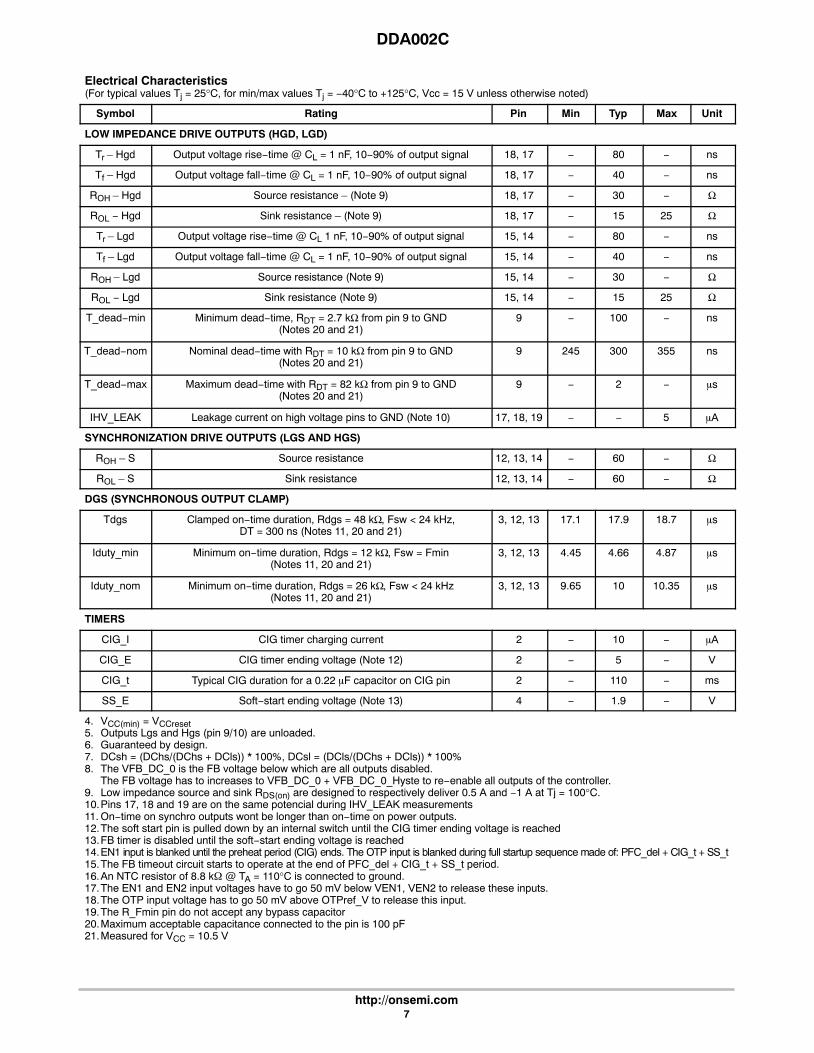
Electrical Characteristics(For typical values Tj = 25°C, for min/max values Tj = −40°C to +125°C, Vcc = 15 V unless otherwise noted)
Symbol Rating Pin Min Typ Max Unit
SUPPLY SECTION
VCCON Turn−on threshold level, Vcc going up 16 11 12 13 V
VCC(min) Minimum operating voltage after turn−on (Note 4) 16 8.5 9.5 10.5 V
VbootON Startup voltage on the floating section 19,17 8 9 10 V
Vboot(min) Cutoff voltage on the floating section 19,17 7.4 8.4 9.4 V
Istartup Startup current, Vcc < VCCON 16 − − 300 �A
ICC1 Internal IC consumption, no output load on pin 18/17 – 15/14,Fsw = 300 kHz (Note 5)
16 − 5 − mA
ICC2 Internal IC consumption, 1 nF output load on pin 18/17 – 15/14,Fsw = 300 kHz (Note 5)
16 − 14 − mA
ICC3 Internal IC consumption in fault mode(All drivers disabled, VCC > VCC(min))
16 − 2.5 − mA
VOLTAGE CONTROL OSCILLATOR (VCO)
Fsw min Minimum switching frequency, R_Fmin = 41 kΩ on pin 5,Vpin 7 > 5.5 V, DT = 300 ns (Notes 19 and 21)
5 58 60 62 kHz
Fsw max Maximum switching frequency, R_Fmax = 2.5 kΩ on pin 6,Vpin 7 < 1.2 V, DT = 100 ns, Rt = 41 kΩ (Notes 20 and 21)
6 450 500 550 kHz
SVCO Maximum VCO conversion slope, �f / ΔVfb (Note 6) − − 120 − kHz / V
FBSW min Feedback pin swing above which �f = 0, Fsw = Fmin, DC = 50% 7 − 5.1 − V
FBSW max Feedback pin swing below which �f = 0, Fsw = Fmax, DC = 50%(Note 6)
7 − 1.2 − V
DCsl, DCsh Operating duty−cycle symetry, 5.5 V> Vpin 7 > 0.5 V (Note 7) 18,17;15,14
48 50 52 %
Min Ton Minimum On time 18,17;15,14
− 880 − ns
VFB_DC_0 Skip comparator threshold on the feedback pin (Note 8) 7 − 1.2 − V
VFB_DC_0_Hyste
Hysteresis on the skip comparator 7 − 50 − mV
VREF Reference voltage for Fmin current generation 5 − 2 − V
FEEDBACK SECTION
Rfb Internal pull−up resistor 7 − 10 − kΩ
Vfb_O Open−loop voltage on the feedback pin, no optocoupler connection 7 − 7.3 − V
4. VCC(min) = VCCreset5. Outputs Lgs and Hgs (pin 9/10) are unloaded.6. Guaranteed by design.7. DCsh = (DChs/(DChs + DCls)) * 100%, DCsl = (DCls/(DChs + DCls)) * 100%8. The VFB_DC_0 is the FB voltage below which are all outputs disabled.
The FB voltage has to increases to VFB_DC_0 + VFB_DC_0_Hyste to re−enable all outputs of the controller.9. Low impedance source and sink RDS(on) are designed to respectively deliver 0.5 A and −1 A at Tj = 100°C.10.Pins 17, 18 and 19 are on the same potencial during IHV_LEAK measurements11. On−time on synchro outputs wont be longer than on−time on power outputs.12.The soft start pin is pulled down by an internal switch until the CIG timer ending voltage is reached13.FB timer is disabled until the soft−start ending voltage is reached14.EN1 input is blanked until the preheat period (CIG) ends. The OTP input is blanked during full startup sequence made of: PFC_del + CIG_t + SS_t15.The FB timeout circuit starts to operate at the end of PFC_del + CIG_t + SS_t period.16.An NTC resistor of 8.8 k� @ TA = 110°C is connected to ground.17.The EN1 and EN2 input voltages have to go 50 mV below VEN1, VEN2 to release these inputs.18.The OTP input voltage has to go 50 mV above OTPref_V to release this input.19.The R_Fmin pin do not accept any bypass capacitor20.Maximum acceptable capacitance connected to the pin is 100 pF21.Measured for VCC = 10.5 V
DDA002C
http://onsemi.com7
Electrical Characteristics(For typical values Tj = 25°C, for min/max values Tj = −40°C to +125°C, Vcc = 15 V unless otherwise noted)
Symbol UnitMaxTypMinPinRating
LOW IMPEDANCE DRIVE OUTPUTS (HGD, LGD)
Tr – Hgd Output voltage rise−time @ CL = 1 nF, 10−90% of output signal 18, 17 − 80 − ns
Tf – Hgd Output voltage fall−time @ CL = 1 nF, 10−90% of output signal 18, 17 − 40 − ns
ROH – Hgd Source resistance – (Note 9) 18, 17 − 30 − Ω
ROL − Hgd Sink resistance – (Note 9) 18, 17 − 15 25 Ω
Tr – Lgd Output voltage rise−time @ CL 1 nF, 10−90% of output signal 15, 14 − 80 − ns
Tf – Lgd Output voltage fall−time @ CL = 1 nF, 10−90% of output signal 15, 14 − 40 − ns
ROH – Lgd Source resistance (Note 9) 15, 14 − 30 − Ω
ROL − Lgd Sink resistance (Note 9) 15, 14 − 15 25 Ω
T_dead−min Minimum dead−time, RDT = 2.7 kΩ from pin 9 to GND(Notes 20 and 21)
9 − 100 − ns
T_dead−nom Nominal dead−time with RDT = 10 kΩ from pin 9 to GND(Notes 20 and 21)
9 245 300 355 ns
T_dead−max Maximum dead−time with RDT = 82 kΩ from pin 9 to GND(Notes 20 and 21)
9 − 2 − �s
IHV_LEAK Leakage current on high voltage pins to GND (Note 10) 17, 18, 19 − − 5 �A
SYNCHRONIZATION DRIVE OUTPUTS (LGS AND HGS)
ROH – S Source resistance 12, 13, 14 − 60 − Ω
ROL – S Sink resistance 12, 13, 14 − 60 − Ω
DGS (SYNCHRONOUS OUTPUT CLAMP)
Tdgs Clamped on−time duration, Rdgs = 48 kΩ, Fsw < 24 kHz,DT = 300 ns (Notes 11, 20 and 21)
3, 12, 13 17.1 17.9 18.7 �s
Iduty_min Minimum on−time duration, Rdgs = 12 kΩ, Fsw = Fmin(Notes 11, 20 and 21)
3, 12, 13 4.45 4.66 4.87 �s
Iduty_nom Minimum on−time duration, Rdgs = 26 kΩ, Fsw < 24 kHz(Notes 11, 20 and 21)
3, 12, 13 9.65 10 10.35 �s
TIMERS
CIG_I CIG timer charging current 2 − 10 − �A
CIG_E CIG timer ending voltage (Note 12) 2 − 5 − V
CIG_t Typical CIG duration for a 0.22 �F capacitor on CIG pin 2 − 110 − ms
SS_E Soft−start ending voltage (Note 13) 4 − 1.9 − V
4. VCC(min) = VCCreset5. Outputs Lgs and Hgs (pin 9/10) are unloaded.6. Guaranteed by design.7. DCsh = (DChs/(DChs + DCls)) * 100%, DCsl = (DCls/(DChs + DCls)) * 100%8. The VFB_DC_0 is the FB voltage below which are all outputs disabled.
The FB voltage has to increases to VFB_DC_0 + VFB_DC_0_Hyste to re−enable all outputs of the controller.9. Low impedance source and sink RDS(on) are designed to respectively deliver 0.5 A and −1 A at Tj = 100°C.10.Pins 17, 18 and 19 are on the same potencial during IHV_LEAK measurements11. On−time on synchro outputs wont be longer than on−time on power outputs.12.The soft start pin is pulled down by an internal switch until the CIG timer ending voltage is reached13.FB timer is disabled until the soft−start ending voltage is reached14.EN1 input is blanked until the preheat period (CIG) ends. The OTP input is blanked during full startup sequence made of: PFC_del + CIG_t + SS_t15.The FB timeout circuit starts to operate at the end of PFC_del + CIG_t + SS_t period.16.An NTC resistor of 8.8 k� @ TA = 110°C is connected to ground.17.The EN1 and EN2 input voltages have to go 50 mV below VEN1, VEN2 to release these inputs.18.The OTP input voltage has to go 50 mV above OTPref_V to release this input.19.The R_Fmin pin do not accept any bypass capacitor20.Maximum acceptable capacitance connected to the pin is 100 pF21.Measured for VCC = 10.5 V

DDA002C
http://onsemi.com8
Electrical Characteristics(For typical values Tj = 25°C, for min/max values Tj = −40°C to +125°C, Vcc = 15 V unless otherwise noted)
Symbol UnitMaxTypMinPinRating
TIMERS
PFC_del Internal delay timer after brown−out confirmation,EN2 released or Vcc restart
− − 100 − ms
PROTECTIONS
VEN1 Reference voltage for the enable 1 input (latch), (Note 14), (Note 17) 10 0.95 1 1.05 V
VEN2 Reference voltage for the enable 2 input (Note 17) 11 0.95 1 1.05 V
HysteENX Hysteresis for EN1, EN2 inputs 10, 11 − 50 − mV
VdelEN1 Delay before latch confirmation on EN1 input (Note 14) 10 − 50 − �s
VdelEN2 Delay between the EN2 activation and driver disable 11 − 80 120 ns
VBO Brown−Out level 1 0.95 1 1.05 V
IBO Hysteresis current, Vpin 1 = 0.9 V, 0°C < TJ < 125°CHysteresis current, Vpin 1 = 0.9 V, −40°C < TJ < 125°C
1 17.8516.31
2121
24.1524.15
�A
IBObias Brown−Out input bias current 1 − 0.02 − �A
OTPref_I OTP Reference current (Note 16), 0°C < TJ < 125°COTP Reference current (Note 16), −40°C < TJ < 125°C
8 155.7143.7
173173
190.3190.3
�A
OTPref_V OTP reference voltage (Note 14), (Note 18) 8 1.425 1.5 1.575 V
OTP_hyste OTP comparator hysteresis 8 − 50 − mV
OTPnoise Noise filter on the OTP output (Note 14) 8 − 50 − �s
FB_Fault Above this level, the FB fault timer is activated (Note 15) 7 − 6 − V
FB_timer FB timeout duration (Note 15) 7 − 50 − ms
TSD Temperature shutdown threshold − 140 − − °C
TSDhyste Temperature shutdown hysteresis − − 30 − °C
4. VCC(min) = VCCreset5. Outputs Lgs and Hgs (pin 9/10) are unloaded.6. Guaranteed by design.7. DCsh = (DChs/(DChs + DCls)) * 100%, DCsl = (DCls/(DChs + DCls)) * 100%8. The VFB_DC_0 is the FB voltage below which are all outputs disabled.
The FB voltage has to increases to VFB_DC_0 + VFB_DC_0_Hyste to re−enable all outputs of the controller.9. Low impedance source and sink RDS(on) are designed to respectively deliver 0.5 A and −1 A at Tj = 100°C.10.Pins 17, 18 and 19 are on the same potencial during IHV_LEAK measurements11. On−time on synchro outputs wont be longer than on−time on power outputs.12.The soft start pin is pulled down by an internal switch until the CIG timer ending voltage is reached13.FB timer is disabled until the soft−start ending voltage is reached14.EN1 input is blanked until the preheat period (CIG) ends. The OTP input is blanked during full startup sequence made of: PFC_del + CIG_t + SS_t15.The FB timeout circuit starts to operate at the end of PFC_del + CIG_t + SS_t period.16.An NTC resistor of 8.8 k� @ TA = 110°C is connected to ground.17.The EN1 and EN2 input voltages have to go 50 mV below VEN1, VEN2 to release these inputs.18.The OTP input voltage has to go 50 mV above OTPref_V to release this input.19.The R_Fmin pin do not accept any bypass capacitor20.Maximum acceptable capacitance connected to the pin is 100 pF21.Measured for VCC = 10.5 V

DDA002C
http://onsemi.com9
TYPICAL CHARACTERISTICS
Figure 3. Fswmin vs. Temperature Figure 4. Vbooton vs. Temperature
TEMPERATURE (°C) TEMPERATURE (°C)
958065205−10−25−4060.0
60.1
60.2
60.3
60.4
60.5
60.6
60.7
8.65
8.70
8.75
8.80
8.90
8.95
9.05
9.10
Figure 5. VCC(min) vs. Temperature Figure 6. VCCON vs. Temperature
TEMPERATURE (°C) TEMPERATURE (°C)
9.34
9.35
9.36
9.37
9.38
9.41
9.42
9.43
11.65
11.70
11.75
11.80
11.85
11.90
Figure 7. OTPref_I vs. Temperature Figure 8. Iduty min vs. Temperature
TEMPERATURE (°C) TEMPERATURE (°C)
150
155
160
165
170
175
180
4.604.61
4.63
4.64
4.66
4.68
4.69
4.71
Fsw
min
(kH
z)
Vbo
oton
(V
)
VC
C(m
in) (
V)
VC
CO
N (
V)
OT
Pre
f_I (�A
)
Idut
y m
in (�s)
35 50 110 125 958065205−10−25−40 35 50 110 125
8.85
9.00
958065205−10−25−40 35 50 110 125
9.39
9.40
958065205−10−25−40 35 50 110 125
958065205−10−25−40 35 50 110 125 958065205−10−25−40 35 50 110 125
4.62
4.65
4.67
4.70

DDA002C
http://onsemi.com10
TYPICAL CHARACTERISTICS
Figure 9. Tdgs vs. Temperature Figure 10. Iduty nom vs. Temperature
TEMPERATURE (°C) TEMPERATURE (°C)
1108035205−10−25−4017.8717.88
17.90
17.95
17.93
17.94
17.96
17.97
9.88
9.89
9.90
9.92
9.93
9.95
9.96
9.97
Figure 11. VFB_DC_0 vs. Temperature Figure 12. FBSW max vs. Temperature
TEMPERATURE (°C) TEMPERATURE (°C)
1.075
1.080
1.085
1.090
1.095
1.100
1.097
1.099
1.100
1.101
1.102
1.103
1.104
Figure 13. FBSW min vs. Temperature Figure 14. Fsw max vs. Temperature
TEMPERATURE (°C) TEMPERATURE (°C)
4.94
4.96
4.98
5.00
5.02
5.04
5.06
494
496
498
500
502
504
508
510
Tdg
s (�
s)
Idut
y no
m (�s)
VF
B_D
C_0
(V
)
FB
SW
max
(V
)
FB
SW
min
(V
)
Fsw
max
(kH
z)
6550 95 125
17.89
17.92
17.91
1108035205−10−25−40 6550 95 125
9.91
9.94
1108035205−10−25−40 6550 95 125 1108035205−10−25−40 6550 95 125
1108035205−10−25−40 6550 95 125 1108035205−10−25−40 6550 95 125
506
1.098

DDA002C
http://onsemi.com11
TYPICAL CHARACTERISTICS
Figure 15. Istartup vs. Temperature Figure 16. Vboot(min) vs. Temperature
TEMPERATURE (°C) TEMPERATURE (°C)
1109535205−10−25−400
50
100
150
200
250
300
8.15
8.20
8.25
8.35
8.40
8.45
8.55
8.60
Figure 17. IBO vs. Temperature Figure 18. Rfb vs. Temperature
TEMPERATURE (°C) TEMPERATURE (°C)
18.0
18.5
19.0
19.5
20.0
20.5
21.0
21.5
0
2
4
6
8
12
14
16
Figure 19. VFB_DC_0_Hyste vs. Temperature Figure 20. VdelEN1 vs. Temperature
TEMPERATURE (°C) TEMPERATURE (°C)
0
10
20
30
40
50
70
80
0
10
20
30
40
50
60
70
Ista
rtup
(�A
)
Vbo
ot(m
in) (
V)
IBO
(�A
)
Rfb
(k�
)
VF
B_D
C_0
_Hys
te (
mV
)
Vde
lEN
1 (�
s)
806550 125 1109535205−10−25−40 806550 125
8.30
8.50
1109535205−10−25−40 806550 125 1109535205−10−25−40 806550 125
10
1109535205−10−25−40 806550 125
60
1109535205−10−25−40 806550 125

DDA002C
http://onsemi.com12
TYPICAL CHARACTERISTICS
Figure 21. HysteENX vs. Temperature Figure 22. VEN2 vs. Temperature
TEMPERATURE (°C) TEMPERATURE (°C)
1108065205−10−25−400
10
20
30
40
50
60
0.99300.9935
0.9940
Figure 23. VEN1 vs. Temperature Figure 24. PFC_del vs. Temperature
TEMPERATURE (°C) TEMPERATURE (°C)
0.989
0.990
0.991
0.992
0.993
0.994
0.996
0.997
92
94
96
98
100
102
106
108
Figure 25. SS_E vs. Temperature Figure 26. CIG_E vs. Temperature
TEMPERATURE (°C) TEMPERATURE (°C)
1.835
1.840
1.845
1.850
1.855
1.860
5.065
5.070
5.075
5.080
5.085
5.090
Hys
teE
NX
(m
V)
VE
N2
(V)
VE
N1
(V)
PF
C_d
el (
ms)
SS
_E (
V)
CIG
_E (
V)
35 50 95 125 1108065205−10−25−40 35 50 95 125
0.9945
0.9950
0.9955
0.9960
0.9965
0.9970
0.9975
0.9980
0.9985
1108065205−10−25−40 35 50 95 125
0.995
1108065205−10−25−40 35 50 95 125
104
1108065205−10−25−40 35 50 95 125 1108065205−10−25−40 35 50 95 125

DDA002C
http://onsemi.com13
TYPICAL CHARACTERISTICS
Figure 27. CIG_I vs. Temperature Figure 28. IHV_LEAK vs. Temperature
TEMPERATURE (°C) TEMPERATURE (°C)
1105035205−10−25−409.2
9.4
9.6
9.8
10.0
10.4
10.6
10.8
0
0.5
1.0
1.5
2.0
2.5
3.0
Figure 29. FB_timer vs. Temperature Figure 30. FB_Fault vs. Temperature
TEMPERATURE (°C) TEMPERATURE (°C)
46.0
47.0
47.5
48.5
49.0
50.0
51.0
6.045
6.050
6.055
6.060
6.065
6.070
6.075
6.080
Figure 31. OTPref_V vs. Temperature Figure 32. VBO vs. Temperature
TEMPERATURE (°C) TEMPERATURE (°C)
1.484
1.486
1.488
1.490
1.492
1.494
1.496
0.990
0.991
0.992
0.993
0.994
0.996
0.997
0.998
CIG
_I (�A
)
IHV
_LE
AK
(�A
)
FB
_tim
er (
ms)
FB
_Fau
lt (V
)
OT
Pre
f_V
(V
)
VB
O (
V)
10.2
958065 125 1105035205−10−25−40 958065 125
1105035205−10−25−40 958065 125 1105035205−10−25−40 958065 125
1105035205−10−25−40 958065 125 1105035205−10−25−40 958065 125
0.995
46.5
48.0
49.5
50.5

DDA002C
http://onsemi.com14
TYPICAL CHARACTERISTICS
Figure 33. VdelEN2 vs. Temperature Figure 34. T_dead−nom vs. Temperature
TEMPERATURE (°C) TEMPERATURE (°C)
0
10
30
40
50
70
80
100
302
304
306
308
310
312
314
Vde
lEN
2 (n
s)
T_d
ead−
nom
(ns
)
1105035205−10−25−40 958065 125
20
60
90
1105035205−10−25−40 958065 125

DDA002C
http://onsemi.com15
Application Information
The DDA002C includes all necessary features that helpbuilding a rugged and safe switch−mode power converterfor an LCD TV backlighting or LLC resonant SMPSapplications. The bullets below detail the benefits broughtby implementing the DDA002C controller:• High−voltage drivers: thanks to the ON Semiconductor
proprietary technology, the DDA002C controller candirectly drive the upper−side transistor of a half−bridgeconfiguration biased up to 600 V.
• Wide frequency range: a high−speed Voltage ControlOscillator allows operating frequency excursion from30 kHz up to 500 kHz on the Lgd and Hgd outputs,with a 50% duty−cycle. These two outputs are availableas synchronization signals via two ground−referencedlow−current outputs (Lgs and Hgs).
• Internal skip comparator: all drivers are disabledwhen feedback voltage goes below 1.2 V level. Theskip comparator includes 50 mV hysteresis.
• PFC−delay: the controller includes a fixed 100 msdelay to allow bulk voltage stabilization after the PFCstage has been started. The PFC timer is reset atpower−on, when a brown−out condition occurs andwhen the EN2 input is released. The controller is ready(VREF is OK) but no pulses are delivered by theoutputs during this delay period.
• Pre−heat period: once the PFC delay has elapsed, thecircuit starts to pulse with start up frequency topre−heat the lamps (in HCFL ballast applications). Thisperiod is also called CIG period.
• Adjustable soft−start: at the end of the pre−heatperiod, the soft−start sequence takes place. Thecontroller starts pulsing with Fstart and reduces itsfrequency down to Fmin. The feedback loop is supposedto take over during this period. The Fstart frequency isdictated by the parallel combination of Rfstart and Rfminresistors, the soft−start length is given by a capacitorconnected to the ground. The soft−start sequence isactivated after every controller restart.
• Open−Loop detection: the controller starts to monitorthe feedback voltage at the end of the soft−start period.If it remains stuck above 6 V (it means the feedbackloop is not closed) the internal timer starts thecountdown. The controller latches off if this situationlasts longer than 50 ms.
• Adjustable dead−time: using a single resistor wired tothe ground, the user has ability to include neededdead−time that helps to fight cross−conduction betweenthe upper and lower bridge transistors.
• Adjustable minimum and maximum frequencyexcursion: in resonant applications, it is important tostay away from the resonating peak to keep theconverter operating in the right region (ZVS). It is alsoneeded, for ballast applications, to keep the Fminaccuracy high since it dictates maximum lamp power.Thanks to a single external resistor, the designer canprogram its lowest frequency point, obtained due to alack of feedback voltage (during the startup sequence orin short−circuit conditions). Internally trimmedcapacitor offers a ±3.3 % precision on the selection ofthe minimum switching frequency. The adjustableupper frequency limit is less precise (±10%).
• Low startup current: the device requires only 300 �Astart−up current. This feature decreases the powerdissipation and/or shortening of the start−up time whenthe controller is powered from an auxiliary winding andstarts using a startup resistor connected directly to thebulk voltage.
• Brown−Out detection: the IC incorporates a brown outcomparator, which prevents the outputs from switchingin case the high−voltage rail is not within the rightboundaries. The turn on and off levels of the bulkvoltage can be adjusted independently thanks to theinternal current sink IBO.
• Enable1 input: when a voltage above 1 V is applied tothis pin, for a time longer than 50 �s, the controllerpermanently latches−off. The latch resets when Vcc iscycled below Vcc(min) or when there is a brown−outevent detected. The EN1 input is blanked during thePFC delay and preheat periods.
• Enable2 input: when a voltage higher than 1 V isapplied to this pin, the controller immediately stops allpulses. The controller restores operation (includingPFC delay, preheat and soft−start) when enable 2 inputvoltage decreases down again.
• OTP latch input: by connecting an NTC resistorbetween ground and the OTP_latch input, the designerhas ability to latch−off the controller in anover−temperature condition. The OTP input is blankedduring the PFC delay, preheat and soft−start periods.
• Synchronization outputs: two low−current groundreferenced outputs (Lgs and Hgs) are available toimplement a full−bridge converter in higher powerconfigurations. A resistor connected to the Dgs pin setsthe maximum allowable on−time that is delivered bythese two outputs when used for synchronizationpurpose.

DDA002C
http://onsemi.com16
Voltage−Controlled OscillatorThe VCO section features a high−speed circuitry allowing
operation from 60 kHz up to 1 MHz. However, as there is aninternal division by two, it creates Q and Q outputs. The finaleffective signal on the outputs Lgd, Hgd, Lgs and Hgs
therefore switches between 30 kHz and 500 kHz. The VCOis configured in such a way that if the feedback pin voltagegoes down, the switching frequency goes up. Figure 35shows simplified architecture of the VCO.
DT
Vdd
Vref
Ct_DT
S
R
Q
Rfmin
Vdd
Vref
Ct_ T_On
Vdd
10 k
Vdd
FB
R_Fmax
FB_Fault To_FB_Fault_Timer
Skip
Dgs Vref
Ct_Dgs
Vdd
On_time_clamp
S
R
QDCLK
frominternal logic
DT
A
BTo drivers
SR_A
SR_BTo SR drivers
Figure 35. Simplified VCO Architecture
Vref = 2.5 V
Vref_FB_Fault = 6 V
Vref_DC_0 = 1.2 V
Vref = 1.2 V
Vref = 1.2 V
Vref = 2.5 V
Q
QVref = 2.5 V
The VCO conversion characteristic is shown in Figure 36.The FB fault is detected in case the feedback voltage ishigher than 6 V. This will happen if the converter isoverloaded or the feedback path is not closed i.e. a brokenoptocoupler. The internal fault timer starts to count once the
FB fault is detected and it latches off the controller if the faultlasts more than 50 ms. To overcome triggering of the FBfault protection during the application start, the FB timer isdisabled until the soft−start period ends (VSS > 1.9 V).

DDA002C
http://onsemi.com17
Fmin
Fmax
5.1 6
Frequencydecreases
Novariations
FB faultdetection
Outputsdisabled
1.2
Figure 36. VCO Transfer Characteristic
VFB (V)
OperatingFrequency
The output frequency remains at Fmin and the duty cycleis at its maximum value (50% − deadtime) when the FB pinvoltage ranges between 5.1 and 6 V. The frequency of theconverter varies between Fmin and Fmax values if thefeedback voltage changes from 5.1 to 1.2 V. If the feedback
voltage further decreases, the operating frequency staysconstant and is given by the R_fmax resistor value. The ICdisables all drivers once the feedback voltage goes below1.2 V threshold − skip mode. Please refer also to typicalVCO operating waveforms in Figure 37.
V_FB
6V 5.1V
1.2V
C_DT
DT
A
B
C_Dgs
SR_A
SR_B
Variable FopDT=50%
FixedFop=FminDT=50% Fop = Fmax
Ct_T_On
FB_Fault
Figure 37. VCO Operating WaveformsFB_Faultdetected
OperationMode

DDA002C
http://onsemi.com18
The selection of the three setting resistors (Fmax, Fmin anddeadtime) require the usage of the selection charts displayedbelow:
50
100
150
200
300
350
400
2 4 6 8 10 12 16 18 20
Fm
ax (
kHz)
Figure 38. Maximum Switching FrequencyResistor Selection Depending on the Adopted
Minimum Switching Frequency
RFmax (k�)14 22
250
450
500
Fmin = 200 kHz
Fmin = 30 kHz
Figure 39. Minimum Switching Frequency ResistorSelection (Fmin = 20 kHz to 100 kHz)
20
30
40
50
60
70
80
20 40 60 80 100 120
Fm
in (
kHz)
RFmin (k�)140
90
100
Figure 40. Minimum Switching Frequency ResistorSelection (Fmin = 100 kHz to 500 kHz)
100
150
200
250
300
350
400
2 7 12 17 22
Fm
in (
kHz)
RFmin (k�)
450
500
0
200
400
600
800
1000
1200
1400
1600
1800
2000
1 11 21 31 41 51 61 71 81
DT
(ns
)
Figure 41. Deadtime Resistor SelectionRdt (k�)
Deadtime ControlDeadtime control is an absolute necessity when the
half−bridge configuration comes into play. The deadtimetechnique consists of including a time period during whichboth high and low side switches are off. Of course, thedeadtime amount should be different depending on theswitching frequency, hence the ability to adjust it on thiscontroller. The option ranges between 100 ns and 2 �s. Thedeadtime is actually made by the internal timer which is apart of the VCO. Please refer to Figures 35 and 37 for moredetails. During the Ct_DT capacitor charge time, the internallatch is set and invalidates the AND gates: all outputs arelow. When the comparator goes back to the low level, A andB outputs are validated, while the timing capacitor Ct_T_Onrecharges. By connecting a resistor RDT to the ground, itcreates a current whose image serves to charge the Ct_DTcapacitor − we control the deadtime. It typically rangesbetween 100 ns (RDT = 2.7 k�) and 2 �s (RDT = 70 k�).
100 ms PFC TimerThe DDA002C device features an internal digital timer
that prolongs the device start by 100 ms after the controlleris enabled by Vccon and/or a BO event. This fixed delayallows the PFC stage to fully stabilize the bulk voltagebefore the resonant power stage is activated. The PFC delayalso occurs when the EN2 input is released.
Adjustable Preheat Period − CIG TimerAs this IC is tailored not only for the resonant SMPS
applications but also to drive HCFL lamp ballasts, itincludes an adjustable preheat timer that allows the designerto accurately setup needed filament preheat time. The timeruses an external capacitor (Cpreheat) that is charged from aninternal current source (CIG_I). The IC outputs are forced(via VCO) to operate at the frequency that is given by theparallel combination of resistors Rfmin and Rfstart until theCpreheat capacitor voltage reaches 5 V. Figure 42 shows theinternal arrangement of the GIC timer.

DDA002C
http://onsemi.com19
CIG_ E = 5 V
CIG _I = 10 uA
CIGto VCO
100ms PFC timer
to Soft −Startdischarge
BO OK
Vcc Reset
Figure 42. CIG Timer Internal Connection
CPREHEAT
VDD
PFC_OK
The preheat time can be easily calculated using Equation 1:
TCIG � CPreheat � 0.5 (eq. 1)
Where:
TCIG is the preheat period time in seconds
CPreheat is the preheat capacitor value in �F
Note that the PFC delay period takes place prior to preheatperiod. Soft−start period starts immediately after the preheatcapacitor voltage is higher than 5 V. If using this IC to drive
a resonant SMPS or another application that does not requirepreheating, use 100 nF capacitor on the CIG pin to overcomefalse triggering by external noise.
Soft−start SequenceIn resonant converters, a soft−start is needed to avoid
suddenly applying the full current into the resonant tank.The soft−start is fully controlled by the external componentvalues when using DDA002C controller − refer toFigure 43.
R_Fmin
SS
Rfstart
FB timerenable
from CIGblock
Rfmin
Figure 43. Soft−start Block Internal Connection
CSSSS_E = 1.9 V
CIG_END
The soft−start capacitor is discharged by an internalswitch before the soft−start period begins. The dischargingpath is released at the end of the CIG period. The switchingfrequency is then given by the parallel combination ofresistors Rfmin and Rfstart. Since the soft−start capacitorcharges from the R_Fmin reference voltage, via the Rfstartresistor, the current driven from the R_Fmin pinexponentially decreases, as does the switching frequency. Incase the feedback path does not take control, the switchingfrequency will reach a value that is given by the Rfmin
resistor. The feedback fault timer is disabled during the PFCdelay, preheat, and soft−start periods in order to overcomeunwanted controller operation interruption. This isaccomplished by an internal comparator that monitors thesoft−start capacitor voltage. The feedback fault timer isenabled when the soft−start capacitor voltage reaches 1.9 V.Please note that the soft−start sequence is activated after anycontroller restart. The PFC delay and preheat periods alwaysprecede the soft start action. The typical startup sequence ofthe DDA002C can be seen in Figure 44.

DDA002C
http://onsemi.com20
PFC_OK
CIG
SS
Fop
FB
FB_Fault
Fop = Fstart
Fop = Fmin
PFC delay Preheat Soft − Start Transitionto regulation
less than 50 ms
Regulation Light load
skip mode
Overload
Fop = Fmax
Fop = Fmin
50 ms
Figure 44. The IC Behavior under Various Operating Conditions
OperationInterruptedby FB_FaultTimer
operation
SS_End = 1.9V
CIG_End = 5V
0 < VFB < 1.2 VVFB > 6 V
1.2 V < VFB < 5.1 V
SS_OK
Brown−Out ProtectionThe Brown−Out circuitry (BO) offers a way to protect the
application from low DC input voltages. The controllerdisables the output pulses if below a given level, if above it,it authorizes them. The internal circuitry, shown inFigure 45, offers a way to observe the high−voltage (HV) rail.
BO
SW
IBO
BO_ OKto AND gates
50 ms one shoot fromPFC timer. Comesafter any IC restart.
Figure 45. The Internal Brown−outConfiguration with an Offset Current Sink
VBULK
Rlower
RupperFilter20 �s
VrefBO
A resistive divider made of Rupper and Rlower, brings aportion of the HV rail on pin 1. The 20 �A current sink (IBO)is on if below the BO turn−on level. Therefore, the turn−onlevel is higher than the level given by the division ratiobrought by the resistive divider. To the contrary, when the
internal BO_OK signal is high, the IBO sink is deactivated.As a result, it becomes possible to select the turn−on andturn−off levels using the below equations:
IBO is On
Vbulk1 �Rlower
Rlower � Rupper� IBO � � Rlower � Rupper
Rlower � Rupper� (eq. 2)
VrefBO �
IBO is Off
VrefBO � Vbulk2 �Rlower
Rlower � Rupper(eq. 3)
We can extract Rlower from Equation 2 and plug it intoEquation 1, then solve for Rupper:
Rlower � VrefBO �Vbulk1 � Vbulk2
IBO � (Vbulk2 � VrefBO)(eq. 4)
Rupper � Rlower �Vbulk2 � VrefBO
VrefBO(eq. 5)
If we decide to turn−on our converter for Vbulk1 = 350 Vand turn it off for Vbulk2 = 250 V, then for IBO = 20 �A andVrefBO = 1 V we obtain:
Rupper = 5 MΩRlower = 20 kΩ
The bridge power dissipation is 4002 / 5.02 * 1E06 =32 mW when front−end PFC stage delivers 400 V. Figure 46simulation result confirms our calculations.

DDA002C
http://onsemi.com21
0s 5us 10us 15us 20us 25us 30us 35us 40usTime
400
300
200
100
0V
11V
10V
8V
6V
4V
2V
0V >>
Figure 46. Simulation Results for 350/250ON/OFF Brown Out Levels
Vbulk = 250 V
Vbulk = 350 V
Note that the brown−out input will disable the controlleroperation anytime its voltage goes below 1 V threshold. A20 �s filter is used to improve the noise immunity of thisinput. The full start−up sequence (i.e. PFC delay, preheat andsoft start) is provided by the controller in case the BO inputis re−enabled.
The IBO current sink is turned ON for 50 ms after anycontroller restart to let the BO input voltage stabilize (bigcapacitor can be connected to the BO input and the IBO isonly 20 �A so it will take some time to discharge). Once the50 ms one shoot pulse ends the BO comparator is supposedto either hold the IBO sink turned ON (if the bulk voltagelevel is not sufficient) or turn it OFF (if the bulk voltage ishigher than Vbulk1).
See Figures 47 − 50 for better understanding on how theBO input works.
Figure 47. BO Input Functionality −Vbulk2 < Vbulk < Vbulk1
Figure 48. BO Input Functionality −Vbulk2 < Vbulk < Vbulk1, PFC Start Follows
Figure 49. BO Input Functionality − Vbulk > Vbulk1
Figure 50. BO Input Functionality −Vbulk < Vbulk2, PFC Start Follows

DDA002C
http://onsemi.com22
OTPref _V = 1.5 V
OTP_latch
SS_OK
to permanentlatch
NTC
Figure 51. Internal Connection of the OTP Latch
VDD
OTPref_I = 170 �A
50 �sNoiseFilter
OTP LatchFor most of the consumer electronic products there is a
necessity to implement over temperature protection tocomply with international standards. The DDA002Ccontroller features special OTP Latch input that makes OTPimplementation very easy and cheap since it does not requireany active components. Connection of the OTP Latch can beseen in Figure 51.
The OTP_latch input permanently latches off thecontroller if the external NTC resistor resistance decreasesbelow 8.8 kΩ (1.5 V). The temperature turn off threshold canbe accurately adjusted using a serial or parallel resistorconnected to the given NTC sensor. The OTP_latch inputincludes a 50 �s filter that improves noise immunity. Notethat the OTP_latch input is ignored during the whole startupsequence (i.e. PFC delay, preheat and soft−start). When thelatch is once asserted, the VCC of the controller has to be
decreased below the VCC(min) level or the BO comparatorhas to be re−triggered in order to restart the controller.Figure 54 shows typical operating waveforms of theOPT_latch input.
EN1 InputThe enable 1 input offers a way to permanently latch off
the controller in case the critical operating conditions of theapplication are reached − such as over current or overvoltage conditions. Since this is the latching input it includes50 �s noise filter to overcome false triggering caused by theswitching noise (pure grounding etc.). Internal connectionof the EN1 comparator is depicted in Figure 52. Note that theenable 1 input functionality is disabled until preheat periodends.
R2
R1
EN1
Figure 52. Internal Connection of the EN1 Comparator
To Permanent Latch
VEN1 = 1 V
To Input CurrentSensing Circuitry
50 �sNoiseFilter
CIG_END
The Enable 1 comparator features −50 mV hysteresis,which means that the EN1 input voltage has to go 50 mVbelow VEN1 reference voltage to allow the controller torestart. The controller can be restarted by two differentevents: 1st The VCC is cycled down and up through the
VCC(off) level, or 2nd, the BO input is re−triggered (i.e. bulkvoltage is cycled down and up). Full start up sequence (PFCdelay, preheat and soft−start) occurs when the controllerrestarts from EN1 latching event. Figure 53 shows the EN1input related waveforms.

DDA002C
http://onsemi.com23
PFC_OK
CIG
SS
Vcc
EN1 is ignored until CIG ends
EN1 triggeredIC resets
EN1 enabled
SS not fully ended
CIG_end = 5V
EN1 cmp out
Vccmin = 9.5VVccon = 12V
IC restarts
100 ms
Figure 53. EN1 Input Functionality Description Waveforms − Vcc Restarted
DRV_outputs
PFC_OK
CIG
SS
DRV_outputs
BO
EN1 is ignored until CIG ends
OTP triggeredEN1 enabled
SS_End = 1.9V
CIG_End = 5V
OTP cmp_out
IC restarts
100 ms
OTP enabled
OTP is ignored until
Figure 54. OTP Input Functionality Description Waveforms − BO Restarted
Soft−start ends

DDA002C
http://onsemi.com24
EN2 InputThis enable input is non−latched and thus can be used
either for simple ON/OFF control or, because of its reactiontime that is maximally 120 ns, as an ultra fast over current
protection input. Connection of the EN 2 comparator can beseen in Figure 55. Functionality of this input is independentof any timers i.e. it works immediately when the VCCONthreshold is reached.
R2
R1EN2 20 ns
RCFilter
Figure 55. Internal Connection of the EN2 Comparator
VEN2 = 1 V
To Gate Driversand Internal Logic
To Input CurrentSensing Circuitry
The EN2 comparator incorporates −50 mV hysteresis − itmeans that the controller will restore operation via fullstart−up period (i.e. PFC delay, preheat and soft−start) when
EN2 input voltage goes below VEN2−0.05 V. Figure 56shows the EN2 input related operating waveforms.
PFC_OK
CIG
SS
DRV_Outputs
Vcc
EN2 is not blanked and can stop the IC anytime!Full startup sequence is placed when EN2 re−enabled.
EN2 triggered
SS_not_finished
CIG_End = 5V
EN2
IC restarts
100 ms
Figure 56. EN2 Input Functionality Description Waveforms
The High−voltage DriverThe controller features an internal high voltage driver that
enables direct connection to the half bridge topologies.Figure 57 shows the internal architecture of the Lgd and Hgd
drivers section. The device incorporates an upper UVLOcircuitry that ensures adequate Vgs is available for the upperside MOSFET.

DDA002C
http://onsemi.com25
LevelShifter
PulseTrigger
S
R
Q
UVDetect
Hgd
HB
Boot
B
ADELAY
Lgd
Gnd
Vcc
from EN2
Figure 57. The Internal Lgd and Hgd Driver Section of the DDA002C
Q
from latchhigh if OK
Vaux
DBOOT
CBOOT
VBULK
The A and B outputs are delivered by the internal logic, asdepicted in VCO block diagram. This logic is constructed insuch a way that the Lgd driver starts to pulse first after anycontroller restart. The bootstrap capacitor is thus chargedduring first pulse. A delay is included in the lower rail toensure good matching between these propagating signals. Asstated in the maximum rating section, the floating portion cango up to 600 VDC and makes the IC perfectly suitable foroffline applications featuring a 400 V PFC front−end stage.
The Synchronization Outputs (Lgs and Hgs)In addition to the power drivers, this IC features two
ground referenced low power synchronization outputs thatcan be used to drive second power driver (in full bridgeapplications) or to trigger synchronous rectificationcircuitry via isolation transformer. On−time of thesynchronization outputs can be easily clamped to neededvalue using a single resistor connected from the Dgs pin toground. Maximum feasible on−time of the synchronizationoutputs is never higher than the on−time of the poweroutputs. Please refer to Figures 35 and 37 for more details onhow the synchronization output signals are generated. Theselection table for the Rdgs resistor that dictates themaximum on−time on the Lgs ang Hgs outputs can be seenin Figure 58.
5
7
9
11
13
15
17
19
10 15 20 25 30 40 45 55
Figure 58. On Time Clamp Selection ChartRdgs (k�)
Tdg
s (�
s)
35 50
Layout RecommendationsThe DDA002C contains sensitive inputs that uses high
resistance resistors (depends on desired operating frequencyrange, deadtime and sync outputs on time clamp duration).Mentioned high impedance inputs can be sensitive to noisegenerated by HB and/or driver pins. Care thus has to be takenduring SMPS layout design. Please refer to Figure 59 forrecommended layout.

DDA002C
http://onsemi.com26
Figure 59. Recommended Layout for DDA002C Device
Maximum Substrate Charge MeasurementsThis chapter refers to Qmax parameter measurements.
The DDA002C has been connected according to theFigure 60 during Qmax measurements. This connectionallows measuring just only the substrate current that flowsduring the L1 demagnetization. Once the current is
integrated one can get maximum charge that can flow to thesubstrate without causing device malfunction. Measure−ments didn’t show that the Qmax depends on the operatingfrequency of the device. Measurements have been done forTA = 125°C.
Figure 60. Substrate Injection Measurements Schematic
Ordering Information
DELTA device ON Semiconductor Device Package Shipping�
DDA002C SCY99080CDWR2G SOIC−19WB(Pb−Free)
1000 / Tape & Reel
�For information on tape and reel specifications, including part orientation and tape sizes, please refer to our Tape and Reel PackagingSpecification Brochure, BRD8011/D.
DDA002C
http://onsemi.com27
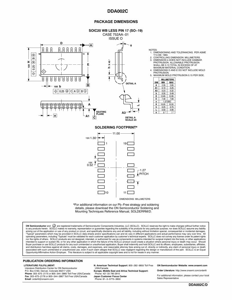
PACKAGE DIMENSIONS
SOIC20 WB LESS PIN 17 (SO−19)CASE 752AA−01
ISSUE O
19
1
11
10
b19X
H10
X
A3
L
A1
A
SEATINGPLANE
�
hX
45�
E
D
M0.
25M
B
M0.25 SA SBC
eC
B
A
DIM MIN MAXMILLIMETERS
A 2.35 2.65A1 0.10 0.25
b 0.35 0.49A3 0.23 0.32
D 12.65 12.95E 7.40 7.60e 1.27 BSCH 10.05 10.55h 0.25 0.75L 0.50 0.90� 0 7
NOTES:1. DIMENSIONING AND TOLERANCING PER ASME
Y14.5M, 1994.2. CONTROLLING DIMENSION: MILLIMETERS.3. DIMENSION b DOES NOT INCLUDE DAMBAR
PROTRUSION. ALLOWABLE PROTRUSIONSHALL BE 0.13 TOTAL IN EXCESS OF ATMAXIMUM MATERIAL CONDITION.
4. DIMENSIONS D AND E DO NOT INCLUDE MOLDPROTRUSION.
5. MAXIMUM MOLD PROTRUSION 0.15 PER SIDE.
� �
DETAIL A
DETAIL ASCALE 2X
11.00
19X0.52
19X 1.30
1.27
DIMENSIONS: MILLIMETERS
1
PITCH
19
10 11
*For additional information on our Pb−Free strategy and solderingdetails, please download the ON Semiconductor Soldering andMounting Techniques Reference Manual, SOLDERRM/D.
SOLDERING FOOTPRINT*
ON Semiconductor and are registered trademarks of Semiconductor Components Industries, LLC (SCILLC). SCILLC reserves the right to make changes without further noticeto any products herein. SCILLC makes no warranty, representation or guarantee regarding the suitability of its products for any particular purpose, nor does SCILLC assume any liabilityarising out of the application or use of any product or circuit, and specifically disclaims any and all liability, including without limitation special, consequential or incidental damages.“Typical” parameters which may be provided in SCILLC data sheets and/or specifications can and do vary in different applications and actual performance may vary over time. Alloperating parameters, including “Typicals” must be validated for each customer application by customer’s technical experts. SCILLC does not convey any license under its patent rightsnor the rights of others. SCILLC products are not designed, intended, or authorized for use as components in systems intended for surgical implant into the body, or other applicationsintended to support or sustain life, or for any other application in which the failure of the SCILLC product could create a situation where personal injury or death may occur. ShouldBuyer purchase or use SCILLC products for any such unintended or unauthorized application, Buyer shall indemnify and hold SCILLC and its officers, employees, subsidiaries, affiliates,and distributors harmless against all claims, costs, damages, and expenses, and reasonable attorney fees arising out of, directly or indirectly, any claim of personal injury or deathassociated with such unintended or unauthorized use, even if such claim alleges that SCILLC was negligent regarding the design or manufacture of the part. SCILLC is an EqualOpportunity/Affirmative Action Employer. This literature is subject to all applicable copyright laws and is not for resale in any manner.
PUBLICATION ORDERING INFORMATIONN. American Technical Support: 800−282−9855 Toll FreeUSA/Canada
Europe, Middle East and Africa Technical Support:Phone: 421 33 790 2910
Japan Customer Focus CenterPhone: 81−3−5773−3850
DDA002C/D
LITERATURE FULFILLMENT:Literature Distribution Center for ON SemiconductorP.O. Box 5163, Denver, Colorado 80217 USAPhone: 303−675−2175 or 800−344−3860 Toll Free USA/CanadaFax: 303−675−2176 or 800−344−3867 Toll Free USA/CanadaEmail: [email protected]
ON Semiconductor Website: www.onsemi.com
Order Literature: http://www.onsemi.com/orderlit
For additional information, please contact your localSales Representative