custom cmos image sensor with multi-channel high-speed readout
TRANSCRIPT

6
Custom CMOS Image Sensor with Multi-Channel High-Speed Readout Dedicated to WDM-SDM
Indoor Optical Wireless LAN
Keiichiro Kagawa Shizuoka University
Japan
1. Introduction
Visually-assisted optical indoor wireless local area network (LAN) is promising not only for high-speed but for offering intuitive user interface. Free-space optical communications (FSOC)(Jahns, 1994) are a key technology to create image-based ultra-fast wireless communication systems of the future. Compared with radio-frequency (RF) electromagnetic waves, the outstanding features of free-space light in terms of wireless communications are two-dimensional imaging with lenses as well as much higher frequency (> 100 THz), spatial and wavelength parallelism, and security. I believe that fusion of imaging and free-space optical communications can dramatically improve usability of indoor wireless LANs (Barry, 1994; O'Brien, 2005; Nonaka, 2006).
I have developed a new indoor optical wireless LAN system (Kagawa, 2003) that can offer a visually-intuitive user interface as well as high-speed data transfer based on two kinds of multiplexing. The key device is a complimentary-metal-oxide- semiconductor (CMOS) image sensor (Fossum, 1997). The device developed can receive several high-frequency amplitude-modulation optical signals at the same time as well as capture ordinary video-rate movies.
The image in the optical wireless LAN can be understood in two ways. One is that it shows the positions of communication nodes or the hub on the scene in a visual manner, which is very intuitive. For example, an actual scene image overlapped with identifiers like icons of communication nodes or the hub will add a feature of location awareness to the normally invisible network. Such interface combining the cyber space with the real will make the computer network more user-friendly. The other understanding of the image is spatial parallelism. Each light source out of the same line of sight is spatially separated on the image, which implies high-speed optical data acquisition by space-division-multiplexing (SDM) optical communications if the fast optical signals incident on different pixels can be read out concurrently.
In the FSOC, chromatic dispersive elements such as a grating are able to convert wavelength-division-multiplexing (WDM) to SDM by decomposing a single WDM light beam to multiple spots on the CMOS image sensor. The dedicated CMOS image sensor enables a fusion of imaging and FSOC, and can enhance the communication bandwidth of indoor wireless networks.
www.intechopen.com

Advanced Wireless LAN
122
In this chapter, preliminary experiments of WDM optical data transmission with the dedicated CMOS image sensor are shown. In Sec. 2, fundamental configurations of the SDM-WDM indoor optical wireless LAN system and the communication modules are described. In Sec. 3, a wide-angle beam steering optics is mentioned. In Sec. 4, preliminary experiments with the dedicated CMOS image sensor and the beam steering optics are shown. Section 5 summarizes this Chapter.
2. SDM-WDM indoor optical wireless LAN
2.1 System configuration
Figure 1 shows a schematic drawing of the proposed space- and wavelength-division-multiplexing (SDM-WDM) indoor optical wireless LAN(Fujiuchi, 2004). The nodes connected to personal computers communicate each other via the hub installed on the ceiling. One of the most significant features of the proposed optical wireless LAN is that dedicated CMOS image sensors are utilized at both of the hub and the nodes as multi-point parallel photoreceivers as well as an image sensor for detecting the positions of communication target(s) on the scene.
Diffusive light
(a position marker)
Dedicated CMOSimage sensor
Node
Node
Narrow beam
膅for comm.䐢
Data output
Video output
Hub
Imaging lens
Light sources(VCSELs)Beam
deflector
Scan lens
DOWNLINK:
WDM communication
UPLINK: concurrent
data acquisition from
multiple nodes
PC-A
PC-B
Fig. 1. SDM-WDM indoor optical wireless LAN using dedicated CMOS image sensors.
The dedicated CMOS image sensors are able to receive multiple optical signals at the different positions on them concurrently. With this ability, SDM can be adopted for the uplinks because the uplinks are multi-to-one connection. On the other hand, the downlinks are physically one-to-one connection between the hub and a node when the hub has only one transmitter. To increase the bandwidth of the downlink, parallelism of the dedicated CMOS image sensor is applied to implement a WDM feature.
The dedicated CMOS image sensor is equipped with two kinds of electric outputs: a movie of scene images and parallel digital output of optical signals. Each pixel operates in one of two functional modes: an image sensor mode and a photoreceiver mode. A communication link is established as follows; Firstly, the functional mode of every pixel is set to the image
www.intechopen.com
Custom CMOS Image Sensor with Multi-Channel High-Speed Readout Dedicated to WDM-SDM Indoor Optical Wireless LAN
123
sensor mode, and each node and the hub emits a diffusive light with a predefined frequency or a sequence as a position marker. After the positions of the nodes and the hub are specified with some image processing, the operation mode of the pixels receiving the optical signals is set to the photoreceiver mode. Then, they begin to emit a narrow beam toward the detected counterpart(s). After the connection is established, the scene image captured at the hub is transferred to the node, and it is displayed with the identifiers of the nodes such as icons superimposed. The network users can recognize where the other communication nodes are in the communication area.
2.2 Communication modules
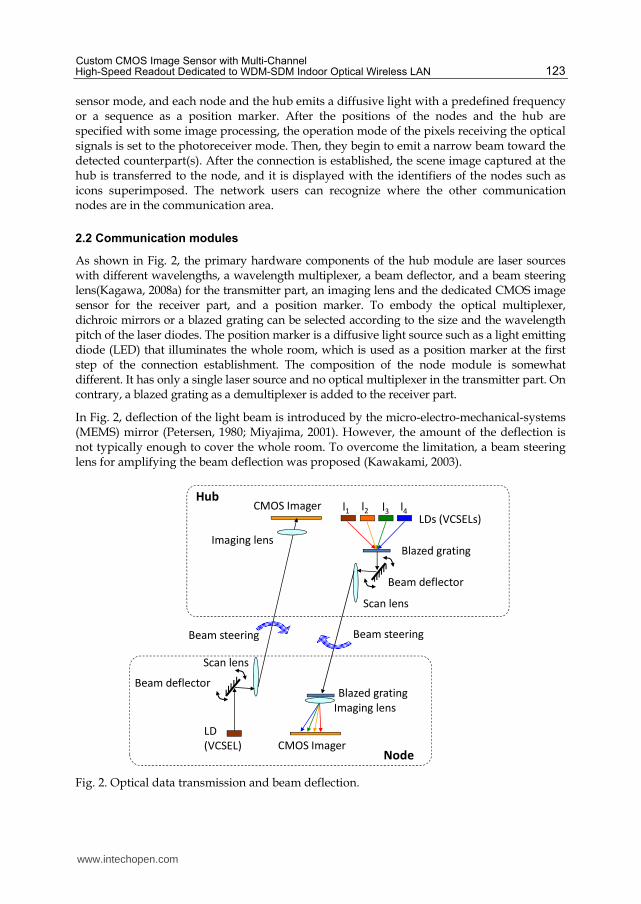
As shown in Fig. 2, the primary hardware components of the hub module are laser sources with different wavelengths, a wavelength multiplexer, a beam deflector, and a beam steering lens(Kagawa, 2008a) for the transmitter part, an imaging lens and the dedicated CMOS image sensor for the receiver part, and a position marker. To embody the optical multiplexer, dichroic mirrors or a blazed grating can be selected according to the size and the wavelength pitch of the laser diodes. The position marker is a diffusive light source such as a light emitting diode (LED) that illuminates the whole room, which is used as a position marker at the first step of the connection establishment. The composition of the node module is somewhat different. It has only a single laser source and no optical multiplexer in the transmitter part. On contrary, a blazed grating as a demultiplexer is added to the receiver part.
In Fig. 2, deflection of the light beam is introduced by the micro-electro-mechanical-systems (MEMS) mirror (Petersen, 1980; Miyajima, 2001). However, the amount of the deflection is not typically enough to cover the whole room. To overcome the limitation, a beam steering lens for amplifying the beam deflection was proposed (Kawakami, 2003).
Node
Hubl1 l2 l3 l4CMOS Imager
LDs (VCSELs)
LD
(VCSEL)
Blazed grating
Blazed grating
Beam deflector
Scan lens
Beam steering
Imaging lens
Imaging lens
Beam deflector
Scan lens
Beam steering
CMOS Imager
Fig. 2. Optical data transmission and beam deflection.
www.intechopen.com

Advanced Wireless LAN
124
3. Dedicated CMOS image sensor
3.1 Sensor architecture
The CMOS image sensor dedicated to the proposed SDM-WDM indoor optical wireless LAN is a fusion of an ordinary image sensor and an array of photoreceiver circuits used in optical fiber communications. Figure 3 shows a block diagram of the dedicated CMOS image sensor. The pixel array is composed of NX×NY pixels, and the sensor has NC parallel photoreceivers and data output channels. All signals for the communication are fully differential. For the image sensor mode, the image readout circuits are prepared at the top of the pixel array. The circuits below the pixel array are for the photoreceiver mode, which are composed of transimpedance amplifiers (TIA) with offset cancellation current sources controlled by automatic offset cancellers (AOCs) post amplifiers, bus drivers, an analog multiplexer to select NC outputs out of NX columns, bus receivers, a crosstalk reduction matrix operator, limiters to binarize the amplified photo-signals, and open-drain buffers.
Pixel array
(NX×NY)
A/D converter
X decoder
NX TIAs
NX post-amplifiers
NX×NC-
analog multiplexer
NC-ch
cross-talk reduction
(matrix operator)
NC
limiters
Gain
control of
TIA
NC output
buffers
NC-ch high-speed data outputs
Image output
NX bus driver
Multiplexer X decoder
Fig. 3. Sensor architecture.
3.2 Pixel
3.2.1 Circuits
To implement the multi-point optical data acquisition function, each pixel has digital control logic to change its behaviour according to the operation mode (Fig. 4). For the signal
www.intechopen.com

Custom CMOS Image Sensor with Multi-Channel High-Speed Readout Dedicated to WDM-SDM Indoor Optical Wireless LAN
125
readout, pixel<i, j> has two kinds of output signal lines: one analog image output line (Vaps<i>) and two differential analog photocurrent output lines (Vsig<i-1>, Vref<i-1>, Vsig<i>, and Vref<i>) in the both sides of the pixel, which are selected by MEM_L<i, j> and MEM_R<i, j>. Note that <i, j> denotes the pixel position. xs<i> and ys<j> are horizontal and vertical addressing signals. rr<j> and rs<j> are row reset and select signals, respectively.
QDG
QDG
rs<j>rr<j>ys<j>
xs<
i>
Vsi
g<
i-1
>V
ref<
i-1>
Vsi
g<
i>V
ref<
i>
Vaps<
i>
MS_L MS_R
Pixel<i+1,j>
Pixel<i-1,j>
MEM_L<i,j> MEM_R<i,j>
MEM_R<i+1,j>
MEM_L<i-1,j>
Vref<i-2,j>
Vref<i+1,j>
Pixel<i-1,j> Pixel<i+1,j>
Pixel<i-2,j>
Pixel<i+2,j>
Fig. 4. Pixel circuits.
For the signal readout, the pixel has two kinds of output signals as mentioned above. The differences between two operation modes are detection schemes of the optical signal. In the
image sensor mode, photocurrent is accumulated at the photodiode so that extremely high
photosensitivity is achieved but its speed is very slow (up to around several MHz). In the photoreceiver mode, the photocurrent is directly put out to the TIA and amplified. In the
photoreceiver mode, the photocurrent is directly amplified by the TIA prepared for each column without accumulation. Therefore, it can detect high-frequency signals but has low
sensitivity. These complementary features are suited to detect the dim marker light in the imager mode and the strong narrow beam for communication in the photoreceiver mode.
3.2.2 Dynamic pixel reconfiguration for fully differential signaling
Another important feature of the pixel is dynamic differential reconfiguration to work as either a reference or a signal pixel. Without this feature, we cannot receive photo signals while capturing images because many kinds of noise sources on the CMOS image sensor and the print circuit board significantly decrease the signal integrity of the photoreciever circuits. While optical signals are amplified with capturing images, image readout digital circuitry becomes noise sources. Such common-mode noise can be suppressed by
www.intechopen.com

Advanced Wireless LAN
126
differential signalling. However, fully differential configuration needs replica pixels to put out the reference signal, which increases the pixel area (Zimmerman, 2003).
Figure 5 shows the schematic of the dynamic differential reconfiguration. In the figure, 2×2 pixels receiving optical signals work as a signal pixel, and four pixels in their both sides work as a reference pixel. With this method, differential signalling can be realized without replica pixels
Communication light spot
Signal output Reference output
Ref
Ref Ref
RefSig
Sig Sig
Sig
Fig. 5. Dynamic pixel reconfiguration.
3.3 Prototype sensor
Table 1 and Fig. 6 show specifications and a photograph of the dedicated CMOS image sensor. To build a demonstration system, photosensitivity of the CMOS image sensor should be high. Therefore, a high-sensitive but slow photodiode comprised of an N-well/ P-substrate-junction diode was selected. The bandwidth of the photo-amplifier was designed to be comparable with that of the photodiode. Figure 7 and Table 2 show a prototype board and specifications of an advanced version of the dedicated CMOS image sensor fabricated in a 0.18-┤m CMOS technology. This chip has not been fully tested.
Technology 0.35-┤m CMOS 2-poly, 3-metal
Chip size 9.8 mm sq.
Pixel count 64 x 64
Pixel size 100 ┤m sq.
Photodiode structure N-well/ P-substrate
Fill factor 16% (no microlens)
Photoamplifier Regulated cascode amp (TIA)/ Cherry-Hooper amp
(post amp and gain stage)
Total transimpedance gain 2.5 kΩ – 2.5 MΩ (simulation)
Bandwidth 7.9 MHz (simulation)
Number of channels 4
Table 1. Specifications of the CMOS image sensor.
www.intechopen.com

Custom CMOS Image Sensor with Multi-Channel High-Speed Readout Dedicated to WDM-SDM Indoor Optical Wireless LAN
127
Fig. 6. Photograph of the prototype CMOS image sensor.
Fig. 7. Prototype board for CMOS image sensor in a 0.18-┤m CMOS technology.
Technology 0.18-┤m CMOS 1-poly, 5-metal
Pixel count 180×84
Pixel size 31.25 ┤m×62.50 ┤m
Photodiode structure Deep N-well/ P-well
Fill factor 20%
Communication channels 4
Data rate >1.0Gbps/ch (simulation)
Table 2. Specifications of the CMOS image sensor in a 0.18-┤m CMOS technology.
www.intechopen.com

Advanced Wireless LAN
128
4. Wide-angle beam steering optics
4.1 Optical setup
The task of the optical transmitter is to deliver a narrow laser beam for communication to anywhere in the whole room with a size of more than 5 m by 5 m. For this purpose, a beam steering optics shown in Fig. 8 is proposed. The optical system is composed of three parts: a wavelength multiplexer, a beam deflector, and a beam-deflection-angle enhancer. The feature of the system is that the beam deflection enhancer is inserted at the exit of the beam steering optics to realize a compact and wide-angle optical transmitter.
To combine laser beams with wavelengths of ┣1-┣4 into a single beam, the following equation should be satisfied. Note that δ, Δ┣, d, and f1 are the pitch and the wavelength difference of the adjacent lasers, the pitch of the blazed grating, and the focal length of lens, L1.
.1fd
(1)
Because the availability of the MEMS mirror satisfying the requirements for the optical transmitter is not always good, the beam deflection part is implemented by a combination of a focusing lens (L2) on a compact two-dimensional stage and a collimator lens (L3). The focusing lens, L2, moves in the plane perpendicular to the optical axis. In this setup, an intermediate image is generated at the relayed image position in Fig. 8. When the displacement of L2 in one axis is represented by Δ, the output angle of the beam from L3, θIN, is written by
13Tan ,IN f (2)
where f3 means the focal length of L3. The beam steering lens as the beam deflection enhancer amplifies the input angle of the collimated beam, θIN, with a certain angle gain to obtain the large output angle, θOUT. With the beam steering lens, a wide range of the beam deflection angle can be achieved for a small displacement of L2.
Light source (VCSEL)
f1 f2 f3
f1 f2 f3
Δ
Deflectionenhancer
L1 L2 L3
INOUT
Relayed image position
δ
λ1
λ2 λ3
λ4
Wavelength multiplexer
Beam deflector
Beam steering lens
Fig. 8. Optical setup of wide-angle beam steerer.
www.intechopen.com

Custom CMOS Image Sensor with Multi-Channel High-Speed Readout Dedicated to WDM-SDM Indoor Optical Wireless LAN
129
4.2 Beam steering lens
The beam steering lens has a reverse-telephoto-type configuration (Smith, 2000). A prototype lens whose structure and specifications shown in Fig. 9 and Table 3, respectively, were designed and fabricated (Miyawaki, 2007; Kagawa, 2008a). The lens is designed for wavelengths of an 850-nm band, and its maximum field of view is 140-degree. The maximum gain of the beam angle is 3.5. A ray diagram is shown in Fig. 10. Because the left surface of the rear lens has a large curvature, the rear lens is composed of aspherical surfaces to minimize the output beam distortion. The feature of this beam steering lens is large tolerance of the alignment along the optical axis due to its infinite conjugate design, which makes assembly easier.
10.8 mm
Input
Fig. 9. Configuration of the beam steering lens.
Wavelength 845-851 nm
Focal length 2.1 mm
Field of view 140 degree (max)
Overall length after assembly 10.2 mm
Working distance 5.0 mm
Acceptable input beam diameter 1.0 mm
Effective output diameter 10 mm
Beam angle gain 3.5 (max)
Material K-SFLD6 (front),PBK40 (rear)
Table 3. Specifications of the beam steering lens.
Aspherical lens
Spherical lens
K-SFLD6
PBK40
Light
source
Collimator
lens
Rotating mirror
Fig. 10. Ray diagram.
www.intechopen.com

Advanced Wireless LAN
130
4.3 Prototypes
A mounted lens is shown in Fig. 11. With this lens, the beam steering optics shown in Fig. 8 was constructed (Fig. 12). For simplicity, WDM was not implemented in this prototype. A laterally-single-mode GaAs vertical-cavity surface-emitting laser (VCSEL) was used as a laser source (FujiXerox, Model VCSEL-AS-0001, wavelength of 840-860 nm, maximum beam divergence of 20 degrees (FWHM), optical output power of 2 mW). The focusing lens, L2, was mounted on a movable compact stage (mechOnics, Model MS15, travel of 3.5 mm, maximum speed of 1.5 mm/s). f3 was set to 2.2 mm. For this configuration, Δ should should range between about ±0.8 mm.
(Unit: cm)
Fig. 11. Beam steering lens.
Beam deflector
Beam steering lens
VCSEL
Collimator lens
Fig. 12. Prototype of beam steerer.
www.intechopen.com

Custom CMOS Image Sensor with Multi-Channel High-Speed Readout Dedicated to WDM-SDM Indoor Optical Wireless LAN
131
5. Experiments
5.1 SDM data transfer
Figure 13 shows an experimental setup for uplink. The receiver of the hub was installed on the ceiling, and two transmitters ware placed on a desk. The vertical distance between the hub and the node was about 1.75 m. Transmitted data were generated by the data generator (Model DG2030, Tektronix, four digital output channels, data rate of 400Mbps per channel). For electric-to-optic (E/O) conversion, E/O converters (Model LL-650GI (┣=650 nm), LL-780GI (┣=780 nm), LL-900GI (┣=900nm), Graviton Inc., bandwidth of 1.2GHz) were used. The dedicated CMOS image sensor was controlled by a field-programmable gate array (FPGA). Control commands such as "start" or "stop image capturing", "set the pixels in the photoreceiver mode", and "set all the pixels in the image sensor mode" were issued by a personal computer through serial communication interface. An analog signal of the video output from the CMOS image sensor was converted to 10-bit digital value by an analog-to-digital conversion (ADC) chip. Then, it was transferred to the personal computer through a 10-bit parallel digital input-output (I/O).
1.75 m
Hub
Node
Fig. 13. Experimental setup for SDM data transfer.
Figure 14(a) shows a scene image captured at the hub when all pixels operated in the image sensor mode. A video lens (TECH SPEC, focal length of 4.3 mm, F/1.8) was used. Two regions indicated by the arrows in the figure are transmitters on the desk. Then, the operation mode of these pixels was set to the photoreceiver mode. Due to the dynamic reconfiguration, 4×2 pixels for each region became white. It is because these pixels are biased by the TIAs to amplify the photocurrent directly. The optical power before the imaging lens was about 200 ┤W.
www.intechopen.com

Advanced Wireless LAN
132
(a)
(b)
Transmitters
Fig. 14. Captured images for (a) all pixels in image sensor mode and (b) two rectangles in photoreceiver mode.
Figure 15 shows eye diagrams for the two nodes while images were being captured. The data rate was 10 Mbps/channel. This result shows that common-mode noise from the digital circuits on the CMOS image sensor to the photoreceiver circuits was well suppressed. The data rates were the same, but the wavelengths were different; for channel-1 and -2, the wavelengths were 780 nm and 650 nm, respectively. The delay becomes larger as the wavelength becomes longer. The differences of rise and fall times in the waveforms reflect dependency of the delay of the diffusion carriers generated in the silicon substrate of the CMOS image sensor on the wavelength. In the results shown in Ref. (Kagawa, 2008b) without differential signalling, the signal to crosstalk ratio (SCR), defined as the signal saturation level relative to peak-to-peak crosstalk, was 2.2 dB. With the full-differentiation technique, the SCR was about 11dB and 18dB for one of the differential pair and after subtraction, respectively.
Ch#1
Ch#2
Clock
Fig. 15. Eye diagrams for the two nodes.
www.intechopen.com
Custom CMOS Image Sensor with Multi-Channel High-Speed Readout Dedicated to WDM-SDM Indoor Optical Wireless LAN
133
5.2 WDM data transfer
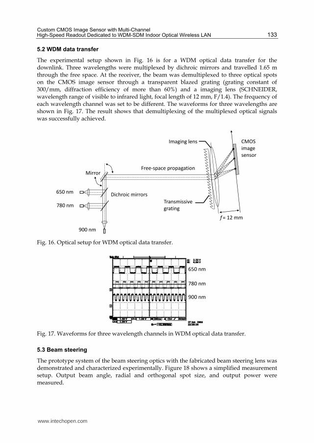
The experimental setup shown in Fig. 16 is for a WDM optical data transfer for the downlink. Three wavelengths were multiplexed by dichroic mirrors and travelled 1.65 m through the free space. At the receiver, the beam was demultiplexed to three optical spots on the CMOS image sensor through a transparent blazed grating (grating constant of 300/mm, diffraction efficiency of more than 60%) and a imaging lens (SCHNEIDER, wavelength range of visible to infrared light, focal length of 12 mm, F/1.4). The frequency of each wavelength channel was set to be different. The waveforms for three wavelengths are shown in Fig. 17. The result shows that demultiplexing of the multiplexed optical signals was successfully achieved.
CMOS
image
sensor
Transmissive
grating
900 nm
780 nm
650 nm
f= 12 mm
Imaging lens
Mirror
Dichroic mirrors
Free-space propagation
Fig. 16. Optical setup for WDM optical data transfer.
650 nm
780 nm
900 nm
Fig. 17. Waveforms for three wavelength channels in WDM optical data transfer.
5.3 Beam steering
The prototype system of the beam steering optics with the fabricated beam steering lens was demonstrated and characterized experimentally. Figure 18 shows a simplified measurement setup. Output beam angle, radial and orthogonal spot size, and output power were measured.
www.intechopen.com

Advanced Wireless LAN
134
Optical transmitter
Screen
Radial Orthogonal
Output beam angle
Fig. 18. Configuration for characterizing the beam steering lens.
Figure 19(a) shows a measured relationship between the input and the output beam angles of the beam steering lens. The maximum output beam angle was about 66 degrees in the experiments, which was large enough to cover a 5 m-by-5 m room when the vertical distance between the hub and a node was larger than 2 m. The maximum angle gain was 3.4, which showed a good agreement with the design.
0
10
20
30
40
50
60
70
0 5 10 15 20
Ou
tpu
t bea
m a
ng
le[d
eg]
Input beam angle [deg]
0
10
20
30
40
50
60
70
80
0 10 20 30 40 50 60 70
Bea
m s
ize
[mm
]
Output beam angle [deg]
Radial
Orthogonal
0.5
0.6
0.7
0.8
0.9
1
0 10 20 30 40 50 60 70
Eff
icie
ncy
Output beam angle [deg]
(a) (b)
(c)
Fig. 19. Experimental results of the scan lens: (a) relationship between input and output beam angles, (b) beam sizes on the ceiling, and (c) power efficiency.
www.intechopen.com

Custom CMOS Image Sensor with Multi-Channel High-Speed Readout Dedicated to WDM-SDM Indoor Optical Wireless LAN
135
The beam size on the receiver plane is a significant concern because it defines received power, namely, the signal integrity. The beam size strongly depends on the radiation angle and the size of the laser source. Figure 19(b) shows the beam sizes measured on the ceiling 173 cm above the beam steering optics. The radial beam size increases as the output beam angle becomes large.
Figure 19(c) shows the optical power efficiencies of the beam steering lens. The minimum efficiency at the maximum output beam angle was bout 0.8 (-2dB). Note that the sidelobes of the beam were included in the measured power, and the actual efficiencies were possibly smaller than the results in Fig. 19(c).When we assume that the received optical power is in proportion to the beam area, the optical power variation at the receiver introduced by the beam steering optics is about 13dB, which can be tolerated by the dedicated CMOS imager by a gain control of the photoreceiver circuits. In conclusion, the experimental results showed that the prototype beam steering optics operated successfully.
6. Conclusion
A space- and wavelength-division-multiplexing (SDM and WDM) indoor optical wireless LAN system, which is based on a dedicated CMOS image sensor to realize a compact, high-speed, and intelligent nodes and hub, was described. The dedicated CMOS image sensor can detect multiple fast optical data concurrently as well as captures ordinary images from which positions of communication nodes or the hub is obtained. In this Chapter, with the CMOS image sensor, an application of WDM technique to downlinks was demonstrated. 64x64-pixel custom CMOS image sensor with 4-channel concurrent data acquisition function was fabricated. Experimental results showed that the CMOS sensor received 10Mbps x 3ch WDM data while capturing ordinary images. A wide-angle beam steering optics with a beam steering lens for amplifying the output beam angle was demonstrated. A prototype beam steering lens optimized for a near-infrared wavelength of 850 nm was fabricated. Experimental results showed that the maximum output beam angle was about ±60 degrees, which was enabled to cover a 5m-by-5m room (for the ceiling 2.0 m above the nodes), and the optical power efficiency was larger than 0.8. The received optical power variation caused by the power efficiency fluctuation and the beam distortion was roughly estimated to be 13dB, which was tolerated by the dedicated CMOS imager.
7. Acknowledgment
This research was promoted by Strategic Information and Communications R&D Promotion Program (SCOPE) by Ministry of Internal Affairs and Communications, and was partially supported by “Global COE (Centers of Excellence) Program” of the Ministry of Education, Culture, Sports, Science and Technology, Japan. This work was also supported by VLSI Design and Education Center(VDEC), the University of Tokyo in collaboration with Cadence Design Systems, Inc. The VLSI chips in this study were fabricated in the chip fabrication program of VLSI Design and Education Center (VDEC), the University of Tokyo in collaboration with Rohm Corporation and Toppan Printing Corporation.
I am grateful to Jun Ohta at Nara Institute of Science and Technology (NAIST) for valuable advice, and to Eiji Tanaka at Panasonic Electronic Devices Co., Ltd. for kindly supporting design and fabrication of the beam steering lens. I would like to heartily appreciate tremendous devotions of the students at NAIST who were involved in this study.
www.intechopen.com

Advanced Wireless LAN
136
8. References
Jahns, J. (1994). Optical computing hardware, Academic Press, ISBN 978-012-3799-95-1, Boston, USA.
Barry, J. R. (1994). Wireless Infrared Communications, Kluwer Academic Publishers, ISBN 978-079-2394-76-1, Norwell, UK.
O’Brien, D. C.; Faulkner, G. E.; Zyambo, E. B.; Jim, K.; Edwards, D.; Stavrinou, P.; Parry, G.; Bellon, J.; Sibley, M. J.; Lalithambika, V. A.; Joyner, V. M.; Samsudin, R. J.; Holburn, D. M.; Mears, R. J. (2005). Integrated transceivers for optical wireless communications, IEEE J. Sel. Top. in Quantum Electron., Vol. 11, No. 1, pp. 173-183.
Nonaka, K.; Isobe, Y.; Tachibana, M. (2006). Optical Micro-cell System: Smart Optical Wireless Access Data-Communication for Moving User Terminals, Jpn. J. Appl. Phys., Vol. 45, pp. 6762-6766.
Kagawa, K.; Nishimura, T.; Hirai, T.; Yamasaki, Y.; Ohta, J.; Nunoshita, M.; Watanabe, K. (2003). Proposal and preliminary experiments of indoor optical wireless LAN based on a CMOS image sensor with a high-speed readout function enabling a low-power compact module with large uplink capacity, IEICE Trans. Comm., Vol. E86-B, No. 5, pp. 1498-1507.
Fossum, E. R. (1997). CMOS image sensors: electronic camera-on-a-chip, IEEE Trans. Electron. Devices, Vol. 44, No.10, pp. 1689-1698.
Fujiuchi, A.; Ikeuchi, T.; Kagawa, K.; Ohta, J.; Nunoshita, M. (2004). Free-space wavelength-division-multiplexing optical communications using a multi-channel photoreceiver, Proc. of Int'l Conf. Optics & Photonics in Technology Frontier (ICO), pp. 480-481.
Kagawa, K.; Miyawaki, T.; Ohta, J.; Nunoshita, M.; Tanida, J. (2008a). Wide-angle beam scan lens for indoor wireless optical LAN, Proc. of 6th Int’l Conf. on Optics-photonics Design and Fabrication (ODF’08), pp. 297-298.
Petersen, K. E. (1980). Silicon torsional scanning mirror, IBM J. Res. Dev., Vol. 24, No. 5, pp. 631-637.
Miyajima, H.; Asaoka, N.; Arima, M.; Minamoto, Y.; Murakami, K.; Tokuda, K.; Matsumoto, K. (2001). A durable, shock-resistant electromagnetic optical scanner with polyimide-based hinges, J. Microelectromechanical Systems, Vol. 10, No. 3, pp. 418-424.
Kawakami, T.; Kagawa, K.; Nishimura, T.; Asazu, H.; Ohta, J.; Nunoshita, M.; Watanabe, K. (2003). Design of a two-dimensional scan lens for infrared wireless communications and its application to establishing a data path, Proc. of 28th Kogaku Symposium, Tokyo, Japan, pp. 101-102.
Zimmerman, H. (2003). Integrated Silicon Optoelectronics, ISBN 978-354-0666-62-2 Chapter 12, Springer, New York, USA.
Smith, W. J. (2000). Modern optical engineering 3rd edition, SPIE Press, McGraw-Hill, New York, USA, pp. 468-470.
Miyawaki, T.; Kagawa, K.; Tanaka, E.; Yamagata, M.; Tanaka, Y.; Nunoshita, M.; Ohta J. (2007). A wide-angle beam steering lens for 850-nm-band wavelength-multiplexed indoor optical wireless LAN, Proc. of Optics & Photonics Japan 2007, Osaka, Japan, pp. 410-411 (in Japanese).
Kagawa, K; Asazu, H; Nunoshita, M; Ohta. J (2008b). A vision chip with column-level amplification of optical data signals for indoor optical wireless local area networks, Opt. Rev., Vol. 15, No. 1, pp. 1-5.
www.intechopen.com

Advanced Wireless LANEdited by Dr. Song Guo
ISBN 978-953-51-0645-6Hard cover, 136 pagesPublisher InTechPublished online 05, June, 2012Published in print edition June, 2012
InTech EuropeUniversity Campus STeP Ri Slavka Krautzeka 83/A 51000 Rijeka, Croatia Phone: +385 (51) 770 447 Fax: +385 (51) 686 166www.intechopen.com
InTech ChinaUnit 405, Office Block, Hotel Equatorial Shanghai No.65, Yan An Road (West), Shanghai, 200040, China
Phone: +86-21-62489820 Fax: +86-21-62489821
The past two decades have witnessed starling advances in wireless LAN technologies that were stimulated byits increasing popularity in the home due to ease of installation, and in commercial complexes offering wirelessaccess to their customers. This book presents some of the latest development status of wireless LAN, coveringthe topics on physical layer, MAC layer, QoS and systems. It provides an opportunity for both practitioners andresearchers to explore the problems that arise in the rapidly developed technologies in wireless LAN.
How to referenceIn order to correctly reference this scholarly work, feel free to copy and paste the following:
Keiichiro Kagawa (2012). Custom CMOS Image Sensor with Multi-Channel High-Speed Readout Dedicated toWDM-SDM Indoor Optical Wireless LAN, Advanced Wireless LAN, Dr. Song Guo (Ed.), ISBN: 978-953-51-0645-6, InTech, Available from: http://www.intechopen.com/books/advanced-wireless-lan/custom-cmos-image-sensor-with-multi-channel-high-speed-readout-dedicated-to-wdm-sdm-indoor-optic

© 2012 The Author(s). Licensee IntechOpen. This is an open access articledistributed under the terms of the Creative Commons Attribution 3.0License, which permits unrestricted use, distribution, and reproduction inany medium, provided the original work is properly cited.