cs61cl machine structures lec 8 – state and register transfers david culler electrical engineering...
Post on 22-Dec-2015
215 views
TRANSCRIPT

CS61CL Machine Structures
Lec 8 – State and Register Transfers
David CullerElectrical Engineering and Computer Sciences
University of California, Berkeley

CS61CL Road Map
10/14/09 CS61CL F09 2
Hardware
Software
Machine Lang. pgm
Instruction Set Architecture
Machine Organization
HLL Program Asm Lang. Pgm
Co
mp
iler
Ass
emb
ler
foo.cfoo.s
foo.o
I/O systemInstr. Set Proc.
Digital Design
Circuit Design
Datapath & Control
Layout & fab
Semiconductor Materials
foo.exe
Lin
ker

Review: Combinational Logic• Any boolean function can be expressed as an acyclic connection of gates
• Often specified by a truth table
• Outputs are purely a function of the inputs– no history, no state
10/14/09 CS61CL F09 3
Combinational
Logic
inp
uts
ou
tpu
ts
inputs outputs
k
2k

Examples: Logical Operations
10/14/09 CS61CL F09 4
C = A & B
A B
C
A31 B31
C31
A30 B30
C30
A0 B0
C0
°°°
A31:0 B31:0
C31:0
A31:0 B31:0
C31:0
A31:0 B31:0
C31:0
A31:0
C31:0

Example: Multiplexor
10/14/09 CS61CL F09 5
C = S ? A : B
A B
C
S
C = (S & A) | (~S & B)
S
A31:0 B31:0
C31:0

Example: Adder
10/14/09 CS61CL F09 6
A B Ci
Co S
A B Ci
Co S
A B Ci
Co S
A B Ci
Co S
A B Ci
Co S
A31:0 B31:0
C31:0

Example: Arithmetic Logic Unit
10/14/09 CS61CL F09 7
A31:0 B31:0
C31:0
S1:0

ALU
10/14/09 CS61CL F09 8
10/14/09 CS61CL F09 9
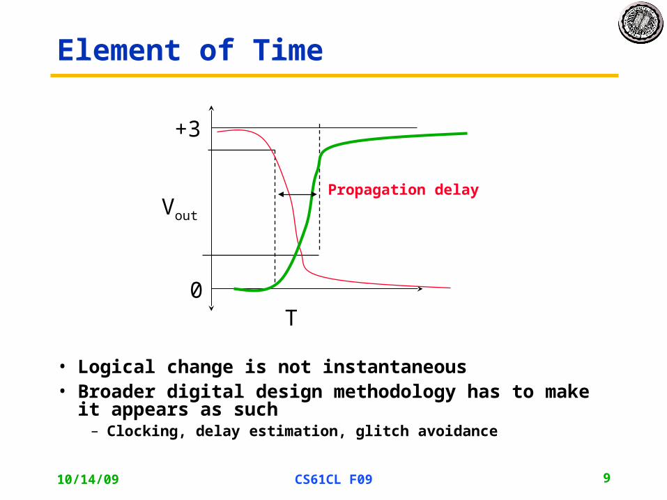
Element of Time
• Logical change is not instantaneous• Broader digital design methodology has to make it appears
as such– Clocking, delay estimation, glitch avoidance
Vout
+3
0T
Propagation delay

10/14/09 CS61CL F09 10
What makes Digital Systems tick?
Combinational
Logic
time
clk
Administrative Issues
• HW 6 due tonight
• Project 2 dues Monday 10/26– bimodal check-off
– testing tools available tomorrow
– they are really picky
• Project 1 grading almost done– Friday
• HW 7 – discuss
• Midterm 2 on 11/9 as in original schedule– 11/11 is holiday
10/14/09 CS61CL F09 11

8/30/2007 12
A Bit of state: D-type edge-triggered flip-flop
• The edge of the clock is used to sample the "D" input & send it to "Q” (positive edge triggering).
– At all other times the output Q is independent of the input D (just stores previously sampled value).
– The input must be stable for a short time before the clock edge.
01 01 010

9/18/07
13
R S R S R S
D Q D Q D Q D Q
OUT1 OUT2 OUT3 OUT4
CLK
IN1 IN2 IN3 IN4
R S
"0"
Registers
• Collections of flip-flops with similar controls and logic– Stored values somehow related (e.g., form binary value)
– Share clock, reset, and set lines
– Similar logic at each stage

What “registers” do we need?
• “read” vs use the output
• “write” on the clock edge => Load
• Load Control
10/14/09 CS61CL F09 14
0r0r1°°°r31PClohi
Programmable storage
2^32 x bytes
31 x 32-bit GPRs (R0=0)
32 x 32-bit FP regs (paired DP)
HI, LO, PC
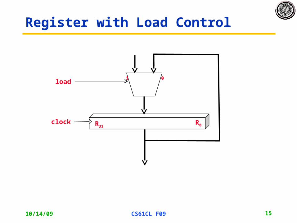
Register with Load Control
10/14/09 CS61CL F09 15
R0R31clock
load1 0

Register File
10/14/09 CS61CL F09 16
R0
°°°
R1
R2
R31
AselBsel
BoutAout
Dsel
1
ld
Dinde
code
r
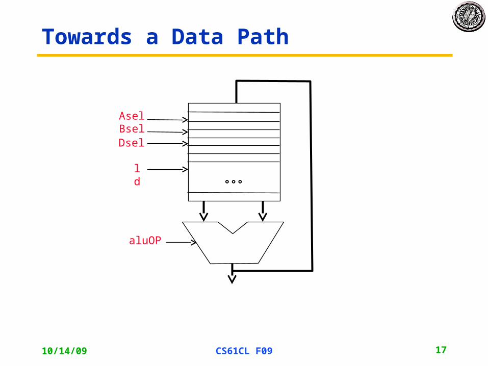
Towards a Data Path
10/14/09 CS61CL F09 17
°°°
AselBselDsel
ld
aluOP

Exercise a Data Path
10/14/09 CS61CL F09 18
°°°
AselBselDsel
ld
aluOP
7
3
24
2
1
7 3
10
10
10 3
13
13
13 3
16

What about RAM - Randomly Accessed Memory?
• Like a HUGE register file– dense, slower, low-cost storage cell (6T)– fewer ports– wider address lines– accessed over a “bus”
• Bus: means of composition in hardware system– logically related collection of wires– interfacing one or more sources to one or more destinations
10/14/09 CS61CL F09 19
RAM
data
address

Recall: Instruction Cycle
9/16/09 UCB CS61CL F09 Lec 4 20
°°°
000..0:
FFF..F:
n:
0B20
0B20:
Instruction Fetch
Execute
PC
32 2 3 1
“add $1,$2,$3”40
61101Operand
Result
Next
Decode
+
0B24
main:

Register Transfers
10/14/09 CS61CL F09 21

10/14/09 CS61CL F09 22
Synchronous Circuit Design
• clock– distributed to all flip-flops
• ALL CYCLES GO THROUGH A REG!
• Combinational Logic Blocks (CL)– Acyclic
– no internal state (no feedback)
– output only a function of inputs
• Registers (reg)– collections of flip-flops
reg regCL CL
clock input
output
option feedback
input output