cs 152 computer architecture and engineeringcs152/sp14/lecnotes/lec12-1.pdf · cs 152 computer...
TRANSCRIPT

UC Regents Spring 2014 © UCBCS 152 L20: Dynamic Scheduling III
2014-4-8John Lazzaro
(not a prof - “John” is always OK)
CS 152Computer Architecture and Engineering
www-inst.eecs.berkeley.edu/~cs152/
TA: Eric Love
Lecture 20 -- Dynamic Scheduling III
Play:1Tuesday, April 8, 14

UC Regents Fall 2006 © UCBCS 152 L20: Dynamic Scheduling III
Intel Inside: Dynamic Execution
The IA-32 ISA: How to adapt a complex instruction set to dynamic techniques.
Limits to Parallelism: How fast can the perfect dynamic execution design go?
Sandy Bridge: Dynamic execution in today’s Core and Xeon product lines.
Short Break
Pentium IV: Case study of the Netburst micro-architecture, introduced in 2001.
2Tuesday, April 8, 14
3-1 0 Vol. 1
BASIC EXECUTION ENVIRONMENT
• General-purpose registers. These eight registers are available for storing operands and pointers.
• Segment registers. These registers hold up to six segment selectors.
• EFLAGS (program status and control) register. The EFLAGS register report on the status of the program being executed and allows limited (application-program level) control of the processor.
• EIP (instruction pointer) register. The EIP register contains a 32-bit pointer to the next instruction to be executed.
3.4.1 General-Purpose RegistersThe 32-bit general-purpose registers EAX, EBX, ECX, EDX, ESI, EDI, EBP, and ESP are provided for holding the following items:
• Operands for logical and arithmetic operations
• Operands for address calculations
• Memory pointers
Although all of these registers are available for general storage of operands, results, and pointers, caution should be used when referencing the ESP register. The ESP register holds the stack pointer and as a general rule should not be used for another purpose.
Many instructions assign specific registers to hold operands. For example, string instructions use the contents of the ECX, ESI, and EDI registers as operands. When using a segmented memory model, some instructions assume that pointers in certain registers are relative to specific segments. For instance, some instructions assume that a pointer in the EBX register points to a memory location in the DS segment.
Figure 3-4. General System and Application Programming Registers
03 1EAXEBXECXEDXESIEDIEBPESP
Segment Regist ers
CSDSSSESFSGS
01 5
03 1EFLAGS
EIP3 1 0
General-Purpose Regist ers
Program Status and Control Regist er
Instruction Point er3-1 0 Vol. 1
BASIC EXECUTION ENVIRONMENT
• General-purpose registers. These eight registers are available for storing operands and pointers.
• Segment registers. These registers hold up to six segment selectors.
• EFLAGS (program status and control) register. The EFLAGS register report on the status of the program being executed and allows limited (application-program level) control of the processor.
• EIP (instruction pointer) register. The EIP register contains a 32-bit pointer to the next instruction to be executed.
3.4.1 General-Purpose RegistersThe 32-bit general-purpose registers EAX, EBX, ECX, EDX, ESI, EDI, EBP, and ESP are provided for holding the following items:
• Operands for logical and arithmetic operations
• Operands for address calculations
• Memory pointers
Although all of these registers are available for general storage of operands, results, and pointers, caution should be used when referencing the ESP register. The ESP register holds the stack pointer and as a general rule should not be used for another purpose.
Many instructions assign specific registers to hold operands. For example, string instructions use the contents of the ECX, ESI, and EDI registers as operands. When using a segmented memory model, some instructions assume that pointers in certain registers are relative to specific segments. For instance, some instructions assume that a pointer in the EBX register points to a memory location in the DS segment.
Figure 3-4. General System and Application Programming Registers
03 1EAXEBXECXEDXESIEDIEBPESP
Segment Regist ers
CSDSSSESFSGS
01 5
03 1EFLAGS
EIP3 1 0
General-Purpose Regist ers
Program Status and Control Regist er
Instruction Point er
Vol. 1 3-7
BASIC EXECUTION ENVIRONMENT
3.3.2 Paging and Virtual MemoryWith the flat or the segmented memory model, linear address space is mapped into the processor’s physical address space either directly or through paging. When using direct mapping (paging disabled), each linear address has a one-to-one correspondence with a physical address. Linear addresses are sent out on the processor’s address lines without translation.
When using the IA-32 architecture’s paging mechanism (paging enabled), linear address space is divided into pages which are mapped to virtual memory. The pages of virtual memory are then mapped as needed into physical memory. When an operating system or executive uses paging, the paging mechanism is transparent to an applica-tion program. All that the application sees is linear address space.
In addition, IA-32 architecture’s paging mechanism includes extensions that support:
• Physical Address Extensions (PAE) to address physical address space greater than 4 GBytes.
• Page Size Extensions (PSE) to map linear address to physical address in 4-MBytes pages.
See also: Chapter 3, “Protected-Mode Memory Management,” in the Intel® 64 and IA-32 Architectures Software Developer’s Manual, Volume 3A.
3.3.3 Memory Organization in 64-Bit ModeIntel 64 architecture supports physical address space greater than 64 GBytes; the actual physical address size of IA-32 processors is implementation specific. In 64-bit mode, there is architectural support for 64-bit linear address space. However, processors supporting Intel 64 architecture may implement less than 64-bits (see Section 3.3.7.1). The linear address space is mapped into the processor physical address space through the PAE paging mechanism.
Figure 3-3. Three Memory Management Models
Linear Address
Flat Model
LinearAddress
Space*
Segment Selector
Of fset
Segment Selector
Segmented Model
Real-Address Mode Model
Linear Address
Logical
Of fset (ef fective address)
Space DividedInto Equal
Sized SegmentsAddress
LogicalAddress
LinearAddress
Space*
Segments
* The linear address spacecan be paged when using the flat or segment ed model.
4GB
Vol. 1 3-7
BASIC EXECUTION ENVIRONMENT
3.3.2 Paging and Virtual MemoryWith the flat or the segmented memory model, linear address space is mapped into the processor’s physical address space either directly or through paging. When using direct mapping (paging disabled), each linear address has a one-to-one correspondence with a physical address. Linear addresses are sent out on the processor’s address lines without translation.
When using the IA-32 architecture’s paging mechanism (paging enabled), linear address space is divided into pages which are mapped to virtual memory. The pages of virtual memory are then mapped as needed into physical memory. When an operating system or executive uses paging, the paging mechanism is transparent to an applica-tion program. All that the application sees is linear address space.
In addition, IA-32 architecture’s paging mechanism includes extensions that support:
• Physical Address Extensions (PAE) to address physical address space greater than 4 GBytes.
• Page Size Extensions (PSE) to map linear address to physical address in 4-MBytes pages.
See also: Chapter 3, “Protected-Mode Memory Management,” in the Intel® 64 and IA-32 Architectures Software Developer’s Manual, Volume 3A.
3.3.3 Memory Organization in 64-Bit ModeIntel 64 architecture supports physical address space greater than 64 GBytes; the actual physical address size of IA-32 processors is implementation specific. In 64-bit mode, there is architectural support for 64-bit linear address space. However, processors supporting Intel 64 architecture may implement less than 64-bits (see Section 3.3.7.1). The linear address space is mapped into the processor physical address space through the PAE paging mechanism.
Figure 3-3. Three Memory Management Models
Linear Address
Flat Model
LinearAddress
Space*
Segment Selector
Of fset
Segment Selector
Segmented Model
Real-Address Mode Model
Linear Address
Logical
Of fset (ef fective address)
Space DividedInto Equal
Sized SegmentsAddress
LogicalAddress
LinearAddress
Space*
Segments
* The linear address spacecan be paged when using the flat or segment ed model.
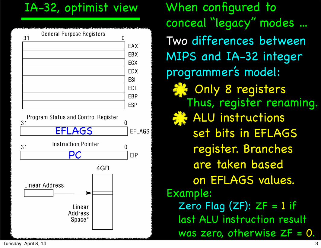
IA-32, optimist view When configured to conceal “legacy” modes ...
EFLAGS
Two differences between MIPS and IA-32 integer programmer’s model:
Only 8 registers
ALU instructions set bits in EFLAGS register. Branches are taken based on EFLAGS values.
Zero Flag (ZF): ZF = 1 if last ALU instruction result was zero, otherwise ZF = 0.
Example:
PC
Thus, register renaming.
3Tuesday, April 8, 14

IA-32, instruction complexity
Even the simple instructions are complex:
ADC m32, r32:
Read the memory location m32, add the contents of register r32 to it, along with the carry bit in EFLAGS, and store the result back in m32.
Rewriting this instruction in MIPS takes at least four instructions: 1 load, 2 adds, 1 store. More for a complex m32 addressing mode.
4Tuesday, April 8, 14

IA-32, addressing modes
3-2 2 Vol. 1
BASIC EXECUTION ENVIRONMENT
The offset which results from adding these components is called an effective address. Each of these components can have either a positive or negative (2s complement) value, with the exception of the scaling factor. Figure 3-11 shows all the possible ways that these components can be combined to create an effective address in the selected segment.
The uses of general-purpose registers as base or index components are restricted in the following manner:
• The ESP register cannot be used as an index register.
• When the ESP or EBP register is used as the base, the SS segment is the default segment. In all other cases, the DS segment is the default segment.
The base, index, and displacement components can be used in any combination, and any of these components can be NULL. A scale factor may be used only when an index also is used. Each possible combination is useful for data structures commonly used by programmers in high-level languages and assembly language.
The following addressing modes suggest uses for common combinations of address components.
• Displacement ⎯ A displacement alone represents a direct (uncomputed) offset to the operand. Because the displacement is encoded in the instruction, this form of an address is sometimes called an absolute or static address. It is commonly used to access a statically allocated scalar operand.
• Base ⎯ A base alone represents an indirect offset to the operand. Since the value in the base register can change, it can be used for dynamic storage of variables and data structures.
• Base + Displacement ⎯ A base register and a displacement can be used together for two distinct purposes:
— As an index into an array when the element size is not 2, 4, or 8 bytes—The displacement component encodes the static offset to the beginning of the array. The base register holds the results of a calculation to determine the offset to a specific element within the array.
— To access a field of a record: the base register holds the address of the beginning of the record, while the displacement is a static offset to the field.
An important special case of this combination is access to parameters in a procedure activation record. A procedure activation record is the stack frame created when a procedure is entered. Here, the EBP register is the best choice for the base register, because it automatically selects the stack segment. This is a compact encoding for this common function.
• (Index ∗ Scale) + Displacement ⎯ This address mode offers an efficient way to index into a static array when the element size is 2, 4, or 8 bytes. The displacement locates the beginning of the array, the index register holds the subscript of the desired array element, and the processor automatically converts the subscript into an index by applying the scaling factor.
• Base + Index + Displacement ⎯ Using two registers together supports either a two-dimensional array (the displacement holds the address of the beginning of the array) or one of several instances of an array of records (the displacement is an offset to a field within the record).
• Base + (Index ∗ Scale) + Displacement ⎯ Using all the addressing components together allows efficient indexing of a two-dimensional array when the elements of the array are 2, 4, or 8 bytes in size.
Figure 3-11. Offset (or Effective Address) Computation
Of fset = Base + (Index * Scale) + Displacement
Base
EAXEBXECXEDXESPEBPESIEDI
EAXEBXECXEDXEBPESIEDI
1 None
2
4
8
8-bit
1 6-bit
3 2-bit
Index Scale Displacement
*+ +
Up to 2 adds and a shift for a memory operand ...
5Tuesday, April 8, 14
IA-32, instruction complexity
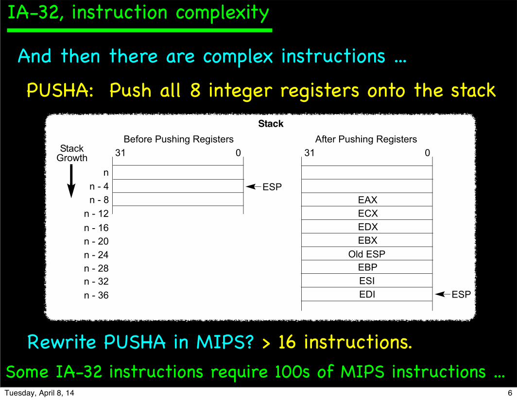
And then there are complex instructions ...PUSHA: Push all 8 integer registers onto the stack
7-6 Vol. 1
PROGRAMMING WITH GENERAL-PURPOSE INSTRUCTIONS
The POP instruction copies the word or doubleword at the current top of stack (indicated by the ESP register) to the location specified with the destination operand. It then increments the ESP register to point to the new top of stack (see Figure 7-3). The destination operand may specify a general-purpose register, a segment register, or a memory location.
The POPA instruction reverses the effect of the PUSHA instruction. It pops the top eight words or doublewords from the top of the stack into the general-purpose registers, except for the ESP register (see Figure 7-4). If the operand-size attribute is 32, the doublewords on the stack are transferred to the registers in the following order: EDI, ESI, EBP, ignore doubleword, EBX, EDX, ECX, and EAX. The ESP register is restored by the action of popping the stack. If the operand-size attribute is 16, the words on the stack are transferred to the registers in the following order: DI, SI, BP, ignore word, BX, DX, CX, and AX.
Figure 7-2. Operation of the PUSHA Instruction
Figure 7-3. Operation of the POP Instruction
0Stack 31Before Pushing Registers
Growth
ESPn - 4n - 8
n
Stack
031After Pushing Registers
ESP
EAX
EDI
EBX
EBP
ECXEDX
Old ESP
ESIn - 36
n - 20
n - 28
n - 12n - 16
n - 24
n - 32
031StackAfter Popping Doubleword
Growth
ESPn - 4n - 8
n
StackBefore Popping Doubleword
ESPDoubleword Value
031
Rewrite PUSHA in MIPS? > 16 instructions.Some IA-32 instructions require 100s of MIPS instructions ...
6Tuesday, April 8, 14

IA-32, instruction decode
IA-32 instructions are 1 to 17 bytes in length.To determine an instruction’s length? Parse it!
Creeping features: Prefix bytes for specifying atomicity, for hinting branch direction, for 8086 mode ...
Vol. 2A 2-1
CHAPTER 2INSTRUCTION FORMAT
This chapter describes the instruction format for all Intel 64 and IA-32 processors. The instruction format for protected mode, real-address mode and virtual-8086 mode is described in Section 2.1. Increments provided for IA-32e mode and its sub-modes are described in Section 2.2.
2.1 INSTRUCTION FORMAT FOR PROTECTED MODE, REAL-ADDRESS MODE, AND VIRTUAL-8086 MODE
The Intel 64 and IA-32 architectures instruction encodings are subsets of the format shown in Figure 2-1. Instruc-tions consist of optional instruction prefixes (in any order), primary opcode bytes (up to three bytes), an addressing-form specifier (if required) consisting of the ModR/M byte and sometimes the SIB (Scale-Index-Base) byte, a displacement (if required), and an immediate data field (if required).
2.1.1 Instruction PrefixesInstruction prefixes are divided into four groups, each with a set of allowable prefix codes. For each instruction, it is only useful to include up to one prefix code from each of the four groups (Groups 1, 2, 3, 4). Groups 1 through 4 may be placed in any order relative to each other.
• Group 1
— Lock and repeat prefixes:
• LOCK prefix is encoded using F0H
• REPNE/REPNZ prefix is encoded using F2H. Repeat-Not-Zero prefix applies only to string and input/output instructions. (F2H is also used as a mandatory prefix for some instructions)
• REP or REPE/REPZ is encoded using F3H. Repeat prefix applies only to string and input/output instruc-tions.(F3H is also used as a mandatory prefix for some instructions)
• Group 2
— Segment override prefixes:
• 2EH—CS segment override (use with any branch instruction is reserved)
• 36H—SS segment override prefix (use with any branch instruction is reserved)
• 3EH—DS segment override prefix (use with any branch instruction is reserved)
• 26H—ES segment override prefix (use with any branch instruction is reserved)
Figure 2-1. Intel 64 and IA-32 Architectures Instruction Format
InstructionPrefixes Opcode ModR/M SIB Displacement Immediat e
Mod R/MReg/Opcode
027 6 5 3
Scale Base
027 6 5 3
Index
Immediatedata of1, 2, or 4bytes or none
Addressdisplacementof 1, 2, or 4bytes or none
1 byte(if required)
1 byte(if required)
1-, 2-, or 3-byteopcode
Up to fourprefixes of1 byte each(optional)
7Tuesday, April 8, 14
UC Regents Spring 2014 © UCBCS 152 L20: Dynamic Scheduling III
Dynamic Execution?
8Tuesday, April 8, 14

UC Regents Fall 2006 © UCBCS 152 L20: Dynamic Scheduling III
Idea: Translate IA-32 opcodes to RISC
Micro-ops:RISC-like instructions that reference the 8 architected registers, plus “temporary” registers.
EFLAGS?Treat each EFLAG bit as an architected register.
Translate?For IA-32 instructions that map into a small number of micro-ops, do translation after decode.
9Tuesday, April 8, 14

UC Regents Fall 2006 © UCBCS 152 L20: Dynamic Scheduling III
Translation example ...ADC m32, r32: // for a simple m32 address mode
Becomes:
LD T1 0(EBX); // EBX register point to m32ADD T1, T1, CF; // CF is carry flag from EFLAGSADD T1, T1, r32; // Add the specified registerST 0(EBX) T1; // Store result back to m32
Instruction traces of IA-32 programs show most executed instructions require 4 or fewer micro-ops.
Translation for these ops are cast into logic gates, often over several pipeline cycles.
10Tuesday, April 8, 14

UC Regents Fall 2006 © UCBCS 152 L20: Dynamic Scheduling III
Complex instructions? Microcode ROM
Instructions like PUSHA are sent to a sequencer that clocks a long sequence of micro-ops out of a ROM.
ROM (combinational)
microPCD Q
ROM entry point of the micro-ops for an IA-32 instruction.
DN
op
+1
01
To register rename
“The micro-op engine”
11Tuesday, April 8, 14
UC Regents Fall 2006 © UCBCS 152 L20: Dynamic Scheduling III
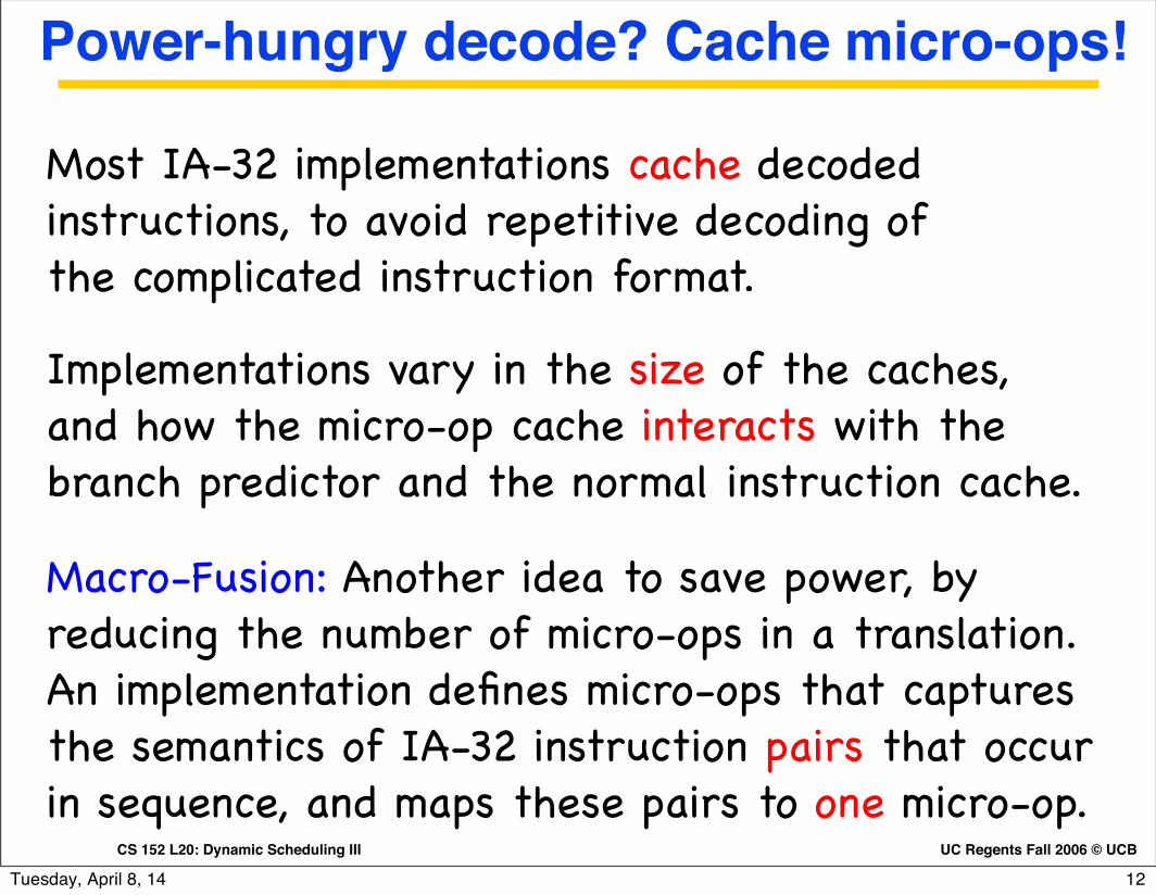
Power-hungry decode? Cache micro-ops!
Most IA-32 implementations cache decoded instructions, to avoid repetitive decoding of the complicated instruction format.
Implementations vary in the size of the caches, and how the micro-op cache interacts with the branch predictor and the normal instruction cache.
Macro-Fusion: Another idea to save power, by reducing the number of micro-ops in a translation. An implementation defines micro-ops that captures the semantics of IA-32 instruction pairs that occur in sequence, and maps these pairs to one micro-op.
12Tuesday, April 8, 14

Execute loop
has 2X clock
1.5 GHz main clock
42M transistors
0.15um process
55 Watts
Intel Pentium
IV(2001)
13Tuesday, April 8, 14

L2 Cache
L1 Data
Cache
Intel Pentium
IV(2001)
Out of Order
Control
Sched.
Green blocks are for OoO
Cyan blocks “fix” IA-32
issues
Decode
Trace Cache
μcode
Integer Pipe
Floating Point PipeGold
blocks are fast
execute pipes
14Tuesday, April 8, 14

HINTON et al.: CMOS IA-32 PROCESSOR WITH 4-GHz INTEGER EXECUTION UNIT 1619
Fig. 3. Pentium® 4 processor microarchitecture organization.
Fig. 4. Processor die photograph.
units and the L1 data cache. On the right of the diagram is thememory subsystem. Fig. 4 is a die photograph showing the phys-ical organization of the processor.
A. Front-EndThe front-end of the Pentium® 4 processor consists of several
units, as shown in the upper part of Fig. 3. It has the instruc-tion translation lookaside buffer (ITLB), the front-end branchpredictor (labeled here Front-End BTB), the IA-32 instructiondecoder, the trace cache, and the microcode ROM.1) Trace Cache: The trace cache is the primary or Level 1
(L1) instruction cache of the Pentium® 4 processor and de-livers up to three micro-operations (UOPs) per clock to theout-of-order execution logic. Most instructions in a programare fetched and executed from the trace cache. Only whenthere is a trace cache miss does the machine fetch and decode
instructions from the Level 2 (L2) cache. This occurs about asoften as previous processors miss their L1 instruction cache.The trace cache has a capacity to hold up to 12K UOPs. It hasa similar hit rate to an 8K–16K-byte conventional instructioncache.IA-32 instructions are cumbersome to decode. The instruc-
tions have a variable number of bytes and have many differentoptions. The instruction decoding logic needs to sort this all outand convert these complex instructions into simple UOPs thatthe machine knows how to execute. This decoding is especiallydifficult when trying to decode several IA-32 instructions eachclock cycle when running at the high clock frequency of the Pen-tium® 4 processor. A high-bandwidth IA-32 decoder, capableof decoding several instructions per clock cycle, takes severalpipeline stages to do its work. When a branch is mispredicted,the recovery time is much shorter if the machine does not haveto redecode the IA-32 instructions needed to resume executionat the corrected branch target location. By caching the UOPs ofthe previously decoded instructions in the trace cache, instruc-tions bypass the instruction decoder most of the time, therebyreducing misprediction latency and allowing a simpler decoderthat processes only one IA-32 instruction per clock cycle.The trace cache takes the already decoded UOPs from the
IA-32 Instruction Decoder and assembles or builds them intoprogram-ordered sequences of UOPs called traces. It packs theUOPs into groups of six UOPs per trace line. There can be manytrace lines in a single trace. These traces consist of UOPs run-ning sequentially down the predicted path of the IA-32 programexecution. This allows the target of a branch to be included inthe same trace cache line as the branch itself even if the branchand its target instructions are thousands of bytes apart in the pro-gram.Conventional instruction caches typically provide instruc-
tions up to and including a taken branch instruction, but
Intel Pentium IV
(2001)
Cyan blocks “fix” IA-32
issues
Green blocks are for OoO
Gold blocks are fast execute
pipes
15Tuesday, April 8, 14

HINTON et al.: CMOS IA-32 PROCESSOR WITH 4-GHz INTEGER EXECUTION UNIT 1619
Fig. 3. Pentium® 4 processor microarchitecture organization.
Fig. 4. Processor die photograph.
units and the L1 data cache. On the right of the diagram is thememory subsystem. Fig. 4 is a die photograph showing the phys-ical organization of the processor.
A. Front-EndThe front-end of the Pentium® 4 processor consists of several
units, as shown in the upper part of Fig. 3. It has the instruc-tion translation lookaside buffer (ITLB), the front-end branchpredictor (labeled here Front-End BTB), the IA-32 instructiondecoder, the trace cache, and the microcode ROM.1) Trace Cache: The trace cache is the primary or Level 1
(L1) instruction cache of the Pentium® 4 processor and de-livers up to three micro-operations (UOPs) per clock to theout-of-order execution logic. Most instructions in a programare fetched and executed from the trace cache. Only whenthere is a trace cache miss does the machine fetch and decode
instructions from the Level 2 (L2) cache. This occurs about asoften as previous processors miss their L1 instruction cache.The trace cache has a capacity to hold up to 12K UOPs. It hasa similar hit rate to an 8K–16K-byte conventional instructioncache.IA-32 instructions are cumbersome to decode. The instruc-
tions have a variable number of bytes and have many differentoptions. The instruction decoding logic needs to sort this all outand convert these complex instructions into simple UOPs thatthe machine knows how to execute. This decoding is especiallydifficult when trying to decode several IA-32 instructions eachclock cycle when running at the high clock frequency of the Pen-tium® 4 processor. A high-bandwidth IA-32 decoder, capableof decoding several instructions per clock cycle, takes severalpipeline stages to do its work. When a branch is mispredicted,the recovery time is much shorter if the machine does not haveto redecode the IA-32 instructions needed to resume executionat the corrected branch target location. By caching the UOPs ofthe previously decoded instructions in the trace cache, instruc-tions bypass the instruction decoder most of the time, therebyreducing misprediction latency and allowing a simpler decoderthat processes only one IA-32 instruction per clock cycle.The trace cache takes the already decoded UOPs from the
IA-32 Instruction Decoder and assembles or builds them intoprogram-ordered sequences of UOPs called traces. It packs theUOPs into groups of six UOPs per trace line. There can be manytrace lines in a single trace. These traces consist of UOPs run-ning sequentially down the predicted path of the IA-32 programexecution. This allows the target of a branch to be included inthe same trace cache line as the branch itself even if the branchand its target instructions are thousands of bytes apart in the pro-gram.Conventional instruction caches typically provide instruc-
tions up to and including a taken branch instruction, but
Branch predictor steers instruction prefetch from L2. Maximum decoder rate is 1 IA-32 instruction per cycle.
Trace cache: 12K micro-ops: 2K lines hold 6 decoded micro-ops in executed (trace) order, that follow taken branches and function calls.Prediction: Each line includes a prediction of next trace line to fetch. The front-end prefetcher takes over on a trace cache miss.Microcode ROM: Trace cache jumps into ROM if IA-32 instruction maps to > 4 micro-ops.
16Tuesday, April 8, 14

HINTON et al.: CMOS IA-32 PROCESSOR WITH 4-GHz INTEGER EXECUTION UNIT 1619
Fig. 3. Pentium® 4 processor microarchitecture organization.
Fig. 4. Processor die photograph.
units and the L1 data cache. On the right of the diagram is thememory subsystem. Fig. 4 is a die photograph showing the phys-ical organization of the processor.
A. Front-EndThe front-end of the Pentium® 4 processor consists of several
units, as shown in the upper part of Fig. 3. It has the instruc-tion translation lookaside buffer (ITLB), the front-end branchpredictor (labeled here Front-End BTB), the IA-32 instructiondecoder, the trace cache, and the microcode ROM.1) Trace Cache: The trace cache is the primary or Level 1
(L1) instruction cache of the Pentium® 4 processor and de-livers up to three micro-operations (UOPs) per clock to theout-of-order execution logic. Most instructions in a programare fetched and executed from the trace cache. Only whenthere is a trace cache miss does the machine fetch and decode
instructions from the Level 2 (L2) cache. This occurs about asoften as previous processors miss their L1 instruction cache.The trace cache has a capacity to hold up to 12K UOPs. It hasa similar hit rate to an 8K–16K-byte conventional instructioncache.IA-32 instructions are cumbersome to decode. The instruc-
tions have a variable number of bytes and have many differentoptions. The instruction decoding logic needs to sort this all outand convert these complex instructions into simple UOPs thatthe machine knows how to execute. This decoding is especiallydifficult when trying to decode several IA-32 instructions eachclock cycle when running at the high clock frequency of the Pen-tium® 4 processor. A high-bandwidth IA-32 decoder, capableof decoding several instructions per clock cycle, takes severalpipeline stages to do its work. When a branch is mispredicted,the recovery time is much shorter if the machine does not haveto redecode the IA-32 instructions needed to resume executionat the corrected branch target location. By caching the UOPs ofthe previously decoded instructions in the trace cache, instruc-tions bypass the instruction decoder most of the time, therebyreducing misprediction latency and allowing a simpler decoderthat processes only one IA-32 instruction per clock cycle.The trace cache takes the already decoded UOPs from the
IA-32 Instruction Decoder and assembles or builds them intoprogram-ordered sequences of UOPs called traces. It packs theUOPs into groups of six UOPs per trace line. There can be manytrace lines in a single trace. These traces consist of UOPs run-ning sequentially down the predicted path of the IA-32 programexecution. This allows the target of a branch to be included inthe same trace cache line as the branch itself even if the branchand its target instructions are thousands of bytes apart in the pro-gram.Conventional instruction caches typically provide instruc-
tions up to and including a taken branch instruction, but
Outoforder logic1622 IEEE JOURNAL OF SOLID-STATE CIRCUITS, VOL. 36, NO. 11, NOVEMBER 2001
Fig. 6. Important logic loops.
Fig. 7. Staggered ALU design in 16-b slices.
This high-speed ALU core is kept as small as possible to min-imize the metal length and loading. Only the essential hardwarenecessary to perform the frequent ALU operations is includedin this high-speed ALU execution loop. Functions that are notused very frequently in most integer programs are not put in thislow-latency ALU loop, but are put elsewhere. Some examplesof integer execution hardware put elsewhere are the multiplier,shifts, flag logic, and branch processing.Determining if the data obtained was correct, or if it was a
cache miss, TLB miss, or protection violation, or if it had someform of interaction with other things in the memory system, ismore complex and takes longer than getting the data. Hence,the first-level data cache data path is in the high-speed core, butthe more extensive logic for determining if the data obtained iscorrect is placed elsewhere.The processor does ALU operations with an effective latency
of one-half of a clock cycle. It does this operation in a sequenceof three fast clock cycles (the fast clock runs at 2 the mainclock rate), as shown in Fig. 7. In the first fast clock cycle, thelow-order 16 bits are computed and are immediately available tofeed the low 16 bits of a dependent operation the very next fastclock cycle. The high-order 16 bits are processed in the next fastcycle, using the carryout just generated by the low 16-b opera-
Fig. 8. ALU inputs, loading, and bypass loop.
tion. This upper 16-b result will be available to the next depen-dent operation exactly when needed. This is called a staggeredadd. The ALU flags are processed in the third fast cycle. Thisstaggered add means that only a 16-b adder and its input muxesneed to be completed in a fast clock cycle. The low-order 16bits are needed at one time in order to begin the access of the L1data cache when used as an address input.To maximize operating frequency, the first-level bypass mul-
tiplexers are restricted to four inputs (Fig. 8). These four inputsinclude the two ALU outputs, the output of the first level datacache, and the output of a multistage bypass network that wasresolved during the previous clock. Similarly, the output loadingof the execution units is strictly controlled. The execution unitsdrive seven output loads: the six first-level bypass multiplexers(two per adder) and a latch that buffers all other uses of the ex-ecution unit output.The ALU includes selectable inversion of each source of
one operand and selectable carry blocking at byte boundaries,as well as sign extension and a full set of logic functions. TheALU adder is a propagate–generate–kill addition algorithm(PGK) true-and-complement design. A jam latch at the finaldomino stage provides the required hold time to close theloop and redrive the inputs of the ALUs themselves and theaddress generator for the load. The add loop, including theinput multiplexer with built-in selectable inverter, the selectable
3 micro-ops per cycle
from trace cache
6 operations scheduled per cycle
3 micro-ops retired
per cycle
126 instructions in flight
128 integer physical registers128 floating point physical registers
17Tuesday, April 8, 14

HINTON et al.: CMOS IA-32 PROCESSOR WITH 4-GHz INTEGER EXECUTION UNIT 1619
Fig. 3. Pentium® 4 processor microarchitecture organization.
Fig. 4. Processor die photograph.
units and the L1 data cache. On the right of the diagram is thememory subsystem. Fig. 4 is a die photograph showing the phys-ical organization of the processor.
A. Front-EndThe front-end of the Pentium® 4 processor consists of several
units, as shown in the upper part of Fig. 3. It has the instruc-tion translation lookaside buffer (ITLB), the front-end branchpredictor (labeled here Front-End BTB), the IA-32 instructiondecoder, the trace cache, and the microcode ROM.1) Trace Cache: The trace cache is the primary or Level 1
(L1) instruction cache of the Pentium® 4 processor and de-livers up to three micro-operations (UOPs) per clock to theout-of-order execution logic. Most instructions in a programare fetched and executed from the trace cache. Only whenthere is a trace cache miss does the machine fetch and decode
instructions from the Level 2 (L2) cache. This occurs about asoften as previous processors miss their L1 instruction cache.The trace cache has a capacity to hold up to 12K UOPs. It hasa similar hit rate to an 8K–16K-byte conventional instructioncache.IA-32 instructions are cumbersome to decode. The instruc-
tions have a variable number of bytes and have many differentoptions. The instruction decoding logic needs to sort this all outand convert these complex instructions into simple UOPs thatthe machine knows how to execute. This decoding is especiallydifficult when trying to decode several IA-32 instructions eachclock cycle when running at the high clock frequency of the Pen-tium® 4 processor. A high-bandwidth IA-32 decoder, capableof decoding several instructions per clock cycle, takes severalpipeline stages to do its work. When a branch is mispredicted,the recovery time is much shorter if the machine does not haveto redecode the IA-32 instructions needed to resume executionat the corrected branch target location. By caching the UOPs ofthe previously decoded instructions in the trace cache, instruc-tions bypass the instruction decoder most of the time, therebyreducing misprediction latency and allowing a simpler decoderthat processes only one IA-32 instruction per clock cycle.The trace cache takes the already decoded UOPs from the
IA-32 Instruction Decoder and assembles or builds them intoprogram-ordered sequences of UOPs called traces. It packs theUOPs into groups of six UOPs per trace line. There can be manytrace lines in a single trace. These traces consist of UOPs run-ning sequentially down the predicted path of the IA-32 programexecution. This allows the target of a branch to be included inthe same trace cache line as the branch itself even if the branchand its target instructions are thousands of bytes apart in the pro-gram.Conventional instruction caches typically provide instruc-
tions up to and including a taken branch instruction, but
Execution Unit:Simple integer ALUsruns on both edges of the 1.5 Ghz clock.
Data cache speculates
on L1 hit, and has a 2 cycle
load-use delay.48 load + 24 store buffers also within
this critical loop.
1622 IEEE JOURNAL OF SOLID-STATE CIRCUITS, VOL. 36, NO. 11, NOVEMBER 2001
Fig. 6. Important logic loops.
Fig. 7. Staggered ALU design in 16-b slices.
This high-speed ALU core is kept as small as possible to min-imize the metal length and loading. Only the essential hardwarenecessary to perform the frequent ALU operations is includedin this high-speed ALU execution loop. Functions that are notused very frequently in most integer programs are not put in thislow-latency ALU loop, but are put elsewhere. Some examplesof integer execution hardware put elsewhere are the multiplier,shifts, flag logic, and branch processing.Determining if the data obtained was correct, or if it was a
cache miss, TLB miss, or protection violation, or if it had someform of interaction with other things in the memory system, ismore complex and takes longer than getting the data. Hence,the first-level data cache data path is in the high-speed core, butthe more extensive logic for determining if the data obtained iscorrect is placed elsewhere.The processor does ALU operations with an effective latency
of one-half of a clock cycle. It does this operation in a sequenceof three fast clock cycles (the fast clock runs at 2 the mainclock rate), as shown in Fig. 7. In the first fast clock cycle, thelow-order 16 bits are computed and are immediately available tofeed the low 16 bits of a dependent operation the very next fastclock cycle. The high-order 16 bits are processed in the next fastcycle, using the carryout just generated by the low 16-b opera-
Fig. 8. ALU inputs, loading, and bypass loop.
tion. This upper 16-b result will be available to the next depen-dent operation exactly when needed. This is called a staggeredadd. The ALU flags are processed in the third fast cycle. Thisstaggered add means that only a 16-b adder and its input muxesneed to be completed in a fast clock cycle. The low-order 16bits are needed at one time in order to begin the access of the L1data cache when used as an address input.To maximize operating frequency, the first-level bypass mul-
tiplexers are restricted to four inputs (Fig. 8). These four inputsinclude the two ALU outputs, the output of the first level datacache, and the output of a multistage bypass network that wasresolved during the previous clock. Similarly, the output loadingof the execution units is strictly controlled. The execution unitsdrive seven output loads: the six first-level bypass multiplexers(two per adder) and a latch that buffers all other uses of the ex-ecution unit output.The ALU includes selectable inversion of each source of
one operand and selectable carry blocking at byte boundaries,as well as sign extension and a full set of logic functions. TheALU adder is a propagate–generate–kill addition algorithm(PGK) true-and-complement design. A jam latch at the finaldomino stage provides the required hold time to close theloop and redrive the inputs of the ALUs themselves and theaddress generator for the load. The add loop, including theinput multiplexer with built-in selectable inverter, the selectable
2X
2X
2XBypass Network:Fast ALUscan usetheir own results on each edge.
18Tuesday, April 8, 14

1622 IEEE JOURNAL OF SOLID-STATE CIRCUITS, VOL. 36, NO. 11, NOVEMBER 2001
Fig. 6. Important logic loops.
Fig. 7. Staggered ALU design in 16-b slices.
This high-speed ALU core is kept as small as possible to min-imize the metal length and loading. Only the essential hardwarenecessary to perform the frequent ALU operations is includedin this high-speed ALU execution loop. Functions that are notused very frequently in most integer programs are not put in thislow-latency ALU loop, but are put elsewhere. Some examplesof integer execution hardware put elsewhere are the multiplier,shifts, flag logic, and branch processing.Determining if the data obtained was correct, or if it was a
cache miss, TLB miss, or protection violation, or if it had someform of interaction with other things in the memory system, ismore complex and takes longer than getting the data. Hence,the first-level data cache data path is in the high-speed core, butthe more extensive logic for determining if the data obtained iscorrect is placed elsewhere.The processor does ALU operations with an effective latency
of one-half of a clock cycle. It does this operation in a sequenceof three fast clock cycles (the fast clock runs at 2 the mainclock rate), as shown in Fig. 7. In the first fast clock cycle, thelow-order 16 bits are computed and are immediately available tofeed the low 16 bits of a dependent operation the very next fastclock cycle. The high-order 16 bits are processed in the next fastcycle, using the carryout just generated by the low 16-b opera-
Fig. 8. ALU inputs, loading, and bypass loop.
tion. This upper 16-b result will be available to the next depen-dent operation exactly when needed. This is called a staggeredadd. The ALU flags are processed in the third fast cycle. Thisstaggered add means that only a 16-b adder and its input muxesneed to be completed in a fast clock cycle. The low-order 16bits are needed at one time in order to begin the access of the L1data cache when used as an address input.To maximize operating frequency, the first-level bypass mul-
tiplexers are restricted to four inputs (Fig. 8). These four inputsinclude the two ALU outputs, the output of the first level datacache, and the output of a multistage bypass network that wasresolved during the previous clock. Similarly, the output loadingof the execution units is strictly controlled. The execution unitsdrive seven output loads: the six first-level bypass multiplexers(two per adder) and a latch that buffers all other uses of the ex-ecution unit output.The ALU includes selectable inversion of each source of
one operand and selectable carry blocking at byte boundaries,as well as sign extension and a full set of logic functions. TheALU adder is a propagate–generate–kill addition algorithm(PGK) true-and-complement design. A jam latch at the finaldomino stage provides the required hold time to close theloop and redrive the inputs of the ALUs themselves and theaddress generator for the load. The add loop, including theinput multiplexer with built-in selectable inverter, the selectable
Key trick: Staggered ALUs
Pipelineregistersadded tocarry chain.A 32-bitadder iscomputingparts of 3 different operations at the same time.
HINTON et al.: CMOS IA-32 PROCESSOR WITH 4-GHz INTEGER EXECUTION UNIT 1623
Fig. 9. ALU design in global STP: a typical bit.
Fig. 10. Laser voltage probe of 4-GHz ALU operation.
carry blocker, and the PGK logic, requires eight logic inversionlevels (Fig. 9).The fundamental logic family used in the ALUs is a type
of self-resetting domino [6] internally called Globally ResetDomino with Self-Terminating Precharge (Global STP). The2-GHz clock that is globally distributed is doubled locally togenerate a 4-GHz clock with a self-timed phase boundary. Eachgate cycles at 4 GHz, i.e., evaluation, precharge, and termina-tion of the precharge signal are all completed within 250 ps,including all appropriate timing margins, and the gate is readyto receive new data. The state is held in the second-to-last stage.In the beginning of a 4-GHz cycle, the last two stages are beingreset while the first six logic stages of the ALUs (three dominoand three static) go through an evaluation. After the precharge ofthe second-to-last stage has been turned off, the evaluate signalpropagates to the output, where it is held until the next cycle. Thefirst six stages, however, are reset in the same cycle in whichthey have evaluated. The precharge of these stages is globallyinitiated by a suitably delayed clock and is locally terminated,allowing a faster cycle time than if the precharge signal was ter-minated by the global reset clock. A representative bit with theglobal reset circuitry is shown in Fig. 9.Fig. 10 shows laser voltage probe [7] results for two clocks
and two internal ALU signals. The clocks shown are the 2-GHzmain clock and the generated 4-GHz local clock. The two sig-nals show a one-clock output pulse and a multiclock latched re-sult.
2) Complex Integer Operations: The simple, very frequentALU operations go to the high-speed integer ALU executionunits described above. Integer operations that are more complexgo to separate hardware for completion. Most integer shift orrotate operations go to the complex integer dispatch port. Theseshift operations have a latency of four clocks. Integer multiplyand divide operations also have a long latency. Typical forms ofmultiply and divide have a latency of about 14 and 60 clocks,respectively.3) Low-Latency L1 Data Cache: The L1 data cache
is an 8K-byte cache that is used for both integer andfloating-point/SSE loads and stores. It is organized as afour-way set-associative cache that has 64 B per cache line. It isa write-through cache, which means that writes to it are alwayscopied into the L2 cache. It can do one load and one store perclock cycle, each of which can be up to 16 B long.The latency of load operations is a key aspect of processor
performance. This is especially true for IA-32 programs thathave many loads and stores because of the limited number ofregisters in the instruction set. The Pentium® 4 microarchitec-ture optimizes for the lowest overall load-access latency witha small very low-latency 8K-byte cache backed up by a largehigh-bandwidth second-level cache with medium latency. Formost IA-32 programs, this configuration of a small but verylow-latency L1 data cache followed by a large medium-latencyL2 cache gives lower net load-access latency and, therefore,higher performance than a larger, slower L1 cache. The L1 datacache operates with a two-clock load-use latency for integerloads and a six-clock load-use latency for floating-point/SSEloads.This two-clock load latency is difficult to achieve with the
high clock rates of the Pentium® 4 processor. The cache accessalgorithms leverage the fact that almost all accesses hit the first-level data cache and the data TLB (DTLB) to enable the two-cycle load-access latency.At this high frequency and with this deep machine pipeline,
the distance in clocks, from the load scheduler to execution, islonger than the load execution latency itself. The UOP sched-ulers dispatch dependent operations before the parent load hasfinished executing. In most cases, the scheduler assumes thatthe load will hit the L1 data cache. If the load misses the L1
19Tuesday, April 8, 14

1622 IEEE JOURNAL OF SOLID-STATE CIRCUITS, VOL. 36, NO. 11, NOVEMBER 2001
Fig. 6. Important logic loops.
Fig. 7. Staggered ALU design in 16-b slices.
This high-speed ALU core is kept as small as possible to min-imize the metal length and loading. Only the essential hardwarenecessary to perform the frequent ALU operations is includedin this high-speed ALU execution loop. Functions that are notused very frequently in most integer programs are not put in thislow-latency ALU loop, but are put elsewhere. Some examplesof integer execution hardware put elsewhere are the multiplier,shifts, flag logic, and branch processing.Determining if the data obtained was correct, or if it was a
cache miss, TLB miss, or protection violation, or if it had someform of interaction with other things in the memory system, ismore complex and takes longer than getting the data. Hence,the first-level data cache data path is in the high-speed core, butthe more extensive logic for determining if the data obtained iscorrect is placed elsewhere.The processor does ALU operations with an effective latency
of one-half of a clock cycle. It does this operation in a sequenceof three fast clock cycles (the fast clock runs at 2 the mainclock rate), as shown in Fig. 7. In the first fast clock cycle, thelow-order 16 bits are computed and are immediately available tofeed the low 16 bits of a dependent operation the very next fastclock cycle. The high-order 16 bits are processed in the next fastcycle, using the carryout just generated by the low 16-b opera-
Fig. 8. ALU inputs, loading, and bypass loop.
tion. This upper 16-b result will be available to the next depen-dent operation exactly when needed. This is called a staggeredadd. The ALU flags are processed in the third fast cycle. Thisstaggered add means that only a 16-b adder and its input muxesneed to be completed in a fast clock cycle. The low-order 16bits are needed at one time in order to begin the access of the L1data cache when used as an address input.To maximize operating frequency, the first-level bypass mul-
tiplexers are restricted to four inputs (Fig. 8). These four inputsinclude the two ALU outputs, the output of the first level datacache, and the output of a multistage bypass network that wasresolved during the previous clock. Similarly, the output loadingof the execution units is strictly controlled. The execution unitsdrive seven output loads: the six first-level bypass multiplexers(two per adder) and a latch that buffers all other uses of the ex-ecution unit output.The ALU includes selectable inversion of each source of
one operand and selectable carry blocking at byte boundaries,as well as sign extension and a full set of logic functions. TheALU adder is a propagate–generate–kill addition algorithm(PGK) true-and-complement design. A jam latch at the finaldomino stage provides the required hold time to close theloop and redrive the inputs of the ALUs themselves and theaddress generator for the load. The add loop, including theinput multiplexer with built-in selectable inverter, the selectable
In context: complete datapath
The logic loops used 90% of the time run at 3 GHz, but most of the chip runs at 1500 MHz.
20Tuesday, April 8, 14

1618 IEEE JOURNAL OF SOLID-STATE CIRCUITS, VOL. 36, NO. 11, NOVEMBER 2001
Fig. 1. Relative frequencies of Intel processors if fabricated on same process.
Fig. 2. Branch misprediction pipeline.
able to achieve about a 1.5 times higher frequency on the sameprocess technology.The Pentium® 4 microarchitecture was designed to have an
even deeper pipeline (about two times the Pentium® III microar-chitecture) with even fewer gates of logic per clock cycle toallow an industry-leading microprocessor clock rate in 0.18- mCMOS. Compared to the Pentium® III family of processors,the Pentium® 4 processor was designed with a greater than 1.6times higher frequency target for its main clock rate, on thesame process technology. This allows it to operate at a muchhigher frequency than the Pentium® III family of processorson the same silicon process technology. At its introduction inNovember 2000, the Pentium® 4 processor was at 1.5 times thefrequency of the Pentium® III processor. Over time, this fre-quency delta will increase as the Pentium® 4 processor manu-facturing matures, and critical paths are eliminated by designrevisions.Different parts of the Pentium® 4 processor run at different
clock frequencies. The frequency of each section of logic is setto be appropriate for the performance it needs to achieve. Thehighest frequency section (fast clock) was set equal to the speedof the critical ALU-bypass execution loop that is used for mostinstructions in integer programs.Most other parts of the chip runat half of the 4-GHz fast clock, since thismakes these partsmuch
easier to design. A few sections of the chip run at a quarter ofthis fast-clock frequency,making them also easier to design. The2-GHz clock is distributed across the die, and the other neededfrequencies are generated locally [2]. The bus logic runs at 100MHz, to match the system bus needs.As an example of the pipelining differences, Fig. 2 shows a
key pipeline in both the Pentium® III and the Pentium® 4 pro-cessors: the mispredicted branch pipeline.This pipeline covers the cycles it takes a processor to recover
from a branch that went a different direction than the early fetchhardware predicted at the beginning of the machine pipeline.As shown, the Pentium® 4 processor has a 20-stage mispre-diction pipeline, while the Pentium® III microarchitecture hasa 10-stage misprediction pipeline. By dividing the pipelineinto smaller pieces, doing less work during each pipeline stage(fewer gates of logic), the clock rate can be much higher.
III. PENTIUM® 4 MICROARCHITECTURE
Fig. 3 shows a detailed block diagram of the organization ofthe Pentium® 4 processor. The top-left portion of the diagramshows the front-end part of the machine. The middle of the dia-gram illustrates the out-of-order buffering logic, and the bottomof the diagram shows the integer and floating-point execution
In actuality: The clock went too fast
The trace cache was too much of a departure from Pentium III, and the existing code base missed the cache too often. This was particularly bad because the Pentium IV pipeline had so many stages!
21Tuesday, April 8, 14

UC Regents Fall 2013 © UCBCS 250 L3: Timing
Recall: Limits to super-pipelining ...
Francois Labonte
[email protected] 4/23/2003 Stanford University
Cycle in FO4
0
10
20
30
40
50
60
70
80
90
100
85 86 87 88 89 90 91 92 93 94 95 96 97 98 99 00 01 02 03 04 05
intel 386
intel 486
intel pentium
intel pentium 2
intel pentium 3
intel pentium 4
intel itanium
Alpha 21064
Alpha 21164
Alpha 21264
Sparc
SuperSparc
Sparc64
Mips
HP PA
Power PC
AMD K6
AMD K7
AMD x86-64
Thanks to Francois Labonte, Stanford
FO4Delays
Historicallimit:about
12 FO4s
CPU Clock Periods1985-2005
MIPS 20005 stages
Pentium 420 stages
Pentium Pro10 stages
*
Power wall:Intel Core Duo has 14 stages
FO4: How many fanout-of-4 inverter delays in the clock period.
22Tuesday, April 8, 14

The Pentium IV was the chip that foreshadowed the “power wall”.
Upper-management pressure for a high clock rate (for marketing) pushed the design team to use too many pipeline stages, and performance (and power) suffered.
Intel recovered by going back to their earlier Pentium Pro out-of-order design ...
Many elements of the Pentium IV are innovative ... and were reintroduced in Sandy Bridge (2011-onward).
23Tuesday, April 8, 14

It’s all in the timing ...
The dot-com tech stock “bubble”
Pentium IV chiprelease date
24Tuesday, April 8, 14

UC Regents Spring 2014 © UCBCS 152 L20: Dynamic Scheduling III
Break
Play:25Tuesday, April 8, 14

Sandy Bridge
LLC and ring stopOut-of-order core
26Tuesday, April 8, 14

4 Sandy Bridge Spans Generations
SEPTEMBER 2010
ance improvement is thus minimal. More importantly, instructions whose micro-ops are already in the L0 cache do not need to be fetched, predecoded, decoded, and con-verted to micro-ops. Thus, the new cache reduces the power used for these complex tasks by about 80%.
Aside from the AVX changes, Sandy Bridge uses the same execution core as Nehalem. Its 32KB data cache is backed by a 256KB level-two (L2) cache, as Figure 3 shows. Nehalem’s data cache, however, supports one 128-bit load and one 128-bit store per cycle. Sandy Bridge can perform two loads and one store per cycle, doubling the load band-width. This change helps support the AVX instructions, enabling the cache to perform one 256-bit AVX load per cycle. AVX stores require two cycles to complete.
Ring Around the Cores Sandy Bridge contains a new component, the system agent, that controls what was previously called the north bridge: the memory controller, PCI Express, display interfaces, and the DMI connection to the external south-bridge chip (PCH). The exact system interfaces will vary depending on the target platform, but the initial products will support two DDR3 SDRAM channels and a single ×16 PCI Express 2.0 interface that can also be configured as two ×8 ports. The chip uses the Embedded DisplayPort interface to con-nect to the internal display in a notebook computer. Other display and system interfaces are in the south bridge.
Instead of the single L3 cache used in Nehalem and Westmere, Sandy Bridge divides the L3 cache into four
blocks. Intel has not disclosed details, but we expect each block to be 2MB in size, totaling 8MB of L3 cache in a four-CPU processor. Although each CPU is physically adjacent to one of the cache blocks, there is no association of data between the CPU and its neighboring cache block. Instead, each CPU simply sees a single, large L3 cache. Di-viding this cache into four blocks, however, allows each block to service requests simultaneously, quadrupling the total cache bandwidth. At 3.4GHz, the L3 cache can deliver 435GB/s.
To improve bus bandwidth and simplify scalability, Sandy Bridge implements a ring interconnect instead of the usual internal bus. Intel used a ring in Nehalem-EX and in its ill-fated Larrabee (see MPR 9/29/08-01, “Intel’s Larrabee Redefines GPUs”), but it has not previously used this structure in its mainstream processors. Other proces-sors use rings—notably, NetLogic’s XLR and XLP (see MPR 7/26/10-01, “NetLogic Broadens XLP Family”).
Because each station in the ring connects only to the next station, the ring segments are short enough to operate at the full CPU speed. Furthermore, each ring segment can potentially carry different data. (The Sandy Bridge design actually includes four separate rings: one for data and three for address, coherency, and control information.) The downside of a ring is that data may need to traverse mul-tiple hops to get to its destination. These extra hops add latency, but given the faster speed of the ring, two or even three hops can take as little time as a single transfer on a traditional multidrop bus.
Sandy Bridge implements a unique type of ring that minimizes the number of hops. As Figure 4 shows, the ring has 10 stations, but each CPU/cache block shares two stations, one connected to the portion of the ring going “up” and the other connected to the portion going “down.” For each transfer, the ring interface chooses the direction, up or down, that will get the data to its des-tination the soonest. In this configu-ration, the worst-case number of hops to or from any CPU or cache is four. Be-cause a CPU can access its associated cache block without using the ring (i.e., zero hops), the average trip from a CPU to cache is only 1.25 hops. The average trip from a CPU/cache to or from the GPU or the system agent is 2.5 hops. As a result, the average L3 cache latency is 26 to 31 cycles compared with about 36 in Nehalem.
Assuming that 25% of the cache traffic passes directly through to its neighboring CPU without getting on the ring, the ring itself must handle three
Figure 3. Complete block diagram of Sandy Bridge CPU. Important changes from Nehalem include an improved branch predictor, a new micro-op cache, new AVX registers and execution units, and the ability to load two 128-bit values per cycle from the data cache.
Sandy Bridge
27Tuesday, April 8, 14

4 Sandy Bridge Spans Generations
SEPTEMBER 2010
ance improvement is thus minimal. More importantly, instructions whose micro-ops are already in the L0 cache do not need to be fetched, predecoded, decoded, and con-verted to micro-ops. Thus, the new cache reduces the power used for these complex tasks by about 80%.
Aside from the AVX changes, Sandy Bridge uses the same execution core as Nehalem. Its 32KB data cache is backed by a 256KB level-two (L2) cache, as Figure 3 shows. Nehalem’s data cache, however, supports one 128-bit load and one 128-bit store per cycle. Sandy Bridge can perform two loads and one store per cycle, doubling the load band-width. This change helps support the AVX instructions, enabling the cache to perform one 256-bit AVX load per cycle. AVX stores require two cycles to complete.
Ring Around the Cores Sandy Bridge contains a new component, the system agent, that controls what was previously called the north bridge: the memory controller, PCI Express, display interfaces, and the DMI connection to the external south-bridge chip (PCH). The exact system interfaces will vary depending on the target platform, but the initial products will support two DDR3 SDRAM channels and a single ×16 PCI Express 2.0 interface that can also be configured as two ×8 ports. The chip uses the Embedded DisplayPort interface to con-nect to the internal display in a notebook computer. Other display and system interfaces are in the south bridge.
Instead of the single L3 cache used in Nehalem and Westmere, Sandy Bridge divides the L3 cache into four
blocks. Intel has not disclosed details, but we expect each block to be 2MB in size, totaling 8MB of L3 cache in a four-CPU processor. Although each CPU is physically adjacent to one of the cache blocks, there is no association of data between the CPU and its neighboring cache block. Instead, each CPU simply sees a single, large L3 cache. Di-viding this cache into four blocks, however, allows each block to service requests simultaneously, quadrupling the total cache bandwidth. At 3.4GHz, the L3 cache can deliver 435GB/s.
To improve bus bandwidth and simplify scalability, Sandy Bridge implements a ring interconnect instead of the usual internal bus. Intel used a ring in Nehalem-EX and in its ill-fated Larrabee (see MPR 9/29/08-01, “Intel’s Larrabee Redefines GPUs”), but it has not previously used this structure in its mainstream processors. Other proces-sors use rings—notably, NetLogic’s XLR and XLP (see MPR 7/26/10-01, “NetLogic Broadens XLP Family”).
Because each station in the ring connects only to the next station, the ring segments are short enough to operate at the full CPU speed. Furthermore, each ring segment can potentially carry different data. (The Sandy Bridge design actually includes four separate rings: one for data and three for address, coherency, and control information.) The downside of a ring is that data may need to traverse mul-tiple hops to get to its destination. These extra hops add latency, but given the faster speed of the ring, two or even three hops can take as little time as a single transfer on a traditional multidrop bus.
Sandy Bridge implements a unique type of ring that minimizes the number of hops. As Figure 4 shows, the ring has 10 stations, but each CPU/cache block shares two stations, one connected to the portion of the ring going “up” and the other connected to the portion going “down.” For each transfer, the ring interface chooses the direction, up or down, that will get the data to its des-tination the soonest. In this configu-ration, the worst-case number of hops to or from any CPU or cache is four. Be-cause a CPU can access its associated cache block without using the ring (i.e., zero hops), the average trip from a CPU to cache is only 1.25 hops. The average trip from a CPU/cache to or from the GPU or the system agent is 2.5 hops. As a result, the average L3 cache latency is 26 to 31 cycles compared with about 36 in Nehalem.
Assuming that 25% of the cache traffic passes directly through to its neighboring CPU without getting on the ring, the ring itself must handle three
Figure 3. Complete block diagram of Sandy Bridge CPU. Important changes from Nehalem include an improved branch predictor, a new micro-op cache, new AVX registers and execution units, and the ability to load two 128-bit values per cycle from the data cache.
Front End
Traditional L1 instruction cache does the “heavy lifting”. Caches IA-32 instructions.
Decoders can generate 4 micro-ops/cycle.Microcode ROM still a part of decode.
Micro-op cache is 10% of the size of the Pentium IV trace cache. Purpose is power savings (80% of time, decode off).
28Tuesday, April 8, 14

4 Sandy Bridge Spans Generations
SEPTEMBER 2010
ance improvement is thus minimal. More importantly, instructions whose micro-ops are already in the L0 cache do not need to be fetched, predecoded, decoded, and con-verted to micro-ops. Thus, the new cache reduces the power used for these complex tasks by about 80%.
Aside from the AVX changes, Sandy Bridge uses the same execution core as Nehalem. Its 32KB data cache is backed by a 256KB level-two (L2) cache, as Figure 3 shows. Nehalem’s data cache, however, supports one 128-bit load and one 128-bit store per cycle. Sandy Bridge can perform two loads and one store per cycle, doubling the load band-width. This change helps support the AVX instructions, enabling the cache to perform one 256-bit AVX load per cycle. AVX stores require two cycles to complete.
Ring Around the Cores Sandy Bridge contains a new component, the system agent, that controls what was previously called the north bridge: the memory controller, PCI Express, display interfaces, and the DMI connection to the external south-bridge chip (PCH). The exact system interfaces will vary depending on the target platform, but the initial products will support two DDR3 SDRAM channels and a single ×16 PCI Express 2.0 interface that can also be configured as two ×8 ports. The chip uses the Embedded DisplayPort interface to con-nect to the internal display in a notebook computer. Other display and system interfaces are in the south bridge.
Instead of the single L3 cache used in Nehalem and Westmere, Sandy Bridge divides the L3 cache into four
blocks. Intel has not disclosed details, but we expect each block to be 2MB in size, totaling 8MB of L3 cache in a four-CPU processor. Although each CPU is physically adjacent to one of the cache blocks, there is no association of data between the CPU and its neighboring cache block. Instead, each CPU simply sees a single, large L3 cache. Di-viding this cache into four blocks, however, allows each block to service requests simultaneously, quadrupling the total cache bandwidth. At 3.4GHz, the L3 cache can deliver 435GB/s.
To improve bus bandwidth and simplify scalability, Sandy Bridge implements a ring interconnect instead of the usual internal bus. Intel used a ring in Nehalem-EX and in its ill-fated Larrabee (see MPR 9/29/08-01, “Intel’s Larrabee Redefines GPUs”), but it has not previously used this structure in its mainstream processors. Other proces-sors use rings—notably, NetLogic’s XLR and XLP (see MPR 7/26/10-01, “NetLogic Broadens XLP Family”).
Because each station in the ring connects only to the next station, the ring segments are short enough to operate at the full CPU speed. Furthermore, each ring segment can potentially carry different data. (The Sandy Bridge design actually includes four separate rings: one for data and three for address, coherency, and control information.) The downside of a ring is that data may need to traverse mul-tiple hops to get to its destination. These extra hops add latency, but given the faster speed of the ring, two or even three hops can take as little time as a single transfer on a traditional multidrop bus.
Sandy Bridge implements a unique type of ring that minimizes the number of hops. As Figure 4 shows, the ring has 10 stations, but each CPU/cache block shares two stations, one connected to the portion of the ring going “up” and the other connected to the portion going “down.” For each transfer, the ring interface chooses the direction, up or down, that will get the data to its des-tination the soonest. In this configu-ration, the worst-case number of hops to or from any CPU or cache is four. Be-cause a CPU can access its associated cache block without using the ring (i.e., zero hops), the average trip from a CPU to cache is only 1.25 hops. The average trip from a CPU/cache to or from the GPU or the system agent is 2.5 hops. As a result, the average L3 cache latency is 26 to 31 cycles compared with about 36 in Nehalem.
Assuming that 25% of the cache traffic passes directly through to its neighboring CPU without getting on the ring, the ring itself must handle three
Figure 3. Complete block diagram of Sandy Bridge CPU. Important changes from Nehalem include an improved branch predictor, a new micro-op cache, new AVX registers and execution units, and the ability to load two 128-bit values per cycle from the data cache.
Back End
Sandy Bridge Spans Generations 3
SEPTEMBER 2010
Bulldozer Plows New Ground”) achieves the same level of peak performance in a different way: it provides two 128-bit FP multiply-add (FMA) units that can be combined to execute one 256-bit FMAC instruction per cycle. Sandy Bridge does not implement FMA (which will likely debut in the 2013 Haswell CPU), but it can achieve its peak per-formance on code that uses separate FADD and FMUL instructions. Note that Bulldozer’s peak performance is cut in half when using FADD and FMUL instead of FMA.
Register Files Get Physical To produce the Sandy Bridge CPU in just two years, Intel’s Haifa (Israel) team borrowed heavily from the Nehalem CPU design, following the principle of “if it ain’t broke, don’t fix it.” Implementing AVX, however, broke the reg-ister-renaming method used in Nehalem (and its predeces-sor, Merom, which was also designed by the Haifa team). In these previous CPUs, each instruction stores its source values in the scheduler and its result in the reorder buffer (ROB), which copies the result to the physical register file once the instruction is retired. In-flight instructions must check the ROB (using a content-addressable memory) to locate the most recent copy of any source registers that they require.
Implementing AVX doubles the potential operand size, which could greatly increase the size of both the scheduler and the ROB. Instead, Intel decided to revert to the physical-register scheme used in the old Pentium 4 (and by most RISC processors that implement register renaming). In this method, the CPU implements a rename register file that is much larger than the logical register file. When an instruction is issued, its result is assigned to an unused entry in the rename file. Its source operands are taken from the appropriate rename registers defined by the current mapping. If an exception occurs, the CPU simply replaces the register map with the most recent committed mapping.
This approach eliminates the copying of data from the ROB to the physical register file, saving power. The rename entries for each register file are the same width as that file, so only the YMM rename registers need to be 256 bits wide; using the previous method, every entry in the scheduler and the ROB would have to be able to hold a 256-bit result. As Table 1 shows, this simplification also enabled the team to increase the number of scheduler and ROB entries by 50% and 30%, respectively, increasing the size of the reorder window.
Branch Predictors Get Small The Sandy Bridge team focused on a few other areas to improve the CPU. Because of Nehalem’s long pipeline, accurate branch prediction is critical to its performance. Mispredicted branches not only waste many CPU cycles, they also waste the power used to execute the unneeded instructions. The team wanted to improve the accuracy of
the branch predictor, but without taking a brute-force ap-proach that required more memory and thus more power.
To do so, the team discarded the long-standing wis-dom that a 2-bit predictor is better than a 1-bit predictor. Most branches are, in fact, monotonic, so the 2-bit pre-dictor provides a relatively small improvement in accu-racy—not enough, the team reasoned, to justify the cost and power of the second bit. Put another way, a 2-bit pre-dictor is less accurate than a 1-bit predictor with twice as many entries, yet both use about the same die area and power. Sandy Bridge actually implements slightly more than 1 bit per entry, sharing a single “confidence” bit across several entries to save space and power.
The team then looked at the branch target buffer (BTB), which used 64-bit entries to hold the target ad-dresses. Most branches, however, have very short dis-placements, looping back or jumping forward several in-structions or so. The Sandy Bridge BTB has mostly small entries to hold these offsets, with a few wide entries for long-displacement branches. This change saved so much space that the team was able to double the number of BTB entries and still have room left over. This extra space is used to extend the global branch history, further improv-ing prediction accuracy. As a result, accuracy is improved within about the same die area and power for the branch-prediction unit.
Like Nehalem, Only Better Like Nehalem, Sandy Bridge uses a 32KB instruction cache and decodes four x86 instructions per cycle, converting them into simpler RISC-like micro-ops. A new addition is the micro-op (L0) cache, which can hold 1.5K micro-ops. Assuming an average of 3.5 bytes per x86 instruction, this cache is the equivalent of a 5.25KB instruction cache. Intel claims that the typical hit rate for this cache is about 80%. The L0 cache replaces Nehalem’s loop buffer, which also stores micro-ops but has only 28 entries.
Because instructions already stream from the in-struction cache at the pipeline’s full rate, the new design saves cycles only when execution can be restarted from the L0 cache after a mispredicted branch. The overall perform-
Table 1. Nehalem versus Sandy Bridge. The new CPU design replaces the old physical register file, which contained a sin-gle copy of each logical register, with a new larger set of rename registers. Sandy Bridge also expands the size of the reorder buffer, the scheduler, and the load and store buffers, providing the CPU with greater opportunities to reorder in-structions. (Source: Intel)
Nehalem Sandy Bridge Load Buffers 48 entries 64 entries Store Buffers 32 entries 36 entries Scheduler Entries 36 micro-ops 54 micro-ops Integer Rename File Not applicable 160 registers FP Rename File Not applicable 144 registers Reorder Buffer 128 micro-ops 168 micro-ops
Can retire up to 4 micro-ops/cycle. Only 25% more than Pentium IV.However, Sandy Bridge does so much more often ...
29Tuesday, April 8, 14

Single-thread benchmark: Diminishing returns ...
Sandy Bridge
Ivy Bridge
Haswell
30Tuesday, April 8, 14

UC Regents Spring 2014 © UCBCS 152 L20: Dynamic Scheduling III
Limits to Instruction-Level Parallelism
31Tuesday, April 8, 14

UC Regents Spring 2014 © UCBCS 152 L20: Dynamic Scheduling III
Recall: Most execution units lie idle
Applications
alvin
n
dodu
c
eqnto
tt
espre
sso
fpppp
hydro
2d li
mdlj
dp2
mdlj
sp2
nas
a7 ora
su2co
r
swm
tom
catv
100
90
80
70
60
50
40
30
20
10
0
com
posi
te
itlb miss
dtlb miss
dcache miss
processor busy
icache miss
branch misprediction
control hazards
load delays
short integer
long integer
short fp
long fp
memory conflict
Per
cent
of
Tota
l Is
sue
Cycl
es
Figure 2: Sources of all unused issue cycles in an 8-issue superscalar processor. Processor busy represents the utilized issue slots; all
others represent wasted issue slots.
such as an I tlb miss and an I cache miss, the wasted cycles are
divided up appropriately. Table 3 specifies all possible sources
of wasted cycles in our model, and some of the latency-hiding or
latency-reducing techniques that might apply to them. Previous
work [32, 5, 18], in contrast, quantified some of these same effects
by removing barriers to parallelism and measuring the resulting
increases in performance.
Our results, shown in Figure 2, demonstrate that the functional
units of our wide superscalar processor are highly underutilized.
From the composite results bar on the far right, we see a utilization
of only 19% (the “processor busy” component of the composite bar
of Figure 2), which represents an average execution of less than 1.5
instructions per cycle on our 8-issue machine.
These results also indicate that there is no dominant source of
wasted issue bandwidth. Although there are dominant items in
individual applications (e.g., mdljsp2, swm, fpppp), the dominant
cause is different in each case. In the composite results we see that
the largest cause (short FP dependences) is responsible for 37% of
the issue bandwidth, but there are six other causes that account for
at least 4.5% of wasted cycles. Even completely eliminating any
one factor will not necessarily improve performance to the degree
that this graph might imply, because many of the causes overlap.
Not only is there no dominant cause of wasted cycles — there
appears to be no dominant solution. It is thus unlikely that any single
latency-tolerating technique will produce a dramatic increase in the
performance of these programs if it only attacks specific types of
latencies. Instruction scheduling targets several important segments
of the wasted issue bandwidth, but we expect that our compiler
has already achieved most of the available gains in that regard.
Current trends have been to devote increasingly larger amounts of
on-chip area to caches, yet even if memory latencies are completely
eliminated, we cannot achieve 40% utilization of this processor. If
specific latency-hiding techniques are limited, then any dramatic
increase in parallelism needs to come from a general latency-hiding
solution, of which multithreading is an example. The different types
of multithreading have the potential to hide all sources of latency,
but to different degrees.
This becomes clearer if we classify wasted cycles as either vertical
From: Tullsen, Eggers, and Levy,“Simultaneous Multithreading: Maximizing On-chip Parallelism, ISCA 1995.
For an 8-way superscalar.Big Question
Is there instruction
level parallelism in single threads
yet to be attained?
Or are we near fundamental
limits?
32Tuesday, April 8, 14

Copyright © 2011, Elsevier Inc. All rights Reserved. 12
Figure 3.26 ILP available in a perfect processor for six of the SPEC92 benchmarks. The first three programs are integer programs, and the last three are floating-point programs. The floating-point programs are loop intensive and have large amounts of loop-level parallelism.
From Wall, 93
Instruction level parallelism available for selected SPEC benchmarks, given a perfect architecture.
Chapter 3, p. 213
Perfect? Branch predictor accuracy of 100%, caches never miss, infinite out-of-order resources ...
Integer
F.P.
33Tuesday, April 8, 14

Add minor real-world constraints
Copyright © 2011, Elsevier Inc. All rights Reserved. 13
Figure 3.27 The amount of parallelism available versus the window size for a variety of integer and floating-point programs with up to 64 arbitrary instruction issues per clock. Although there are fewer renaming registers than the window size, the fact that all operations have one-cycle latency and the number of renaming registers equals the issue width allows the processor to exploit parallelism within the entire window. In a real implementation, the window size and the number of renaming registers must be balanced to prevent one of these factors from overly constraining the issue rate.
64 issues/cycle max Integer
F.P.
Branch predictors near the current state-of-the-art.
Reorder buffer windows as shown.
Perfect caches
Infinite load/store buffers.
64 physical registersfor int and for float.
34Tuesday, April 8, 14

Actual CPIs on Intel Nehalem
Copyright © 2011, Elsevier Inc. All rights Reserved. 26
Figure 3.43 The CPI for the 19 SPECCPU2006 benchmarks shows an average CPI for 0.83 for both the FP and integer benchmarks, although the behavior is quite different. In the integer case, the CPI values range from 0.44 to 2.66 with a standard deviation of 0.77, while the variation in the FP case is from 0.62 to 1.38 with a standard deviation of 0.25. The data in this section were collected by Professor Lu Peng and Ph.D. student Ying Zhang, both of Louisiana State University.
Integer F.P.
Gcc: Perfect IPC was 55.“Real-world” machines were 8-10.Intel Nehalem was slightly under 1.
Maybe new ideas are needed ... maybe incremental improvements will eventually get us there ... or maybe we should focus on other goals than single-threaded performance.
35Tuesday, April 8, 14

On Thursday
Beyond Von Neumann ...
Have fun in section !
36Tuesday, April 8, 14