crystallographic tilt in gan-on-si (111) heterostructures grown by metal–organic chemical vapor...
TRANSCRIPT
Crystallographic tilt in GaN-on-Si (111) heterostructures grownby metal–organic chemical vapor deposition
H. F. Liu • L. Zhang • S. J. Chua • D. Z. Chi
Received: 18 November 2013 / Accepted: 8 January 2014 / Published online: 22 January 2014
� Springer Science+Business Media New York 2014
Abstract We report on the studies of crystallographic tilt
induced by miscut of the Si (111) substrate in GaN-on-Si
(111) heterostructures grown by metal–organic chemical
vapor deposition. By employing high-resolution X-ray
diffraction, we found that the onset of crystallographic tilt
occurred at the interface between the AlN nucleation layer
and the Si (111) substrate. The orientation of the GaN
overlayer always follows that of the AlN nucleation layer
irrespective of its quality and miscut of the substrates. The
resultant GaN [0002] is tilted toward GaN (11-20) and
(10-10) atomic planes for the miscuts of Si (111) toward
Si [1-10] and [11-2], respectively. In both cases, the
misorientation of GaN (0002), i.e., the tilt of GaN [0002]
from the surface normal direction, is in the same direction
of the miscut of Si (111). The misorientation angle of the
GaN epilayer is generally smaller than the miscut angle of
the substrate. However, the crystallographic tilt, i.e., the
angle formed between GaN [0002] and Si [111], is always
much larger than the Nagai tilt. These observations are
attributable to misfit dislocations that are anisotropically
generated at the AlN/Si (111) interface. This mechanism is
discussed based on recent microscopic observations of in-
plane misfit dislocations at the interface near the atomic
step edges.
Introduction
The epitaxial growth of GaN-on-Si (111) has long been
studied, probably as early as that of GaN-on-Sapphire which
currently dominates the GaN-based light-emitting diodes
(LED) market. However, its development lagged far behind
that of GaN-on-Sapphire due to the large thermal expansion
coefficient mismatch, besides the large lattice constant
mismatch, between III-nitrides and Si [1]. In the last few
years, driven by the pressure to reduce cost of GaN-based
devices, the epitaxial growth of GaN-on-Si (111) with a large
diameter substrate has attracted increased research interest
[2, 3]. One of the main attractive features is that high quality
single crystalline Si (111) wafers, when compared with
sapphire wafers, are readily available in large sizes at lower
cost.
From the crystal epitaxy point of view, AlN-on-Si, when
compared to GaN-on-Si, has a smaller mismatch in thermal
expansion coefficient; meanwhile, the chemical reactions
between Al and Si at elevated temperatures are much more
difficult than those between Ga and Si. These features
make AlN the most reliable intermediate layer for nucle-
ation in the epitaxial growth of GaN-on-Si. As a conse-
quence, the crystal quality and the crystallographic
orientation of the AlN nucleation layer play an important
role in the subsequent growth of GaN [3–5]. The Si (111)
substrate, on which AlN is nucleated, has the same rotation
symmetry as that of wurtzite Al(Ga)N (0002); however, the
large lattice mismatch between AlN and Si leads to the
island growth mode at the initial AlN/Si (111) interface. As
the growth progresses, the AlN islands grow in size and
coalesce laterally with adjacent neighbors, leading to the
generation of threading dislocations [6]. At the same time,
generation of misfit dislocations, typically pure edge dis-
locations, in the individual islands takes place at the AlN/Si
H. F. Liu (&) � S. J. Chua � D. Z. Chi
Institute of Materials Research and Engineering (IMRE),
A*STAR (Agency for Science, Technology and Research),
3 Research Link, Singapore 117602, Singapore
e-mail: [email protected]
L. Zhang
NUS Graduate School for Integrative Sciences and Engineering,
National University of Singapore, Singapore 117597, Singapore
123
J Mater Sci (2014) 49:3305–3313
DOI 10.1007/s10853-014-8025-6

(111) interface to release the lattice strain that accumulates
with the growth of islands due to the large lattice
mismatch.
The misfit dislocations generated at the AlN/Si (111)
interface, when having components of Burgers vector in
the direction perpendicular to the interface plane (b\), will
result in a crystallographic tilt of the growing plane [7, 8],
i.e., the AlN (0002) atomic plane tilts away from Si (111).
The tilt direction is perpendicular to the dislocation line
and the amount of tilt (dMD) is proportional to the dislo-
cation density (qMD), i.e., dMD = qMDb\. In fact, some of
the misfit dislocations may bend up to form threading
dislocations making the tilt analysis more complex [9].
Furthermore, the miscut of the substrate, both unintentional
and intentional ones, and the surface atomic step bunching
of Si (111) play important roles in the nucleation of AlN as
well as in determining the orientation and distribution of
misfit dislocations, which in turn affect the crystallographic
tilt of the resultant GaN-on-Si (111) heterostructures.
Unfortunately, there is much less studies in the literature
about crystallographic tilt in GaN-on-Si heterostructures
grown on flat/vicinal substrates as compared with those of
GaN-on-SiC and GaN-on-Sapphire [3, 10, 11]. In the latter
cases, the observed results were explained by the Nagai
model and the extended Nagai model, respectively [10–
12]. In this work, we attempt to shed some light on the
crystallographic tilt in GaN-on-Si (111) heterostructures
grown by metal–organic chemical vapor deposition
(MOCVD). For this purpose, we have employed high-res-
olution X-ray diffraction (HRXRD), scanning electron
microscopy (SEM), and atomic-force microscopy (AFM).
The results obtained reveal that the crystallographic ori-
entation of the GaN overlayer always follows that of the
AlN nucleation layer regardless of the angle and direction
of the miscut of the Si (111) substrates. This relationship is
not dependent on the crystal quality of the AlN nucleation
layer. Moreover, the crystallographic tilts found in the
GaN-on-Si (111) heterostructures studied, in contrast to
those in the GaN-on-SiC and GaN-on-Sapphire hetero-
structures [10, 11], cannot be explained by either the Nagai
model or the extended Nagai model.
Samples and experiment
A series of GaN-on-Si heterostructures, including AlGaN/
GaN high electron mobility transistor (HEMT) using step-
graded AlGaN buffer layers (sample A) [13], GaN tem-
plates using multiple low temperature (LT) grown AlN
interlayers (samples B and C), and GaN layer grown on
AlInN buffer layer (sample D), received from different
sources were studied in this work. All the heterostructures
were grown by MOCVD and verified by transmission
electron microscopy (TEM, images not shown). For the
sake of brevity, we present in Table 1 the GaN-on-Si het-
erostructure samples A-D together with the comparisons of
crystal quality indicated by the full width at half maximum
(FWHM) of the HRXRD rocking curves.
For the HRXRD characterizations, a Philips X’Pert-
MRD X-ray (Cu-Ka1) diffractometer equipped with a
hybrid monochromator (4-bounce) in the incident beam
and a channel-cut Ge (220) analyzer in the diffraction beam
is employed. To study the crystallographic tilt between
GaN (0002) and Si (111) atomic planes, x–2h scans,
ranging from 13� to 19�, were measured for the four 90�-
rotated azimuths [8]. This scanning range covers Si (111)
diffractions at about x = 14.22�, GaN (0002) diffractions
at about x = 17.28�, and AlN (0002) diffractions at about
x = 18.02�. GaN (0002) diffractions were used as the
optimization reference in each scan. However, to determine
the relationship with a high degree of accuracy between the
miscut of the substrate and the misorientation of the epi-
layer [which is referred to as the angle between GaN
(0002) and the surface normal], we have employed the
rotation and fitting method [14]. With this method the
crystallographic tilt [referred to as the angle between GaN
(0002) and Si (111)] can thus be accurately determined.
The principle of this method is schematically shown Fig. 1,
where the orientation of the height of the cylinder repre-
sents the surface normal of the sample; it is the common
surface normal of the substrate and the epilayer. To detect
the highest diffraction intensity at a certain rotated azimuth
angle /, the sample surface has to be tilted in x (the angle
between the incident X-ray beam and the sample surface
plane) to compensate the offset a (angle difference between
2h/2 and x). The tilt angle a0 of the target lattice plane
(i.e., either the miscut of the substrate or the misorientation
of the epilayer) can be derived by recording a as a function
of / from 0� to 360� via the equation
tan aþ c1ð Þ ¼ cos /þ c2ð Þ � tanða0Þ: ð1ÞHere, c1 and c2 are fitting parameters, corresponding to
the mounting tilt and orientation, respectively, of the
sample on the sample stage of the HRXRD system.
Table 1 Summary and comparisons of the GaN-on-Si heterostruc-
ture samples targeting at the HRXRD rocking curves from the
Al(In)N nucleation layer and the GaN overlayer
Sample Nucleation and
buffer
FWHM (�)
Al(In)N
(0002)
GaN
(0002)
GaN
(20-21)
A AlN/Triple AlxGa1-xN 0.50 0.11 0.19
B AlN/multi-LT-AlN 0.24 0.10 0.22
C AlN/multi-LT-AlN 0.72 0.27 0.89
D AlInN 1.92 0.88 –
3306 J Mater Sci (2014) 49:3305–3313
123

Obviously, the difference in c2 between GaN (0002) and Si
(111) of a certain GaN-on-Si (111) heterostructure strongly
correlates with the misorientation of the GaN epilayer with
respect to the miscut direction of the Si (111) substrate.
Results and discussion
Figure 2a shows the HRXRD x–2h scans collected from
sample A ranging from GaN (0002) to AlN (0002). The
corresponding scan range of Si (111) is shown in Fig. 2b.
The X-ray scans were collected from the four 90�-rotated
azimuths using GaN (0002) diffractions as the optimization
reference. It is seen in Fig. 2a that the four X-ray scans do
not exhibit any distinguishable difference in the range from
GaN (0002) to AlN (0002). This result indicates that the
GaN (0002) atomic planes are parallel to those of AlN
(0002), i.e., there is no crystallographic tilt between the
GaN (0002) and the AlN (0002) atomic planes in sample A.
However, a significant difference in the Si (111) diffraction
peaks is observed in Fig. 2b, where the diffraction inten-
sities are much lower in the X-ray scans collected at /= 0� and 180� than those collected at / = 90� and 270�.
Since the scans were optimized according to the GaN
(0002) diffractions, the remarkable variation in Si (111)
diffraction intensities at different azimuth angles provides
evidence that the Si (111) atomic planes are not parallel to
those of GaN (0002), i.e., there is an epitaxial crystallo-
graphic tilt between GaN (0002) and Si (111) atomic
planes.
It is also seen in Fig. 2b that the scans of Si (111) col-
lected at / = 90� and 270� (having much higher diffrac-
tion intensities than those collected at / = 0� and 180�) are
exactly the same in both peak position and peak intensity.
These results indicate that the crystallographic tilt between
the GaN (0002) and Si (111) atomic planes occurred in the
direction of / = 0� or 180�. To measure the tilt angle, the
sample must be tilted in the direction of / = 0� or 180� to
introduce a certain offset a between x and h (i.e., half of
Fig. 1 (color online) Schematic geometry for measuring the misori-
entation, i.e., the tilt between the surface atomic plane and the surface
plane, of a crystal. The tilt angle a0 can be derived by fitting a as a
function of / using tan (a ? c1) = cos (/ ? c2) 9 tan (a0) with c1
and c2 as the fitting parameters
Fig. 2 (color online) HRXRD
x–2h diffraction patterns
collected from GaN-on-Si (111)
heterostructure in the four 90�-
rotated azimuths: a sample A in
the range from GaN (0002) to
AlN (0002), b sample A in the
range of Si (111), c, d samples
B and C in the range from GaN
(0002) to AlN (0002),
respectively. GaN (0002)
diffractions were used as the
optimization reference in the
pattern collections. The insets
are the corresponding scans
collected with sample tilted to
introduce a certain offset
between x–h, so that Si (111)
diffractions can be detected
J Mater Sci (2014) 49:3305–3313 3307
123

2h), so that the highest Si (111) x–2h diffraction peak can
be detected; the results are shown in the inset of Fig. 2b. A
comparison between these results and the scans (/ = 0� or
180�) in Fig. 2b, where the GaN (0002) diffractions were
taken as the optimization reference, shows that the Si (111)
peak intensity is reached when the sample is tilted about
0.19� and -0.2� in the scans collected at / = 0� and 180�,
respectively. As a result, the tilt angle between GaN (0002)
and Si (111) of sample A is half of the peak separation in
the inset of Fig. 2b [8], which is 0.193�.
Likewise, the HRXRD results of samples B and C are
shown in Fig. 2c, d, respectively. These results, together
with Fig. 2a, b, clearly indicate that there is a crystallo-
graphic tilt between the GaN (0002) and the Si (111)
atomic planes, which is numerically equal to half of the
angle separating the Si (111) peaks shown in the insets of
Fig. 2b–d. The tilts are 0.193�, 0.222�, and 0.799� for
samples A, B, and C, respectively. One can also see that the
orientation of GaN (0002) always follows that of AlN
(0002) regardless of the crystal quality of the AlN nucle-
ation layer, the buffer layer, and the GaN overlayer (see the
comparisons of samples A–C in Table 1). In this regard, we
may conclude that the crystal orientation of nitride over-
layers in the GaN-on-Si heterostructure always follows that
of the nitride nucleation layer. In other words, the onset of
crystallographic tilt in the growth of GaN-on-Si structure
generally occurred at the interface between AlN and Si.
To further support this conclusion, we have grown and
measured the orientation of a GaN film on an AlInN-buf-
fered Si (001) substrate, i.e., sample D. The AlInN buffer
layer with the thickness of 150 nm (see Fig. 3b) was grown
by magnetron sputtering at 700 �C [15, 16], which has an
even worse crystal quality (see Table 1) due to the mis-
match in rotation symmetry between AlInN (0002) and Si
(001). Figure 3a, b present the SEM images recorded from
sample D in the top view and cross-sectional configura-
tions, respectively. It is seen that *2.0 lm thick GaN layer
with an average in-plane grain size larger than 500 nm was
grown on the AlInN buffer layer. The rough surface of the
GaN layer was mainly caused by the limited lateral growth
rate. Nevertheless, clear and smooth interfaces of GaN/
AlInN and AlInN/Si, together with a uniform thickness of
the AlInN buffer layer along the interface, are observed in
Fig. 3b. The inset in Fig. 3a shows the X-ray pole figure
measured from the GaN (10-11) atomic planes of sample
D. The ring structure is formed due to high diffraction
intensities at about u = 60� (i.e., in the radial direction
with origin at the center and 90� at the edge), corre-
sponding to the angle between the GaN (10-11) and
(0002) atomic planes. One sees that there is no preferential
distribution at all in / (i.e., the rotation direction). This
result reveals that the GaN layer consists of columnar
grains with c-axis parallel to each other and perpendicular
to the surface of the substrate; however, the in-plane ori-
entations of the columnar grains are randomly distributed.
This structure, the so-called fiber texture [17], is the same
as those of AlInN thin films grown by magnetron sputtering
on Si (001) substrates [15, 16]. It is formed mainly due to
the mismatch in rotation symmetries between Ga(/AlIn)N
(0002) and Si (001) (see, e.g., Ref. [1] and references
therein).
It is shown in Table 1 that the FWHM of the GaN
(0002) rocking curve of sample D is quite large (0.88�).
The broad rocking curve, together with the randomly dis-
tributed in-plane orientations (see above discussion),
makes the tilt-angle measurement via the x–2h scans from
the four 90�-rotated azimuths inaccurate for sample D.
Instead, HRXRD maps aiming at the GaN (0004) and Si
(004) atomic planes were carried out for the directions of
/ = 0� and 90�, from which the crystallographic tilt can be
Fig. 3 (color online) SEM images recorded from the GaN thin film
of sample D grown by MOCVD on Si (001) substrate employing an
ex-situ AlInN buffer: a top view and b cross-sectional view. The inset
shows the pole figure measured by X-ray diffractions from the GaN
(10-11) atomic planes of sample D, the ring-like distribution is
located at about u = 60� in the radial direction (origin at the center
and 90� at the edge)
3308 J Mater Sci (2014) 49:3305–3313
123

derived with a higher accuracy. Figure 4a, b present the
HRXRD maps around the GaN (0004) and Si (004) dif-
fractions collected from sample D at / = 0� and 90�,
respectively, the corresponding map around AlInN (0002)
and Si (004) collected at / = 0� is presented in Fig. 4c.
The insets in the left and right in Fig. 4c are the enlarged
maps of AlInN (0002) and Si (004), respectively. The
straight dashed and solid lines are linear functions of
x = (2h)/2 ? Da; where Da is the angle offset between xand h in the mapping. It is clearly seen in Fig. 4a that if
GaN (0004) is taken as the reference, the sample must be
tilted to meet an x–h offset of 1.1� to reach the Si (004)
diffraction peak. However, the map in Fig. 4b, where the
sample is 90� rotated, shows that the Si (004) peak can be
observed without any x–h offset. These results clearly
indicate that there is a tilt of *1.1� between the GaN
(0004) and Si (004) atomic planes in sample D and the tilt
is in the direction of / = 0�. Likewise, a tilt angle of about
1.0� between the AlInN (0002) and Si (004) atomic planes
is observed in Fig. 4c collected from the same azimuth (/= 0�) as that shown in Fig. 4a. These observations provide
clear-cut evidence that both the angle and direction of the
crystallographic tilt between GaN (0004) and Si (004) are
nearly the same as those of the tilt between AlInN (0002)
and Si (004) regardless of the low crystal quality of the
AlInN buffer. This evidence supports the conclusion that
the orientation of the GaN overlayer always follows that of
the nucleation layer regardless of its crystal orientation and
crystal quality.
To measure the crystallographic tilts in the GaN-on-Si
(111) heterostructures with a higher accuracy as well as to
determine the tilt direction with respect to GaN crystal
axis, we have employed the rotation and fitting method
described in ‘‘Samples and experiment’’ section. A typical
example is shown in Fig. 5a, where a is plotted as a
function of / ranging from 0 to 360� for both the Si (111)
and the GaN (0002) atomic planes of sample B. The AlN
nucleation layer has a much better crystal quality in sample
B than those in samples A and C (see the comparisons in
Table 1). The best curve fitting using Eq. (1) reveals that
the miscut of the Si (111) is 0.43�, while the misorientation
of GaN (0002) is 0.21�, both tilted to the same azimuth
without any significant phase shift (i.e., difference in /).
This relationship is schematically shown as the inset of
Fig. 5a. Figure 5b shows the HRXRD / scans collected
from the Si (220) and GaN (10-15) atomic planes without
changing the sample setup as that used for the a mea-
surements in Fig. 5a. The alignment in the / scans around
Fig. 4 (color online) HRXRD
reciprocal space mappings
collected from the GaN thin film
of sample D grown by MOCVD
on Si (001) substrate employing
an ex-situ AlInN buffer:
a aiming at GaN (0004) and Si
(004) collected at / = 0�,
b aiming at GaN (0004) and Si
(004) collected at / = 90�, and
c aiming at AlInN (0002) and Si
(004) collected at / = 0�. The
insets in c are the enlarged maps
of AlInN (0002) and Si (004)
diffractions. The inclined
straight dashed and solid lines
are linear functions of x = 2h/
2 ? Da(see the text for details)
J Mater Sci (2014) 49:3305–3313 3309
123

GaN (10-15) and Si (220) shown in Fig. 5b confirms the
in-plane epitaxial orientation of GaN [10-10]//Si [-112]
and GaN [11-20]//Si [1-10]. Meanwhile, the alignment
between Fig. 5a, b reveals that the miscut of Si (111) is
toward Si [1-10], while the misorientation of GaN (0002)
is toward GaN [11-20], both are in the same azimuth. The
dots in Fig. 5b are the differences in a between Si (111)
and GaN (0002), their fitting using Eq. (1) shows that the
crystallographic tilt between GaN (0002) and Si (111) is
0.22�. This tilt is also in the azimuth of GaN [11-20]//Si
[1-10] as indicated by the vertical arrow in Fig. 5a, b.
In the same way, we have measured the miscut of Si
(111), the misorientation of GaN (0002), and the crystal-
lographic tilt between GaN (0002) and Si (111), as well as
their directions, for samples A and C. The experimental
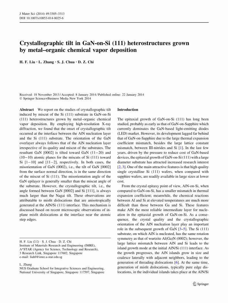
data and their fittings using Eq. (1) are presented in Fig. 6.
The results, together with those of sample B obtained from
Fig. 5, are summarized and compared in Table 2. The
vertical arrows in Fig. 6a, b show that there is an apparent
phase shift in the orientations of the GaN (0002) and Si
(111) of sample A, which has an unintentional Si (111)
miscut toward Si [11-2] direction (see Table 2). The
resultant misorientation of GaN (0002) is toward GaN
[10-10], which is also in the same azimuth as that of Si
[11-2]. However, the crystallographic tilt, i.e., the largest
angle between GaN (0002) and Si (111), occurred in the
GaN [11-20] direction, which is 30� rotated from the
miscut direction of the Si (111) substrate (see Fig. 6a, b).
Finally, for sample C, the situation is quite similar to that
of sample B except for the larger angle of miscut and its
induced GaN (0002) misorientation and tilt (see Table 2).
In Table 2, one can see that the misorientation direction of
GaN (0002) generally follows the miscut direction of Si
(111) and the misorientation angle of GaN (0002) is always
smaller than the miscut angle of the Si (111) substrate (see
the inset of Fig. 5a). It is worth mentioning that this
accurate crystallographic tilt measurement method is also
useful in other epitaxial heterostructures and/or device
fabrications, e.g., polarized GaN-LED [18], where the
orientation of surface polarizer with respect to the crys-
tallographic tilt may have important consequences affect-
ing the light polarization properties.
In epitaxial growth of heterostructures with small lattice
mismatches, a miscut of the substrate, a0S, generally gives
rise to a misorientation of the epilayer, a0E. This is because
the surface of the vicinal substrate contains many atomic
steps with the step height corresponding to the out-of-plane
lattice constant. The lattice mismatch in the growth direc-
tion near the step edges introduces elastic strain into the
heterostructures. The elastic strain decreases with increas-
ing distance away from the step edges, so that the growing
plane is tilted with respect to the substrate in the direction
perpendicular to the surface atomic steps. This phenome-
non was first observed by Nagai in the epitaxial growth of
InGaAs/GaAs heterostructures and can be modeled as [12]
tan aE0
� �¼ �d� tan aS
0
� �; ð2Þ
where d = (cE - cS)/cS, while cE and cS are the out-of-
plane lattice constants (i.e., monolayer thickness) of the
epilayer and the substrate, respectively. a0S is the miscut
angle of the substrate and a0E is the crystallographic tilt
angle, also named as Nagai tilt. Obviously, in this model,
the miscut, the misorientation, and the Nagai tilt are toward
the same direction, which is perpendicular to the surface
atomic steps.
For the GaN-on-Si (111) heterostructures studied here,
the misorientation direction of GaN (0002) summarized in
Table 2 indeed follows that of the miscut direction of Si
(111) in all the samples. However, the crystallographic tilt
direction of sample A is 30� rotated. On the other hand, the
vertical lattice mismatch at the interface of AlN/Si (111) is
-d = 0.2055; in terms of the Nagai model, the miscut
Fig. 5 (color online) a Orientation tilts of GaN (0002) and Si (111)
of the GaN-on-Si (111) heterostructure (sample B) measured by
HRXRD as a function of sample rotations, b differences in the
orientation tilts between Si (111) and GaN (0002) and their alignment
to the /-scan collected from the GaN (10-15) and Si (220) atomic
planes. The solid lines are the best fittings to the experimental data by
using Eq. (1)
3310 J Mater Sci (2014) 49:3305–3313
123
induced Nagai tilt is about a0E & 0.21a0
S. In this regard, the
Nagai tilts of samples A, B, and C should be 0.10�, 0.09�,
and 0.62�, respectively. In fact, we found that these values
are much smaller than those of 0.19�, 0.23�, and 0.79�measured by HRXRD for samples A, B, and C, respec-
tively (see Table 2). Besides, the extended Nagai model for
the case of GaN-on-Si (111), having -d = -0.1917 [11,
19] when compared to the Nagai model (-d = 0.2055),
tends to induce a larger rather than the smaller misorien-
tation angle of the resultant GaN (0002) than the miscut
angle of the Si (111) substrate (see Table 2). Based on the
misorientation directions and the tilt angles discussed
above, we can draw a conclusion that there must be other
factors in the GaN-on-Si (111) heterostructures that con-
tributed to the extra crystallographic tilts and the tilt rota-
tion (typically observed in sample A, see Table 2). As
mentioned above, those misfit dislocations having Burgers
vector components in the direction perpendicular to the
AlN/Si (111) interface must be the main concerns.
It has been reported by Huang et al. [20] that the surface
atomic steps on vicinal substrate of the AlN/SiC hetero-
structure have an important role in relaxing the interfacial
mismatch strain via unpaired partial misfit dislocations. By
employing high-resolution TEM, Litvinov et al. [21]
recently observed misfit dislocations with Burgers vector
parallel to the growth direction at the AlN/Si (111) inter-
face located at the area of Si atomic steps. Such misfit
dislocations, when arranged in a certain direction [22, 23],
e.g., due to atomic step bunching on the surface of vicinal
substrates, [24, 25] will cause significant crystallographic
tilts in the heteroepitaxial growth of GaN-on-Si (111). In
this regard, the rotated tilt (e.g., see sample A shown in
Fig. 6a, b and Table 2) is readily associated with the
anisotropy of dislocation nucleation and/or glide in the
initial growth stage controlled by the bunched atomic steps
on the surface of the vicinal Si (111) substrate. Step bun-
ches and large step-free regions are further confirmed by
AFM on the surface of the GaN-on-Si (111)
heterostructures.
Figure 7a shows the AFM image taken from sample C.
In this sample, the Si (111) substrate has an intentional
miscut of *3� toward Si [1-10] direction. Cross-sectional
TEM revealed that the thickness of the GaN overlayer is
about 1.6 lm, which was grown on an AlN nucleation
layer, separated into 400, 450, 450, and 300 nm sublayers
by three 10 nm thick LT-AlN interlayers. It is clearly seen
Fig. 6 (color online) a,
c Orientation tilts of GaN
(0002) and Si (111) in GaN-on-
Si (111) heterostructures
measured by HRXRD as a
function of sample rotations:
a sample A and c sample C,
b and d differences in the
orientation tilts between Si
(111) and GaN (0002) and their
alignments to the /-scan
collected from the GaN (10-
15) and Si (220) atomic planes:
b sample A and d sample C.
The solid lines are the best
fittings to the experimental data
by using Eq. (1). Rotated tilt is
observed in sample A rather
than sample C as indicated by
the straight arrows
Table 2 Summary and comparisons of the GaN-on-Si (111) hetero-
structure samples aiming at the miscut of the substrate, the misori-
entation of the GaN overlayer, the crystallographic tilt between the
overlayer and the substrate, as well as their directions
Sample Si (111) miscut GaN (0002)
misorientation
Crystallographic
tilt indicated by
GaN
Angle
(�)
Toward Angle
(�)
Toward Angle
(�)
Toward
A 0.46 [11-2] 0.29 [10-10] 0.19 [11-20]
B 0.43 [1-10] 0.21 [11-20] 0.23 [11-20]
C 2.96 [1-10] 2.16 [11-20] 0.79 [11-20]
J Mater Sci (2014) 49:3305–3313 3311
123

in Fig. 7a that the GaN surface structures step down from
top right to bottom left in the AFM image. A section
analysis from the locations indicated by the straight line in
Fig. 7a is shown in Fig. 7b, which clearly reveals flat ter-
races and inclined multiple steps periodically arranged one
after another, i.e., step bunches. The step bunched structure
of the GaN surface is schematically shown in the inset of
Fig. 7b. Following the AFM section analysis in Fig. 7b,
when moving every 1.5 lm along the horizontal axis, the
surface structures increase *50 nm in height. As a result,
the inclined angle between GaN [0001] axis and the surface
normal direction is about 1.9�. Obviously, this AFM
measurement is localized in microscale. The accuracy in
the measured tilt angles is largely depended on the uni-
formity of surface morphology and roughness. In contrast,
the tilt angle measured by HRXRD discussed above is from
an area of 2 9 2 mm2 (defined by the X-ray beam size on
the sample surface). In this light, the tilt angle of sample C
measured by AFM (i.e., 1.9�) is relatively consistent with
the HRXRD result (i.e., 2.16�, see Table 2). The observed
atomic step-bunching effect is believed to affect the
nucleation and/or glide of misfit dislocations that in turn
contributed to the crystallographic tilt and its rotation in the
epitaxial growth of GaN-on-Si (111) heterostructures.
Conclusion
In conclusion, crystallographic tilts have been studied in
various GaN-on-Si (111) heterostructures grown by
MOCVD on unintentional and intentional miscut Si (111)
substrates. It is found that the misorientation direction of the
GaN (0002) atomic planes always follows the miscut
direction of the Si (111) substrate, i.e., perpendicular to the
surface atomic steps. However, the crystallographic tilt, i.e.,
the angle formed between GaN (0002) and Si (111), is
always larger than those derived from the Nagai model and
extended Nagai model. A 30�-rotated tilt is also observed
when the miscut direction of the Si (111) substrate is toward
Si [11-2]. These observations are attributed to the surface
atomic step bunching, which tends to anisotropically locate/
distribute the nucleation and/or glide of misfit dislocations
in the initial growth stage that in turn contributed to the
crystallographic tilt as well as its rotation. Atomic step
bunching on the surface of GaN overlayer has been con-
firmed by AFM in a GaN-on-Si (111) heterostructure with
the Si (111) miscut of *3�; meanwhile, a tilt angle of 1.9�between GaN (0002) and the surface normal direction (i.e.,
misorientation) is derived from the AFM image via section
analysis, which is relatively consistent with the value of
2.16� obtained by HRXRD. We also found that the crystal
orientation of the GaN overlayer always follows that of the
AlN nucleation layer regardless of the crystal qualities of
the nucleation layer, the materials and structures of the
buffer layer, and the angles and directions of the miscut.
Acknowledgements The authors would like to thank C. B. Soh, S.
Tripathy, and K. Y. Zang for sharing the GaN-on-Si (111) hetero-
structure samples.
References
1. Dadgar A, Schulze F, Wienecke M, Gadanecz A, Blasing J, Veit
P, Hempel T, Diez A, Christen J, Krost A (2007) Epitaxy of GaN
on silicon—impact of symmetry and surface reconstruction. New
J Phys 9:389
Fig. 7 (color online) a AFM image (5.7 lm 9 5.7 lm) recorded
from the surface of the GaN-on-Si (111) heterostructure sample C,
b A sectional analysis of the surface structures observed in (a). The
straight line in (a) indicates the locations for the section analysis and
the inset in (b) is a schematic geometry of the step bunched surface
structures
3312 J Mater Sci (2014) 49:3305–3313
123

2. Chung JW, Ryu K, Liu B, Palacios T (2010) IEEE solid-state
device research conference (ESSDERC). In: Proceedings of the
European, pp 52–56
3. Zhu D, McAleese C, McLaughlin KK, Haberlen M, Salcianu CO,
Thrush EJ, Kappers MJ, Phillips WA, Lane P, Wallis DJ, Martin
T, Astles M, Thomas S, Pakes A, Heuken M, Humphreys CJ
(2009) GaN-based LEDs grown on 6-inch diameter Si (111)
substrates by MOVPE. Proc SPIE 7231:723118
4. Drechsel P, Stauss P, Bergbauer W, Rode P, Fritze S, Krost A,
Markurt T, Schulz T, Albrecht M, Riechert H, Steegmuller U
(2012) Impact of buffer growth on crystalline quality of GaN
grown on Si(111) substrates. Phys Status Solidi A 209:427
5. Krost A, Dadgar A (2002) GaN-based optoelectronics on silicon
substrates. Mater Sci Eng B 93:77
6. Taniyasu Y, Kasu M, Makimoto T (2007) Threading dislocations
in heteroepitaxial AlN layer grown by MOVPE on SiC (0 0 0 1)
substrate. J Cryst Growth 298:310
7. Dodson BW, Myers DR, Datye AK, Kaushik VS, Kendall DL,
Martinez-Tovar B (1988) Asymmetric tilt boundaries and gen-
eralized heteroepitaxy. Phys Rev Lett 61:2681
8. Matyi RJ, Lee JW, Schaake HF (1988) Substrate orientation and
processing effects on GaAs/Si misorientation in GaAs-on-Si
grown by MBE. J Electron Mater 17:87
9. Contreras O, Ponce FA, Christen J, Dadgar A, Krost A (2002)
Dislocation annihilation by silicon delta-doping in GaN epitaxy
on Si. Appl Phys Lett 81:4712
10. Suda J, Miyake H, Amari K, Nakano Y, Kimoto T (2009) Sys-
tematic investigation of c-axis tilt in GaN and AlGaN grown on
vicinal SiC(0001) substrates. Jpn J Appl Phys 48:020202
11. Huang XR, Bai J, Dudley M, Dupuis RD, Chowdhury U (2005)
Epitaxial tilting of GaN grown on vicinal surfaces of sapphire.
Appl Phys Lett 86:211916
12. Nagai H (1974) Structure of vapor-deposited GaxIn1-x as crys-
tals. J Appl Phys 45:3789
13. Liu HF, Dolmanan SB, Zhang L, Chua SJ, Chi DZ, Heuken M,
Tripathy S (2013) Influence of stress on structural properties of
AlGaN/GaN high electron mobility transistor layers grown on
150 mm diameter Si (111) substrate. J Appl Phys 113:023510
14. Pesek A, Hingerl K, Riesz F, Lischka K (1991) Lattice misfit and
relative tilt of lattice planes in semiconductor heterostructures.
Semicond Sci Technol 6:705
15. Liu HF, Tan CC, Dalapati GK, Chi DZ (2012) Magnetron-sputter
deposition of high-indium-content n-AlInN thin film on p-Si(001)
substrate for photovoltaic applications. J Appl Phys 112:063114
16. Liu HF, Dolmanan SB, Tripathy S, Dalapati GK, Tan CC, Chi
DZ (2013) Effects of A1N thickness on structural and transport
properties of In-rich n-AlInN/AlN/p-Si(0 0 1) heterojunctions
grown by magnetron sputtering. J Phys D 46:095106
17. Liu HF, Chua SJ, Hu GX, Gong H, Xiang N (2007) Effects of
substrate on the structure and orientation of ZnO thin film grown
by rf-magnetron sputtering. J Appl Phys 102:083529
18. Zhang L, Teng JH, Chua SJ, Fitzgerald EA (2009) Linearly
polarized light emission from InGaN light emitting diode with
subwavelength metallic nanograting. Appl Phys Lett 95:261110
19. Kim TH, Baek SH, Jang SY, Yang SM, Chang SH, Song TK,
Yoon J-G, Eom CB, Chung J-S, Noh TW (2011) Step bunching-
induced vertical lattice mismatch and crystallographic tilt in
vicinal BiFeO3(001) films. Appl Phys Lett 98:022904
20. Huang XR, Bai J, Dudley M, Wagner B, Davis RF, Zhu Y (2005)
Step-controlled strain relaxation in the vicinal surface epitaxy of
nitrides. Phys Rev Lett 95:086101
21. Litvinov D, Gerthsen D, Vohringer R, Hu DZ, Schaadt MD
(2012) Transmission electron microscopy investigation of AlN
growth on Si(111). J Cryst Growth 338:283
22. Sakai A, sunakawa H, Usui A (1998) Transmission electron
microscopy of defects in GaN films formed by epitaxial lateral
overgrowth. Appl Phys Lett 73:481
23. Barabash RI, Roder C, Ice GE, Einfeldt S, Budai JD, Barabash
OM, Figge S, Hommel D (2006) Spatially resolved distribution of
dislocations and crystallographic tilts in GaN layers grown on
Si(111) substrates by maskless cantilever epitaxy. J Appl Phys
100:053103
24. Degawa M, Minoda H, Tanishiro Y, Yagi K (1999) Temperature
dependence of period of step wandering formed on Si(111) vic-
inal surfaces by DC heating. J Phys 11:L551
25. Ramana Mutry MV, Fini P, Stephenson GB, Thompson C,
Eastman JA, Munkholm A, Auciello O, Jothilingam R, DenBaars
SP, Speck JS (2000) Step bunching on the vicinal GaN(0001)
surface. Phys Rev B 62:R10661
J Mater Sci (2014) 49:3305–3313 3313
123