crystallization of small molecules for organic electronic applications jessica lynn saylors, anna...
Post on 19-Dec-2015
217 views
TRANSCRIPT

Crystallization of Small Molecules for Organic Electronic
ApplicationsJessica Lynn Saylors, Anna Hiszpanski, and Yueh-Lin (Lynn)
Loo
07 October 2011Summer of Learning Symposium 2011
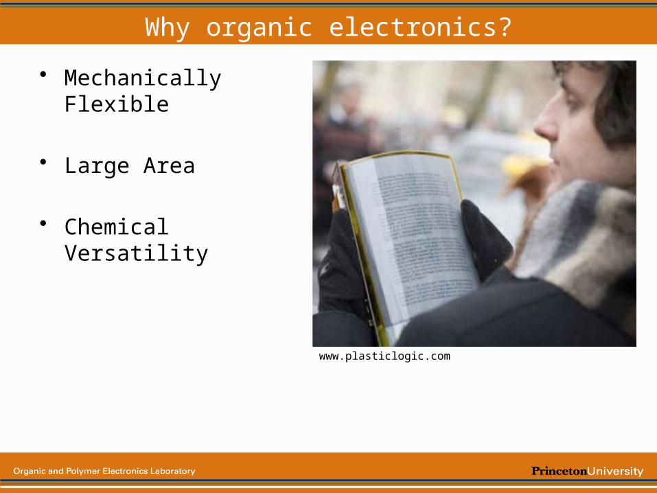
Why organic electronics?
• Mechanically Flexible
• Large Area
• Chemical Versatility
www.plasticlogic.com

Transistors – Building Blocks of Organic Electronics
organic semiconductor
gate + dielectric
source
drain
How an Transistor works
S D
Organic
Insulator
Gate electrode
0 V 0 V 0 V -1 V 0 V -5 V
0 V -5 V -5 V
- - - - - - - - -+ + + + + + + + +
- - - - - - - - -+ + + + + + + + + + + + + + +
+ +
- - - - - - - - -+ + + + + + + + +- - - - - -
Cut-off regime
Linear regime Saturation regime
Organic field-effect transistor (OFET)

Xiao, S. et al. Angew. Chem. Int. Ed. 2005.
Contorted Hexabenzocoronene
(HBC)
HBC
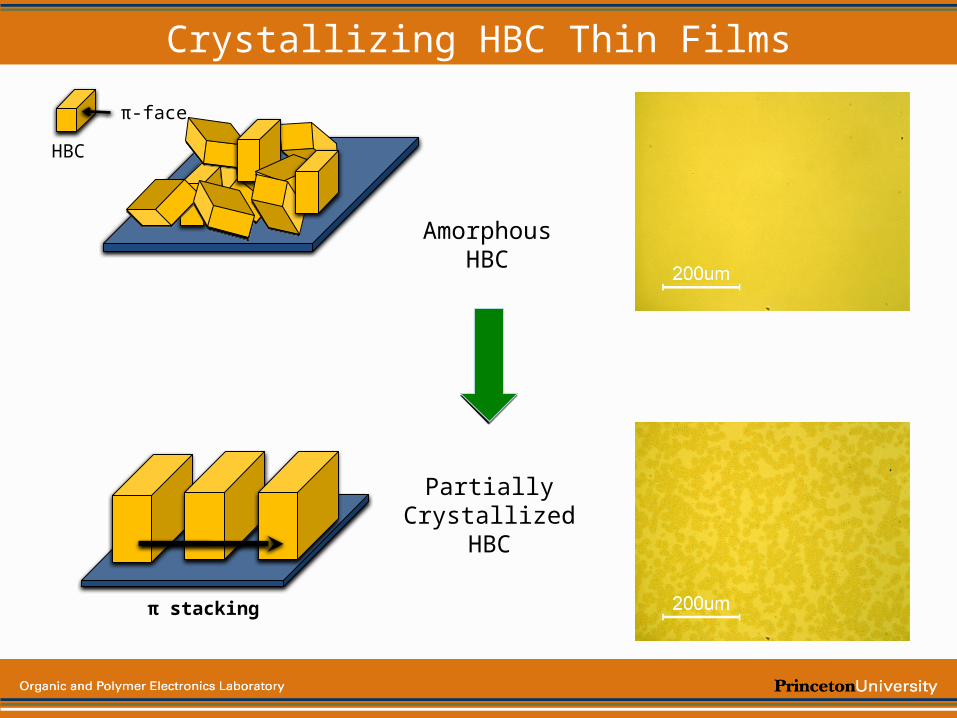
Crystallizing HBC Thin Films
π stacking
π-face
HBC
Amorphous HBC
Partially Crystallized HBC
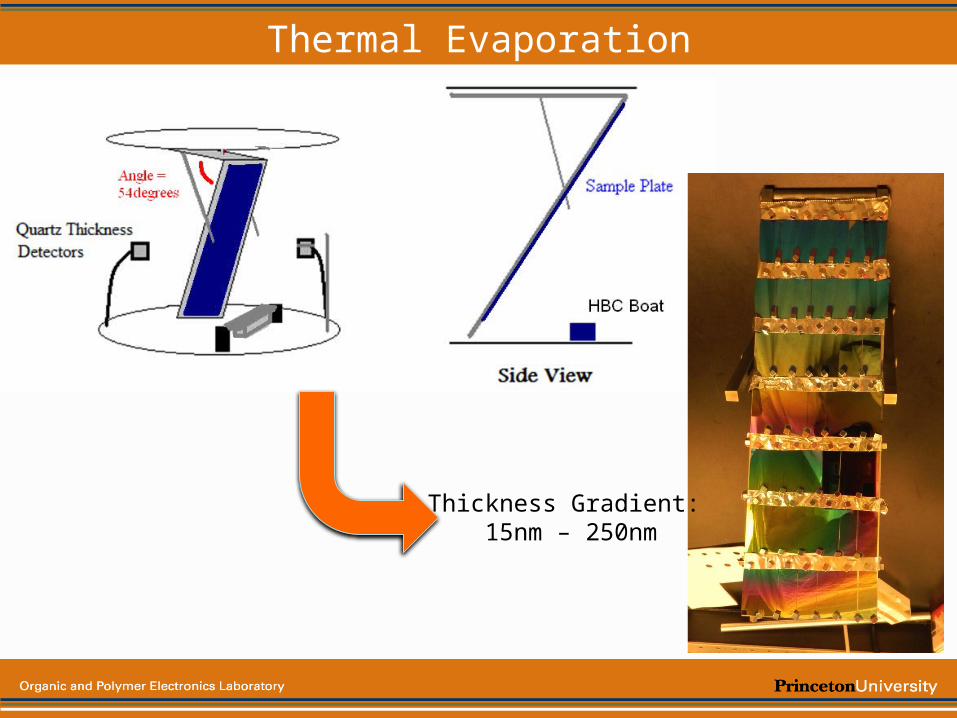
Thermal Evaporation
Thickness Gradient: 15nm – 250nm
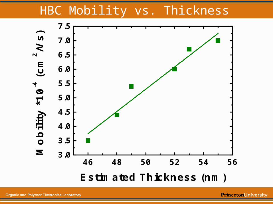
HBC Mobility vs. Thickness
46 48 50 52 54 563.0
3.5
4.0
4.5
5.0
5.5
6.0
6.5
7.0
7.5
Mo
bil
ity
*1
0-4 (
cm
2 /Vs
)
Estimated Thickness (nm)
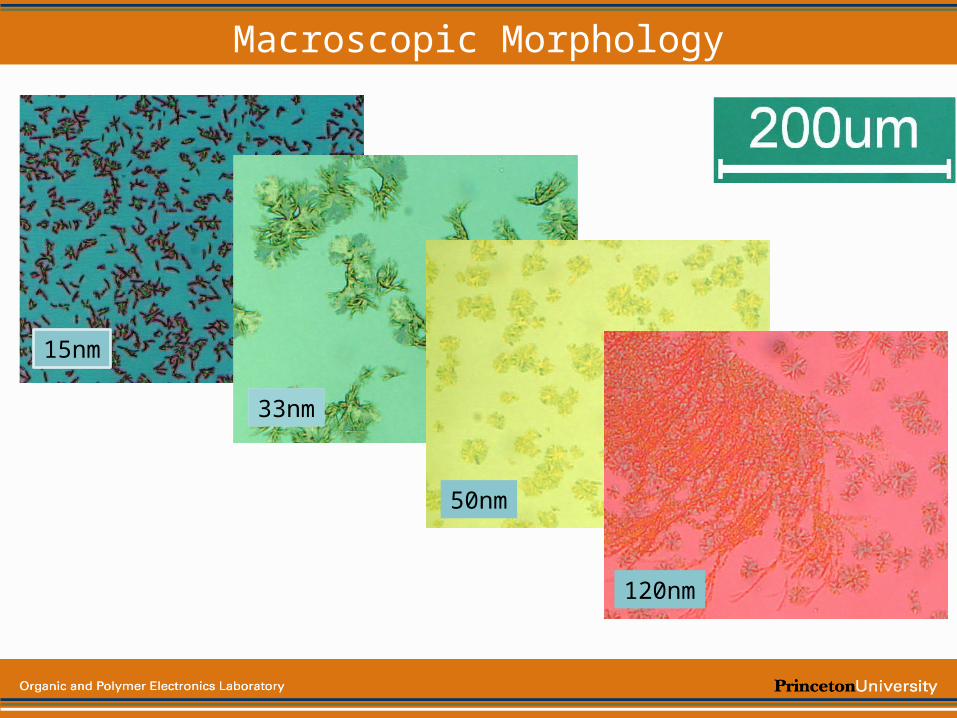
Macroscopic Morphology
15nm
33nm
50nm
120nm
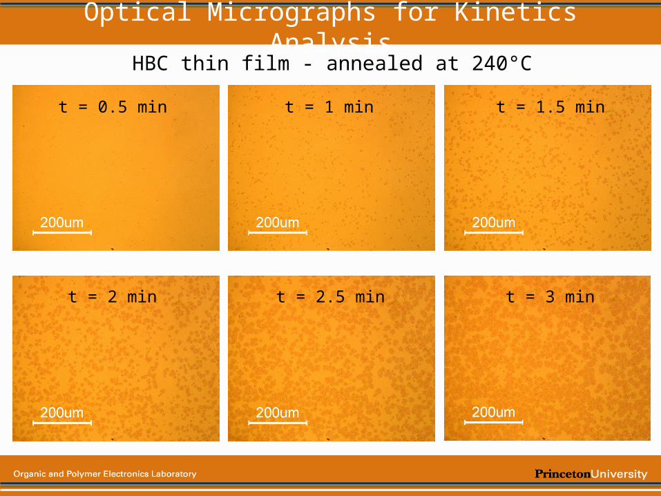
Optical Micrographs for Kinetics AnalysisHBC thin film - annealed at 240°C
t = 0.5 min t = 1 min t = 1.5 min
t = 2 min t = 2.5 min t = 3 min

Avrami Kinetics
n: variable that gives some indication
regarding mode of crystallization
K: indication of therate of crystallization
%crystallized

0 20 40 60 80 100 120 140 160 180
0.5
1.0
1.5
2.0
2.5
3.0
3.5
227C 240C 255C
n
Thickness (nm)
Avrami n vs. Thickness

0 20 40 60 80 100 120 140 160 180
0.5
1.0
1.5
2.0
2.5
3.0
3.5
227C 240C 255C
n
Thickness (nm)
Avrami n vs. Thickness

American Institute of Chemical Engineers
http://www.aiche.org/Students/Conferences/national.aspx
http://www.minneapolisconventioncenter.com/

Acknowledgments
• Loo Group– Anna Hiszpanski– Professor Loo
• Princeton Environmental Institute
• Siebel Energy Grand Challenge
http://www.princeton.edu/pei/
Loo Group, March 2011