crystalline silicon solar cell technology - kurt j. lesker... · pdf filecrystalline silicon...
TRANSCRIPT

Rubin Sidhu, David E. CarlsonBP Solar
April 13, 2010
Crystalline Silicon Solar Cell Technology

Agenda
• Global PV Market• Nomenclature• PV Technologies• Crystalline Silicon Solar Cell Value Chain• Solar Cell Physics (no equations!)
• Why is solar cell efficiency only ~15%?• Reaching Grid Parity using BP Solar’s Crystalline
Silicon PV Technology• The Solar America Initiative• Silicon Solar Technology Roadmap
• Conclusion: Future of PV

PV Experience Curve
Cost of Materials Limit (20% Modules)Cost of Materials Limit (20% Modules)Cost of Materials Limit (20% Modules)Cost of Materials Limit (20% Modules)Cost of Materials Limit (20% Modules)Cost of Materials Limit (20% Modules)
PV module prices have followed an experience curve with a slope PV module prices have followed an experience curve with a slope of of ~ 80% ~ 80%
20% decrease in price with every doubling of cumulative producti20% decrease in price with every doubling of cumulative productionon

Cost of Solar Electricity

Shipments of Photovoltaic Modules
Projection (Lux Research)
PV shipments actually increased about 20% 2009.

PV Shipments & Countries of Origin
(Navigant Consulting)
Europe has been the largest consumer of PV in recent years (> 50% of all installations). China and Taiwan have become the largest producers.
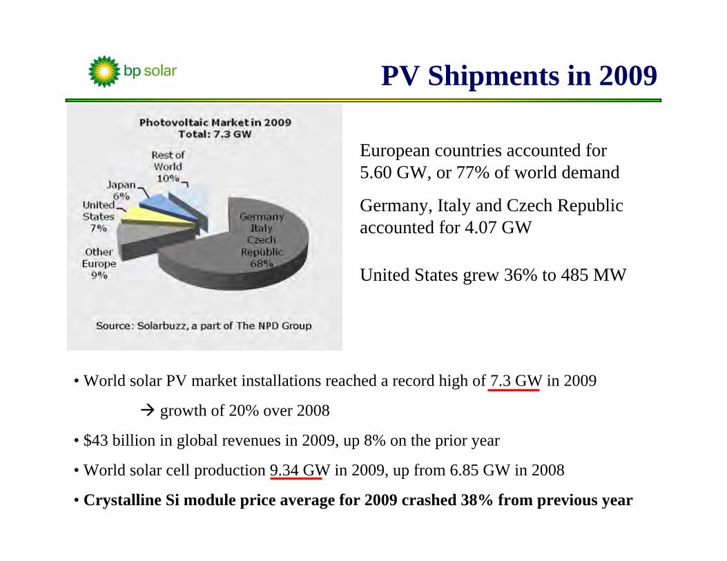
PV Shipments in 2009
• World solar PV market installations reached a record high of 7.3 GW in 2009
growth of 20% over 2008
• $43 billion in global revenues in 2009, up 8% on the prior year
• World solar cell production 9.34 GW in 2009, up from 6.85 GW in 2008
• Crystalline Si module price average for 2009 crashed 38% from previous year
European countries accounted for 5.60 GW, or 77% of world demand
Germany, Italy and Czech Republic accounted for 4.07 GW
United States grew 36% to 485 MW

Grid Parity
GTM Research

LCOE and kWh/kWp
Levelized Cost Of Electricity (¢/kWh):LCOE is the minimum price at which energy must be sold for
an energy project to break even
Including: initial investment operations and maint. cost of fuel cost of capital
Typical Sunny Day
0
200
400
600
800
1000
1200
0 6 12 18 24
(W/m
²)
7.5 Sun-Hour Day24-Hour Equivalent
7.5 kWh Spread over 24 Hours
6 AM Noon 6 PM

Insolation
kWh/kWp

PV Facts
Using today’s PV Technology, an array field that is 300 miles on each side could produce the entire electrical energy used by the United States in a year.

PV Facts
Over its lifetime, a typical PV module, in a sunny climate, will produce over twenty times the electricity initially used to manufacture it.

Technology Overview: Nomenclature
A solar PV cell is the smallest semiconductor device that can convert sunlight into electrical energy
A module is an assembly of cells in series or parallel to augment voltage and/or current
A panel is an assembly of modules on a structure
An Array is an assembly of panels at a site.
Multi (Poly) Cell Mono Cell
Large Roof-Top PV Array

Conversion Efficiencies vs. Time (NREL)
There has been steady progress in the improvement of conversion efficiencies for a number of PV technologies over the last few decades.

The Major Players
Sharp SolarPower Kyocera BP Solar Q-Cells Mitsubishi SolarWorld Panasonic (Sanyo) Schott Solar Isofoton Motech Suntech Evergreen Solar JA Solar
United Solar Kaneka Fuji Electric Sharp Mitsubisihi Schott Solar SunTech EPV PowerFilm AMAT licensees Orelikon licenses
Nanosolar Avancis Solar Frontier Wurth Solar Global Solar Honda Soltec
First Solar Antec Solar Abound Solar PrimeStar Solar Calyxo
Crystalline Si a-Si/µc-Si CIGS CdTe
There are currently more than 300 companies developing or producing solar cells.
With prices continuing to decrease, and more companies entering the market, many small companies and start-ups are likely to fail.

Source: pvsociety

Manufacturing Process for mc-Si PV Modules
% of % of % of % ofTotal Total Total Total0.00% 0.00% 0.00% 0.00%0.27% 2.03% 0.34% 0.85%2.18% 13.23% 2.23% 2.53%
SIZING WAFERING
FINISHTEST
INTER-CONNECTLAMINATION
ANTI-REFLECTIVECOATING
CLEANINGCASTING DIFFUSION
METALLIZATION
% of % of % of % ofTotal Total Total Total0.00% 0.00% 0.00% 0.00%0.27% 2.03% 0.34% 0.85%2.18% 13.23% 2.23% 2.53%
SIZING WAFERING
FINISHTEST
INTER-CONNECTLAMINATION
ANTI-REFLECTIVECOATING
CLEANINGCASTING DIFFUSION
METALLIZATION
Most companies are manufacturing PV modules based on screen-printing contacts on multicrystalline silicon wafers

CZ - Silicon for Solar
Silicon Feedstock
Mono solar cell
Mono-crystalline wafer Drawbacks of CZ Solar
– Cylindrical ingot (module packing)
– Smaller throughput rate• CZ: 5.3 kg/h at 2mm/min• Cast: 12.9 kg/h at 0.3mm/min
– High oxygen content -> LID– Higher energy use– Feedstock limitations– Importance of skilled operators
Mono module

Multicrystalline Silicon Casting
Silicon Feedstock
Silicon Ingot
Silicon Bricks
Multi-crystalline
Wafer
Multicrystalline Solar Cell
Multicrystalline Module
Casting Station cross-section
Heater
Crucible Liquid Si
Solid Si
Insulation
Drawbacks:• Crystal defects
• Iron from crucible
• Inclusions from coating, furnace
• Not compatible with pyramid texturing
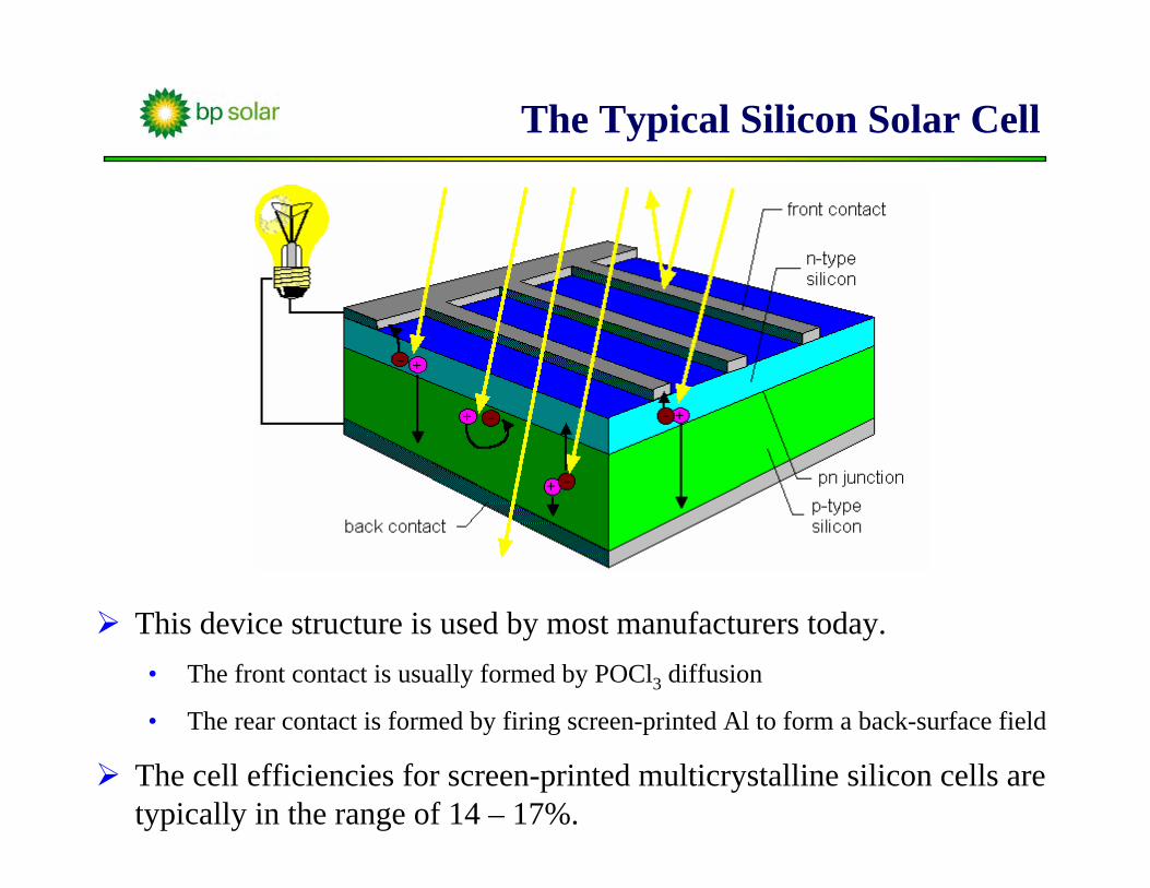
The Typical Silicon Solar Cell
This device structure is used by most manufacturers today.• The front contact is usually formed by POCl3 diffusion
• The rear contact is formed by firing screen-printed Al to form a back-surface field
The cell efficiencies for screen-printed multicrystalline silicon cells are typically in the range of 14 – 17%.

Operation of a Solar Cell
The theoretical limit for a crystalline silicon solar cell is ~ The theoretical limit for a crystalline silicon solar cell is ~ 29%.29%.
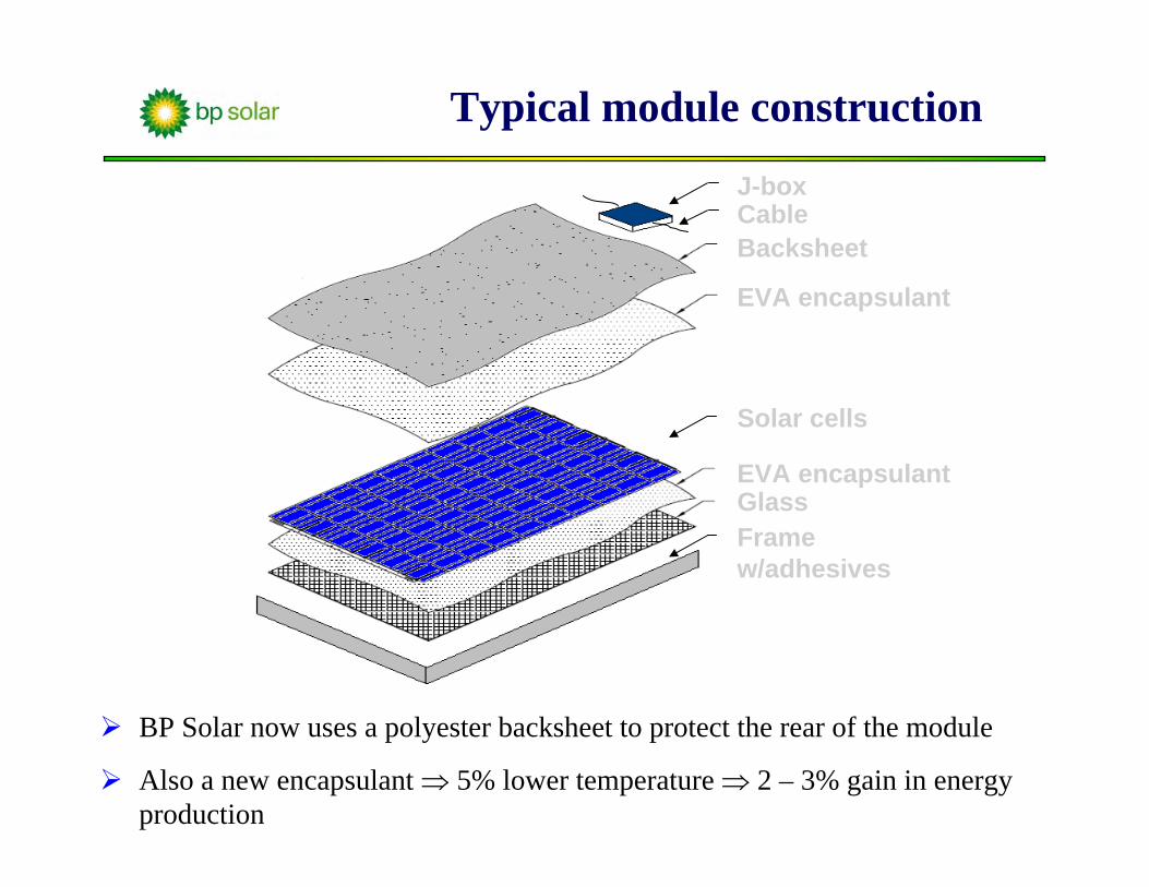
Backsheet
EVA encapsulant
Solar cells
EVA encapsulantGlass
J-boxCable
Frame w/adhesives
Typical module construction
BP Solar now uses a polyester backsheet to protect the rear of the module
Also a new encapsulant 5% lower temperature 2 – 3% gain in energy production

PV Module Costs
Silicon 23%
Other Materials 27%Labor 25%
Equipment 15%
Electricity 10%
Si Wafer PV Module Production Cost $2.10/W
Major Energy Consuming Steps
Feedstock 3%
Ingot 3%
Wafering 2%
Cell 2%
Silicon 23%
Other Materials 27%Labor 25%
Equipment 15%
Electricity 10%
Si Wafer PV Module Production Cost $2.10/W
Major Energy Consuming Steps
Feedstock 3%
Ingot 3%
Wafering 2%
Cell 2%
About half of the total module cost is associated with the cost of materials
Silicon prices have been dropping rapidly over the last 18 months
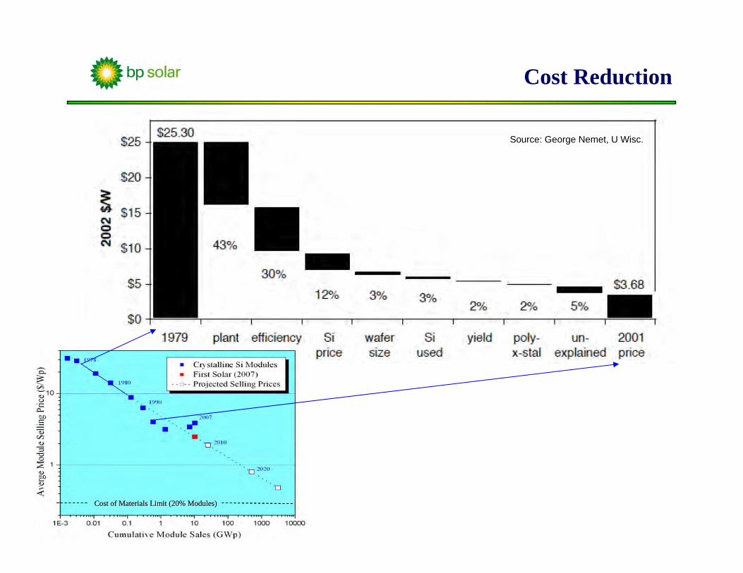
Source: George Nemet, U Wisc.
Cost of Materials Limit (20% Modules)Cost of Materials Limit (20% Modules)Cost of Materials Limit (20% Modules)Cost of Materials Limit (20% Modules)Cost of Materials Limit (20% Modules)Cost of Materials Limit (20% Modules)
Cost Reduction

Solar America Initiative
This program is a BP Solar cost shared Technology Pathways Partnership under the DOE Solar Energy Program.
The program addresses all aspects of crystalline silicon PV manufacturing and systems deployment.
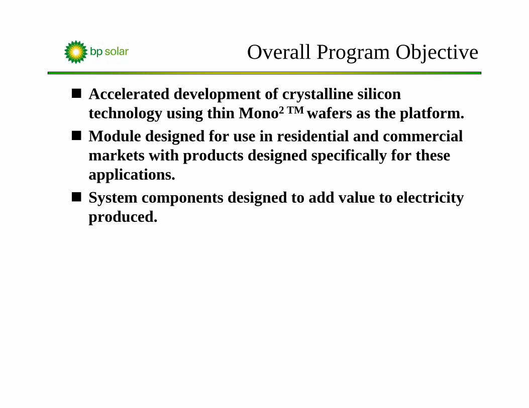
Overall Program Objective
Accelerated development of crystalline silicon technology using thin Mono2 TM wafers as the platform.
Module designed for use in residential and commercial markets with products designed specifically for these applications.
System components designed to add value to electricity produced.

PV Product Value Chain
Metallurgical Silicon
Semi-conductor Silicon
Crystal Growth
Wafering Cell Fabrication
Module Assembly

Mono2 TM Silicon Casting
Silicon Feedstock
Silicon Ingot
Silicon BricksCasting Station cross-section
Heater
Crucible Liquid Si
Solid Si
Insulation
Mono2
WaferMono2
Solar CellMono2
Module

Mono2 TM Lifetime Uniformity
61934.7116.4175 s40%
Mono2 TM, pyramid etched
61833.5515.8775 s40%
Mono2 TM
61033.1515.4675 s80%
Multi
VocmV
JscmA/cm2
%
Lifetime Median
Std. Dev.
Material
Simulation results
Multi
Mono2 TM

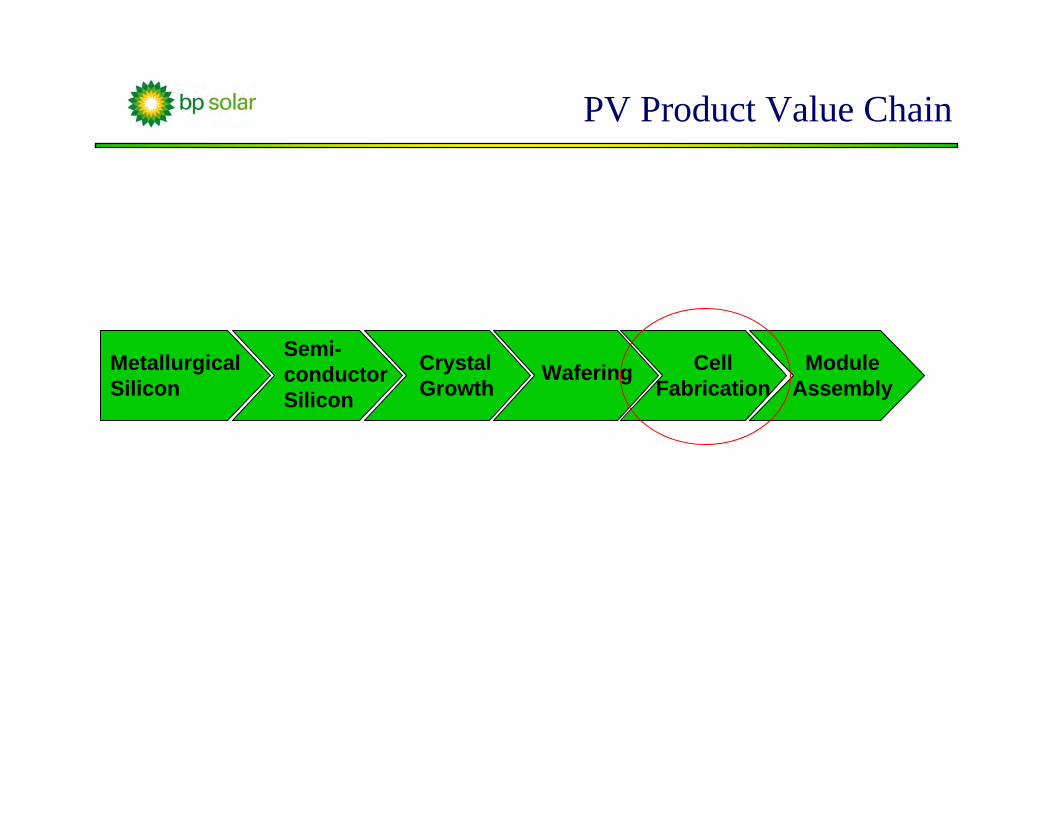
PV Product Value Chain
Metallurgical Silicon
Semi-conductor Silicon
Crystal Growth
Wafering Cell Fabrication
Module Assembly

c-Si Solar Cells: Loss Mechanisms
0.7%
2.4%
2.2%
2.5%
6.3%
ReflectionShadowingOther (Optical)OhmicRecombination
Thermodynamic limit forcrystalline Si solar cells ~29%
Sources of loss relative tomaximum achievable efficiency– Front surface reflection– Emitter contact shadowing– Poor rear reflectance for light
trapping– Surface recombination (i.e.,
surface cleanliness)– Bulk recombination (i.e.,
material quality)– Resistive losses at the cell
and module level

Cell Process
Texture Etch– ICT
o Preferred option for Mono2 and multi o Cell efficiency improvements demonstratedo Improvements lost when cells are encapsulated
– Alkaline texture etcho Good for Mono2 but not multio Increased cell and module efficiencies by ~ 0.5% absolute.

Cell Process
Back Print Optimization– Maximize area covered with Al paste for improved
performance– Minimize area of Ag pads to reduce cost– Implemented new pattern in production with 0.6% gain in cell
efficiency and 1% increase in module efficiency.
Advanced Metallization– Looking at new approaches to increase metallization thickness,
to reduce series resistance while also reducing finger width andtherefore shadowing.
– Looking at aerosol jet printing, ink jet printing and offset printing.
– Successfully printed 80 to 90 µm wide and ~ 35 µm thick

c-Si Solar Cells: Advances
Source: pvsociety

The Selective Emitter
A number of organizations are developing solar cells with selective emitters in order to use thinner emitters and improve the short-wavelength spectral response.

Passivated Rear Point Contacts
Fraunhofer ISE has used laser firing of aluminum to fabricate high efficiency (21.7%) solar cells with passivated rear point contacts.

The PERL Solar Cell
p p-silicon
n
p
p
oxide
+
+p ++
n +
rear contact oxide
PERL Cell Structure
p p-silicon
n
p
p
oxide
+
+p ++
n +
rear contact oxide
PERL Cell Structure
The PERL solar cell has a passivated emitter with a rear locally diffused base contact, and efficiencies as high as 25% have beenobtained with this structure.

SunPower Back Contact Solar Cell
The SunPower cell has all its electrical contacts on the rear surface of the cell.
Production cells ~ 22.4% efficiency; new prototypes at 23.4%.
Diffusion lengths > 3 x cell thickness (using 145 m thick CZ-Si at end of 2008).

Sanyo HIT Solar Cell
The HIT cell utilizes amorphous Si intrinsic layers (~ 5 nm) as passivation layers. The cell is symmetric except for the a-Si p+ emitter layer (~ 10 nm) on the front and the a-Si n+ contact layer (~ 15 nm) on the rear.
Best lab efficiency = 22.3% (open-circuit voltages as high as 739 mV).

PV Product Value Chain
Module Assembly defines product reliability and longevity
Material choice is key to meet life time goal Good choice of materials allows life time to exceed
warranty period Balance of performance and cost
Metallurgical Silicon
Semi-conductor Silicon
Crystal Growth
Wafering Cell Fabrication
Module Assembly

Module Packaging Materials
Encapsulant: Glue for the whole package: Key component
Back sheet: Protect cells against the environment and provide electrical isolation
Superstrate glass: Cell protection and light capture Frames and framing adhesives: Mounting and load
bearing J-box/Cables: Electric isolation and longevity Tabbing ribbons: For cell interconnection

Module Development
AR Coated Glass– Qualified and implemented Gen 1 AGC Flat Glass NA AR
coated glass with 1.5 to 2% increase in STC power and 4% increase in overall energy collection
– Gen 2 now under development with improved cosmetic uniformity and ~ 2.5% STC power gain.
EVA cure level determination– Standard approach is to use chemical extraction of un-cross
linked EVA (gel content)– Developed differential scanning calorimetry (DSC) as a fast
and reliable way of measuring cross-link density.

ARC vs. standard module
Normalized energy generation of a day– 6% to 7% more energy at early and late periods of the day
-1%
1%
3%
5%
7%
9%
6:00 7:00 8:00 9:00 10:00 11:00 12:00 13:00 14:00 15:00 16:00 17:00
Time of Day
kWh/
kWp
diffe
renc
e be
twee
n A
R c
oate
d &
Unc
oate
d gl
ass
Perc
enta
ge k
Wh/
kWp
diff
eren
ce
Time of Day-1%
1%
3%
5%
7%
9%
6:00 7:00 8:00 9:00 10:00 11:00 12:00 13:00 14:00 15:00 16:00 17:00
Time of Day
kWh/
kWp
diffe
renc
e be
twee
n A
R c
oate
d &
Unc
oate
d gl
ass
Perc
enta
ge k
Wh/
kWp
diff
eren
ce
Time of Day
Standard modules
AR coated modules
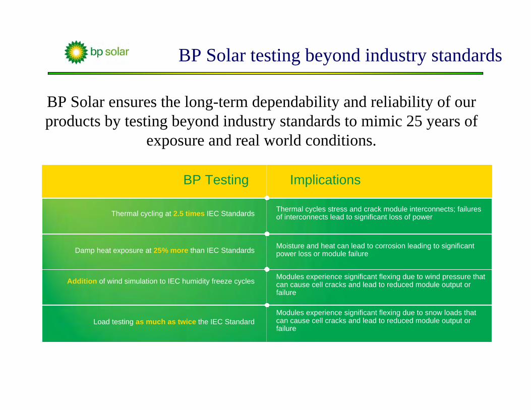
BP Solar testing beyond industry standards
BP Solar ensures the long-term dependability and reliability of our products by testing beyond industry standards to mimic 25 years of
exposure and real world conditions.
BP Testing Implications
Thermal cycling at 2.5 times IEC Standards
Damp heat exposure at 25% more than IEC Standards
Addition of wind simulation to IEC humidity freeze cycles
Load testing as much as twice the IEC Standard
Thermal cycles stress and crack module interconnects; failures of interconnects lead to significant loss of power
Moisture and heat can lead to corrosion leading to significant power loss or module failure
Modules experience significant flexing due to wind pressure thatcan cause cell cracks and lead to reduced module output or failure
Modules experience significant flexing due to snow loads that can cause cell cracks and lead to reduced module output or failure

Residential Building-Integrated PV
Building-integrated PV may become ubiquitous in the next few decades.

Large Grid-Connected PV Arrays
The levelized cost of electricity should fall to ~ 6 ¢/kWh by 2015 for large grid-connected arrays

Solar Energy – the Long-Term Solution?
Source: German Advisory Council on Global Change
Some forecasts predict that solar will provide most of our energy needs in the latter half of this century.

Projections for the Future of PV
The levelized cost of PV electricity could fall to ~ 6 ¢/kWh by 2015
Disruptive technologies with theoretical limits of > 60% may emerge in the next few decades
Assuming a CAGR of 35% (average over the last few decades), the cumulative PV production would be ~ 3.5 TWp by 2026.
3 TWp of solar electricity will reduce carbon emissions by about 1 Gton per year (7 Gtons of carbon were emitted as CO2in 2000)
Thus, by about 2030 PV could be producing about 10% of the world’s electricity and start to play a major role in reducing CO2 emissions

Questions?