crystal growth of cu2znsns4 by chemical vapour transport
TRANSCRIPT
Crystal growth of Cu2ZnSnS4 Solar Cell Absorber by Chemical Vapour Transport with I2
D. Colombara1*
, S. Delsante2, G. Borzone
2, J. M. Mitchels
3, K. C. Molloy
4, L. H. Thomas
4, B. G.
Mendis5, C. Y. Cummings
6, F. Marken
4 and L. M. Peter
4
1*
Université du Luxembourg – 41, rue du Brill - L-4422 Belvaux, Luxembourg 2Università degli Studi di Genova – DCCI, via Dodecaneso 31 - 16146 Genova, Italy
3University of Bath – Microscopy and Analysis Suite, Bath BA2 7AY, United Kingdom
4University of Bath – Department of Chemistry, Bath BA2 7AY, United Kingdom.
5Durham University – Department of Physics, Durham DH1 3LE, United Kingdom
6University of Southampton – Department of Chemistry, Southampton SO17 1BJ, United Kingdom
Email [email protected]
Abstract
Single crystals of Cu2ZnSnS4 have been produced within sealed quartz ampoules via the chemical
vapour transport technique using I2 as the transporting agent. The effects of temperature gradient and I2
load on the crystal habit and composition are considered. Crystals have been analysed with XRD,
SEM, and TEM for compositional and structural uniformities at both microscopic and nanoscopic
levels. The synthesized crystals have suitable (I2-load dependent) properties and are useful for further
solar absorber structural and physical characterizations. A new chemical vapour transport method
based on longitudinally isothermal treatments is attempted. Based on a proposed simplistic mechanism
of crystal growth, conditions for crystal enlargement with the new method are envisaged.
Keywords: B1. CZTS; B1. Kesterite; B2. Semiconducting quaternary chalcogenide; B3. Solar cell
absorber; A2. Iodide vapour transport; A2. Transversal chemical vapour transport; A1. Congruent
transport.
1. Introduction
In the frame of the thin film solar cells research area a new absorber compound has lately [1] gained
interest due to its non-toxic low cost elemental constituents: Cu2ZnSnS4 (CZTS). Very promising
results have recently been obtained on photovoltaic devices based on related sulfoselenide compounds
deposited with an ink-based approach [2, 3], suggesting that this material might soon become
competitive with Cu(In,Ga)(S,Se)2 and CdTe for the production of commercial modules, due to the
toxicity/availability issues affecting Cd, Te, Ga and In [4-6]. Although many studies are being
performed on thin films of this material, some key questions can only be answered by studying single
crystalline forms: crystal and electronic structures [7], phonon frequencies and line widths of Raman
active modes and extension of the compositional homogeneity range [8]. It is therefore important to
develop improved crystal growth methods.
Olekseyuk et al. [9] have found that Cu2ZnSnS4 melts incongruently at 1253K, crystallizing by the
peritectic reaction p4: L + β’ (ZnS) → δ (Cu2ZnSnS4) with a composition of the liquid phase (L) far
poor in ZnS and rich in Cu2SnS3. As a consequence it was found by Shimada et al. [10] that the crystal
growth of Cu2ZnSnS4 from the melt results in the presence of impurity phases such as Cu2SnS3, ZnS
and SnS, besides the quaternary chalcogenide, probably owing to segregation during the crystallization
process. The solidification of a single-phase CZTS from the stoichiometric melt might be improved to
some extent by the presence of a suitable seed or the action of a directional cooling, like in the
Czochralski, the Bridgman-Stockbarger [11] or the gradient freezing techniques [12]. Single crystals of
the Cu2FeSnS4-Cu2ZnSnS4 pseudobinary series were synthesized by Bernardini et al. [13] for structural
investigations using the salt-flux technique reported by Moh et al. [14]. A similar approach was also
employed by Altosaar et al. [15] and Timmo et al. [16] who successfully crystallized Cu2Zn1-xCdx
Sn(Se1-ySy)4 and Cu2ZnSnSe4-xSx powders from molten KI with the intent of fabricating monograin
layer devices [17]. The difficulty of producing the sulfur end member in a pure form was highlighted,
since the X-ray Energy Dispersive Spectroscopy (EDS) analysis of the polished crystals pointed to the
presence of the secondary phases alongside the dominating CZTS phase. At the time of writing this
manuscript Nagaoka et al. [18] have demonstrated the possibility to obtain primary CZTS crystals by a
Sn-poor liquid phase in the Sn-Cu2ZnSnS4 pseudobinary system at 900 °C. CZTS single crystals of
reasonable dimensions were first produced by Nitsche et al. [19] with the Chemical Vapour Transport
(CVT) technique employing I2 as the transporting agent (with low loading); the crystals were reported
to be black needles with dimensions of up to 20 mm x 0.2 mm x 0.2 mm. Compositional analysis was
not reported, but structure refinement from X-Ray Diffraction (XRD) revealed the compound to
crystallize in a tetragonal lattice with a = b = 5.427 Å and c = 10.848 Å [20]. Nitsche’s CVT results
have only now been outclassed in terms of crystal thickness by Levcenko et al. [21] who succeeded in
growing black blade shape crystals up to 5 mm x 1.5 mm x 1 mm.
Among the techniques for the growth of single crystals, the CVT has generally the advantage of
employing lower operational temperatures and static configurations of the growing ampoule, the main
drawbacks being the incorporation of the gaseous solvent species to some extent and the sensitivity of
the technique to subtle variations of the growth conditions. The importance of fluid dynamics in
determining the right growth conditions in such systems is well described by the literature [22-32]. The
CVT crystal grower will often encounter dimensionless numbers such as the Grashof, Schmidt, Prandtl
and Rayleigh numbers that serve for the description of the system, especially with regard to diffusion
and convection. The interested reader is referred to Klosse’s work [23] for a detailed treatment of such
aspects. For example, for simple systems it is known that crystallographic perfection is favoured under
diffusion-limited transport rate, when nucleation density is minimized [24]. However, due to the
pentanary nature of our system, the formation of compositionally well-defined sinks is subject to the
risk of incongruent transport [33].
In the present work, single crystals of Cu2ZnSnS4 were grown under two different I2 loads. The effects
of the temperature gradient on their habit, structure and composition were considered and growth
mechanisms are discussed. A new chemical vapour transport method based on longitudinally
isothermal treatments is also introduced which may be of interest for crystal enlargement in the absence
of artificially-induced temperature gradients. Microscopic and nanoscopic uniformities of the crystals
have been assessed with Scanning Electron Microscopy (SEM)/ X-ray EDS, and Transmission Electron
Microscopy / Selected Area Electron Diffraction / Electron Energy Loss Spectroscopy
(TEM)/SAED/EELS. It is shown that crystals of high quality are obtained (in particular at lower I2
loading) suitable for more advanced structural and physical characterizations.
2. Experimental
2.1 Apparatus for the crystal growth.
The equipment employed for the crystal growth experiments consists of a custom made horizontal
tubular furnace (Elite Thermal Systems Ltd.) with four independent controllers, each of which allows
configuring with individual setpoints and ramp rates. In the standard experimental configuration the
system is intended to provide two zones of different temperatures, with as short a transition zone as
possible between them. In order to ensure the most uniform temperature within each zone, the settings
of the independent controllers were chosen after careful calibration with a test thermocouple drawn
along the tube inside a “dummy” quartz ampoule, thus emulating the desired experimental conditions
as close as possible. The experiments were performed within sealed quartz ampoules of 23 mm internal
diameter about 160 mm long. During the experiments the ampoule seats on the walls of the furnace, an
alumina work tube of 30 mm internal diameter, as it is shown in Fig. 1.

Fig. 1 Schematic representation of our four-zone oven (a) with the ideal (810-880 °C), and
experimental temperature profiles obtained in the 20 cm long central part with different furnace
settings (b).
Fig. 1 shows also the temperature profile along the ampoule, as measured with the thermocouple, at an
unrefined and a refined stage, compared to an “ideal” condition. The unheated central part of the
furnace requires the controllers of zones 2 and 3 to operate at higher temperatures than expected from
the ideal profile. As a consequence, zones 1 and 4 have to operate at lower temperatures acting as
radiation wells, in order to avoid overheating of the ends of the ampoule. The optimized profiles show
temperature uniformity on the order of ± 5 °C over 50-60 mm long plateaus.
2.2 Pre-treatment and crystal growth
Stoichiometric amounts of 5N purity Cu, Zn, Sn and an excess (1.5 ×) of sulfur were finely ground
together in an agate mortar and pressed to form green (i.e. raw) pellets. The excess sulfur was
employed with the intent of preventing any deviation from stoichiometry in the early stages of the
treatment (evacuation and elemental reaction), similarly to Prabukanthan et al. [34]. The pellets were
then sealed within evacuated quartz ampoules and put in the tubular furnace which was gradually
heated up to 700°C and left for about 48 hours, similarly to Bernardini et al. [13] and Schorr et al. [35].
The thus-obtained sinter-annealed products were used as source materials for some crystal growth
experiments with the addition of the I2 load in quartz ampoules connected to a Schlenk line where
several vacuum and inert gas (N2, Ar or He) purge steps were performed up to the final background
pressure of 5∙10-4
bar, before sealing off.

First a strong temperature gradient was applied, as reported by Hönes et al. [36], so that all the
precursor material reacts with the transporting agent and it is transported towards the cold end of the
ampoule to form a cluster homogenized at the atomic scale (Fig. 2a). Secondly, a reversed temperature
gradient of chosen magnitude was applied (Fig. 2b).
Fig. 2 Scheme of the CVT process sequence of (a) pre-synthesis with high temperature gradient and (b)
actual crystal growth with the refined, reversed temperature gradient.
The effects of temperature gradient and two different I2 loads on the crystal habit and composition were
explored. Table 1 gives an overview of the main growth parameters investigated in this work together
with the essential results for each run. To assist the reader, a comprehensive list of experimental
conditions and results for the sole tests discussed in detail in sect. 3 is provided separately in Table 2.
Test Duration
/days
T1
/°C
T2
/°C
ΔT/deg I2 load
/gcm-3
Filling
gas
Habit and average size Notes
1 7 880 810 70±5 5∙10-3 N2 Edge-defined grains (2 mm);
amorphous or microcristalline
Complete transport
2 2 880 810 70±5 5∙10-3 N2 Edge-defined grains (1-2 mm);
amorphous or microcristalline
Complete transport
3 2 850 810 40±5 5∙10-3 N2 Edge-defined grains (2-3 mm); dendritic
and elongated crystals (up to 10 mm);
amorphous or microcristalline
Complete transport
4 1 880 750 130±5 5∙10-3 N2 Dendritic crystals (1-2 mm) Incomplete transport
5 3 840 840 0±5 5∙10-3 N2 Lustrous wafer-thin ( 1-2mm) Res. of test 3 used
6 4 820 750 70±5 5∙10-3 N2 Amorphous or microcrystalline Complete transport
7 3 820 760 60±5 5∙10-3 N2 Amorphous or microcrystalline Complete transport
8 2 820 770 50±5 5∙10-3 N2 Amorphous or microcrystalline Complete transport
9 3 880 750 130±5 9∙10-4 N2 Thin needles (4 mm) Incomplete transport
10 3 850 810 40±5 9∙10-4 N2 Prisms (2 mm) formed at 840°C Incomplete transport
11 3 870 820 30±5 9∙10-4 N2 Microcrystalline mass Incomplete transport
12 3 880 750 130±5 9∙10-4 Ar Amorphous or microcrystalline Incomplete transport
13 7 880 750 130±5 5∙10-3 He Cluster of polycristals Complete transport
14 1 790 740 50±5 5∙10-3 He Cluster of polycristals Incomplete transport
Table 1 Summary of the synthesis trials with main parameters considered: duration, source and growth
temperature, gradient, background filling gas. Essential experimental results for each run such as
resulting crystal habit and average size, as well as mass transport completeness are also included.
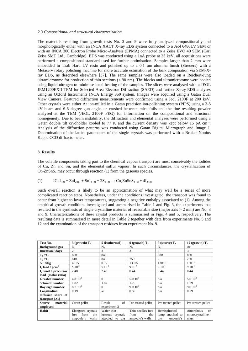
2.3 Compositional and structural characterization
The materials resulting from growth tests No. 3 and 9 were fully analyzed compositionally and
morphologically either with an INCA XACT X-ray EDS system connected to a Jeol 6480LV SEM or
with an INCA 300 Electron Probe Micro-Analysis (EPMA) connected to a Zeiss EVO 40 SEM (Carl
Zeiss SMT Ltd., Cambridge). EDS was conducted using a 1nA probe at 25 keV, all acquisitions were
performed a compositional standard used for further optimisation. Samples larger than 2 mm were
embedded in Taab Hard LV resin and polished up to a 0.1 μm alumina finish (Streuers) with a
Metaserv rotary polishing machine for more accurate estimation of the bulk composition via SEM-X-
ray EDS, as described elsewhere [37]. The same samples were also loaded on a Reichert-Jung
ultramicrotome for production of thin sections (< 90 nm). The blocks and ultramicrotome were cooled
using liquid nitrogen to minimise local heating of the samples. The slices were analysed with a JEOL
JEM1200EXII TEM for Selected Area Electron Diffraction (SAED) and further X-ray EDS analyses
using an Oxford Instruments INCA Energy 350 system. Images were acquired using a Gatan Dual
View Camera. Featured diffraction measurements were confirmed using a Jeol 2100F at 200 keV.
Other crystals were either Ar ion-milled in a Gatan precision ion-polishing system (PIPS) using a 3-5
kV beam and 6-8 degree gun angle, or crushed between mica foils and the fine resulting powder
analysed at the TEM (JEOL 2100F FEG) for information on the compositional and structural
homogeneity. Due to beam instability, the diffraction and elemental analyses were performed using a
Gatan double tilt cryoholder cooled to 77 K and the current density was kept below 15 pA·cm-1
.
Analysis of the diffraction patterns was conducted using Gatan Digital Micrograph and Image J.
Determination of the lattice parameters of the single crystals was performed with a Bruker Nonius
Kappa CCD diffractometer.
3. Results
The volatile components taking part to the chemical vapour transport are most conceivably the iodides
of Cu, Zn and Sn, and the elemental sulfur vapour. In such circumstances, the crystallization of
Cu2ZnSnS4 may occur through reaction (1) from the gaseous species.
(1) 2CuI (g) + ZnI2 (g) + SnI4 (g) + 2S2 (g) → Cu2ZnSnS4 (s) + 4I2 (g)
Such overall reaction is likely to be an approximation of what may well be a series of more
complicated reaction steps. Nonetheless, under the conditions investigated, the transport was found to
occur from higher to lower temperatures, suggesting a negative enthalpy associated to (1). Among the
empirical growth conditions investigated and summarised in Table 1 and Fig. 3, the experiments that
resulted in the synthesis of single crystalline material of reasonable size (major axis > 2 mm) are No. 3
and 9. Characterizations of these crystal products is summarised in Figs. 4 and 5, respectively. The
resulting data is summarised in more detail in Table 2 together with data from experiments No. 5 and
12 and the examination of the transport residues from experiment No. 9.
Test No. 3 (growth) T2 5 (isothermal) 9 (growth) T2 9 (source) T1 12 (growth) T2
Background gas N2 N2 N2 N2 Ar
Duration / days 2 3 3 3 3
T1 /°C 850 840 - 880 880
T2 /°C 810 840 750 - 750
ΔT /deg 40±5 0±5 130±5 130±5 130±5
I2 load / gcm-3 5∙10-3 5∙10-3 9∙10-4 9∙10-4 9∙10-4
I2 load / precursor
load (molar ratio)
2.48 2.48 0.44 0.44 0.44
Grashof number 4.8·104 0 5.0·103 n/a 5.0·103
Schmidt number 1.82 1.82 1.79 n/a 1.79
Rayleigh number 8.7·104 0 9.0·103 n/a 9.0·103
Longitudinal
diffusive share of
transport [23]
0.19 ∞ 0.59 n/a 0.59
Source material
employed
Green pellet Result of
experiment 3
Pre-treated pellet Pre-treated pellet Pre-treated pellet
Habit Elongated crystals
free from the ampoule’s walls
Wafer-thin
lustrous crystals attached to the
Thin needles free
from the ampoule’s walls
Hemispherical
lump attached to the ampoule’s
Amorphous or
microcrystalline mass

and edge-defined
crystals
ampoule’s walls walls
Mean size / mm 2-3 1-2 4 3 < 0.5
Composition
(SEM-EDS)
Cu2.0Zn1.0Sn1.0S4.0
Cu2.2Zn1.0Sn2.4S10.4
CuI, ZnS
n/a Cu1.9Zn0.9Sn1.0S4.1
CuI
Cu2.0Zn<0.1Sn1.0S3.0
CuS
CuI
n/a
Lattice parameters
(XRD)
a = b = 5.421(1) Ǻ c = 10.819(3) Ǻ
volume = 318 Ǻ3
α = β = γ = 90 ° c/(2a) = 0.998
n/a a = b = 5.4290(2) Å
c = 10.8340(4) Å
volume = 319 Ǻ3 α = β = γ = 90 °
c/(2a) = 0.998
n/a n/a
Lattice parameters
(SAED)
a = b= 5.55 Ǻ c = 10.52 Ǻ
volume = 324 Ǻ3
α = β = γ = 90 ° c/(2a) = 0.948
(at 77 K)
n/a a = b = 5.67 Å c = 11.48 Å
volume = 369 Ǻ3
α = β = γ = 90 ° c/(2a) = 1.012
(at 298 K)
n/a n/a
Relevant figures 3a, 4a-i 3b 3c, 5a-c,h-i 3d, 5d-g 3e
Relevant literature
of CZTS lattice
parameters from
different synthesis
routes (XRD)
CVT single crystal: a=b= 5.427, c=10.848, volume= 319 Ǻ3 Schäfer et al. [20] (1974)
CVT single crystal: a=b= 5.435, c=10.843, volume= 320 Ǻ3 Guen et al. [38] (1979)
Salt flux single crystal: a=b= 5.434(1), c=10.856(1), volume= 320 Ǻ3 Bonazzi et al. [39] (2003)
Powder sol. st. reaction: a=b= 5.428(2), c=10.864(4), volume= 320 Ǻ3 Schorr et al. [35] (2007)
Table 2. Summary of transport conditions and results for the most significant growth experiments (No.
3, 5, 9 and 12) and compositional/structural properties of the relevant materials obtained (n/a= not
applicable/analysed). The CZTS lattice parameters as from relevant XRD literature are also reported
for comparison. For computation of the fluid numbers, the reader is referred to Klosse’s work [23].
Fig. 3 Zoomed pictures of the materials resulting from the growth experiments listed in Table 2:
experiments No. 3 (a), 5 (b), 9 at T2 (c), 9 at T1 (d) and 12 (e).
3.1 Growth with iodine load of 5·10-3
gcm-3
Fig. 4 shows collections of images relative to this growth experiment (No. 3). Fig. 4a shows the visual
appearance of the ampoule at the end of the growth test. Fig. 4b shows the morphology of a typical
edge-defined grain crystal, a reasonably even 3D growth was obtained. Part of the crystal surface is
depicted in Fig. 4c, where the compositional variation is highlighted by the EDS mapping of the
emission lines of the relevant elements under a 20 keV electron beam (Kα1(Cu), Kα1(Zn), Lα1(Sn), Kα1(S),
Lα1(I)). The resulting picture shows the presence of three phases: a substrate phase consistent with the
composition Cu2ZnSnS4 (brown), covered by crystals of ZnS (orange) and CuI (blue).
In order to get more insights into the growth mechanism, some of the crystals were embedded in hard
resin and polished on random orientations as to examine the core morphology and composition. The
micro-scale compositional uniformity was assessed on the carbon coated specimens via Backscatter
Electron Composition imaging and EDS point analyses at the SEM. The cross sectional morphology of
the crystals shows that the bulk structure is rather defective with abundant voids of size up to 20 µm. A
CASINO V2.42 [40] simulation of the 20 keV electron beam trajectories in bulk Cu2ZnSnS4 was run in
order to estimate the interaction volume that defines the spatial resolution of the point EDS analyses
(Fig. 4d). The microprobe analyses performed this way on numerous points randomly distributed reveal
a standard deviation lower than 1 at. % for each element present. A pure cobalt standard was used for

the optimisation of the collection conditions. Evidence of the high compositional uniformity is given by
the back-scattered electron (BSE) micrograph shown in Fig. 4g which was taken deliberately at very
high contrast in order to enhance the compositional variation. The comparison with the secondary
electron image in Fig. 5f shows contrast attributable to polishing artefacts rather than elemental
inhomogeneity.
The nano-scale compositional uniformity was estimated via TEM-EDS on 90 nm thin slices of crystals
cleaved from the embedded samples. Morphological analysis at the TEM shows the presence of
domains with different contrast on the order of 20 nm; however, no appreciable compositional and
structural differences were revealed either by EDS or SAED. TEM-EDS analyses performed at room
temperature under beam currents higher than 25 pAcm-1
revealed compositions that were consistently
poorer of Sn and S in the ratio 1:2 compared to the SEM-EDS analyses. This is consistent with the
evolution of SnS(g) and S2(g) from Cu2ZnSnS4(s) in high vacuum [41] due to local heating by
overexposure to the high energy electron beam (120 keV). Due to this unavoidable reaction, only the
Cu:Zn compositional ratio can be considered as a reliable figure. Such ratio was found to be roughly
2:1. If the specimens were kept cool in a double-tilt filter at 77 K, no change in composition was
observed even after prolonged beam exposure and the SAED interrogation revealed a consistent
tetragonal structure throughout the samples.
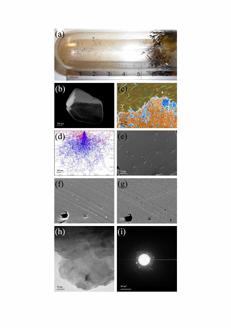
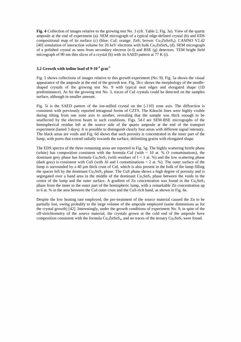
Fig. 4 Collection of images relative to the growing test No. 3 (cfr. Table 2, Fig. 3a). View of the quartz
ampoule at the end of experiment (a). SEM micrograph of a typical edge-defined crystal (b) and EDS
compositional map of its surface (c) (blue: CuI; orange: ZnS; brown: Cu2ZnSnS4). CASINO V2.42
[40] simulation of interaction volume for 20 keV electrons with bulk Cu2ZnSnS4 (d). SEM micrograph
of a polished crystal as seen from secondary electron (e-f) and BSE (g) detectors. TEM bright field
micrograph of 90 nm thin slices of a crystal (h) with its SAED pattern at 77 K (i).
3.2 Growth with iodine load of 9·10-4
gcm-3
Fig. 5 shows collections of images relative to this growth experiment (No. 9). Fig. 5a shows the visual
appearance of the ampoule at the end of the growth test. Fig. 5b-c shows the morphology of the needle-
shaped crystals of the growing test No. 9 with typical neat edges and elongated shape (1D
predominance). As for the growing test No. 3, traces of CuI crystals could be detected on the samples
surface, although in smaller amount.
Fig. 5i is the SAED pattern of the ion-milled crystal on the [-110] zone axis. The diffraction is
consistent with previously reported tetragonal forms of CZTS. The Kikuchi lines were highly visible
during tilting from one zone axis to another, revealing that the sample was thick enough to be
unaffected by the electron beam in such conditions. Figs. 5d-f are SEM-BSE micrographs of the
hemispherical residue left at the source side of the quartz ampoule at the end of the transport
experiment (lasted 3 days). It is possible to distinguish clearly four areas with different signal intensity.
The black areas are voids and Fig. 6d shows that such porosity is concentrated in the inner part of the
lump, with pores that extend radially towards the surface, delimiting grains with elongated shape.
The EDS spectra of the three remaining areas are reported in Fig. 5g. The highly scattering brittle phase
(white) has composition consistent with the formula CuI (with ~ 10 at. % O contaminations), the
dominant grey phase has formula Cu2SnS3 (with residues of I < 1 at. %) and the low scattering phase
(dark grey) is consistent with CuS (with Al and I contaminations < 2 at. %). The outer surface of the
lump is surrounded by a 40 µm thick crust of CuI, which is also present in the bulk of the lump filling
the spaces left by the dominant Cu2SnS3 phase. The CuS phase shows a high degree of porosity and is
segregated over a band area in the middle of the dominant Cu2SnS3 phase between the voids in the
centre of the lump and the outer surface. A gradient of Zn concentration was found in the Cu2SnS3
phase from the inner to the outer part of the hemispheric lump, with a remarkable Zn concentration up
to 6 at. % in the area between the CuI outer crust and the CuS-rich band, as shown in Fig. 6e.
Despite the low heating rate employed, the pre-treatment of the source material caused the Zn to be
partially lost, owing probably to the large volume of the ampoule employed (same dimensions as for
the crystal growth) [42]. Interestingly, under the growth conditions of experiment No. 9, in spite of the
off-stoichiometry of the source material, the crystals grown at the cold end of the ampoule have
composition consistent with the formula Cu2ZnSnS4, and no traces of the ternary Cu2SnS3 were found.

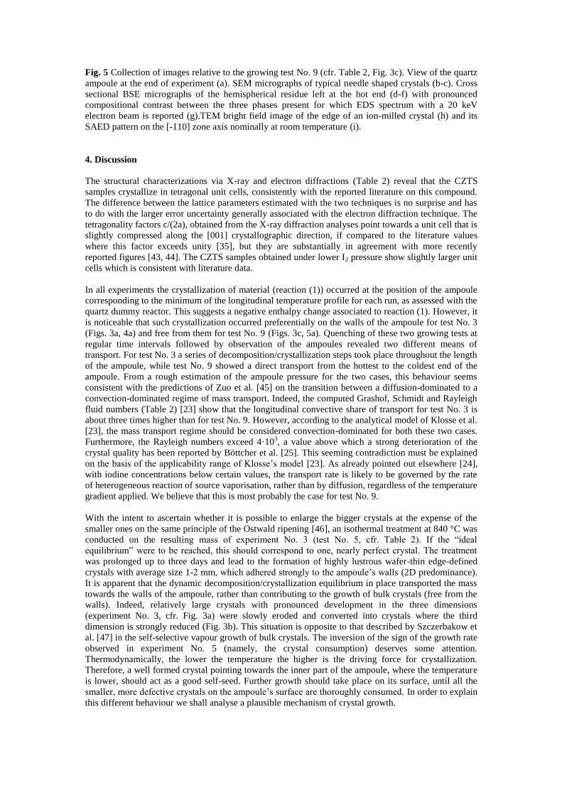
Fig. 5 Collection of images relative to the growing test No. 9 (cfr. Table 2, Fig. 3c). View of the quartz
ampoule at the end of experiment (a). SEM micrographs of typical needle shaped crystals (b-c). Cross
sectional BSE micrographs of the hemispherical residue left at the hot end (d-f) with pronounced
compositional contrast between the three phases present for which EDS spectrum with a 20 keV
electron beam is reported (g).TEM bright field image of the edge of an ion-milled crystal (h) and its
SAED pattern on the [-110] zone axis nominally at room temperature (i).
4. Discussion
The structural characterizations via X-ray and electron diffractions (Table 2) reveal that the CZTS
samples crystallize in tetragonal unit cells, consistently with the reported literature on this compound.
The difference between the lattice parameters estimated with the two techniques is no surprise and has
to do with the larger error uncertainty generally associated with the electron diffraction technique. The
tetragonality factors c/(2a), obtained from the X-ray diffraction analyses point towards a unit cell that is
slightly compressed along the [001] crystallographic direction, if compared to the literature values
where this factor exceeds unity [35], but they are substantially in agreement with more recently
reported figures [43, 44]. The CZTS samples obtained under lower I2 pressure show slightly larger unit
cells which is consistent with literature data.
In all experiments the crystallization of material (reaction (1)) occurred at the position of the ampoule
corresponding to the minimum of the longitudinal temperature profile for each run, as assessed with the
quartz dummy reactor. This suggests a negative enthalpy change associated to reaction (1). However, it
is noticeable that such crystallization occurred preferentially on the walls of the ampoule for test No. 3
(Figs. 3a, 4a) and free from them for test No. 9 (Figs. 3c, 5a). Quenching of these two growing tests at
regular time intervals followed by observation of the ampoules revealed two different means of
transport. For test No. 3 a series of decomposition/crystallization steps took place throughout the length
of the ampoule, while test No. 9 showed a direct transport from the hottest to the coldest end of the
ampoule. From a rough estimation of the ampoule pressure for the two cases, this behaviour seems
consistent with the predictions of Zuo et al. [45] on the transition between a diffusion-dominated to a
convection-dominated regime of mass transport. Indeed, the computed Grashof, Schmidt and Rayleigh
fluid numbers (Table 2) [23] show that the longitudinal convective share of transport for test No. 3 is
about three times higher than for test No. 9. However, according to the analytical model of Klosse et al.
[23], the mass transport regime should be considered convection-dominated for both these two cases.
Furthermore, the Rayleigh numbers exceed 4·103, a value above which a strong deterioration of the
crystal quality has been reported by Böttcher et al. [25]. This seeming contradiction must be explained
on the basis of the applicability range of Klosse’s model [23]. As already pointed out elsewhere [24],
with iodine concentrations below certain values, the transport rate is likely to be governed by the rate
of heterogeneous reaction of source vaporisation, rather than by diffusion, regardless of the temperature
gradient applied. We believe that this is most probably the case for test No. 9.
With the intent to ascertain whether it is possible to enlarge the bigger crystals at the expense of the
smaller ones on the same principle of the Ostwald ripening [46], an isothermal treatment at 840 °C was
conducted on the resulting mass of experiment No. 3 (test No. 5, cfr. Table 2). If the “ideal
equilibrium” were to be reached, this should correspond to one, nearly perfect crystal. The treatment
was prolonged up to three days and lead to the formation of highly lustrous wafer-thin edge-defined
crystals with average size 1-2 mm, which adhered strongly to the ampoule’s walls (2D predominance).
It is apparent that the dynamic decomposition/crystallization equilibrium in place transported the mass
towards the walls of the ampoule, rather than contributing to the growth of bulk crystals (free from the
walls). Indeed, relatively large crystals with pronounced development in the three dimensions
(experiment No. 3, cfr. Fig. 3a) were slowly eroded and converted into crystals where the third
dimension is strongly reduced (Fig. 3b). This situation is opposite to that described by Szczerbakow et
al. [47] in the self-selective vapour growth of bulk crystals. The inversion of the sign of the growth rate
observed in experiment No. 5 (namely, the crystal consumption) deserves some attention.
Thermodynamically, the lower the temperature the higher is the driving force for crystallization.
Therefore, a well formed crystal pointing towards the inner part of the ampoule, where the temperature
is lower, should act as a good self-seed. Further growth should take place on its surface, until all the
smaller, more defective crystals on the ampoule’s surface are thoroughly consumed. In order to explain
this different behaviour we shall analyse a plausible mechanism of crystal growth.

Fig. 6 shows a schematic representation of the consequences of CVT under longitudinally isothermal
conditions (e.g experiment No. 5, cfr. Table 2). The two scenarios with different directions of transport
are depicted in proximity of the ampoule’s walls respectively towards (a) and from (b) a well-
developed crystal. In general we can expect that the transversal profiles of temperature and thermal
conductivity across the media in the closed ampoule and the pressure of free transporting agent have an
effect on the thermodynamics (ΔG°) and kinetics (ΔG≠) of the crystallization reaction. As a first
approximation we can assume that reaction (1) proceeds via absorption of unary iodide molecules onto
the surface of the system, followed by collision with sulfur molecules (or vice versa), leading to the
release of iodine and the formation of a binary sulfide nucleus. Due to the entropy reduction,
spontaneous chemisorptions are associated to a negative enthalpy change. This means that colder
surfaces are thermodynamically more convenient for this step to take place. Furthermore, according to
the transition-state theory [48], the transition-state complex that forms when two molecules react has an
enthalpy greater than the sum of the enthalpy of the reagents or the sum of the enthalpy of the products.
Its high energy content makes the stability of the transition-state complex strongly affected by the local
temperature. Overall, both these hypothetic steps for the formation of binary sulfide nuclei are
exothermic and are therefore favoured by lower surface temperature. However, due to the exothermic
nature of the process, local temperature is bound to rise if heat is not effectively dissipated to the
surrounding. Reduction of the rate of crystal growth as growth proceeds is a known phenomenon. For
example, in conventional vapour growth methods like the Piper-Polich [49] and the Markov-Davydov
[50] this self-limiting behaviour is attributed to the fact that the growth front is located at the hottest
part of the crystal and is therefore bottle-necked by the heat transfer through the volume of the material
being grown (which is determined by its thermal conduction properties) [47].
When RT > ΔG≠ and under longitudinally isothermal conditions, a dynamic equilibrium tend to be
established, where the rate of crystallization equals the rate of decomposition. If the heat flux away
from the crystal is lower than the flux directed towards its surface arising from crystallization, the local
temperature will rise until it exceeds the temperature of the ampoule’s walls, at which point the
direction of transport is inverted. Under these circumstances, if the thermal conductivity of the material
being grown is lower than that of the ampoule’s walls the crystal is inherently unstable and bound to
fully deplete at the time when the dynamic equilibrium is reached. A net material transport occurs from
the crystals free from the walls to the ampoule’s walls.
In steady state conditions, the decomposition/crystallization rate is ultimately dependent on the
concentrations of free I2 and S2 in the system. Higher iodine loads correspond to higher
decomposition/crystallization rates of CZTS. Since heat is released in the vicinity of the process when
reaction (1) is taking place, more heat needs to be exchanged per time unit if higher iodine loads are
employed. Depending on the relative resistance to heat transfer of the material being grown and the
vessel, as a consequence of the local temperature variation induced by the reaction, the activation free
energy for process (a) will be more or less affected than (b) by the concentration of free I2 in the
ampoule. In general, there will be a limiting iodine pressure corresponding to a steady state
decomposition/crystallization rate for which the local temperature of the crystal free from the walls
equals the temperature of the ampoule’s walls. We call this limiting pressure # (Fig. 6). For pressures
higher than # crystallization shall occur on the surface of the ampoule’s walls (Fig. 6b), while pressures
lower than # shall give rise to crystal enlargement (Fig. 6a).

Fig. 6 Chemical vapour transport scenarios (a-b) during longitudinally isothermal treatment (e.g. test
No. 5 cfr. Table 2, Fig. 3b). The figure depicts the geometry of the experiment in proximity of the
ampoule’s walls with transversal profiles of temperature and thermal conductivity (in this example the
thermal conductivity of the material being grown is chosen lower than that of the quartz ampoule). The
experimental observation for the two different transport phenomena is summarised by the simplistic
free energy paths reported. If the pressure of free transporting agent exceeds a limiting value #,
crystallization via path (b) prevails on (a) and vice versa.

In our experimental setup the transversal profile of thermal conductivity is such that a more efficient
heat extraction can be attained by the ampoule’s walls rather than by large crystals surrounded by the
complex mixture of reacting gases (Fig. 6). For experiment No. 5, carried out at 840 °C with an iodine
load of 5·10-3
gcm-3
, this is translated into a faster kinetics for crystallization on the ampoule’s walls
(Fig. 6b) rather than on the surface of already formed crystals (Fig. 6a), despite the expected lower bulk
temperature of such crystals.
This proposed mechanism gives also a plausible explanation as to why bulk CZTS crystals free from
the walls were obtained at all during experiment No. 3. Such crystals were formed before the steady
state equilibrium was reached, i.e. when part of the I2 was sequestered by the material to be transported
from the higher temperature end of the ampoule, giving rise to a lower effective
decomposition/crystallization rate. Similarly, it is explained why with lower initial I2 loads (test No. 9,
cfr. Table 2, Figs. 3c, 5a) the crystallization occurred preferentially free from the ampoule’s walls
rather than at their surface. Experiment No. 12 (cfr. Table 2, Fig. 3e) was run under the same
conditions of experiment No. 3 but using Ar instead of N2 as the background gas. This choice lead to
the formation of an amorphous or microcrystalline mass, consistently with a lower thermal
conductivity of the atmosphere inside the ampoule [51].
At the end of the experiment performed with lower I2 load (No. 9), the mass transport was found
incomplete. EDS microstructure analyses were performed on the residues of the source material (sect.
3.2) in order to gain information on the mechanism of CVT (Fig. 5d-g). The interpretation that can be
drawn is as follows. Under the growth conditions (T1 = 880 °C) the Zn poor CZTS precursor is mainly
liquid (m.p. Cu2SnS3 ~ 837 °C [52]). This allows the Zn atoms (limiting reagent) to diffuse easily
through the droplet towards the surface where they are captured by the I2 (g) to form ZnI2 (g). The other
metals also react with iodine and the formation of nearly stoichiometric CZTS at the cold end
withdraws the mixture of gaseous iodides until there is enough Zn to be extracted from the source. The
CuI formed by reaction of the CZTS precursor with I2 is liquid at the test temperature (m.p. = 605 °C
[52]). During cooling, the matrix of Cu2SnS3 crystallizes in elongated grains, the molten CuI remains
trapped at the grain boundaries and the shrinkage due to its solidification causes this phase to be
surrounded by voids. The Zn concentration gradient left over in the source material is opposite to what
it would be expected if Zn were to be selectively leached. Indeed, due to the heterogeneous reaction
occurring at the interface between gaseous I2 and condensed source material, such phenomenon would
likely lead to a Zn poor surface and a Zn rich core. There appears to be no obvious explanations for
such observation. No traces of ZnI2 (b.p = 726 °C), SnI4 (b.p = 353 °C) and SnI2 (b.p = 717 °C) were
found in the solid residue of the source material, as their boiling points are lower than the solidification
temperature of Cu2SnS3. The fact that these iodides are not detected at the cold end too, suggests that
their stabilities is lower (higher reactivity) compared to that of CuI. Despite the Zn deficiency of the
source material, no Cu2SnS3 was found at the cold end of the ampoule. This suggests that, to a
reasonable extent, the system shows the tendency to self-adjust the crystal growth as to produce the
most stable phase (in this case Cu2ZnSnS4) so long as sufficient amounts of each component (e.g. Zn)
are available at the source end. Indeed, comparison of the EDS analyses of the main (CZTS) sinks for
experiments No. 3 and 9 reveal that the composition is nearly unaffected by the I2 pressure within the
ampoules (cfr. Table 2), although increased amounts of secondary phases were detected when the
larger I2 load was employed.
5. Conclusion
High quality single crystals of Cu2ZnSnS4 solar absorber materials have been synthesized from the
elements via the Chemical Vapour Transport in the presence of I2. In agreement with simpler systems,
it was found that an increase of the initial iodine load has a strong effect on the transport mechanism,
with a transition from a diffusion (reaction-limited) to a convection-dominated regime [25]. In turn,
this was found to affect significantly the shape and quality of the crystals. Highly crystalline CZTS
with needle-shape (1D predominance) was obtained with 9·10-4
gcm-3
of I2, while more defective but
larger crystals (3D predominance) were obtained with a nearly five-fold load. In the first case a
gradient of 130 °C was employed to speed up the process and achieve well-formed crystals, while in
the second case a gradient of 40 °C was necessary as larger gradients lead to the formation of
polycrystalline material. There appears to be no meaningful effect of the iodine pressure employed on
the composition of the CZTS samples. However, XRD analysis shows that samples obtained under
lower I2 pressure have slightly larger unit cells. Neutron diffraction and Raman spectroscopy analyses
would be required in order to ascertain if the crystals obtained under different pressure conditions have
significant structural differences. These two techniques are crucial, due to the great complexity of the
phase identification for the Cu-Zn-Sn-S system solely by XRD [41, 43, 53, 54].
The samples showed high compositional uniformity at the SEM/EDS/BSE level. The nanoscale
compositional uniformity may be better investigated with more sophisticated transmission electron
techniques. These would also add important information on the defect nature of the samples.
New CVT treatments in the absence of longitudinal temperature gradients were carried out with the
aim of increasing the size of already formed crystals. Under the investigated conditions, the nucleation
and growth of CZTS on the ampoule’s walls (2D predominance) was kinetically more convenient than
the enlargement of pre-existing CZTS crystals pointing towards the interior of the ampoule (3D
predominance). A schematic crystallization reaction mechanism is proposed to account for the
experimental observations. Under longitudinally isothermal CVT, based on our argument we can
conclude as follows.
With high transporting agent loads the position on the system’s surface corresponding to the most
effective path for heat extraction is likely to show the fastest crystallization kinetics, because self-
inhibition occurs elsewhere due to local temperature variation (induced by the enthalpy of reaction).
Under lower transporting agent pressures (i.e. with lower decomposition/crystallization rates) local
temperature variation is negligible and the direction of crystallization dictated by the sign of the
enthalpy of compound transport follows the naturally occurring transversal profile of temperature
within the system.
More studies are required in order to confirm our hypothesis and establish the conditions for which
CZTS crystal enlargement/improvement via chemical vapour transport in isothermal treatments can be
made feasible. The influence of ampoules made of more insulating materials or, vice versa, the increase
of the thermal conductivity of the atmosphere within the ampoule, might help making this process
kinetically viable. Alternatively, formation of large CZTS crystals may be possible by a two stage CVT
process where crystals free from the walls are first produced under high iodine loads with longitudinal
temperature gradient quenched before the attainment of the steady state equilibrium, followed by a
second longitudinally isothermal treatment performed with a lower iodine load. It is hoped that this
new CVT approach will encounter the interest of the crystal growers’ community.
An estimation of the temperature at which the crystal growth reaction of CZTS becomes
thermodynamically spontaneous would be beneficial for the design of the growth experiments. In
future, thermochemical and computational investigations could give important additional information.
Acknowledgements
Phil Jones is gratefully acknowledged for providing the quartz/glass joints and for his glassblowing
experience required for sealing off the ampoules. Funding was provided by EPSRC (Supergen:
Photovoltaic Materials for the 21st Century EP/F029624/1).
References
[1] H. Katagiri, N. Sasaguchi, S. Hando, S. Hoshino, J. Ohashi, T. Yokota, Preparation and evaluation
of Cu2ZnSnS4 thin films by sulfurization of E---B evaporated precursors, Solar Energy Materials and
Solar Cells, 49 (1997) 407-414.
[2] T.K. Todorov, K.B. Reuter, D.B. Mitzi, High-Efficiency Solar Cell with Earth-Abundant Liquid-
Processed Absorber, Advanced Materials, 22 (2010) E156-E159.
[3] D.A.R. Barkhouse, O. Gunawan, T. Gokmen, T.K. Todorov, D.B. Mitzi, Device characteristics of a
10.1% hydrazine-processed Cu2ZnSn(Se,S)4 solar cell, Progress in Photovoltaics: Research and
Applications, 20 (2012) 6-11.
[4] B.A. Andersson, Materials availability for large-scale thin-film photovoltaics, Progress in
Photovoltaics: Research and Applications, 8 (2000) 61-76.

[5] L.M. Peter, P.J. Dale, J.J. Scragg, G. Zoppi, I. Forbes, New routes to sustainable photovoltaics:
evaluation of Cu2ZnSnS4 as an alternative absorber material, Physica Status Solidi (b), 245 (2008)
1772-1778.
[6] C. Wadia, A.P. Alivisatos, D.M. Kammen, Materials Availability Expands the Opportunity for
Large-Scale Photovoltaics Deployment, Environmental Science & Technology, 43 (2009) 2072-2077.
[7] K. Tanaka, Y. Miyamoto, H. Uchiki, K. Nakazawa, H. Araki, Donor-acceptor pair recombination
luminescence from Cu2ZnSnS4 bulk single crystals, physica status solidi (a), 203 (2006) 2891-2896.
[8] K. Muska, M. Kauk, M. Altosaar, M. Pilvet, M. Grossberg, O. Volobujeva, Synthesis of Cu2ZnSnS4
monograin powders with different compositions, Energy Procedia, (2011).
[9] I.D. Olekseyuk, I.V. Dudchak, L.V. Piskach, Phase equilibria in the Cu2S-ZnS-SnS2 system,
Journal of Alloys and Compounds, 368 (2004) 135-143.
[10] T. Shimada, K. Oishi, K. Jimbo, H. Katagiri, H. Araki, O. Yoshida, M. Yamazaki, S. Kobayashi,
N. Tsuboi, Crystal growth of Cu2ZnSnS4 by melting method, in: IEICE Technical report, 2005.
[11] M. Lachab, A.A. Attia, C. Llinarès, Study on the properties of CuInSe2 ingots grown from the
melt using stoichiometric and non-stoichiometric charges, Journal of Crystal Growth, 280 (2005) 474-
482.
[12] H. Matsushita, T. Ichikawa, A. Katsui, Structural, thermodynamical and optical properties of Cu2-
II-IV-VI4 quaternary compounds, Journal of Materials Science, 40 (2005) 2003-2005.
[13] G.P. Bernardini, P. Bonazzi, M. Corazza, F. Corsini, G. Mazzetti, L. Poggi, G. Tanelli, New data
on the Cu2FeSnS4-Cu2ZnSnS4 pseudobinary system at 750°C and 550°C, European Journal of
Minerals, 2 (1990) 219-225.
[14] G.H. Moh, L.A. Taylor, Laboratory techniques in experimental sulfide petrology, Neues Jahrbuch
für Mineralogie - Monatshefte, (1971) 450-459.
[15] M. Altosaar, J. Raudoja, K. Timmo, M. Danilson, M. Grossberg, J. Krustok, E. Mellikov, Cu2Zn1-x
Cdx Sn(Se1-y Sy)4 solid solutions as absorber materials for solar cells, Physica Status Solidi (a), 205
(2008) 167-170.
[16] K. Timmo, M. Altosaar, J. Raudoja, K. Muska, M. Pilvet, M. Kauk, T. Varema, M. Danilson, O.
Volobujeva, E. Mellikov, Sulfur-containing Cu2ZnSnSe4 monograin powders for solar cells, Solar
Energy Materials and Solar Cells, 94 (2010) 1889-1892.
[17] M. Altosaar, A. Jagomägi, M. Kauk, M. Krunks, J. Krustok, E. Mellikov, J. Raudoja, T. Varema,
Monograin layer solar cells, Thin Solid Films, 431-432 (2003) 466-469.
[18] A. Nagaoka, K. Yoshino, H. Taniguchi, T. Taniyama, H. Miyake, Preparation of Cu2ZnSnS4
single crystals from Sn solutions, Journal of Crystal Growth, (2012).
[19] R. Nitsche, D.F. Sargent, P. Wild, Crystal growth of quaternary 122464 chalcogenides by iodine
vapour transport, Journal of Crystal Growth, 1 (1966).
[20] W. Schäfer, R. Nitsche, Tetrahedral quaternary chalcogenides of the type Cu2-II-IV-S4(Se4),
Materials Research Bulletin, 9 (1974).
[21] S. Levcenko, V.E. Tezlevan, E. Arushanov, S. Schorr, T. Unold, Free-to-bound recombination in
near stoichiometric Cu2ZnSnS4 single crystals, Physical Review B, 86 (2012) 045206.
[22] K. Klosse, A new productivity function and stability criterion in chemical vapor transport
processes, Journal of Solid State Chemistry, 15 (1975) 105-116.
[23] K. Klosse, P. Ullersma, Convection in a chemical vapor transport process, Journal of Crystal
Growth, 18 (1973) 167-174.
[24] K. Böttcher, H. Hartmann, Zinc selenide single crystal growth by chemical transport reactions,
Journal of Crystal Growth, 146 (1995) 53-58.
[25] K. Böttcher, H. Hartmann, R. Röstel, Influence of convection on zinc selenide single crystal
growth by chemical vapour transport, Journal of Crystal Growth, 159 (1996) 161-166.
[26] K. Böttcher, H. Hartmann, D. Siche, Computational study on the CVT of the ZnSe–I2 material
system, Journal of Crystal Growth, 224 (2001) 195-203.
[27] D. Siche, K. Böttcher, U. Rinas, H. Hartmann, Crystal growth of zinc selenide under μg-
conditions, Journal of Crystal Growth, 244 (2002) 249-256.
[28] M.M. Faktor, I. Garrett, Growth of crystals from the vapour, Chapman and Hall, Ltd., London,
1976.
[29] R. Gruehn, R. Glaum, New Results of Chemical Transport as a Method for the Preparation and
Thermochemical Investigation of Solids, Angewandte Chemie International Edition, 39 (2000) 692-
716.
[30] M. Lenz, R. Gruehn, Developments in Measuring and Calculating Chemical Vapor Transport
Phenomena Demonstrated on Cr, Mo, W, and Their Compounds, Chemical Reviews, 97 (1997) 2967-
2994.

[31] B.I. Noläng, M.W. Richardson, The transport flux function - A new method for predicting the rate
of chemical transport in closed systems: I. Theory, Journal of Crystal Growth, 34 (1976) 198-204.
[32] H. Schäfer, Chemical Transport Reactions, Academic Press Inc., 1964.
[33] I. Jandl, K.W. Richter, H. Ipser, Incongruent, time-dependent chemical vapour transport in multi-
component systems: A case study in Cr-Ge-Si, Solid State Sciences, 13 (2011) 1108-1114.
[34] P. Prabukanthan, R. Dhanasekaran, Stoichiometric single crystal growth of AgGaS2 by iodine
transport method and characterization, Crystal Research and Technology, 43 (2008) 1292-1296.
[35] S. Schorr, H.-J. Hoebler, M. Tovar, A neutron diffraction study of the Stannite-Kesterite solid
solution series, European Journal of Minerals, 19 (2007).
[36] K. Hönes, E. Zscherpel, J. Scragg, S. Siebentritt, Shallow defects in Cu2ZnSnS4, Physica B:
Condensed Matter, 404 (2009) 4949-4952.
[37] S. Delsante, R. Raggio, G. Borzone, Phase relations of the Sm–Ni–Al ternary system at 500°C in
the 40–100 at.% Al region, Intermetallics, 16 (2008) 1250-1257.
[38] L. Guen, W.S. Glaunsinger, A. Wold, Physical properties of the quarternary chalcogenides
Cu2IBIICIVX4 (BII = Zn, Mn, Fe, Co; CIV = Si, Ge, Sn; X = S, Se), Materials Research Bulletin, 14
(1979) 463-467.
[39] P. Bonazzi, L. Bindi, G.P. Bernardino, S. Menchetti, A model for the mechanism of incorporation
of Cu Fe and Zn in the Stannite-Kesterite series Cu2FeSnS4-Cu2ZnSnS4, Canadian Mineralogist, 41
(2003).
[40] D. Drouin, A.R. Couture, D. Joly, X. Tastet, V. Aimez, R. Gauvin, CASINO V2.42 - A Fast and
Easy-to-use Modeling Tool for Scanning Electron Microscopy and Microanalysis Users, Scanning, 29
(2007) 92-101.
[41] A. Weber, R. Mainz, H.W. Schock, On the Sn loss from thin films of the material system Cu--Zn--
Sn--S in high vacuum, Journal of Applied Physics, 107 (2010) 013516-013516.
[42] A. Klimova, V. Ananichev, M. Arif, L. Blinov, Investigation of the Saturated Vapor Pressure of
Zinc, Selenium, and Zinc Selenide, Glass Physics and Chemistry, 31 (2005) 760-762.
[43] S. Schorr, The crystal structure of kesterite type compounds: A neutron and X-ray diffraction
study, Solar Energy Materials and Solar Cells, 95 (2011) 1482-1488.
[44] S. Schorr, G. Gonzalez-Aviles, In-situ investigation of the structural phase transitions in Kesterite,
Phys. Status Solidi A, 206 (2009).
[45] R. Zuo, W. Wang, Theoretical study on chemical vapor transport of ZnS-I2 system. Part II:
numerical modeling, Journal of Crystal Growth, 236 (2002) 695-710.
[46] F.W. Ostwald, Lehrbuch der Allgemeinen Chemie, Engelmann, Leipzig, 1896.
[47] A. Szczerbakow, K. Durose, Self-selecting vapour growth of bulk crystals : Principles and
applicability, Progress in Crystal Growth and Characterization of Materials, 51 (2005) 28.
[48] H. Eyring, The Activated Complex in Chemical Reactions, The Journal of Chemical Physics, 3
(1935) 107-115.
[49] W.W. Piper, S.J. Polich, Vapor-Phase Growth of Single Crystals of II--VI Compounds, Journal of
Applied Physics, 32 (1961) 1278-1279.
[50] E.V. Markov, A.A. Davydov, Izvestiya Akademii Nauk SSSR - Neorganicheskie Materialy, 7
(1971) 575.
[51] Handbook of Chemistry and Physics, 89th
ed., CRC/Taylor and Francis, Boca Raton, 2009.
[52] L.I. Berger, B.R. Pamplin, Properties of semiconductors - Handbook of Chemistry and Physics,
89th
ed., CRC/Taylor and Francis, Boca Raton, 2009.
[53] X. Fontané, L. Calvo-Barrio, V. Izquierdo-Roca, E. Saucedo, A. Perez-Rodriguez, J.R. Morante,
D.M. Berg, P.J. Dale, S. Siebentritt, In-depth resolved Raman scattering analysis for the identification
of secondary phases: Characterization of Cu2ZnSnS4 layers for solar cell applications, Applied Physics
Letters, 98 (2011) 181905-181903.
[54] P.A. Fernandes, P.M.P. Salomé, A.F. da Cunha, Growth and Raman scattering characterization of
Cu2ZnSnS4 thin films, Thin Solid Films, 517 (2009) 2519-2523.