courtesy of s. salahuddin (uc berkeley) lecture 4ee290d/fa13/lecturenotes/lecture4.pdf · (cs) d....
TRANSCRIPT

Lecture 4• MOSFET Transport Issues
– semiconductor band structure– quantum confinement effects– low-field mobility and high-field saturation
Reading: - M. Lundstrom, “Fundamentals of Carrier Transport,” 2nd edition,
Cambridge University Press, 2000.- multiple research articles (reference list at the end of this lecture)
9/23/2013 1Nuo Xu EE 290D, Fall 2013
Courtesy of S. Salahuddin (UC Berkeley)
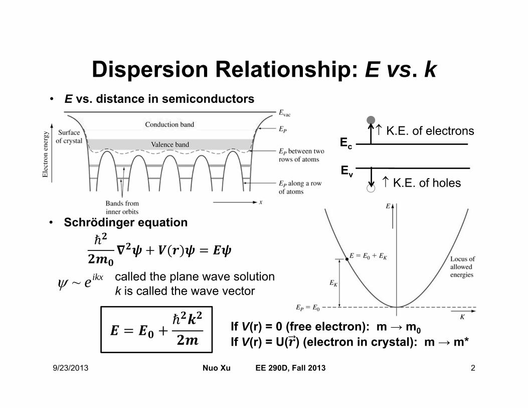
Dispersion Relationship: E vs. k
~ eikx called the plane wave solutionk is called the wave vector
Ec
Ev
K.E. of electrons
K.E. of holes
9/23/2013 2Nuo Xu EE 290D, Fall 2013
• E vs. distance in semiconductors
• Schrödinger equation
If V(r) = 0 (free electron): m → m0If V(r) = U( ) (electron in crystal): m → m*

Semiconductor Band Structure
L L
43210-1-2-3-4
GaAs Si
Ener
gy (e
V)
9/23/2013 3Nuo Xu EE 290D, Fall 2013
Zinc-blende structure
• E vs. k
• Reciprocal space Fourier Transform as

Silicon Band Structure• Equi-energy contours
Electrons HolesHeavy Hole
Light Hole
Split-off
• E-k relationship is direction-dependent for electrons in solids.• In Si, electrons have a more parabolic E-k relationship than holes.
9/23/2013 4Nuo Xu EE 290D, Fall 2013
Valley degeneracy: 2Spin degeneracy: 2
Valley degeneracy: 1Spin degeneracy: 2
T. Guillaume, SSE (2006)
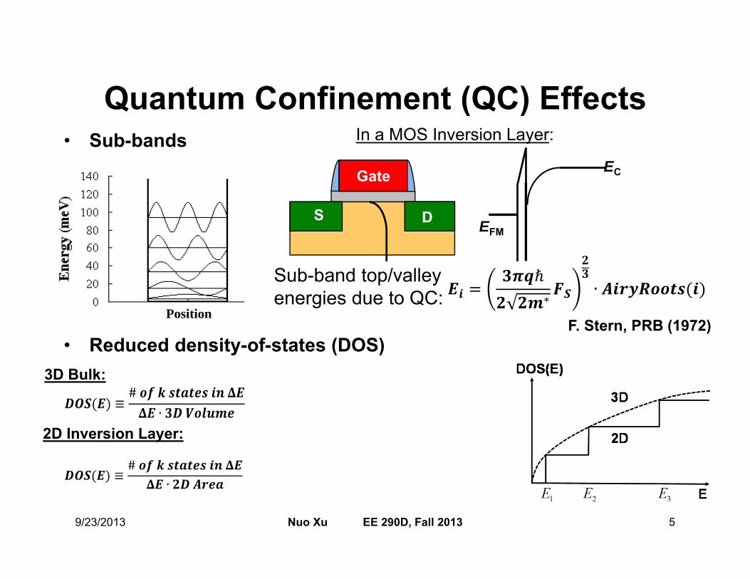
Quantum Confinement (QC) Effects• Sub-bands
• Reduced density-of-states (DOS)
In a MOS Inversion Layer:
Position
9/23/2013 5Nuo Xu EE 290D, Fall 2013
Sub-band top/valley energies due to QC:
F. Stern, PRB (1972)
3D Bulk:
2D Inversion Layer:
Gate
S D EFM
EC

QC Effect on Si Band Structure: Electrons
9/23/2013 6Nuo Xu EE 290D, Fall 2013
0 5 10 15 20 25
0.00
0.05
0.10
0.15
0.20
"Bulk" EC
4, 1st
2, 2nd
2, 1st
Di t fDepth from oxide/Si interface (nm)
Electron Sub-band Energies
(100) Si Ns=2×1012 cm-2
∆
∆Valley degeneracy:
Δ2: 2 Δ4: 4Spin degeneracy: 2Δk
E+ΔEE

QC Effect on Si Band Structure: Holes
9/23/2013 7Nuo Xu EE 290D, Fall 2013
kz=0
N. Xu, Ph.D. thesis (2012)
QC
0 5 10 15 20 25-0.20
-0.15
-0.10
-0.05
0.00
0.05
LH-SO, 1st
"Bulk" EV
HH, 2nd
HH, 1st
Depth from oxide/Si interface (nm)
Hole Sub-band Energies
(100) Si Ns=2×1012 cm-2
Valley degeneracy: HH: 1 LH-SO: 2
Spin degeneracy: 2

CTinv
Impacts of QC on MOS Electrostatics
9/23/2013 8Nuo Xu EE 290D, Fall 2013
• Inversion Thickness (Tinv)
• Quantum Capacitance
Measured Tinv in Si Bulk CMOSFETs
K. Yang, VLSI-T (1999)Cox
Cdep
Cox
Cdep
CTinv
Cox
Cdep
Cox
Cinv Cdep Cinv
Classic QM
OFF
ON
Physical Oxide Thickness (tox) Effective Oxide Thickness (EOT) Electrical Effective Oxide
Thickness (EOTelec)
Hence there are 3 metrics to characterize Cgate …
0 5 10 150
1
2
3
4
5
6
7
0 5 10 15Distance from Top SiO2/Si Interface (nm)
Inve
rsio
n H
ole
Con
cent
ratio
n (a
.u.)
Increasing gate voltage

Carrier Mobility: A Quantum Mechanical View
2*
, ' '( ) ( )n n n nz
F dz z z
, ,2 2
1 ( ) (1 ( ))(2 )i j
n nn n ni j n n
B n i jk
e g dk E E f E f Ek T n k k
, ,
1i j i j
tot nn
ntot
nn
' '
' ' '',
2 ( , , , ) ( ( ) ( ) )n nnk n kS M n k n k E k E k
9/23/2013 9Nuo Xu EE 290D, Fall 2013
• Fermi Golden Rule
• mobility
for the nth sub-band
for the overall inversion layer
E
k(n,k)
(n’,k’)
' '
'' '
2 ,'
1 ( , )(2 )( ) nk n k
nn k
d k S nk n kk
scattering rates for sub-band n at k
(n,k)
sub-b 1 sub-b n’… …wavefuntion overlap along confinement direction
: transition rates between two quantum states
: scattering-induced quantum state transitions
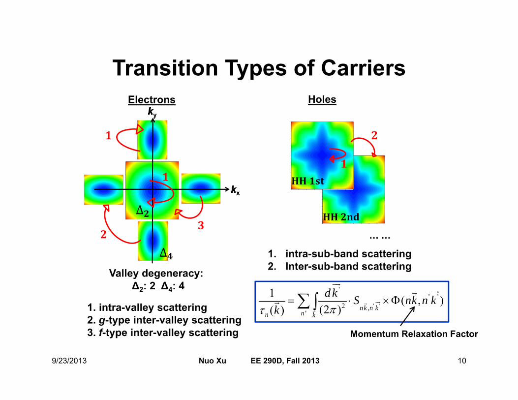
Transition Types of Carriers
9/23/2013 10Nuo Xu EE 290D, Fall 2013
∆
∆Valley degeneracy:
Δ2: 2 Δ4: 4
Electrons Holes
1. intra-valley scattering2. g-type inter-valley scattering3. f-type inter-valley scattering
1. intra-sub-band scattering2. Inter-sub-band scattering
……
' '
'' '
2 ,'
1 ( , )(2 )( ) nk n k
nn k
d k S nk n kk
Momentum Relaxation Factor
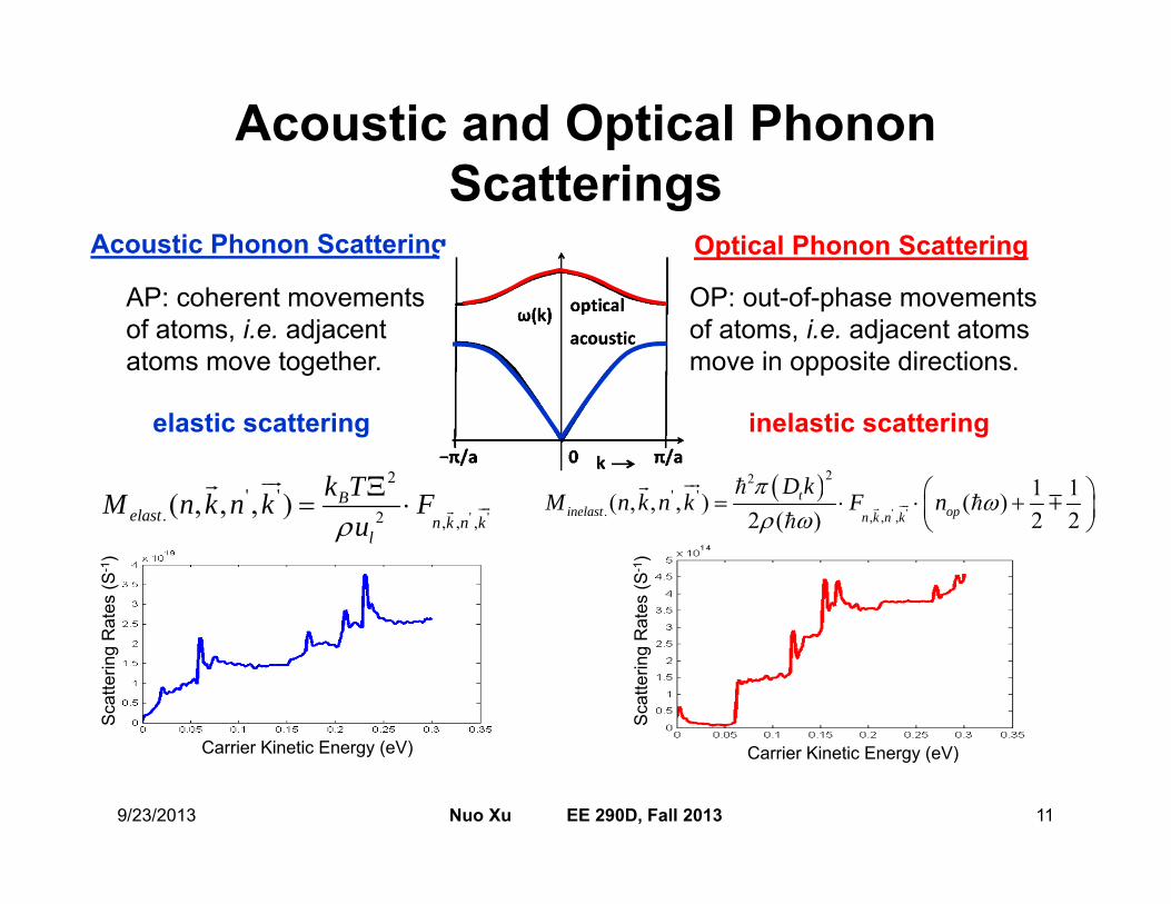
Acoustic and Optical Phonon Scatterings
' '
2' '
. 2 , , ,( , , , ) B
elast n k n kl
k TM n k n k Fu
' '
22' '
. , , ,
1 1( , , , ) ( )2 ( ) 2 2
tinelast opn k n k
D kM n k n k F n
9/23/2013 11Nuo Xu EE 290D, Fall 2013
Acoustic Phonon Scattering Optical Phonon Scattering
Sca
tterin
g R
ates
(S-1
)
Sca
tterin
g R
ates
(S-1
)
Carrier Kinetic Energy (eV) Carrier Kinetic Energy (eV)
elastic scattering inelastic scattering
AP: coherent movements of atoms, i.e. adjacent atoms move together.
OP: out-of-phase movements of atoms, i.e. adjacent atoms move in opposite directions.
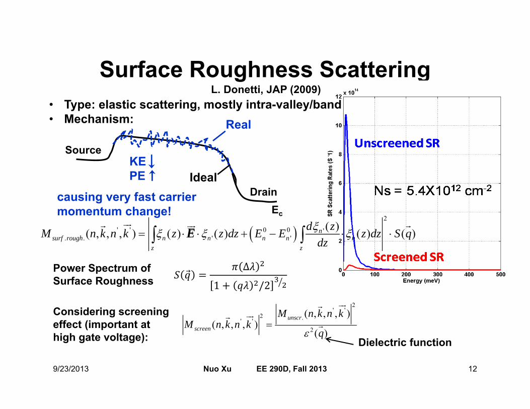
Surface Roughness Scattering
2' '
2 .' '2
( , , , )( , , , )
( )unscr
screen
M n k n kM n k n k
q
9/23/2013 12Nuo Xu EE 290D, Fall 2013
Considering screening effect (important at high gate voltage): Dielectric function
Power Spectrum of Surface Roughness
Source
DrainEc
KEPE Ideal
Real
2
' ' 0 0 '. . ' '
( )( , , , ) ( ) ( ) ( ) ( )nsurf rough n n n n n
z z
d zM n k n k z F z dz E E z dz S qdz
E
causing very fast carrier momentum change!
L. Donetti, JAP (2009)• Type: elastic scattering, mostly intra-valley/band• Mechanism:
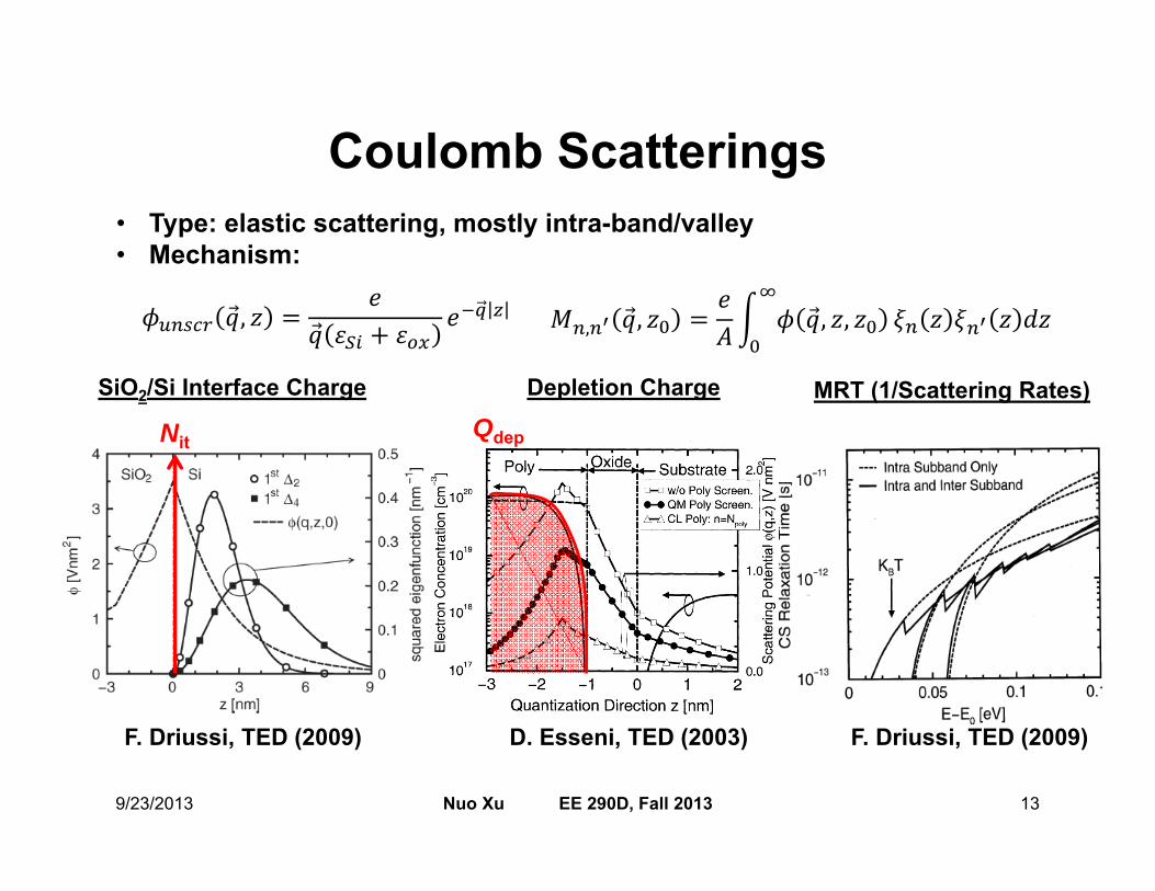
Coulomb Scatterings
9/23/2013 13Nuo Xu EE 290D, Fall 2013
• Type: elastic scattering, mostly intra-band/valley• Mechanism:
Nit
F. Driussi, TED (2009)
SiO2/Si Interface Charge
D. Esseni, TED (2003)
Depletion Charge
Qdep
MRT (1/Scattering Rates)
F. Driussi, TED (2009)

Effective Transverse Field (Eeff)
9/23/2013 14Nuo Xu EE 290D, Fall 2013
≡
Gate
S D
ECDepth
In a MOS Inversion Layer:
Surface (oxide/Si interface) field:
Bottom (of inversion layer) field:
Average field:
Xdep
E
∙More generally: For (100) bulk Si MOSFET:
Electrons: α = 0.5Holes: α = 0.33
2D Sheet Charge Density:
Depletion Approximation
Reality

Universal Mobility Curve: vs. Eeff
9/23/2013 15Nuo Xu EE 290D, Fall 2013
S. Takagi, TED (1994)
- enhanced screening effect
- Increased DOS effect
- Increased SR scattering
• Unify the electric field value by including the oxide thickness (compared to vs. VG) and depletion charge effect (compared to vs. Ninv).
Measured Si Universal Curves

Universal Mobility Curve: Dependent Factors
Y. Zhao, IEDM (2008)
O. Weber, VLSI-T (2007)
9/23/2013 16Nuo Xu EE 290D, Fall 2013
Temperature Band Structure
• Si universal mobility curves are often used to show a new technology’s enhancement.

Gate
S D
High--induced Scatterings
R. Chau, EDL (2004)
9/23/2013 17Nuo Xu EE 290D, Fall 2013
• Remote Coulomb Scattering
• Remote (Surface Optical) Phonon Scatterings
-(tSiO2+tHK) -tSiO2 0
Metal high-κ SiO2 SiGate
Nit
Coupled ModesHκ Modes
SiO2 Modes
Si Modes(AP, OP)
SiO2 ILHigh-κ
Courtesy of D. Vesileska (ASU)
C.-Y. Lu, EDL (2006)
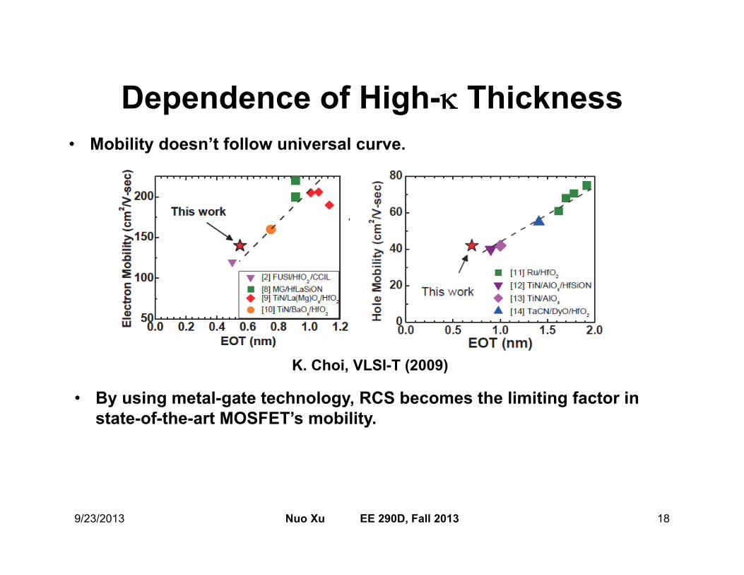
Dependence of High- Thickness
9/23/2013 18Nuo Xu EE 290D, Fall 2013
K. Choi, VLSI-T (2009)
• Mobility doesn’t follow universal curve.
• By using metal-gate technology, RCS becomes the limiting factor in state-of-the-art MOSFET’s mobility.
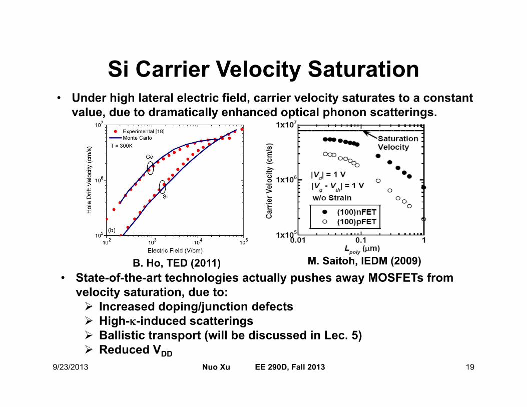
Si Carrier Velocity Saturation
M. Saitoh, IEDM (2009)
9/23/2013 19Nuo Xu EE 290D, Fall 2013
B. Ho, TED (2011)
• Under high lateral electric field, carrier velocity saturates to a constant value, due to dramatically enhanced optical phonon scatterings.
• State-of-the-art technologies actually pushes away MOSFETs from velocity saturation, due to: Increased doping/junction defects High--induced scatterings Ballistic transport (will be discussed in Lec. 5) Reduced VDD

ReferencesBand Structure1. T. Guillaume, M. Mouis, “Calculations of Hole Mass in [110]-Uniaxially Strained Silicon for the Stress
Engineering of p-MOS Transistors,” Solid-State Electronics, Vol. 50, pp. 701-708, 2006.2. N. Xu, “Effectiveness of Strain Solutions for Next-Generation MOSFETs,” Ph.D. Thesis, University of
California at Berkeley, 2012.3. F. Stern, “Self-Consistent Results for n-Type Si Inversion Layers,” Physical Review B, Vol. 5. No. 12,
pp. 4891-4899, 1972.4. K. Yang, Y.-C. King, C. Hu, "Quantum Effect in Oxide Thickness Determination From Capacitance
Measurement," Symposium on VLSI Technology Digest, pp. 77-78, 1999.
Mobility5. (PS) D. Esseni, A. Abramo, L. Selmi, E. Sangiorgi, “Physically Based Modeling of Low Field Electron
Mobility in Ultrathin Single- and Double-Gate SOI n-MOSFETs,” IEEE Transactions on Electron Devices, Vol.50, no.12, pp. 2445-2455, 2003.
6. (SRS) L. Donetti, F. Gamiz, N. Rodriguez, A. Godoy, C. Sampedro, “The Effect of Surface Roughness Scattering on Hole Mobility in Double Gate Silicon-on-Insulator Devices,” Journal of Applied Physics, Vol.106, 023705, 2009.
7. (CS) F. Diussi, D. Esseni, “Simulation Study of Coulomb Mobility in Strained Silicon,” IEEE Transactions on Electron Devices, Vol.56, no.9, pp. 2052-2059, 2009.
8. (CS) D. Esseni, A. Abramo, “Modeling of Electron Mobility Degradation by Remote Coulomb Scattering in Ultrathin Oxide MOSFETs,” IEEE Transactions on Electron Devices, Vol.50, no.7, pp. 1665-1674, 2003.
9/23/2013 20Nuo Xu EE 290D, Fall 2013

References9. (universal curve) S. Takagi, A. Toriumi, M. Iwase, H. Tango, “On the Universality of Inversion Layer
Mobility in Si MOSFET’s: Part I – Effects of Substrate Impurity Concentration,” IEEE Transactions on Electron Devices, Vol.41, no.12, pp. 2357-2362, 1994.
10. Y. Zhao, M. Takenaka, S. Takagi, “Comprehensive Understanding of Surface Roughness and Coulomb Scattering Mobility in Biaxially-Strained MOSFETs,” IEEE International Electron Device Meeting Technical Digest, pp. 577-580, 2008.
11. O. Weber, S. Takagi, “New Findings on Coulomb Scattering Mobility in Strained-Si nFETs and its Physical Understanding,” Symposium on VLSI Technology Digest, pp. 130-131, 2007.
12. (high- trap) C.-Y. Lu, K.-S. C.-Liao, P.-H. Tsai, T.-K. Wang, “Depth Profiling of Border Traps in MOSFET With High-κ Gate Dielectric by Charge-Pumping Technique,” IEEE Electron Device Letters, Vol. 27, no.10, pp. 859-861, 2006.
13. (high-) R. Chau, S. Datta, M. Doczy, B. Doyle, J. Kavalieros, M. Metz, “High-/Metal Gate Stack and Its MOSFET Characteristics,” IEEE Electron Device Letters, Vol.25, no.6, pp. 408-410, 2004.
14. K. Choi, H. Jagannathan, C. Choi, L. Edge, T. Ando et al., “Extremely Scaled Gate First High-/Metal Gate Stack with EOT of 0.55nm Using Novel Interfacial Layer Scavenging Techniques for 22nm Technology Node and Beyond,” Symposium on VLSI Technology Digest, pp. 138-139, 2009.
15. B. Ho, N. Xu, T.-J. King Liu, “Study of High-Performance Ge pMOSFET Scaling Accounting for Direct Source-to-Drain Tunneling,” IEEE Transactions on Electron Devices, Vol.58, no.9, pp. 2895-2902, 2011.
16. M. Saitoh, N. Yasutake, Y. Nakabayashi, K. Uchida, T. Numata, “Understanding of Strain Effects on High-Field Carrier Velocity in (100) and (110) CMOSFETs under Quasi-Ballistic Transport,” IEEE International Electron Device Meeting Technical Digest, pp. 469-472, 2009.
9/23/2013 21Nuo Xu EE 290D, Fall 2013