course material · 2019-07-10 · logic – multiplexers and demultiplexers - code converters,...
TRANSCRIPT

M.I.E.T. ENGINEERING COLLEGE
(Approved by AICTE and Affiliated to Anna University Chennai)
TRICHY – PUDUKKOTTAI ROAD, TIRUCHIRAPPALLI – 620 007
DEPARTMENT OF ELECTRICAL AND
ELECTRONICS ENGINEERING
COURSE MATERIAL
EE8351 - DIGITALLOGIC CIRCUITS
II YEAR- III Semester

M.I.E.T. ENGINEERING COLLEGE
(Approved by AICTE and Affiliated to Anna University Chennai)
TRICHY – PUDUKKOTTAI ROAD, TIRUCHIRAPPALLI – 620 007
DEPARTMENT OF ELECTRICAL AND ELECTRONICS ENGINEERING (SYLLABUS)
Sub. Code : EE8351 Branch/Year/Sem : EEE/II/III
Sub Name : DIGITAL LOGIC CIRCUITS Staff Name : B.MUTHUSELVI
UNIT I NUMBER SYSTEMS AND DIGITAL LOGIC FAMILIES 9
Review of number systems, binary codes, error detection and correction codes (Parity and
Hamming code0- Digital Logic Families ,comparison of RTL, DTL, TTL, ECL and MOS
families -operation, characteristics of digital logic family.
UNIT II COMBINATIONAL CIRCUITS 9
Combinational logic - representation of logic functions-SOP and POS forms, K-map
representationsminimization using K maps - simplification and implementation of combinational
logic – multiplexers and demultiplexers - code converters, adders, subtractors.
UNIT III SYNCHRONOUS SEQUENTIAL CIRCUITS 9
Sequential logic- SR, JK, D and T flip flops - level triggering and edge triggering - counters -
asynchronous and synchronous type - Modulo counters - Shift registers - design of synchronous
sequential circuits – Moore and Melay models- Counters, state diagram; state reduction; state
assignment.
UNIT IV ASYNCHRONOUS SEQUENTIAL CIRCUITS AND PROGRAMMABLE
LOGIC DEVICES 9
Asynchronous sequential logic circuits-Transition table, flow table-race conditions, hazards
&errors in digital circuits; analysis of asynchronous sequential logic circuits-introduction to
Programmable Logic Devices: PROM – PLA –PAL.
UNIT V VHDL 9
RTL Design – combinational logic – Sequential circuit – Operators – Introduction to Packages –
Subprograms – Test bench. (Simulation /Tutorial Examples: adders, counters, flipflops, FSM,
Multiplexers /Demultiplexers).
TOTAL (L:45+T:15): 60 PERIODS
1. Raj Kamal, „ Digital systems-Principles and Design‟, Pearson Education 2nd edition, 2007.
2. M. Morris Mano, „Digital Design with an introduction to the VHDL‟, Pearson Education,
2013.
3. Comer “Digital Logic & State Machine Design, Oxford, 2012.
REFERENCES:
1. Mandal ”Digital Electronics Principles & Application, McGraw Hill Edu,2013.
2. William Keitz, Digital Electronics-A Practical Approach with VHDL,Pearson,2013.
3. Floyd and Jain, „Digital Fundamentals‟, 8th edition, Pearson Education, 2003.
4. Anand Kumar, Fundamentals of Digital Circuits,PHI,2013.

M.I.E.T. ENGINEERING COLLEGE
(Approved by AICTE and Affiliated to Anna University Chennai)
TRICHY – PUDUKKOTTAI ROAD, TIRUCHIRAPPALLI – 620 007
DEPARTMENT OF ELECTRICAL AND ELECTRONICS ENGINEERING (SYLLABUS)
Sub. Code : EE8351 Branch/Year/Sem : EEE/II/III
Sub Name : DIGITAL LOGIC CIRCUITS Staff Name : B.MUTHUSELVI
COURSE OBJECTIVES
1. To study various number systems and simplify the logical expressions using Boolean
functions.
2. To study combinational circuits application of knowledge to understand digital
electronics circuits.
3. To design various synchronous and asynchronous circuits.
4. To introduce asynchronous sequential circuits and PLDs.
5. To acquire the basic knowledge of digital logic levels.
COURSE OUTCOMES
1. Develop a digital logic and apply it to solve real life problems.
2. Analyze, design and implement combinational logic circuits.
3. Classify different semiconductor memories.
4. Analyze, design and implement sequential logic circuits.
5. Analyze digital system design using PLD.
6. Simulate and implement combinational and sequential circuits using VHDL systems.
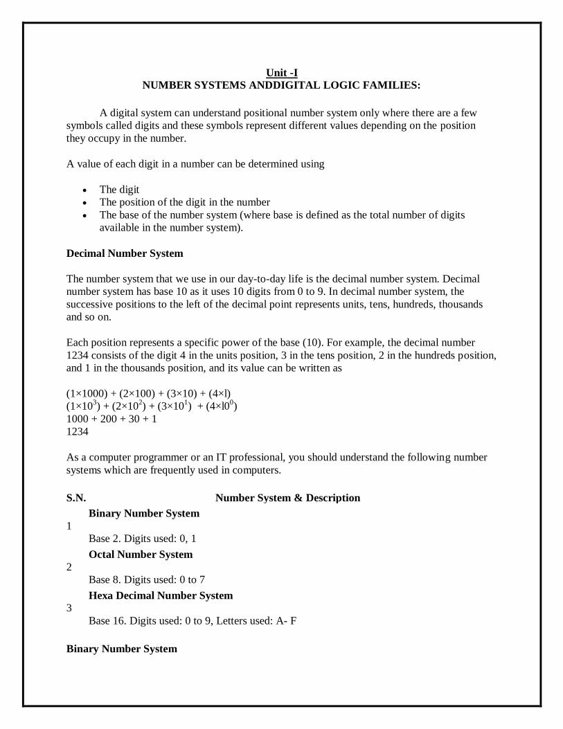
Unit -I
NUMBER SYSTEMS ANDDIGITAL LOGIC FAMILIES:
A digital system can understand positional number system only where there are a few
symbols called digits and these symbols represent different values depending on the position
they occupy in the number.
A value of each digit in a number can be determined using
The digit
The position of the digit in the number
The base of the number system (where base is defined as the total number of digits
available in the number system).
Decimal Number System
The number system that we use in our day-to-day life is the decimal number system. Decimal
number system has base 10 as it uses 10 digits from 0 to 9. In decimal number system, the
successive positions to the left of the decimal point represents units, tens, hundreds, thousands
and so on.
Each position represents a specific power of the base (10). For example, the decimal number
1234 consists of the digit 4 in the units position, 3 in the tens position, 2 in the hundreds position,
and 1 in the thousands position, and its value can be written as
(1×1000) + (2×100) + (3×10) + (4×l)
(1×10³) + (2×10
2) + (3×10
1) + (4×l0
0)
1000 + 200 + 30 + 1
1234
As a computer programmer or an IT professional, you should understand the following number
systems which are frequently used in computers.
S.N. Number System & Description
1
Binary Number System
Base 2. Digits used: 0, 1
2
Octal Number System
Base 8. Digits used: 0 to 7
3 Hexa Decimal Number System
Base 16. Digits used: 0 to 9, Letters used: A- F
Binary Number System
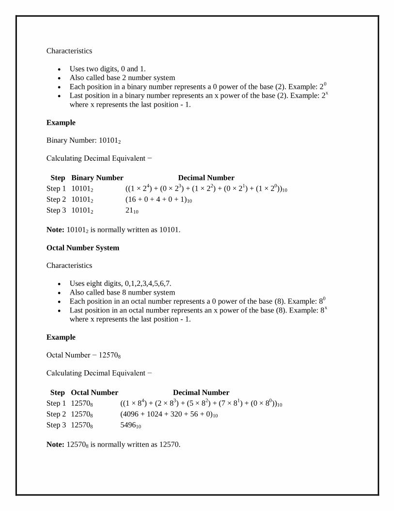
Characteristics
Uses two digits, 0 and 1.
Also called base 2 number system
Each position in a binary number represents a 0 power of the base (2). Example: 20
Last position in a binary number represents an x power of the base (2). Example: 2x
where x represents the last position - 1.
Example
Binary Number: 101012
Calculating Decimal Equivalent −
Step Binary Number Decimal Number
Step 1 101012 ((1 × 24) + (0 × 2
3) + (1 × 2
2) + (0 × 2
1) + (1 × 2
0))10
Step 2 101012 (16 + 0 + 4 + 0 + 1)10
Step 3 101012 2110
Note: 101012 is normally written as 10101.
Octal Number System
Characteristics
Uses eight digits, 0,1,2,3,4,5,6,7.
Also called base 8 number system
Each position in an octal number represents a 0 power of the base (8). Example: 80
Last position in an octal number represents an x power of the base (8). Example: 8x
where x represents the last position - 1.
Example
Octal Number − 125708
Calculating Decimal Equivalent −
Step Octal Number Decimal Number
Step 1 125708 ((1 × 84) + (2 × 8
3) + (5 × 8
2) + (7 × 8
1) + (0 × 8
0))10
Step 2 125708 (4096 + 1024 + 320 + 56 + 0)10
Step 3 125708 549610
Note: 125708 is normally written as 12570.
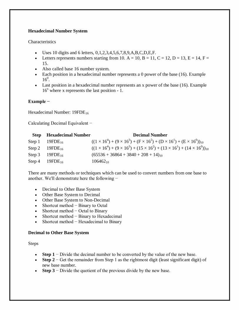
Hexadecimal Number System
Characteristics
Uses 10 digits and 6 letters, 0,1,2,3,4,5,6,7,8,9,A,B,C,D,E,F.
Letters represents numbers starting from 10. A = 10, B = 11, C = 12, D = 13, E = 14, F =
15.
Also called base 16 number system.
Each position in a hexadecimal number represents a 0 power of the base (16). Example
160.
Last position in a hexadecimal number represents an x power of the base (16). Example
16x where x represents the last position - 1.
Example −
Hexadecimal Number: 19FDE16
Calculating Decimal Equivalent −
Step Hexadecimal Number Decimal Number
Step 1 19FDE16 ((1 × 164) + (9 × 16
3) + (F × 16
2) + (D × 16
1) + (E × 16
0))10
Step 2 19FDE16 ((1 × 164) + (9 × 16
3) + (15 × 16
2) + (13 × 16
1) + (14 × 16
0))10
Step 3 19FDE16 (65536 + 36864 + 3840 + 208 + 14)10
Step 4 19FDE16 10646210
There are many methods or techniques which can be used to convert numbers from one base to
another. We'll demonstrate here the following −
Decimal to Other Base System
Other Base System to Decimal
Other Base System to Non-Decimal
Shortcut method − Binary to Octal
Shortcut method − Octal to Binary
Shortcut method − Binary to Hexadecimal
Shortcut method − Hexadecimal to Binary
Decimal to Other Base System
Steps
Step 1 − Divide the decimal number to be converted by the value of the new base.
Step 2 − Get the remainder from Step 1 as the rightmost digit (least significant digit) of
new base number.
Step 3 − Divide the quotient of the previous divide by the new base.
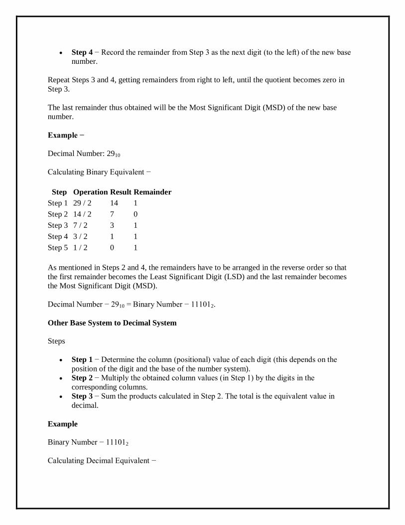
Step 4 − Record the remainder from Step 3 as the next digit (to the left) of the new base
number.
Repeat Steps 3 and 4, getting remainders from right to left, until the quotient becomes zero in
Step 3.
The last remainder thus obtained will be the Most Significant Digit (MSD) of the new base
number.
Example −
Decimal Number: 2910
Calculating Binary Equivalent −
Step Operation Result Remainder
Step 1 29 / 2 14 1
Step 2 14 / 2 7 0
Step 3 7 / 2 3 1
Step 4 3 / 2 1 1
Step 5 1 / 2 0 1
As mentioned in Steps 2 and 4, the remainders have to be arranged in the reverse order so that
the first remainder becomes the Least Significant Digit (LSD) and the last remainder becomes
the Most Significant Digit (MSD).
Decimal Number − 2910 = Binary Number − 111012.
Other Base System to Decimal System
Steps
Step 1 − Determine the column (positional) value of each digit (this depends on the
position of the digit and the base of the number system).
Step 2 − Multiply the obtained column values (in Step 1) by the digits in the
corresponding columns.
Step 3 − Sum the products calculated in Step 2. The total is the equivalent value in
decimal.
Example
Binary Number − 111012
Calculating Decimal Equivalent −
Step Binary Number Decimal Number
Step 1 111012 ((1 × 24) + (1 × 2
3) + (1 × 2
2) + (0 × 2
1) + (1 × 2
0))10
Step 2 111012 (16 + 8 + 4 + 0 + 1)10
Step 3 111012 2910
Binary Number − 111012 = Decimal Number − 2910
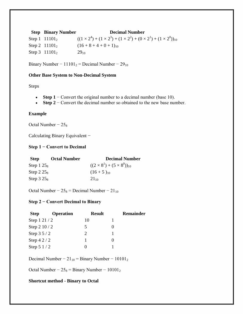
Other Base System to Non-Decimal System
Steps
Step 1 − Convert the original number to a decimal number (base 10).
Step 2 − Convert the decimal number so obtained to the new base number.
Example
Octal Number − 258
Calculating Binary Equivalent −
Step 1 − Convert to Decimal
Step Octal Number Decimal Number
Step 1 258 ((2 × 81) + (5 × 8
0))10
Step 2 258 (16 + 5 )10
Step 3 258 2110
Octal Number − 258 = Decimal Number − 2110
Step 2 − Convert Decimal to Binary
Step Operation Result Remainder
Step 1 21 / 2 10 1
Step 2 10 / 2 5 0
Step 3 5 / 2 2 1
Step 4 2 / 2 1 0
Step 5 1 / 2 0 1
Decimal Number − 2110 = Binary Number − 101012
Octal Number − 258 = Binary Number − 101012
Shortcut method - Binary to Octal
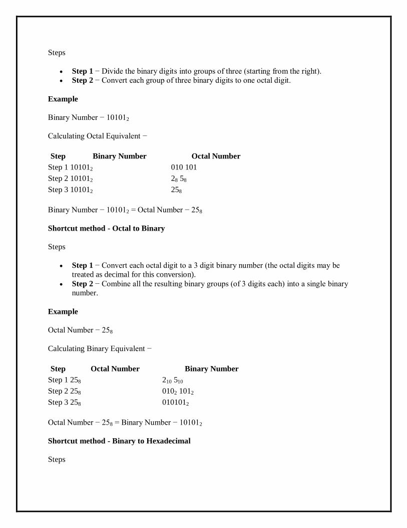
Steps
Step 1 − Divide the binary digits into groups of three (starting from the right).
Step 2 − Convert each group of three binary digits to one octal digit.
Example
Binary Number − 101012
Calculating Octal Equivalent −
Step Binary Number Octal Number
Step 1 101012 010 101
Step 2 101012 28 58
Step 3 101012 258
Binary Number − 101012 = Octal Number − 258
Shortcut method - Octal to Binary
Steps
Step 1 − Convert each octal digit to a 3 digit binary number (the octal digits may be
treated as decimal for this conversion).
Step 2 − Combine all the resulting binary groups (of 3 digits each) into a single binary
number.
Example
Octal Number − 258
Calculating Binary Equivalent −
Step Octal Number Binary Number
Step 1 258 210 510
Step 2 258 0102 1012
Step 3 258 0101012
Octal Number − 258 = Binary Number − 101012
Shortcut method - Binary to Hexadecimal
Steps
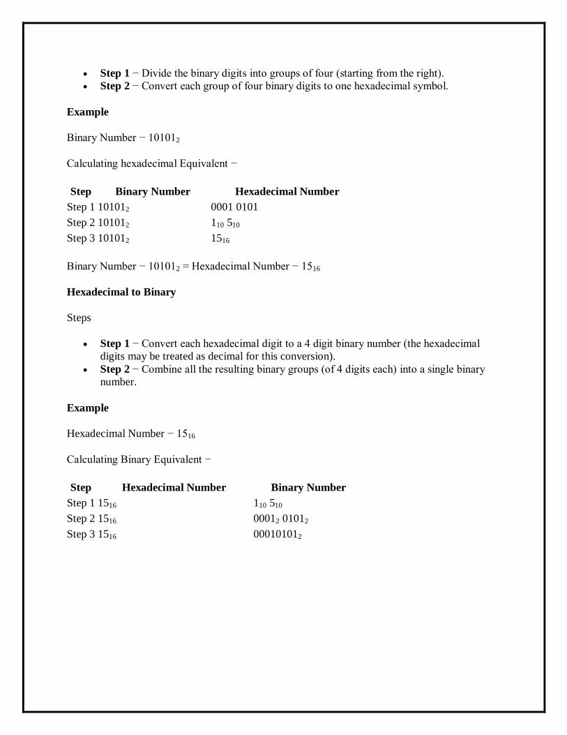
Step 1 − Divide the binary digits into groups of four (starting from the right).
Step 2 − Convert each group of four binary digits to one hexadecimal symbol.
Example
Binary Number − 101012
Calculating hexadecimal Equivalent −
Step Binary Number Hexadecimal Number
Step 1 101012 0001 0101
Step 2 101012 110 510
Step 3 101012 1516
Binary Number − 101012 = Hexadecimal Number − 1516
Hexadecimal to Binary
Steps
Step 1 − Convert each hexadecimal digit to a 4 digit binary number (the hexadecimal
digits may be treated as decimal for this conversion).
Step 2 − Combine all the resulting binary groups (of 4 digits each) into a single binary
number.
Example
Hexadecimal Number − 1516
Calculating Binary Equivalent −
Step Hexadecimal Number Binary Number
Step 1 1516 110 510
Step 2 1516 00012 01012
Step 3 1516 000101012
In the coding, when numbers, letters or words are represented by a specific group of
symbols, it is said that the number, letter or word is being encoded. The group of symbols is
called as a code. The digital data is represented, stored and transmitted as group of binary bits.
This group is also called as binary code. The binary code is represented by the number as well
as alphanumeric letter.
Advantages of Binary Code
Following is the list of advantages that binary code offers.
Binary codes are suitable for the computer applications.
Binary codes are suitable for the digital communications.
Binary codes make the analysis and designing of digital circuits if we use the binary
codes.
Since only 0 & 1 are being used, implementation becomes easy.
Classification of binary codes
The codes are broadly categorized into following four categories.
Weighted Codes
Non-Weighted Codes
Binary Coded Decimal Code
Alphanumeric Codes
Error Detecting Codes
Error Correcting Codes
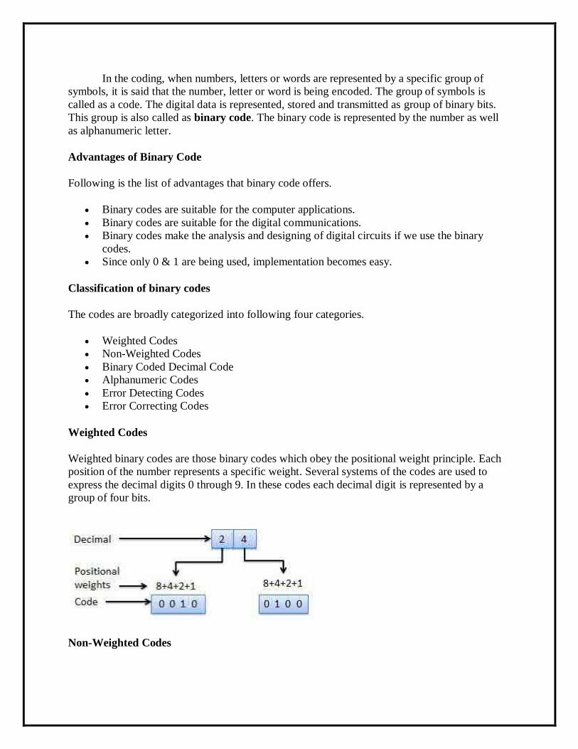
Weighted Codes
Weighted binary codes are those binary codes which obey the positional weight principle. Each
position of the number represents a specific weight. Several systems of the codes are used to
express the decimal digits 0 through 9. In these codes each decimal digit is represented by a
group of four bits.
Non-Weighted Codes
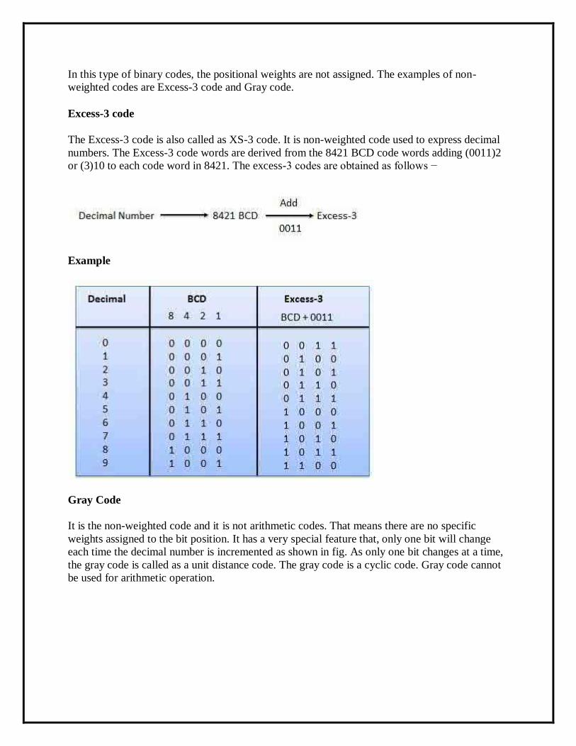
In this type of binary codes, the positional weights are not assigned. The examples of non-
weighted codes are Excess-3 code and Gray code.
Excess-3 code
The Excess-3 code is also called as XS-3 code. It is non-weighted code used to express decimal
numbers. The Excess-3 code words are derived from the 8421 BCD code words adding (0011)2
or (3)10 to each code word in 8421. The excess-3 codes are obtained as follows −
Example
Gray Code
It is the non-weighted code and it is not arithmetic codes. That means there are no specific
weights assigned to the bit position. It has a very special feature that, only one bit will change
each time the decimal number is incremented as shown in fig. As only one bit changes at a time,
the gray code is called as a unit distance code. The gray code is a cyclic code. Gray code cannot
be used for arithmetic operation.
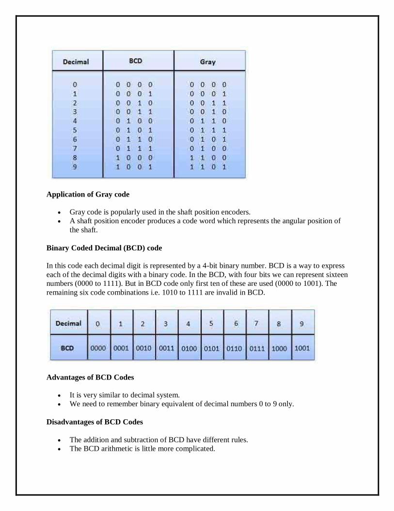
Application of Gray code
Gray code is popularly used in the shaft position encoders.
A shaft position encoder produces a code word which represents the angular position of
the shaft.
Binary Coded Decimal (BCD) code
In this code each decimal digit is represented by a 4-bit binary number. BCD is a way to express
each of the decimal digits with a binary code. In the BCD, with four bits we can represent sixteen
numbers (0000 to 1111). But in BCD code only first ten of these are used (0000 to 1001). The
remaining six code combinations i.e. 1010 to 1111 are invalid in BCD.
Advantages of BCD Codes
It is very similar to decimal system.
We need to remember binary equivalent of decimal numbers 0 to 9 only.
Disadvantages of BCD Codes
The addition and subtraction of BCD have different rules.
The BCD arithmetic is little more complicated.

BCD needs more number of bits than binary to represent the decimal number. So BCD is
less efficient than binary.
Alphanumeric codes
A binary digit or bit can represent only two symbols as it has only two states '0' or '1'. But this is
not enough for communication between two computers because there we need many more
symbols for communication. These symbols are required to represent 26 alphabets with capital
and small letters, numbers from 0 to 9, punctuation marks and other symbols.
The alphanumeric codes are the codes that represent numbers and alphabetic characters. Mostly
such codes also represent other characters such as symbol and various instructions necessary for
conveying information. An alphanumeric code should at least represent 10 digits and 26 letters
of alphabet i.e. total 36 items. The following three alphanumeric codes are very commonly used
for the data representation.
American Standard Code for Information Interchange (ASCII).
Extended Binary Coded Decimal Interchange Code (EBCDIC).
Five bit Baudot Code.
ASCII code is a 7-bit code whereas EBCDIC is an 8-bit code. ASCII code is more commonly
used worldwide while EBCDIC is used primarily in large IBM computers.
Error Codes
There are binary code techniques available to detect and correct data during data transmission.
Error Code Description
Error Detection and Correction Error detection and correction code techniques
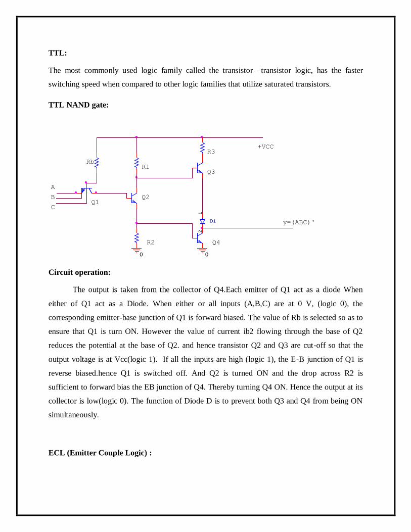
TTL:
The most commonly used logic family called the transistor –transistor logic, has the faster
switching speed when compared to other logic families that utilize saturated transistors.
TTL NAND gate:
Circuit operation:
The output is taken from the collector of Q4.Each emitter of Q1 act as a diode When
either of Q1 act as a Diode. When either or all inputs (A,B,C) are at 0 V, (logic 0), the
corresponding emitter-base junction of Q1 is forward biased. The value of Rb is selected so as to
ensure that Q1 is turn ON. However the value of current ib2 flowing through the base of Q2
reduces the potential at the base of Q2. and hence transistor Q2 and Q3 are cut-off so that the
output voltage is at Vcc(logic 1). If all the inputs are high (logic 1), the E-B junction of Q1 is
reverse biased.hence Q1 is switched off. And Q2 is turned ON and the drop across R2 is
sufficient to forward bias the EB junction of Q4. Thereby turning Q4 ON. Hence the output at its
collector is low(logic 0). The function of Diode D is to prevent both Q3 and Q4 from being ON
simultaneously.
ECL (Emitter Couple Logic) :
R3
y=(ABC)'
BQ1
0
A
+VCC
Q3
C
R1
D1
12
R2 Q4
Q2
0
Rb
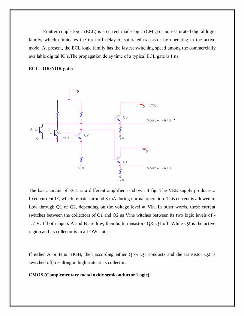
Emitter couple logic (ECL) is a current mode logic (CML) or non-saturated digital logic
family, which eliminates the turn off delay of saturated transistor by operating in the active
mode. At present, the ECL logic family has the fastest switching speed among the commercially
available digital IC‟s.The propagation delay time of a typical ECL gate is 1 ns.
ECL - OR/NOR gate:
The basic circuit of ECL is a different amplifier as shown if fig. The VEE supply produces a
fixed current IE, which remains around 3 mA during normal operation. This current is allowed to
flow through Q1 or Q2, depending on the voltage level at Vin. In other words, these current
switches between the collectors of Q1 and Q2 as Vine witches between its two logic levels of -
1.7 V. If both inputs A and B are low, then both transistors Q& Q1 off. While Q2 is the active
region and its collector is in a LOW state.
If either A or B is HIGH, then according either Q or Q1 conducts and the transistor Q2 is
switched off, resulting in high state at its collector.
CMOS (Complementary metal oxide semiconductor Logic)
-2v
B
0
Q
Vout= (A+B)'
-2v
VEE
0
0
A
+VCC
Q1
-1.3 vQ2
Vout= (A+B)
Q4
Q3
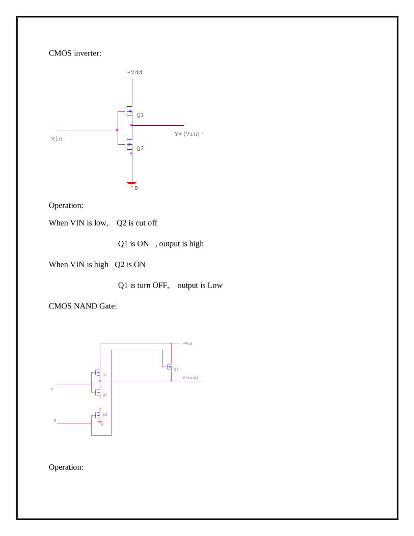
CMOS inverter:
Operation:
When VIN is low, Q2 is cut off
Q1 is ON , output is high
When VIN is high Q2 is ON
Q1 is turn OFF, output is Low
CMOS NAND Gate:
Operation:
0
Q2
Y=(Vin)'
+Vdd
Q1
Vin
Q2
Y=(A.B)
0
Q4
+Vdd
Q3
B
Q1
A

If both input is High, both P channel transistor turned off and boths „n‟ channel transistors turned
ON. The output has a low impedance to ground and produces a low state.
If any input is low, the associated n-channel transisitor is turned off. And the associated p-
channel transisitor is turned ON.The output is coupled to VDD and goes to the HIGH state.
To produce the positive AND function the output of the CMOS NAND gate can be connected to
a CMOS inverter.
UNIT II
BOOLEAN ALGEBRA AND COMBINATIONAL CIRCUITS
Boolean Algebra:
Properties of Boolean algebra:
commutative property:
A+B=B+A
A.B=B.A
Associative property:
A+(B+C) = (A+B)+C
A.(B.C) =(A.B)C
Distributive property:
A+BC=(A+B)(A+C)
A.(B+C) = A.B+A.C
Absorption laws:
A+AB = A
A.(A+B)
A+A‟B = A+B
A.(A‟+B) = AB
Consensus Laws:
AB + A‟C + BC = AB + A‟C
(A+B)(A‟+C)(B+C) = (A+B)(A‟+C)
other laws of Boolean algebra:
A+0 =A A.1= A
A+1=1 A.0=0
A+A=A A.A=A
A+A‟=1 A.A‟=0
A‟‟=A A‟‟=A
Principle of duality:
From the above properties and laws of Boolean algebra, it is evident that they are
grouped in pairs. One expression can be obtained from the other in each pair by replacing every
0 with 1, every 1 with 0, every + with . every . with +. Any pair of expression satisfying this
property is called dual expression. This characteristics of Boolean algebra is called the principles
of duality.
De-Morgan’s theorem:
(AB)‟=A‟+B‟
The complement of a product is equal to the sum of the compliments.
(A+B)‟= A‟.B‟
The complement of a sum is equal to the product of the complements.
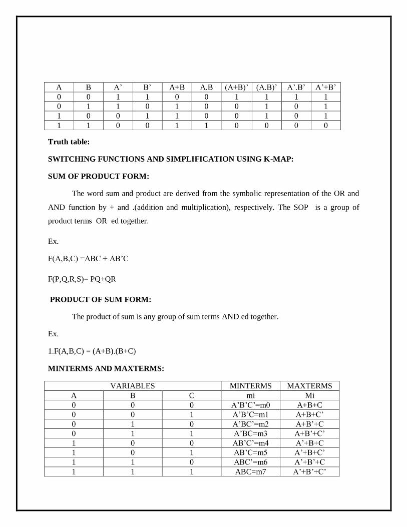
Truth table:
SWITCHING FUNCTIONS AND SIMPLIFICATION USING K-MAP:
SUM OF PRODUCT FORM:
The word sum and product are derived from the symbolic representation of the OR and
AND function by + and .(addition and multiplication), respectively. The SOP is a group of
product terms OR ed together.
Ex.
F(A,B,C) =ABC + AB‟C
F(P,Q,R,S)= PQ+QR
PRODUCT OF SUM FORM:
The product of sum is any group of sum terms AND ed together.
Ex.
1.F(A,B,C) = (A+B).(B+C)
MINTERMS AND MAXTERMS:
VARIABLES MINTERMS MAXTERMS
A B C mi Mi
0 0 0 A‟B‟C‟=m0 A+B+C
0 0 1 A‟B‟C=m1 A+B+C‟
0 1 0 A‟BC‟=m2 A+B‟+C
0 1 1 A‟BC=m3 A+B‟+C‟
1 0 0 AB‟C‟=m4 A‟+B+C
1 0 1 AB‟C=m5 A‟+B+C‟
1 1 0 ABC‟=m6 A‟+B‟+C
1 1 1 ABC=m7 A‟+B‟+C‟
A B A‟ B‟ A+B A.B (A+B)‟ (A.B)‟ A‟.B‟ A‟+B‟
0 0 1 1 0 0 1 1 1 1
0 1 1 0 1 0 0 1 0 1
1 0 0 1 1 0 0 1 0 1
1 1 0 0 1 1 0 0 0 0
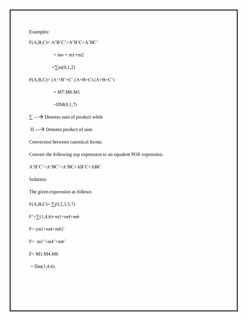
Examples:
F(A,B,C)= A‟B‟C‟+A‟B‟C+A‟BC‟
= mo + m1+m2
=∑m(0,1,2)
F(A,B,C)= (A‟+B‟+C‟.(A+B+C).(A+B+C‟)
= M7.M0.M1
=ΠM(0,1,7)
∑ --- Denotes sum of product while
Π --- Denotes product of sum
Conversion between canonical forms:
Convert the following sop expression to an equalent POS expression.
A‟B‟C‟+A‟BC‟+A‟BC+AB‟C+ABC
Solution:
The given expression as follows
F(A,B,C)= ∑(0,2,3,5,7)
F‟=∑(1,4,6)=m1+m4+m6
F= (m1+m4+m6)‟
F= m1‟+m4‟+m6‟
F= M1.M4.M6
= Πm(1,4,6).
STRUCTURE OF K MAP:
EXAMPLE 1
Simplify the following function using K map for 4 variables a,b,c,d.
1410
2
0
THREE VARIABLE KMAP
AB00
B
0
10
3
2
0
1
CD
15
6
10
FOUR VARIABLE KMAP
1
5
11
0 11
01
6
1
11
3
01 5
7
10
12
1
0
AB
800
TWO VARIABLE K MAP
00C
9
A
3
1
2
4
13
11
7
01
4
1
10
AB00
1
1
CD
0
1
1101
1
1
01
1 0
10
00
0
00 0
1
0
0
11
Y=AC‟+A‟D
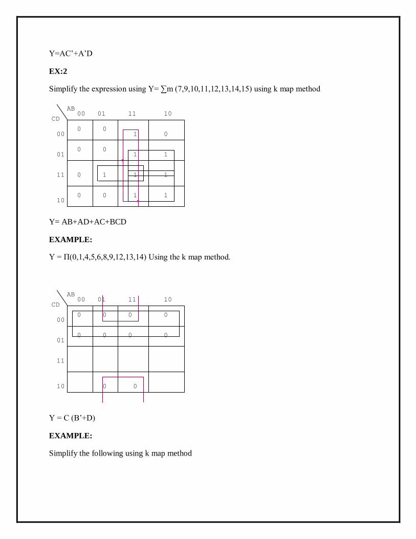
EX:2
Simplify the expression using Y= ∑m (7,9,10,11,12,13,14,15) using k map method
Y= AB+AD+AC+BCD
EXAMPLE:
Y = Π(0,1,4,5,6,8,9,12,13,14) Using the k map method.
Y = C (B‟+D)
EXAMPLE:
Simplify the following using k map method
1
10
AB00
1
1
CD
0
0
1101
1 1
01
1
0
10
1
0
0
000
1
0
0
11
10
AB00
CD
0 0
1101
01
0
0
10
0 000
00
0
0
11
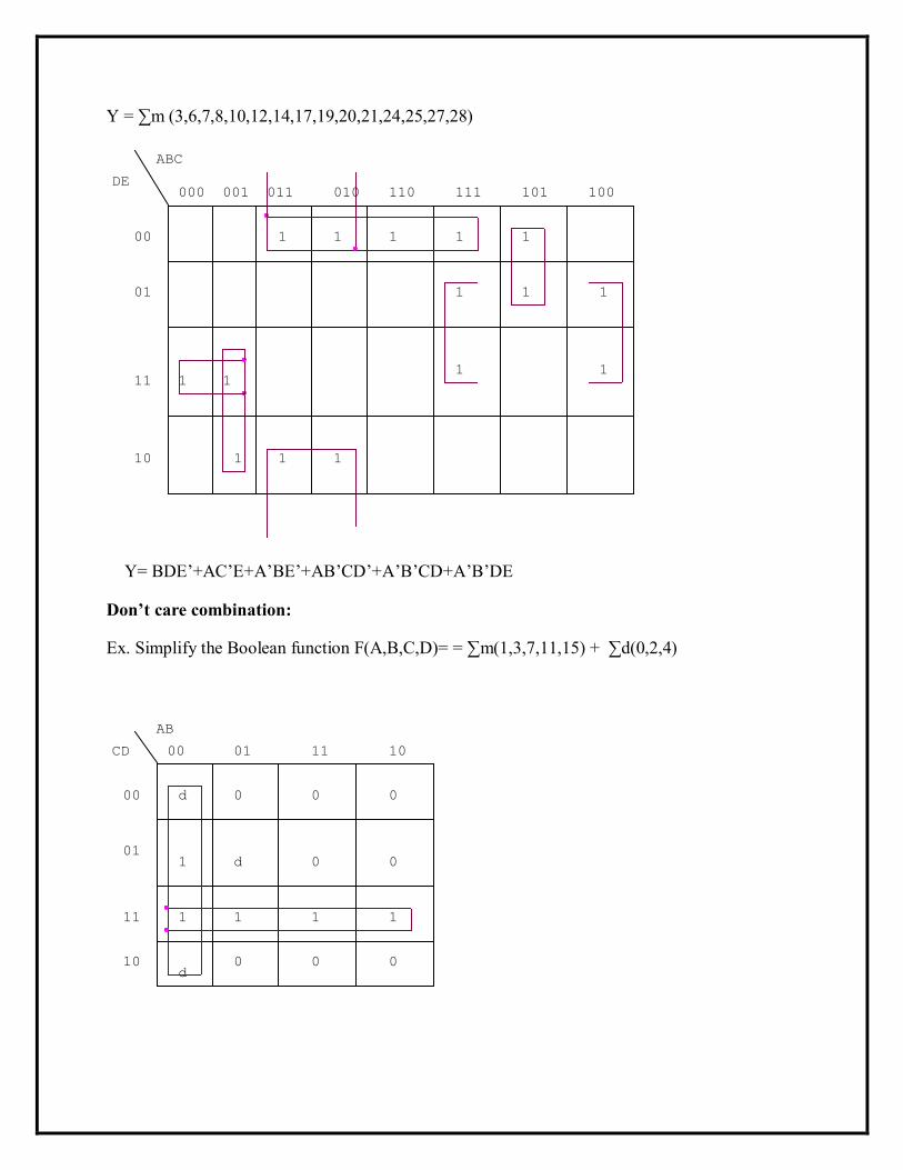
Y = ∑m (3,6,7,8,10,12,14,17,19,20,21,24,25,27,28)
Y= BDE‟+AC‟E+A‟BE‟+AB‟CD‟+A‟B‟CD+A‟B‟DE
Don’t care combination:
Ex. Simplify the Boolean function F(A,B,C,D)= = ∑m(1,3,7,11,15) + ∑d(0,2,4)
1
11
1
1 1
1
1
1
1
11
010 101
1
001
10
111
1
011
1
1
110 100
1
ABC
DE
00
000
01
0
10
CD
0 0
d
0
AB
11
d
01
0
1
d
01
1
00
0
10
1 1
000
11 1
0
Y= A‟B‟ + CD
Example:
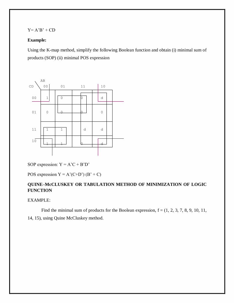
Using the K-map method, simplify the following Boolean function and obtain (i) minimal sum of
products (SOP) (ii) minimal POS expression
SOP expression: Y = A‟C + B‟D‟
POS expression Y = A‟(C+D‟) (B‟ + C)
QUINE–McCLUSKEY OR TABULATION METHOD OF MINIMIZATION OF LOGIC
FUNCTION
EXAMPLE:
Find the minimal sum of products for the Boolean expression, f = (1, 2, 3, 7, 8, 9, 10, 11,
14, 15), using Quine McCluskey method.
10
CD
0
01 d0
0 0
d1
0
AB
1
d
1101
d
1
01
00
1
10
0
00
11
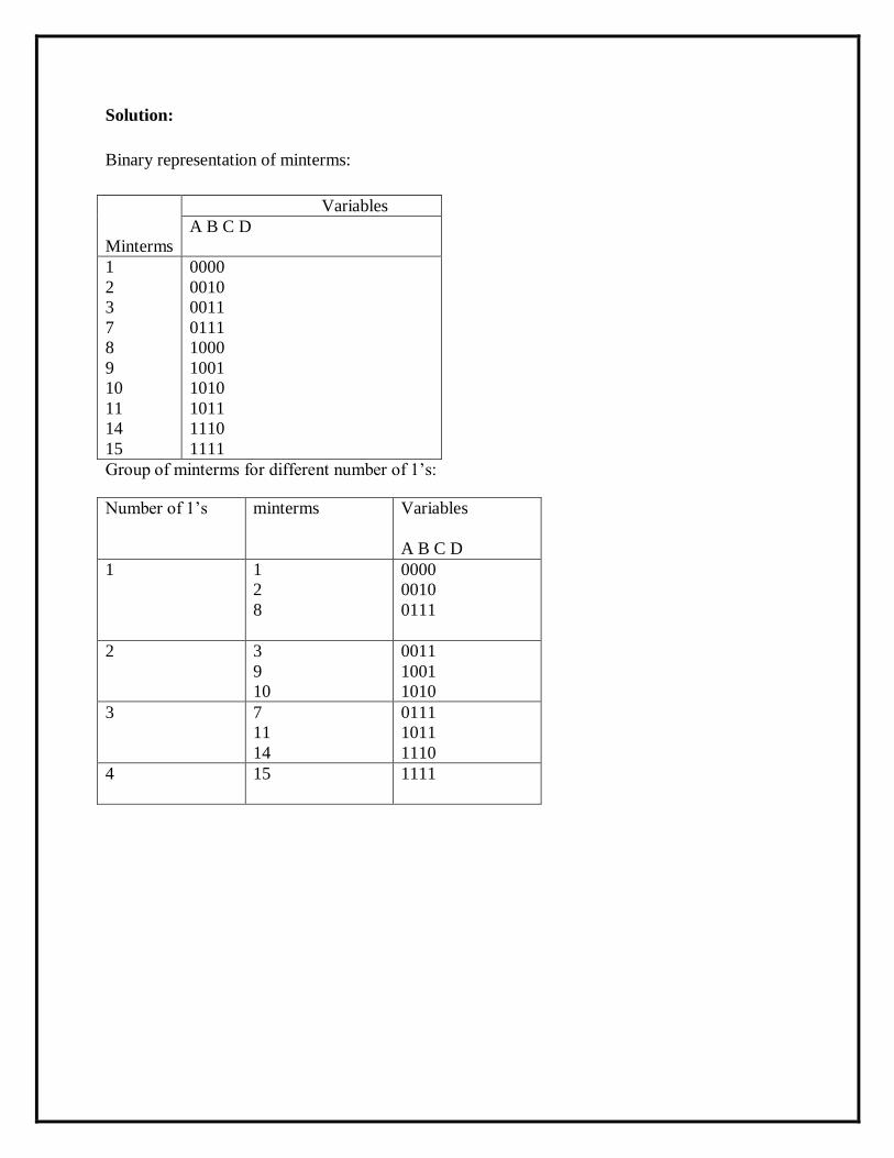
Solution:
Binary representation of minterms:
Minterms
Variables
A B C D
1
2
3
7
8
9
10
11
14
15
0000
0010
0011
0111
1000
1001
1010
1011
1110
1111
Group of minterms for different number of 1‟s:
Number of 1‟s minterms Variables
A B C D
1 1
2
8
0000
0010
0111
2 3
9
10
0011
1001
1010
3 7
11
14
0111
1011
1110
4 15
1111
2 CELL COMBINATION:
COMBINATION A B C D
1,3
1,9
2,3
2,10
8,9
8,10
00-1
-001
001-
-010
100-
10-0
3,7
3,11
9,11
10,11
10,14
0-11
-011
10-1
101-
1-10
7,15
11,15
14,15
-111
1-11
111-
4 cell combination
COMBINATION A B C D
1,3,9,11
2,3,10,11
8,9,10,11
-0-1
-01-
10--
3,7,11,15
10,11,14,15
--11
1-1-
PRIME IMPLICANT CHART:
PRIME
IMPLICANTS
MINTERMS
1 2 3 7 8 9 10 11 14 15
(1,3,9,11)*
(2,3,10,11)*
(8,9,10,11)*
(3,7,11,15)*
(10,11,14,15)*
X
X
X
X
X
X
X
X
X
X
X
X
X
X
X
X
X
X
X
X
F = B‟.D + B‟ .C + A.B‟ +C.D + A.C
Combinational logic:
Digital computers and calculators consists of arithmetic and logic circuits, which contains logic
gates and flip flops that add, subtract, multiply and divide binary numbers.
In Combinational logic circuit, the output at any time depends only on present input values at
that time.
Half adder:
Truth table:
A B sum carry
0 0 0 0
0 1 1 0
1 0 1 0
1 1 0 1
Sum= A‟B+AB‟
Carry= A.B
Logic diagram:
U2A
7408
1
23
A
SUM
U1A
7486
1
23
B
CARRY
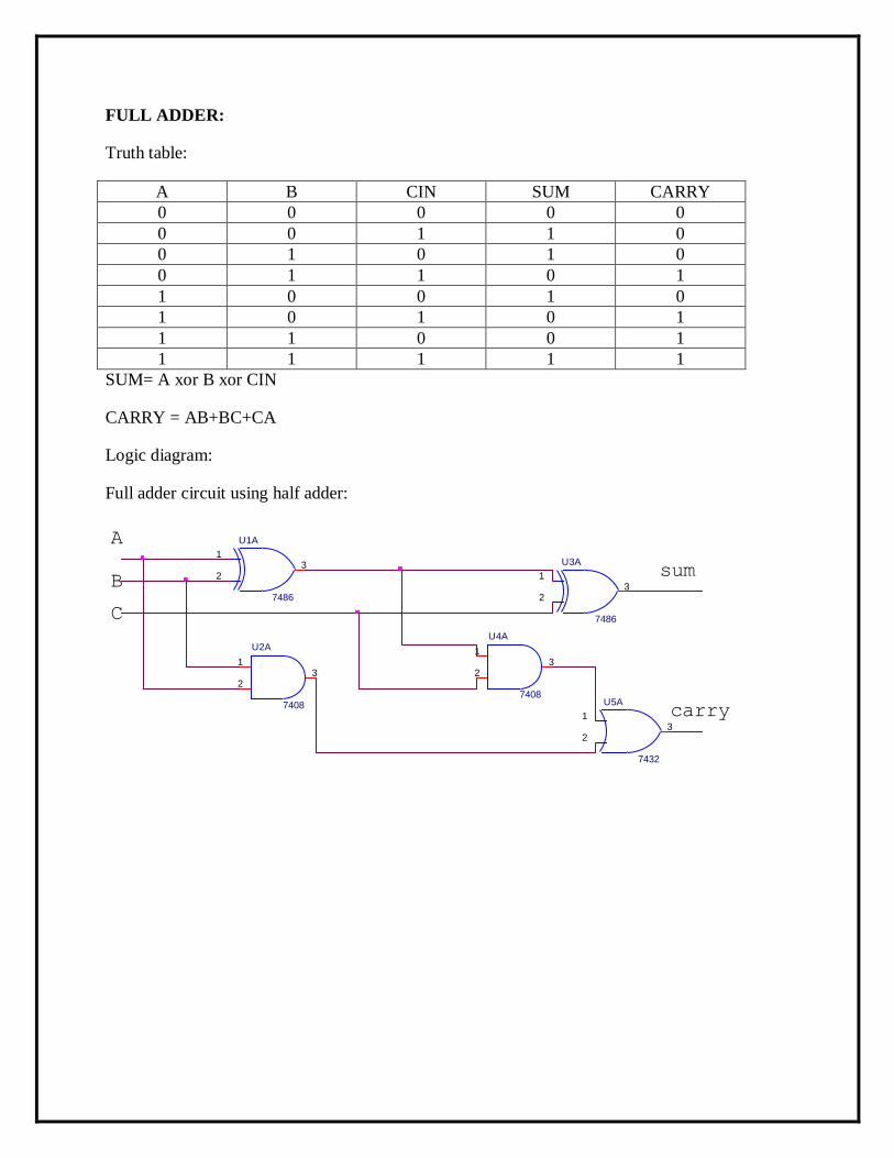
FULL ADDER:
Truth table:
A B CIN SUM CARRY
0 0 0 0 0
0 0 1 1 0
0 1 0 1 0
0 1 1 0 1
1 0 0 1 0
1 0 1 0 1
1 1 0 0 1
1 1 1 1 1
SUM= A xor B xor CIN
CARRY = AB+BC+CA
Logic diagram:
Full adder circuit using half adder:
C
U1A
7486
1
23
U4A
7408
1
23
B
U2A
7408
1
23
carryU5A
7432
1
23
A
sumU3A
7486
1
23
Half subtractor :
Truth table
A B Difference Borrow
0 0 0 0
0 1 1 1
1 0 1 0
1 1 0 0
Differece = A xor B
Borrow = A‟B
Logic diagram:
Full subtractor:
Truth table:
A B Bin difference Borrow
0 0 0 0 0
0 0 1 1 1
0 1 0 1 1
0 1 1 0 1
1 0 0 1 0
1 0 1 0 0
1 1 0 0 0
1 1 1 1 1
Difference = A xor B xor Bin
Borrow = A‟B + BC + CA‟
U1A
7486
1
23
U6A
7404
12
Borrow
B
difference
U2A
7408
1
23
A
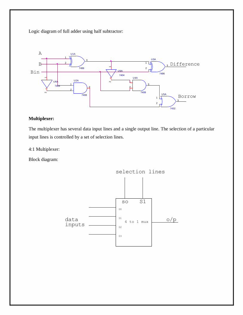
Logic diagram of full adder using half subtractor:
Multiplexer:
The multiplexer has several data input lines and a single output line. The selection of a particular
input lines is controlled by a set of selection lines.
4:1 Multiplexer:
Block diagram:
Difference
Bin
U1A
7486
1
23
U6A
7404
12
U4A
7408
1
23
B
Borrow
U2A
7408
1
23
U6A
7404
12
U5A
7432
1
23
A
U3A
7486
1
23
D2
D1
4 to 1 mux
so
selection lines
o/p
D0
D3
datainputs
S1
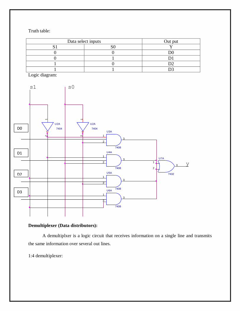
Truth table:
Data select inputs Out put
S1 S0 Y
0 0 D0
0 1 D1
1 0 D2
1 1 D3
Logic diagram:
Demultiplexer (Data distributors):
A demultiplxer is a logic circuit that receives information on a single line and transmits
the same information over several out lines.
1:4 demultiplexer:
U4A
7408
1
23
s1
U5A
7408
1
23
s0
U2A
7404
12
y
U3A
7408
1
23
U6A
7408
1
23
U7A
7432
1
23
U2A
7404
12
D0
D1
D2
D3
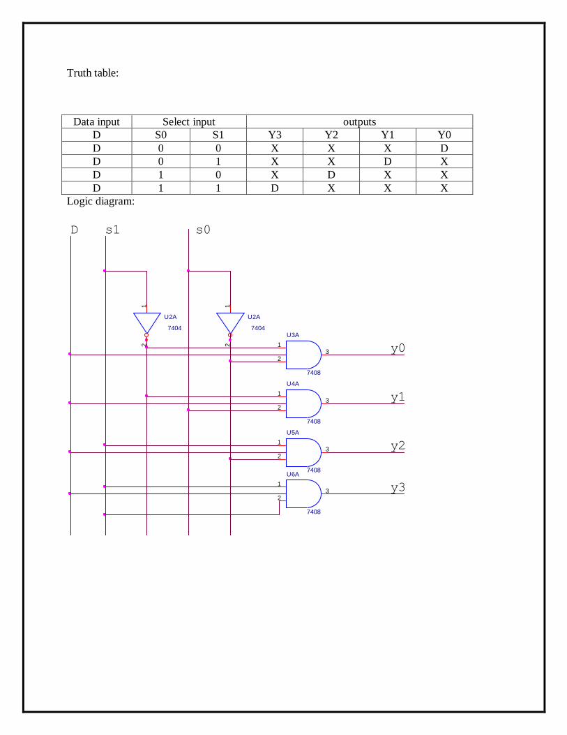
Truth table:
Data input Select input outputs
D S0 S1 Y3 Y2 Y1 Y0
D 0 0 X X X D
D 0 1 X X D X
D 1 0 X D X X
D 1 1 D X X X
Logic diagram:
U4A
7408
1
23
s1
U5A
7408
1
23
s0
y1
y0
U2A
7404
12
D
y2
U3A
7408
1
23
y3
U6A
7408
1
23
U2A
7404
12
Decoder:
A decoder is similar to demultiplexer but without any data input. In a decoder, the
number of outputs is greater than the number of inputs.
3:8 decoder:
A 3:8 decoder has three inputs and eight outputs . the truth table and logic diagram are
follows.
Truth table:
Inputs outputs
A B C D0 D1 D2 D3 D4 D5 D6 D7
0 0 0 1 0 0 0 0 0 0 0
0 0 1 0 1 0 0 0 0 0 0
0 1 0 0 0 1 0 0 0 0 0
0 1 1 0 0 0 1 0 0 0 0
1 0 0 0 0 0 0 1 0 0 0
1 0 1 0 0 0 0 0 1 0 0
1 1 0 0 0 0 0 0 0 1 0
1 1 1 0 0 0 0 0 0 0 1
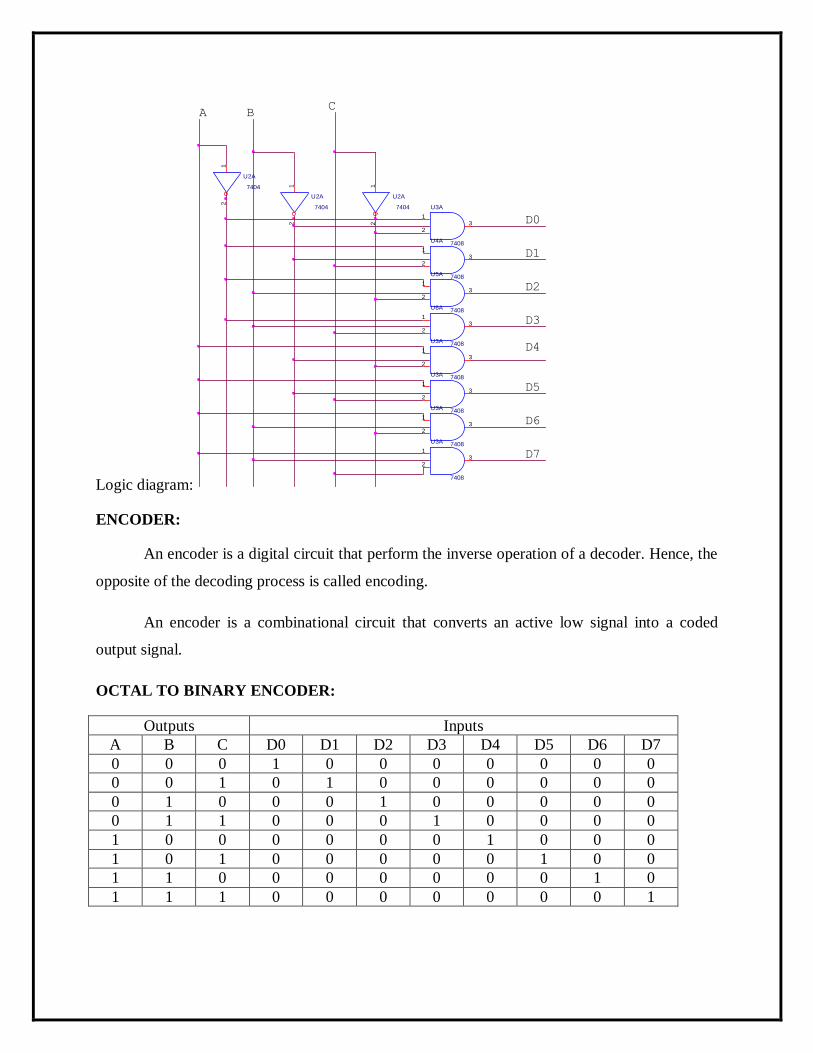
Logic diagram:
ENCODER:
An encoder is a digital circuit that perform the inverse operation of a decoder. Hence, the
opposite of the decoding process is called encoding.
An encoder is a combinational circuit that converts an active low signal into a coded
output signal.
OCTAL TO BINARY ENCODER:
Outputs Inputs
A B C D0 D1 D2 D3 D4 D5 D6 D7
0 0 0 1 0 0 0 0 0 0 0
0 0 1 0 1 0 0 0 0 0 0
0 1 0 0 0 1 0 0 0 0 0
0 1 1 0 0 0 1 0 0 0 0
1 0 0 0 0 0 0 1 0 0 0
1 0 1 0 0 0 0 0 1 0 0
1 1 0 0 0 0 0 0 0 1 0
1 1 1 0 0 0 0 0 0 0 1
D2
U4A
7408
1
23
D7
U3A
7408
1
23
U5A
7408
1
23
D4
U2A
7404
12
D0
A B
U2A
7404
12
D3
U3A
7408
1
23
D1
D6
C
U3A
7408
1
23
D5
U6A
7408
1
23
U3A
7408
1
23
U2A
7404
12
U3A
7408
1
23
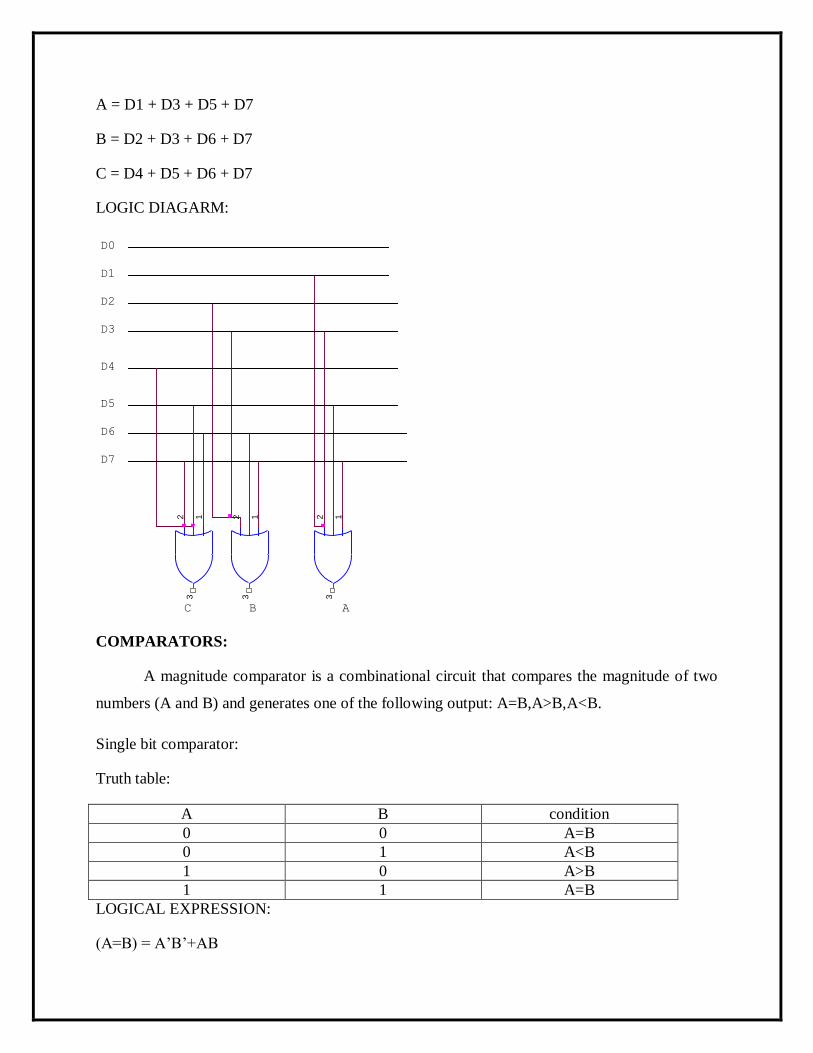
A = D1 + D3 + D5 + D7
B = D2 + D3 + D6 + D7
C = D4 + D5 + D6 + D7
LOGIC DIAGARM:
COMPARATORS:
A magnitude comparator is a combinational circuit that compares the magnitude of two
numbers (A and B) and generates one of the following output: A=B,A>B,A<B.
Single bit comparator:
Truth table:
A B condition
0 0 A=B
0 1 A<B
1 0 A>B
1 1 A=B
LOGICAL EXPRESSION:
(A=B) = A‟B‟+AB
B
D5
123
A
D7
C
D6
D1
123
D0
D4
D2
123
D3
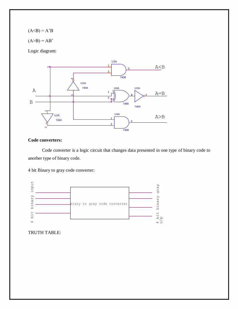
(A<B) = A‟B
(A>B) = AB‟
Logic diagram:
Code converters:
Code converter is a logic circuit that changes data presented in one type of binary code to
another type of binary code.
4 bit Binary to gray code converter:
TRUTH TABLE:
A
A>B
A=B
U2A
7404
12
U2A
7404
1 2
U3A
7408
1
23
U4A
7486
1
23
U3A
7408
1
23
U2A
7404
12
B
A<B
4 bit binary input
4 bit binary gray
o/p
biary to gray code converter
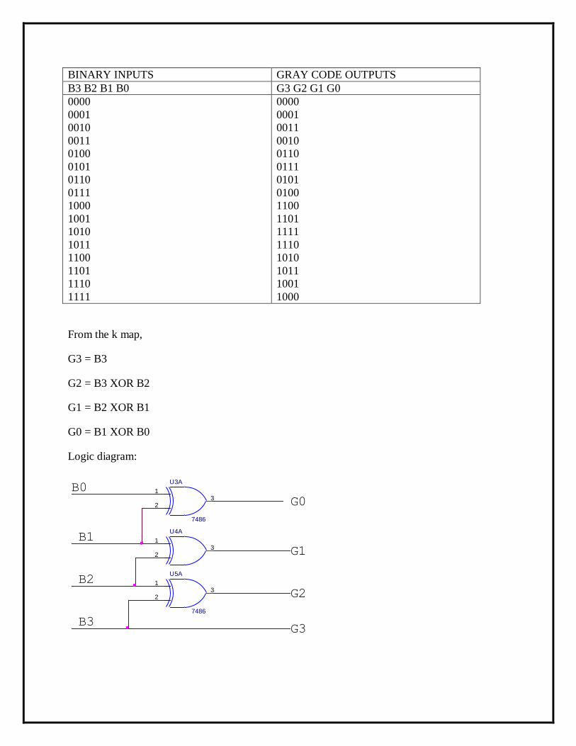
BINARY INPUTS GRAY CODE OUTPUTS
B3 B2 B1 B0 G3 G2 G1 G0
0000
0001
0010
0011
0100
0101
0110
0111
1000
1001
1010
1011
1100
1101
1110
1111
0000
0001
0011
0010
0110
0111
0101
0100
1100
1101
1111
1110
1010
1011
1001
1000
From the k map,
G3 = B3
G2 = B3 XOR B2
G1 = B2 XOR B1
G0 = B1 XOR B0
Logic diagram:
G2
G3
B0
B3
B1
B2
U3A
7486
1
23
G1
U4A
1
23
G0
U5A
7486
1
23
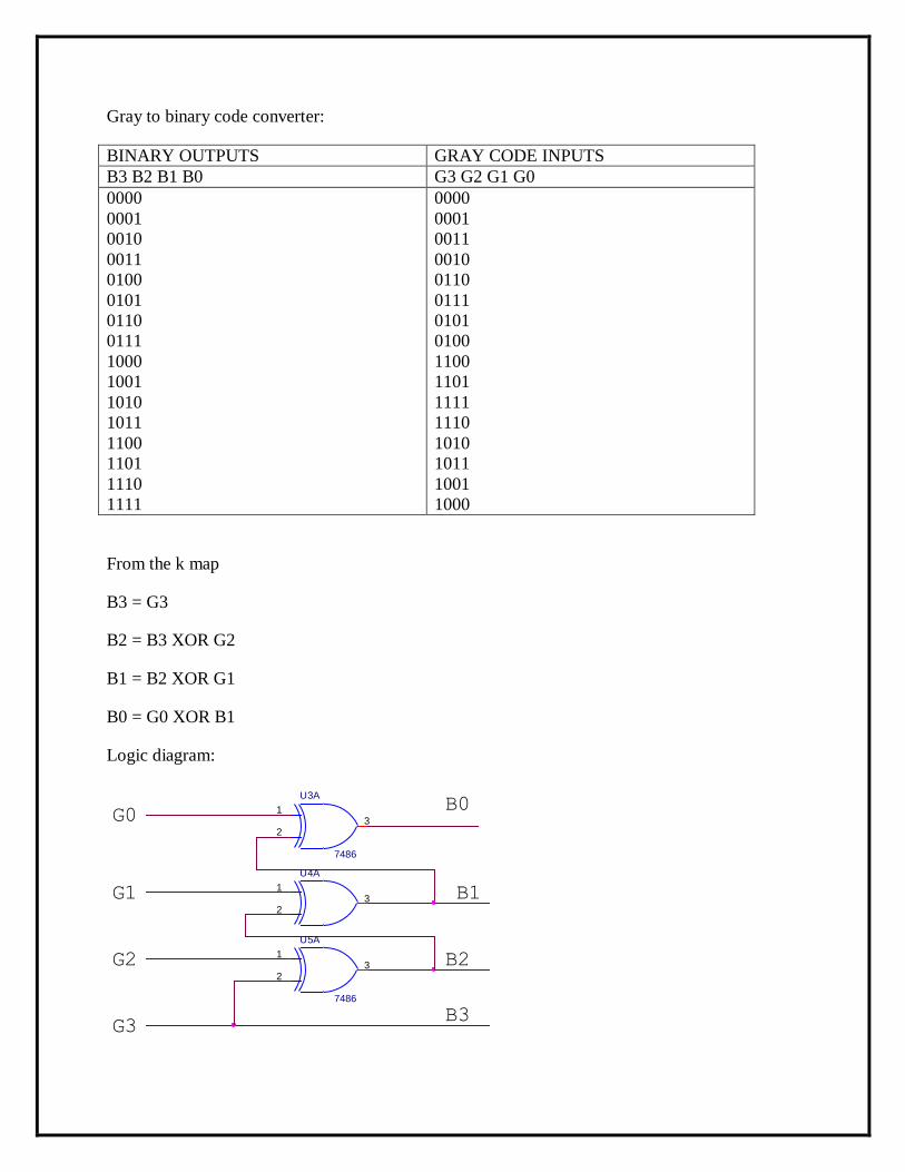
Gray to binary code converter:
BINARY OUTPUTS GRAY CODE INPUTS
B3 B2 B1 B0 G3 G2 G1 G0
0000
0001
0010
0011
0100
0101
0110
0111
1000
1001
1010
1011
1100
1101
1110
1111
0000
0001
0011
0010
0110
0111
0101
0100
1100
1101
1111
1110
1010
1011
1001
1000
From the k map
B3 = G3
B2 = B3 XOR G2
B1 = B2 XOR G1
B0 = G0 XOR B1
Logic diagram:
G2
G3
B0
B3
B1
B2
U3A
7486
1
23
G1
U4A
1
23
G0
U5A
7486
1
23
UNIT III
SYNCHRONOUS SEQUENTIAL CIRCUITS
Sequential circuits:
Combinational logic refers to circuits whose output is strictly depended on the present
value of the inputs. As soon as inputs are changed, the information about the previous
inputs is lost, that is, combinational logics circuits have no memory. In many applications,
information regarding input values at a certain instant of time is required at some future time.
Although every digital system is likely to have combinational circuits, most systems encountered
in practice also include memory elements, which require that the system be described in terms of
sequential logic. Circuits whose outputs depends not only on the present input value but also
the past input value are known as sequential logic circuits. The mathematical model of a
sequential circuit is usually referred to as a sequential machine.
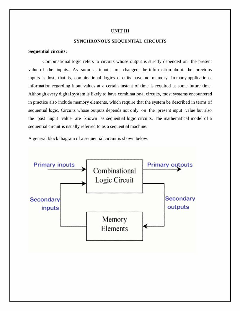
A general block diagram of a sequential circuit is shown below.
The diagram consists of combinational circuit to which memory elements are connected to form
a feedback path. The memory elements are devices capable of storing binary information within
them. The combinational part of the circuit receives two sets of input signals: one is primary
(coming from the circuit environment) and secondary (coming from memory elements). The
particular combination of secondary y input variables at a given time is called the present
state of the circuit. The secondary input variables are also know as the state variables The block
diagram shows that the external outputs in a sequential circuit are a function not only of external
inputs but also of the present state of the memory y elements. The next state of the memory
elements is also a function of external inputs and the present state. Thus a sequential circuit is
specified by a time sequence of inputs, outputs, and internal states.
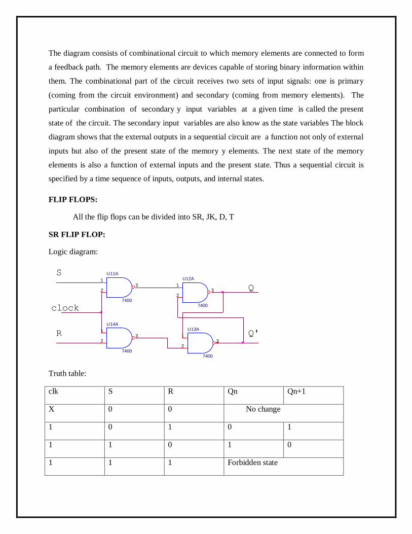
FLIP FLOPS:
All the flip flops can be divided into SR, JK, D, T
SR FLIP FLOP:
Logic diagram:
Truth table:
clk S R Qn Qn+1
X 0 0 No change
1 0 1 0 1
1 1 0 1 0
1 1 1 Forbidden state
Q
U14A
7400
1
23
SU12A
7400
1
23
Q'R
U11A
7400
1
23
U13A
7400
1
23
clock
Characteristics equation:
Qn+1=S+R‟Q
State diagram:
D FLIP FLOP:
The d flip flop has only one input called delay and two outputs Q,Q‟
Logic diagram:
Characteristics equation:
Q(n+1) = D
Truth table:
CLK Input D Output Qn+1
1 0 0
1 1 1
0 X No change
Q
U14A
7400
1
23
U12A
7400
1
23
Q'
U15A
7404
12
U11A
7400
1
23
D
U13A
7400
1
23
clock
State diagram:
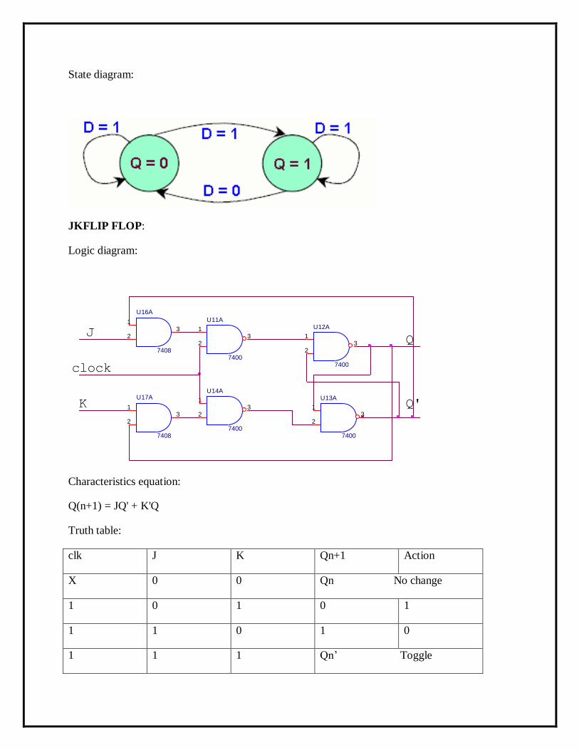
JKFLIP FLOP:
Logic diagram:
Characteristics equation:
Q(n+1) = JQ' + K'Q
Truth table:
clk J K Qn+1 Action
X 0 0 Qn No change
1 0 1 0 1
1 1 0 1 0
1 1 1 Qn‟ Toggle
Q
U17A
7408
1
23
U14A
7400
1
23
J
U16A
7408
1
23 U12A
7400
1
23
Q'K
U11A
7400
1
23
U13A
7400
1
23
clock
State diagram:
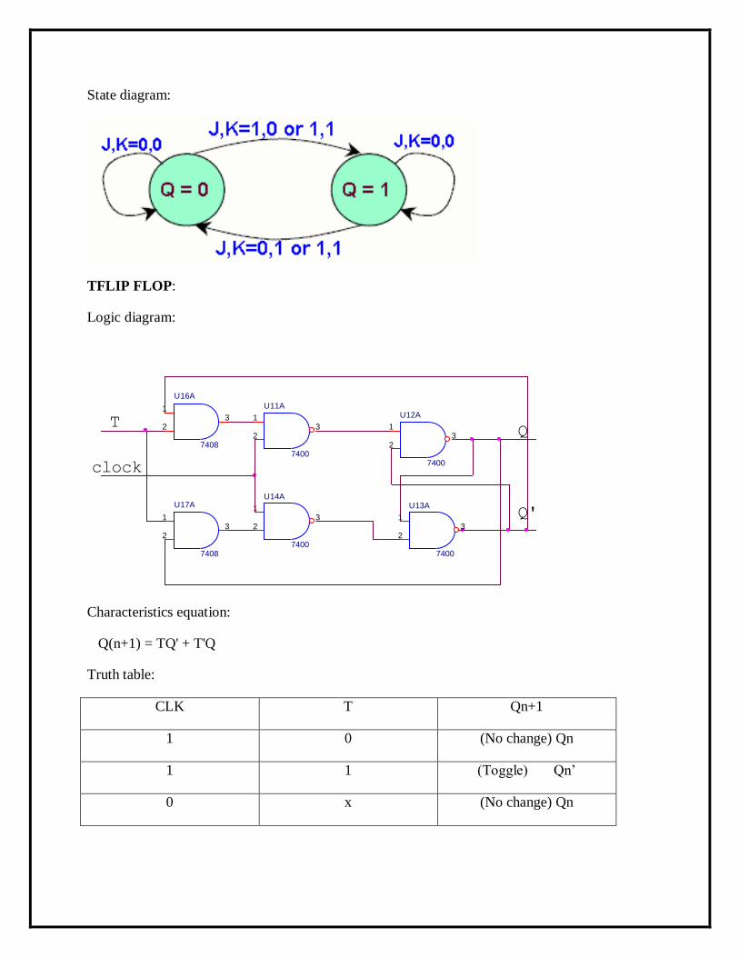
TFLIP FLOP:
Logic diagram:
Characteristics equation:
Q(n+1) = TQ' + T'Q
Truth table:
CLK T Qn+1
1 0 (No change) Qn
1 1 (Toggle) Qn‟
0 x (No change) Qn
QT
U17A
7408
1
23
U14A
7400
1
23
U16A
7408
1
23 U12A
7400
1
23
Q'
U11A
7400
1
23
U13A
7400
1
23
clock
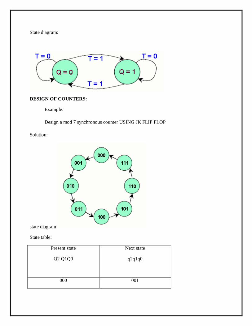
State diagram:
DESIGN OF COUNTERS:
Example:
Design a mod 7 synchronous counter USING JK FLIP FLOP
Solution:
state diagram
State table:
Present state
Q2 Q1Q0
Next state
q2q1q0
000 001
001 010
010 011
011 100
100 101
101 110
110 111
111 000
Excitation table :
PS
Q2 Q1 Q0
NS
Q2 q1 q0
J2 K2 J1 K1 J0 K0
000 001 0 X 0 X 1 X
001 010 0 X 1 X X 1
010 011 0 X X 0 1 X
011 100 1 X X 1 X 1
100 101 X 0 0 X 1 X
101 110 X 0 1 X X 1
110 111 X 0 X 0 1 X
111 000 X 1 X 1 X 1
KARNAUGH MAP:
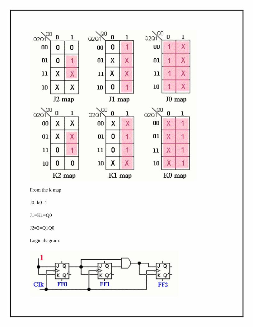
From the k map
J0=k0=1
J1=K1=Q0
J2=2=Q1Q0
Logic diagram:
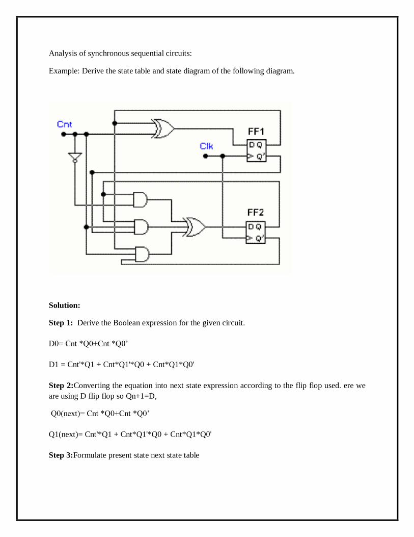
Analysis of synchronous sequential circuits:
Example: Derive the state table and state diagram of the following diagram.
Solution:
Step 1: Derive the Boolean expression for the given circuit.
D0= Cnt *Q0+Cnt *Q0‟
D1 = Cnt'*Q1 + Cnt*Q1'*Q0 + Cnt*Q1*Q0'
Step 2:Converting the equation into next state expression according to the flip flop used. ere we
are using D flip flop so Qn+1=D,
Q0(next)= Cnt *Q0+Cnt *Q0‟
Q1(next)= Cnt'*Q1 + Cnt*Q1'*Q0 + Cnt*Q1*Q0'
Step 3:Formulate present state next state table
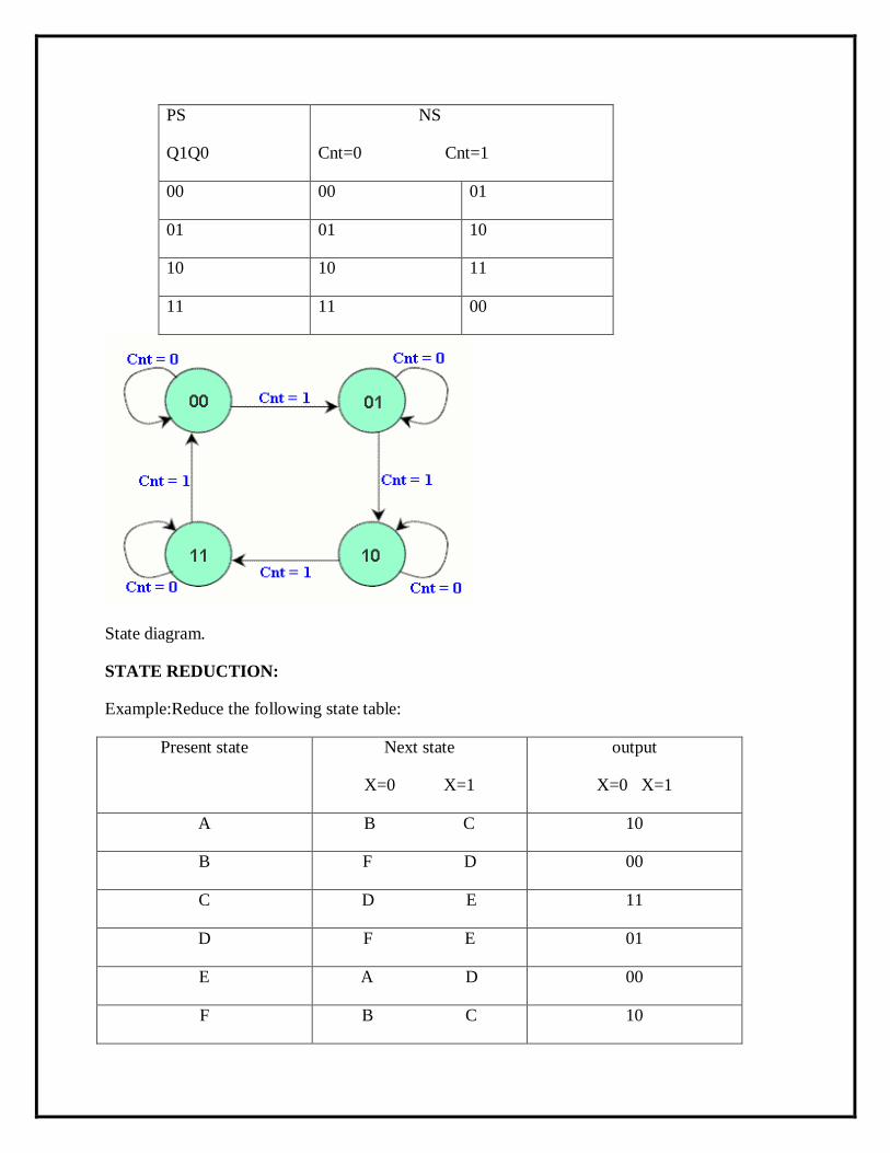
PS
Q1Q0
NS
Cnt=0 Cnt=1
00 00 01
01 01 10
10 10 11
11 11 00
State diagram.
STATE REDUCTION:
Example:Reduce the following state table:
Present state
Next state
X=0 X=1
output
X=0 X=1
A B C 10
B F D 00
C D E 11
D F E 01
E A D 00
F B C 10
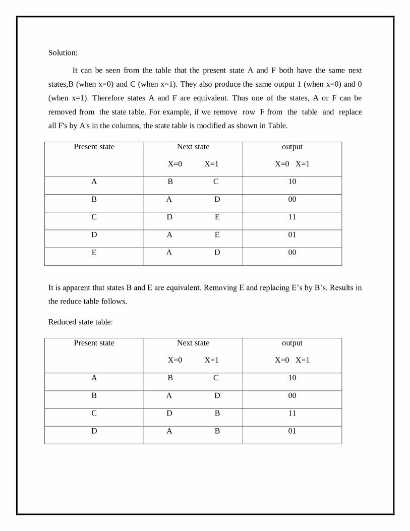
Solution:
It can be seen from the table that the present state A and F both have the same next
states,B (when x=0) and C (when x=1). They also produce the same output 1 (when x=0) and 0
(when x=1). Therefore states A and F are equivalent. Thus one of the states, A or F can be
removed from the state table. For example, if we remove row F from the table and replace
all F's by A's in the columns, the state table is modified as shown in Table.
Present state
Next state
X=0 X=1
output
X=0 X=1
A B C 10
B A D 00
C D E 11
D A E 01
E A D 00
It is apparent that states B and E are equivalent. Removing E and replacing E‟s by B‟s. Results in
the reduce table follows.
Reduced state table:
Present state
Next state
X=0 X=1
output
X=0 X=1
A B C 10
B A D 00
C D B 11
D A B 01
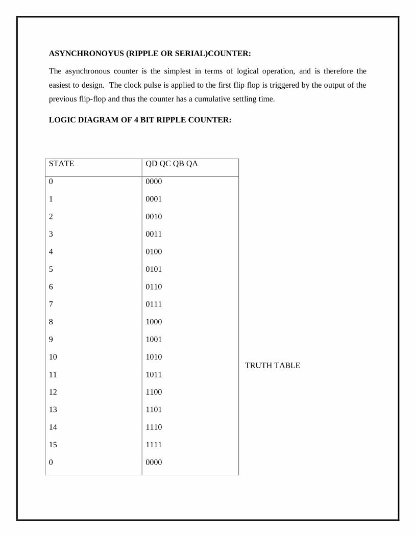
ASYNCHRONOYUS (RIPPLE OR SERIAL)COUNTER:
The asynchronous counter is the simplest in terms of logical operation, and is therefore the
easiest to design. The clock pulse is applied to the first flip flop is triggered by the output of the
previous flip-flop and thus the counter has a cumulative settling time.
LOGIC DIAGRAM OF 4 BIT RIPPLE COUNTER:
TRUTH TABLE
STATE QD QC QB QA
0
1
2
3
4
5
6
7
8
9
10
11
12
13
14
15
0
0000
0001
0010
0011
0100
0101
0110
0111
1000
1001
1010
1011
1100
1101
1110
1111
0000
Mod-number or modulus:
The above counter has 16 different states. Thus, it is a MOD-16 ripple counter. The
MOD-number of a counter is the total number of states it sequences through in each complete
cycle.
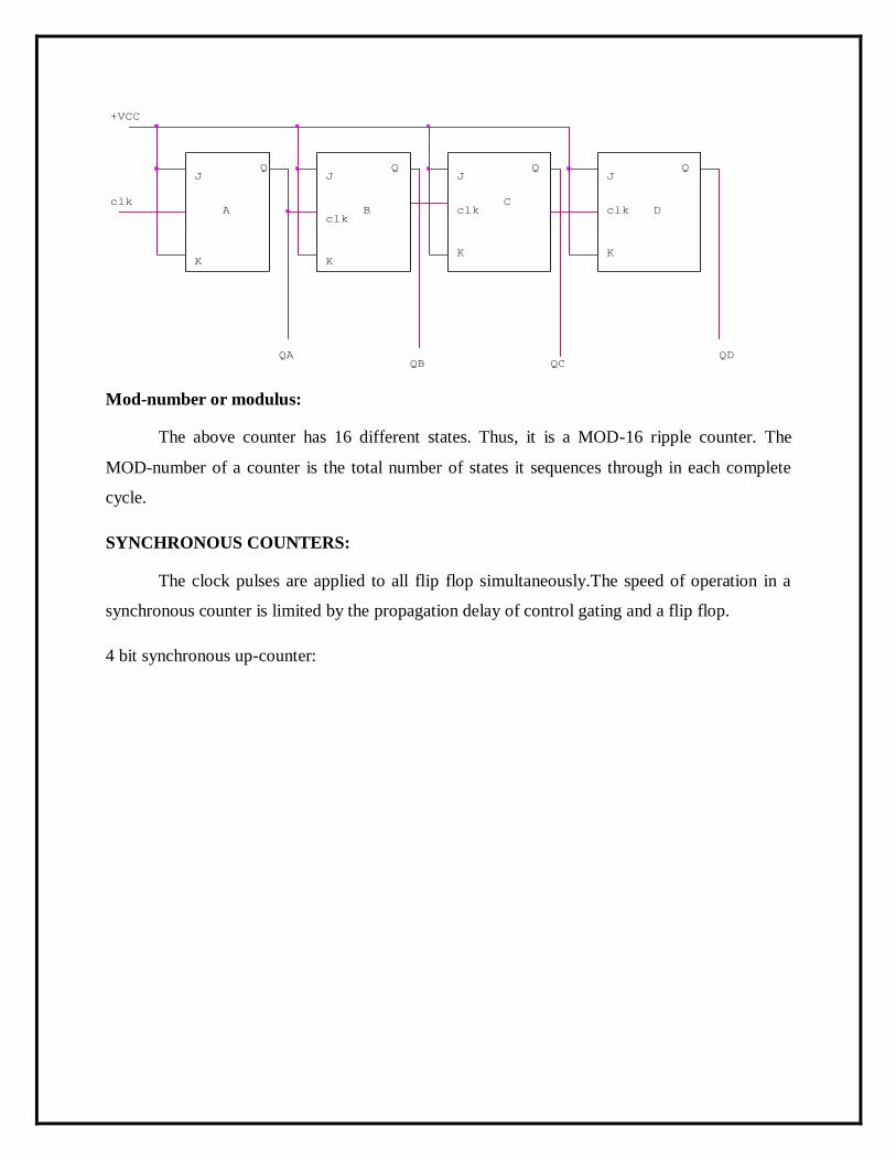
SYNCHRONOUS COUNTERS:
The clock pulses are applied to all flip flop simultaneously.The speed of operation in a
synchronous counter is limited by the propagation delay of control gating and a flip flop.
4 bit synchronous up-counter:
Q
QD
K
A
QJJ
+VCC
J
B clk
K
J
QB
D
QC
Q
C
clk
K
clk
Q
clk
K
QA
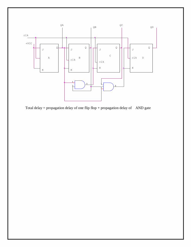
Total delay = propagation delay of one flip flop + propagation delay of AND gate
QB
Q
K
A
QJJ
+VCC
J
B
clk
K
J
1
23
QA
D
QD
Q
C
clk
K
clk
Q
clk
K
QC
1
23
UNIT IV
ASYNCHRONOUS SEQUENTIAL CIRCUITS
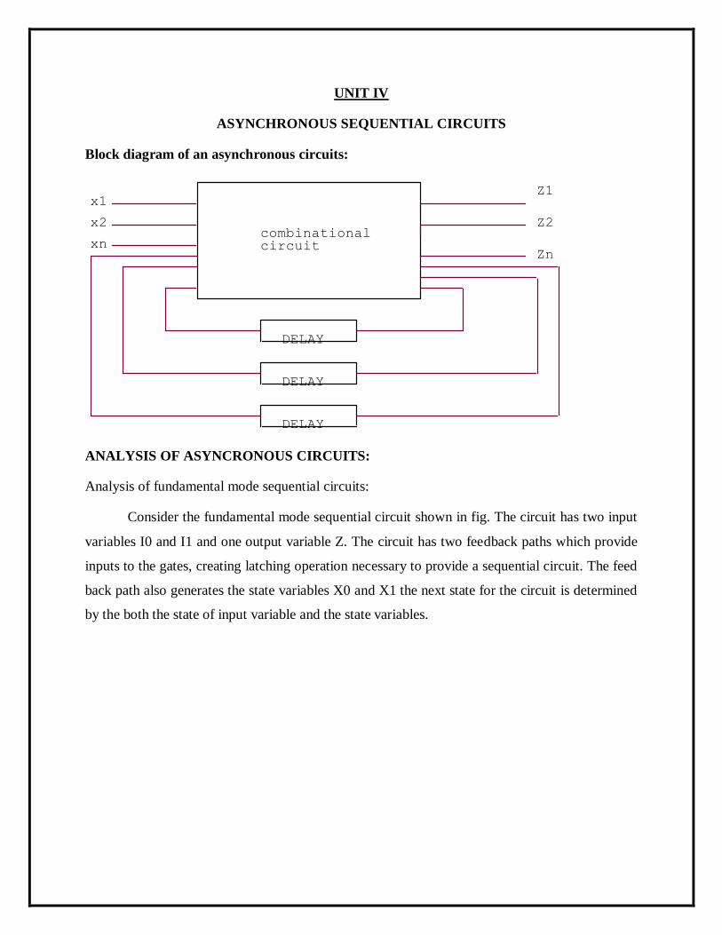
Block diagram of an asynchronous circuits:
ANALYSIS OF ASYNCRONOUS CIRCUITS:
Analysis of fundamental mode sequential circuits:
Consider the fundamental mode sequential circuit shown in fig. The circuit has two input
variables I0 and I1 and one output variable Z. The circuit has two feedback paths which provide
inputs to the gates, creating latching operation necessary to provide a sequential circuit. The feed
back path also generates the state variables X0 and X1 the next state for the circuit is determined
by the both the state of input variable and the state variables.
combinationalcircuit
DELAY
x2 Z2
Z1
Zn
DELAY
xn
DELAY
x1
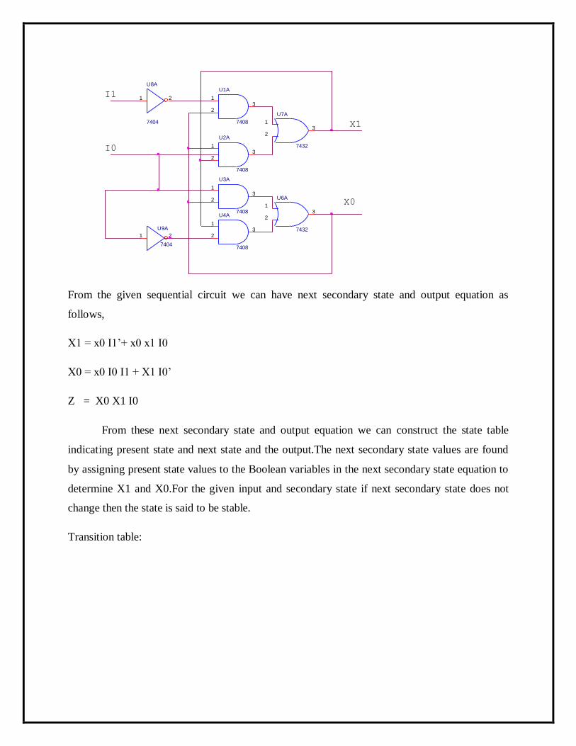
From the given sequential circuit we can have next secondary state and output equation as
follows,
X1 = x0 I1‟+ x0 x1 I0
X0 = x0 I0 I1 + X1 I0‟
Z = X0 X1 I0
From these next secondary state and output equation we can construct the state table
indicating present state and next state and the output.The next secondary state values are found
by assigning present state values to the Boolean variables in the next secondary state equation to
determine X1 and X0.For the given input and secondary state if next secondary state does not
change then the state is said to be stable.
Transition table:
U7A
7432
1
23
U3A
7408
1
23
U4A
7408
1
23
U8A
7404
1 2I1
I0
X1
U1A
7408
1
23
U9A
7404
1 2
U2A
7408
1
23
U6A
7432
1
23
X0
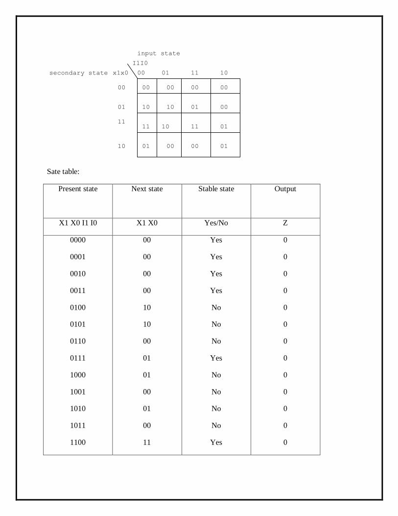
Sate table:
Present state
Next state
Stable state
Output
X1 X0 I1 I0 X1 X0 Yes/No Z
0000
0001
0010
0011
0100
0101
0110
0111
1000
1001
1010
1011
1100
00
00
00
00
10
10
00
01
01
00
01
00
11
Yes
Yes
Yes
Yes
No
No
No
Yes
No
No
No
No
Yes
0
0
0
0
0
0
0
0
0
0
0
0
0
00
input state
01
00
01
11
00
secondary state
11
01
I1I0
00
01
x1x0
00
11
0010
00
00
11
10
10
10
01
00
01
10
1101
1110
1111
10
01
11
No
No
yes
0
1
1
Design of asynchronous sequential circuits:
Design steps:
construction of a primitive flow table from the statement. And intermediate step may include the
development of a state diagram.Primitive flow table is reduced by eliminating redundants states
by using state reduction techniques.state assignment is made the primitive flow table is realized
using appropriate logic elements.
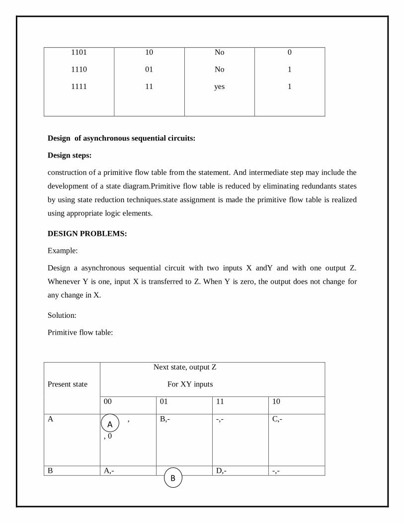
DESIGN PROBLEMS:
Example:
Design a asynchronous sequential circuit with two inputs X andY and with one output Z.
Whenever Y is one, input X is transferred to Z. When Y is zero, the output does not change for
any change in X.
Solution:
Primitive flow table:
Present state
Next state, output Z
For XY inputs
00 01 11 10
A ,
, 0
B,- -,- C,-
B A,- D,- -,-
A
B
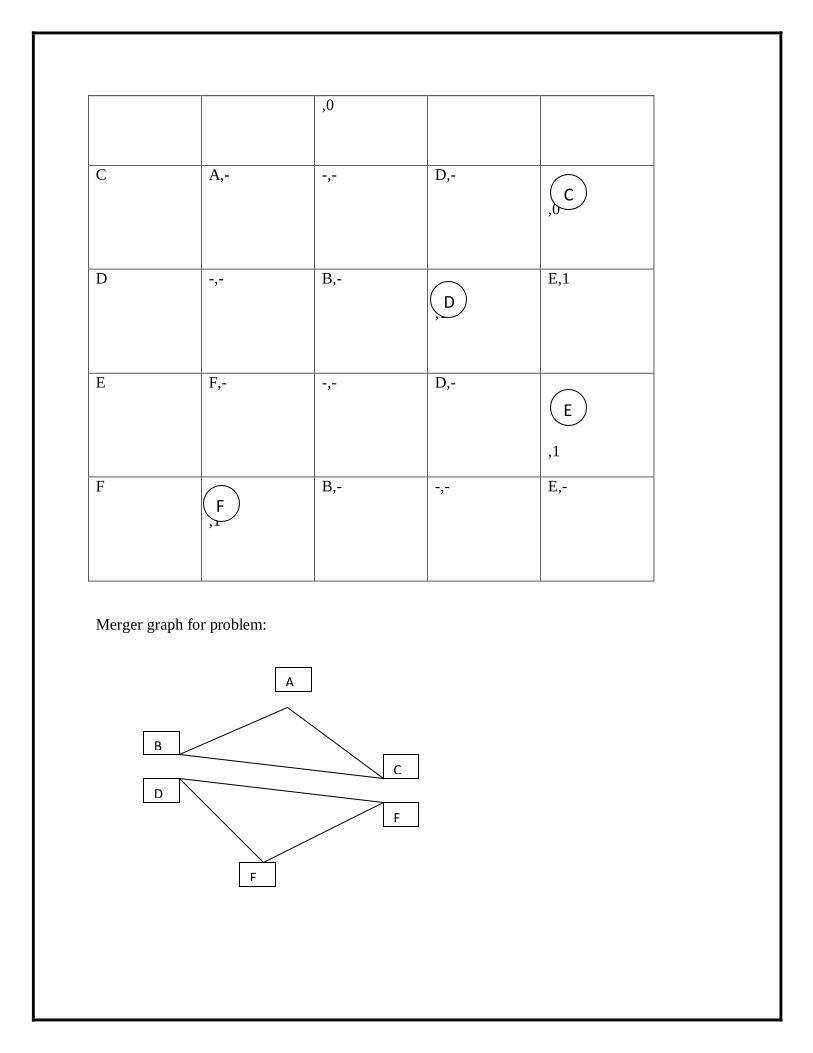
,0
C A,- -,- D,-
,0
D -,- B,-
,1
E,1
E F,- -,- D,-
,1
F
,1
B,- -,- E,-
Merger graph for problem:
C
D
E
F
A
B
C
D
F
E
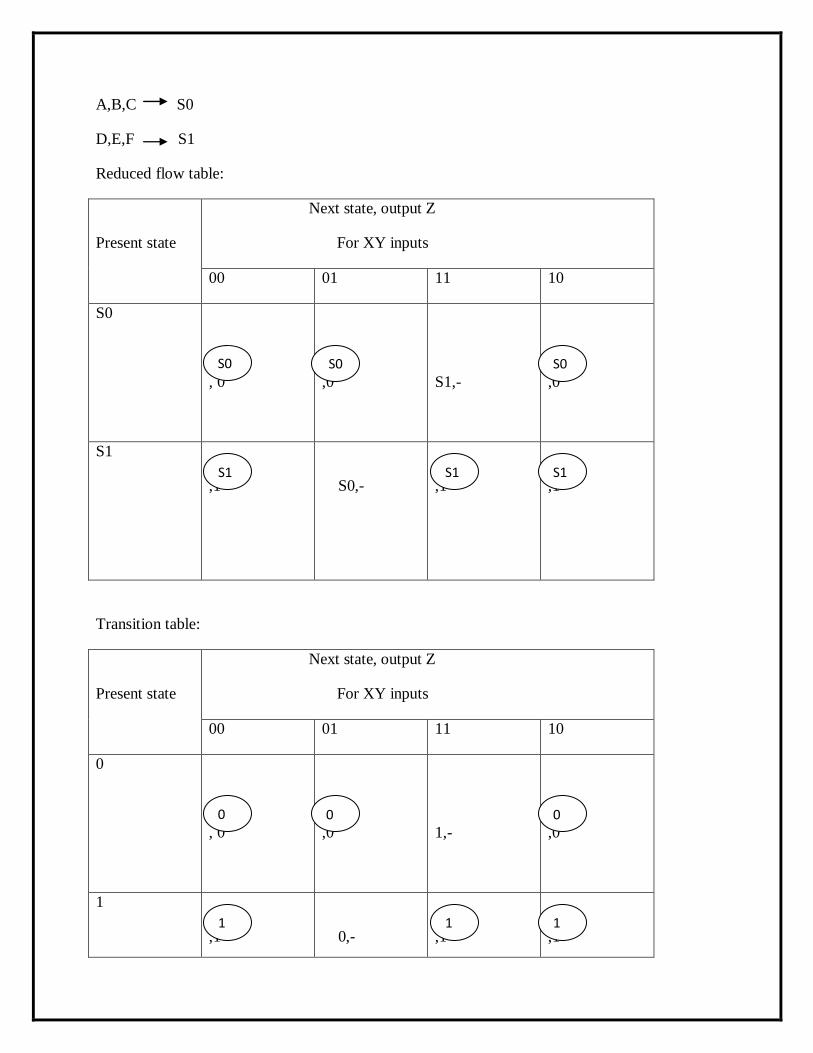
A,B,C S0
D,E,F S1
Reduced flow table:
Present state
Next state, output Z
For XY inputs
00 01 11 10
S0
, 0
,0
S1,-
,0
S1
,1
S0,-
,1
,1
Transition table:
Present state
Next state, output Z
For XY inputs
00 01 11 10
0
, 0
,0
1,-
,0
1
,1
0,-
,1
,1
S0 S0 S0
S1 S1 S1
0 0 0
1 1 1
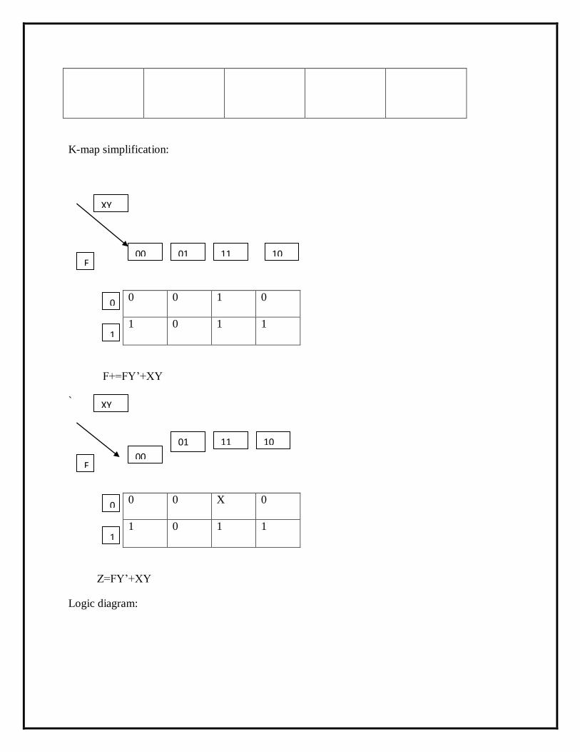
K-map simplification:
0 0 1 0
1 0 1 1
F+=FY‟+XY
`
0 0 X 0
1 0 1 1
Z=FY‟+XY
Logic diagram:
F
XY
0
1
00
F
0
1
00
01 11 10
XY
01 11 10
Example:
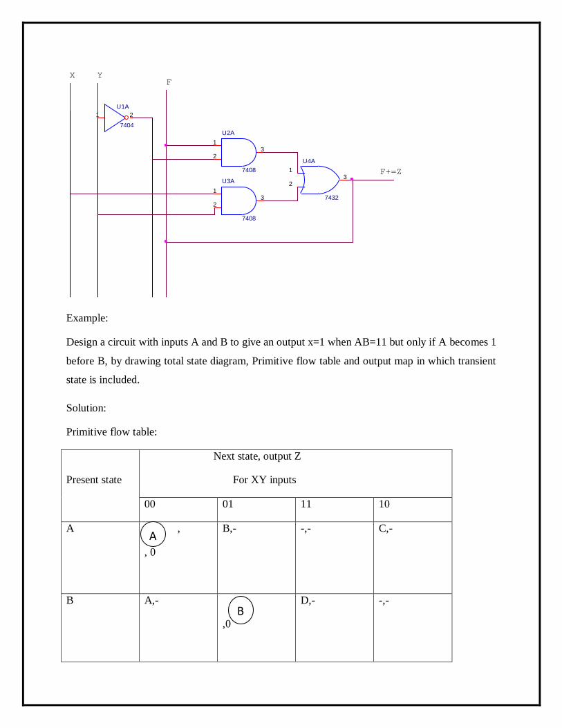
Design a circuit with inputs A and B to give an output x=1 when AB=11 but only if A becomes 1
before B, by drawing total state diagram, Primitive flow table and output map in which transient
state is included.
Solution:
Primitive flow table:
Present state
Next state, output Z
For XY inputs
00 01 11 10
A ,
, 0
B,- -,- C,-
B A,-
,0
D,- -,-
U3A
7408
1
23
Y
U2A
7408
1
23
U1A
7404
1 2
U4A
7432
1
23
FX
F+=Z
A
B
C A,- -,- E,-
,0
D -,- B,-
,0
C,-
E -,- B,-
,1
C,0
State assignment:
A,B,D --- S0
C,E ----S1
Reduced flow table:
Present state
Next state, output Z
For XY inputs
00 01 11 10
S0
, 0
,0
,0
S1,-
S1
S0,-
S0,-
,1
,0
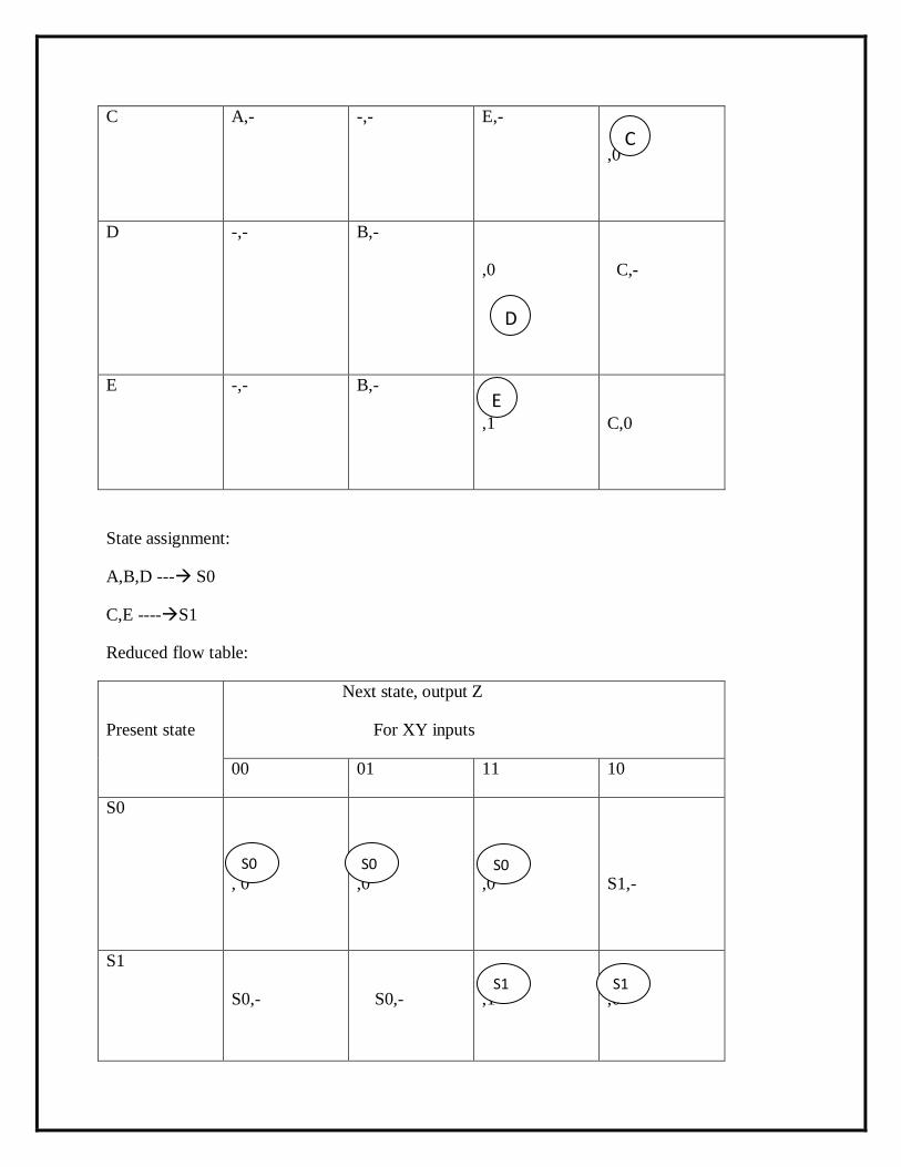
C
D
E
S0 S0
S1 S1
S0
Transition table:
Present state
Next state, output Z
For XY inputs
00 01 11 10
0
, 0
,0
,0
1,-
1
0,-
0,1
,1
,0
K-map:
F+ = F + AB‟
10
AB
0
11
0
00
01
1
F10
00
01
1
0 0
1 1
0
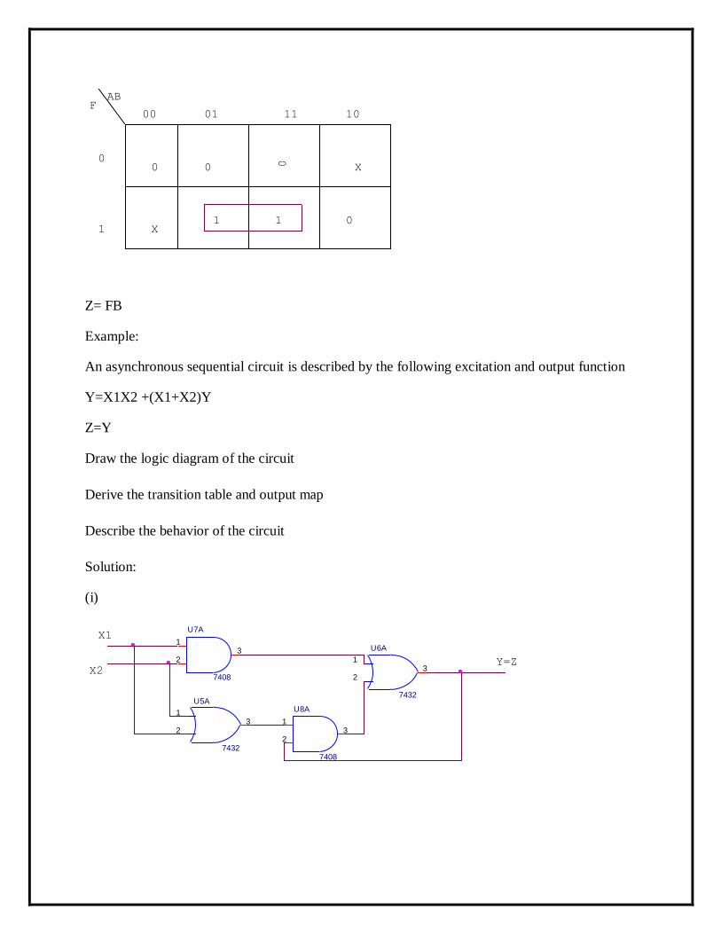
Z= FB
Example:
An asynchronous sequential circuit is described by the following excitation and output function
Y=X1X2 +(X1+X2)Y
Z=Y
Draw the logic diagram of the circuit
Derive the transition table and output map
Describe the behavior of the circuit
Solution:
(i)
X0
AB
X
11
0
00
11
1
F10
00
01
0
X2
U8A
7408
1
23
Y=Z
U7A
7408
1
23
U5A
7432
1
23
X1
U6A
7432
1
23
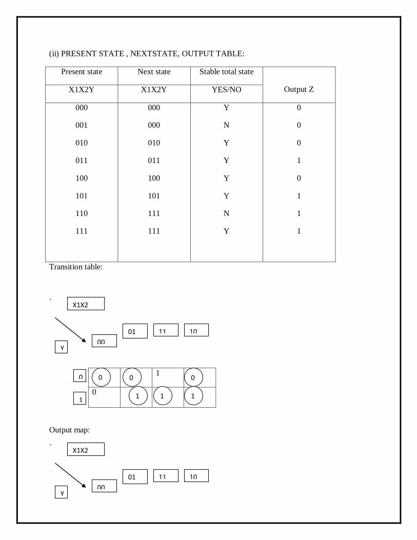
(ii) PRESENT STATE , NEXTSTATE, OUTPUT TABLE:
Present state Next state Stable total state
Output Z X1X2Y X1X2Y YES/NO
000
001
010
011
100
101
110
111
000
000
010
011
100
101
111
111
Y
N
Y
Y
Y
Y
N
Y
0
0
0
1
0
1
1
1
Transition table:
`
1 0
0
Output map:
`
Y
0
1
00
X1X2
01 11 10
0 0 0
1 1 1
Y 00
X1X2
01 11 10
0 0 - 0
- 1 1 1
(iii) The circuit gives carry output of the full adder circuit.
PROGRAMMABLE LOGICDEVICES, MEMORY ANDLOGIC FAMILIES
INTRODUCTION:
Memories are made up of registers. Each registers in the memory is one storage location.
Each location is identified by an adder. Generally the total number of bits that a memory can
store is its capacity.Each register consists of storage elements, each of which stores one-bit
information. A storage element is called a cell.The data stored in a memory by a process called
and are retrieved from the memory by a process called reading.
Classification of memories:
ROM----- MASKED ROM.PROM, EPROM, EEPROM
RAM---- STATIC RAM DYNAMIC RAM
ROM ORGANIZATION:
It is a read only memory. We can read data from the memory we cannot write the data in
the memory. Ie.. it can hold data even if power is turned off. Genally ROM is used to store the
binary codes for the sequence of instruction you want the computer carry out and data as look up
tables. The block diagram of ROM memory is shown in fig. It consists of n address lines and m
output lines. Each bit combination of the address variable is called an address. Each bit
combination that comes out of the output lines is called a data word. Hence, the number of bits
per word is equal to the number of output lines, m; an address is essentially a binary number that
denotes one of the 2n memory location. An output word can be selected by a unique address;
since there is 2n distinct address in a ROM; there are 2n distinct words that are said to be stored
in the unit.
0
1
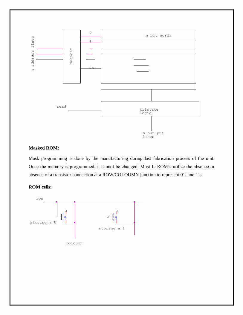
Masked ROM:
Mask programming is done by the manufacturing during last fabrication process of the unit.
Once the memory is programmed, it cannot be changed. Most Ic ROM‟s utilize the absence or
absence of a transistor connection at a ROW/COLOUMN junction to represent 0„s and 1‟s.
ROM cells:
1
tristatelogic
read
decoder
m bit words
2n
n address lines
0
m out putlines
coloumn
row
storing a 1
storing a 0

PROM (programmable ROM)
The PROM can be programmed electrically by the users but cannot be reprogrammed. In
a PROM chip, the manufacturer includes a connection at every intersection of the grid of address
and data lines. PROM‟s are widely used in the control of electrical equipment such as washing
machines and electric ovens.
Fuse technology used in PROM:
Metal links - Nichrom material sufficient amount of current through it
silicon links- narrow strips pf polycrystalline silicon-20 to 30 mA current.
P-N junction.
EPROM ( ERASABLE PROGRAMMABLE READ ONLY MEMORY)
Erasable programmable ROM‟s use MOS circutary.They store 1‟s and 0‟s as a packet of
charge in a buried layer of the Ic chip. EPROM‟s can be programmed by the user with a special
EPROM programmer.
The important point is that we can erase the stored data in the EPROM‟s by exposing the chip
to ultraviolet light through it‟s quartz window for 15 to 20 minutes. It is not possible to erase the
selected data when erased the entire information is lost. The chip can be reprogrammed.
EPROM programming:
When erased each cell in the EPROM contains 1 data is introduced by selectively
programming 0‟s will be programmed, both 1‟s and 0‟s can be presented in the data.
EEPROM (Electrically erasable programmable read only memory)
OR
EAPROM (Electrically Alterable programmable read only memory)
EEPROM also use the MOS circuitry very similar to that of EPROM. Data is stored as charge
or no charge on an insulated layer or insulated floating gate in the device. The insulating layer is
made very thin (<200 A). Therefore a voltage as low as 20 to 25 V can be used to move charges
across the thin barrier in either direction for programming or erasing. EEPROM allows selective
erasing at the register levels rather than erasing all data.
PROGRAMMABLE LOGIC DEVICES:
Various combinational and sequential circuits are designed using logic gates and flip
flops. To implement such combinational and sequential circuits , the designer has to interconnect
several SSI and MSI chips by making connections to the IC packages.
Logic circuit can also be designed using Programmable logic device (PLD) that have all the
gates necessary for a logic circuit design in a single package. In such devices, there are
provisions to perform the interconnections of the gates internally so that the desired logic can be
implemented.
There are two types of PLD
Programmable Array logic (PAL) (fixed AND , programmable OR)
Programmable Logic Array (PLA) (fixed OR , programmable AND)
Programmable Logic Array (PLA):
PLA is a type of fixed architecture logic devices with programmable AND gates followed by
programmable OR gates. The PLA is used to implement a complex combinational circuit.
A PLA is similar to a ROM in concept except that it does not provide full decoding of the
variables and does not generate all the minterms as in the ROM. Thus, in a PLA, the decoder is
replaced by a group of AND gates, each of which can be programmed to produce a product
(AND) terms of the input variables. The AND and OR gates inside the PLA are initially
fabricated with fuses among them. The specific Boolean functions are implemented in SOP form
by blowing appropriate fuses and leaving the desired connection. It is similar to reprogramming
of ROM‟s.For this reason logic array is called a programmable logic array.
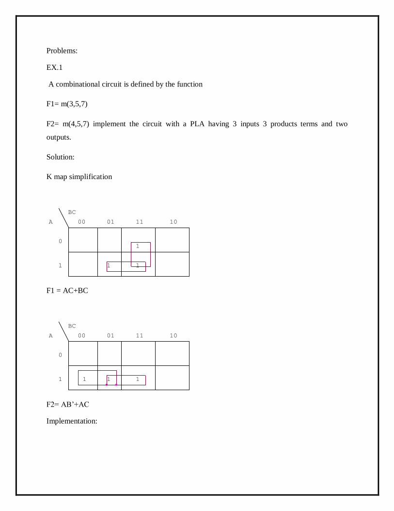
Problems:
EX.1
A combinational circuit is defined by the function
F1= m(3,5,7)
F2= m(4,5,7) implement the circuit with a PLA having 3 inputs 3 products terms and two
outputs.
Solution:
K map simplification
F1 = AC+BC
F2= AB‟+AC
Implementation:
0
1
01 10
1
1
1100
1
A
BC
0
1
01 10
1 1
1100
1
A
BC
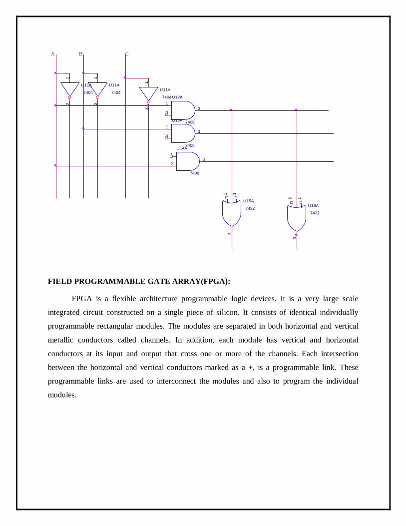
FIELD PROGRAMMABLE GATE ARRAY(FPGA):
FPGA is a flexible architecture programmable logic devices. It is a very large scale
integrated circuit constructed on a single piece of silicon. It consists of identical individually
programmable rectangular modules. The modules are separated in both horizontal and vertical
metallic conductors called channels. In addition, each module has vertical and horizontal
conductors at its input and output that cross one or more of the channels. Each intersection
between the horizontal and vertical conductors marked as a +, is a programmable link. These
programmable links are used to interconnect the modules and also to program the individual
modules.
U11A
74041
2
C
U11A
7404
12
U16A
7432
123
U13A
7408
1
23
A
U11A
7404
12
U14A
7408
1
23
B
U12A
7408
1
23
U15A
7432
123
UNIT V
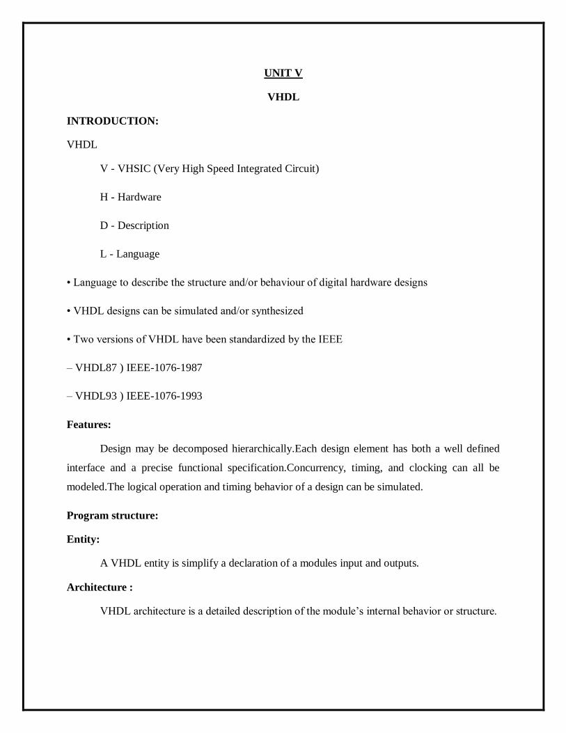
VHDL
INTRODUCTION:
VHDL
V - VHSIC (Very High Speed Integrated Circuit)
H - Hardware
D - Description
L - Language
• Language to describe the structure and/or behaviour of digital hardware designs
• VHDL designs can be simulated and/or synthesized
• Two versions of VHDL have been standardized by the IEEE
– VHDL87 ) IEEE-1076-1987
– VHDL93 ) IEEE-1076-1993
Features:
Design may be decomposed hierarchically.Each design element has both a well defined
interface and a precise functional specification.Concurrency, timing, and clocking can all be
modeled.The logical operation and timing behavior of a design can be simulated.
Program structure:
Entity:
A VHDL entity is simplify a declaration of a modules input and outputs.
Architecture :
VHDL architecture is a detailed description of the module‟s internal behavior or structure.
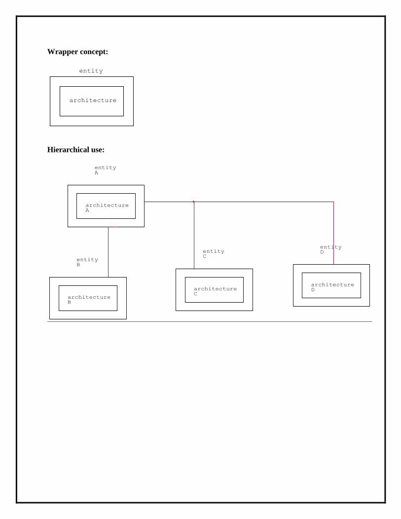
Wrapper concept:
Hierarchical use:
entityC
entityB
architectureB
entityA
architectureA
architectureD
entityD
architectureC
entity
architecture
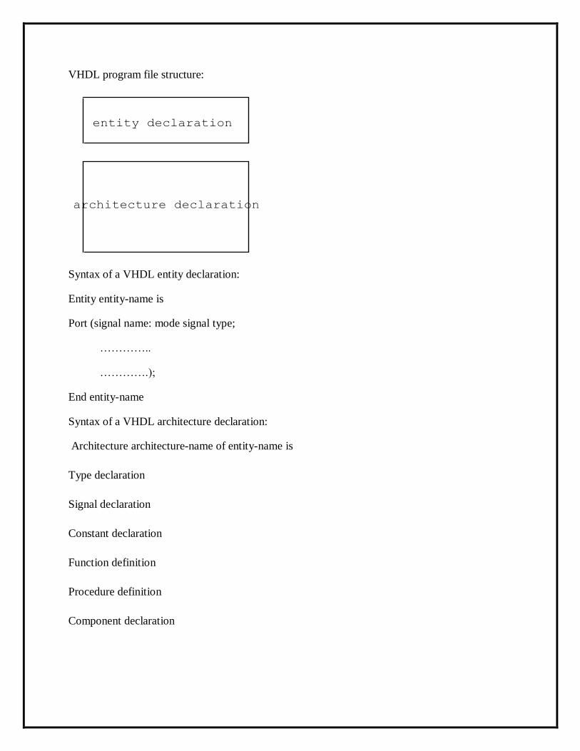
VHDL program file structure:
Syntax of a VHDL entity declaration:
Entity entity-name is
Port (signal name: mode signal type;
…………..
………….);
End entity-name
Syntax of a VHDL architecture declaration:
Architecture architecture-name of entity-name is
Type declaration
Signal declaration
Constant declaration
Function definition
Procedure definition
Component declaration
entity declaration
architecture declaration

Begin
Concurrent statement
End architecture-name;
TYPES, CONSTANTS, ARRAYS:
Vhdl predefined types:
bit character Severity level
bit_vector integer string
boolean real time
Predefined operators for VHDL‟s integer and Boolean types:]
Integer operators:
+
-
*
/
mod
rem
abs
**
Addition
Subtraction
Multiplication
Division
Modulo division
Modulo remainder
Absolute value
exponential
Boolean operators:
and
or
nand
nor
xor
xnor
not
AND
OR
NAND
NOR
EXCLUSIVE OR
EXCLUSIVENOR
COMPLEMENTATION
Syntax of VHDL types and constant declaration:
type type_name is (value list):
subtype subtype_name is type_name start to end;
subtype subtype_name is type_name start down to end;
constant constant_name: type name := value;
syntax of VHDL array declaration:
type type-name is array (start to end ) of element-type;
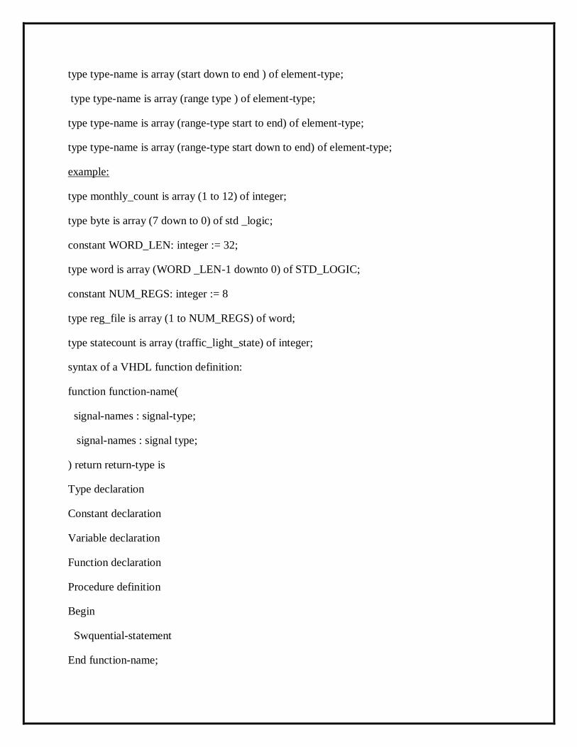
type type-name is array (start down to end ) of element-type;
type type-name is array (range type ) of element-type;
type type-name is array (range-type start to end) of element-type;
type type-name is array (range-type start down to end) of element-type;
example:
type monthly_count is array (1 to 12) of integer;
type byte is array (7 down to 0) of std _logic;
constant WORD_LEN: integer := 32;
type word is array (WORD _LEN-1 downto 0) of STD_LOGIC;
constant NUM_REGS: integer := 8
type reg_file is array (1 to NUM_REGS) of word;
type statecount is array (traffic_light_state) of integer;
syntax of a VHDL function definition:
function function-name(
signal-names : signal-type;
signal-names : signal type;
) return return-type is
Type declaration
Constant declaration
Variable declaration
Function declaration
Procedure definition
Begin
Swquential-statement
End function-name;
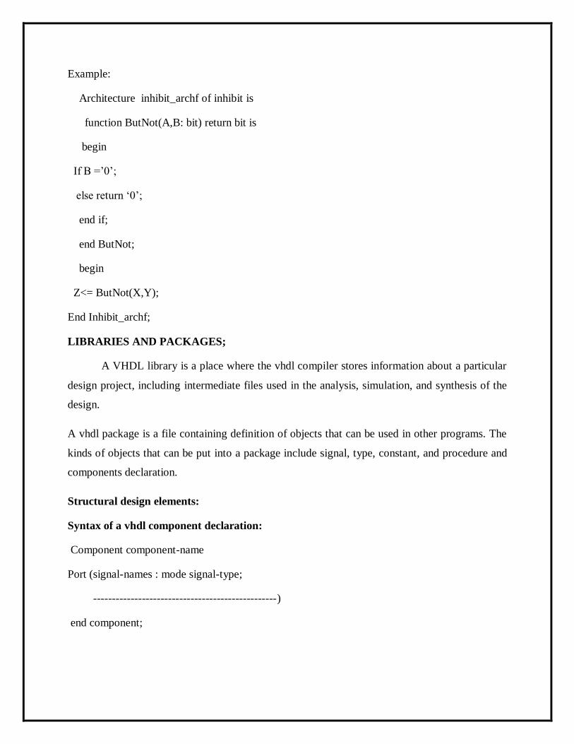
Example:
Architecture inhibit_archf of inhibit is
function ButNot(A,B: bit) return bit is
begin
If B =‟0‟;
else return „0‟;
end if;
end ButNot;
begin
Z<= ButNot(X,Y);
End Inhibit_archf;
LIBRARIES AND PACKAGES;
A VHDL library is a place where the vhdl compiler stores information about a particular
design project, including intermediate files used in the analysis, simulation, and synthesis of the
design.
A vhdl package is a file containing definition of objects that can be used in other programs. The
kinds of objects that can be put into a package include signal, type, constant, and procedure and
components declaration.
Structural design elements:
Syntax of a vhdl component declaration:
Component component-name
Port (signal-names : mode signal-type;
-------------------------------------------------)
end component;
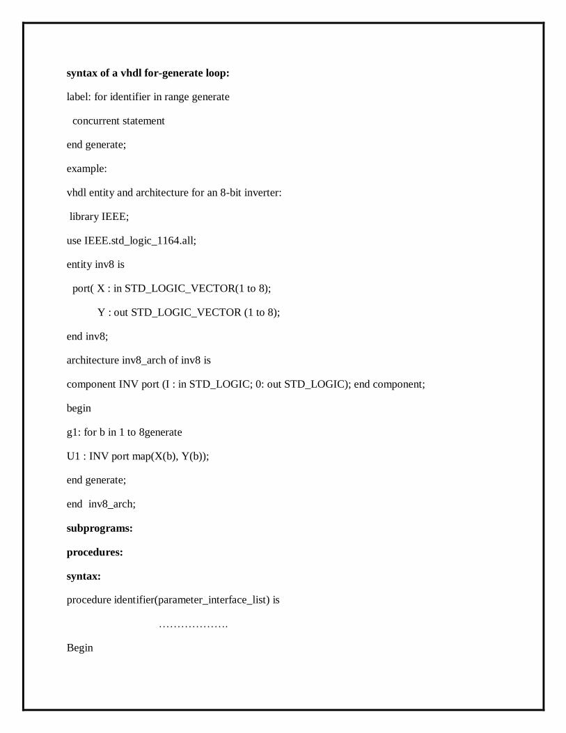
syntax of a vhdl for-generate loop:
label: for identifier in range generate
concurrent statement
end generate;
example:
vhdl entity and architecture for an 8-bit inverter:
library IEEE;
use IEEE.std_logic_1164.all;
entity inv8 is
port( X : in STD_LOGIC_VECTOR(1 to 8);
Y : out STD_LOGIC_VECTOR (1 to 8);
end inv8;
architecture inv8_arch of inv8 is
component INV port (I : in STD_LOGIC; 0: out STD_LOGIC); end component;
begin
g1: for b in 1 to 8generate
U1 : INV port map(X(b), Y(b));
end generate;
end inv8_arch;
subprograms:
procedures:
syntax:
procedure identifier(parameter_interface_list) is
……………….
Begin
…………
end
return statement in procedure:
syntax:
return_statement (label:) return;
procedure parameters:
interface list
syntax
constant / variable/signal
identifier {………….}: [mode] subtype_indication [:= static_expression]
mode…..> in /out/inout.
Call statements:
Ex.
Callprocess:p(s1,s2,val1);
Callprocess:process is
Begin
P(s1,s2,val);
Wait on s1,s2;
End process call_process.
Functions:
Syntax:‟
Function identifier
[…………..] return type_mark is
……………..
Begin
……………
End
Data flow design elements:
Several additional concurrent statements allow vhdl to describe a circuit in terms of the flow of
data and operations on it within the circuit. This style is called a data flow description or
dataflow design.
Syntax :
Signal-name <= expression;
Signal-name <= expression when Boolean-expression else
………………………………………………..
expression;
behavioral design elements:
Behavioral design or behavioral description is one of the key benefits of hardware description
language in general and VHDL in particular.
Syntax of a VHDL if statement:
If Boolean expression then sequential-statements
end if;
if Boolean-expression then sequential statement
else sequential-statements
end if;
………………..
………………..
end if;
Syntax of a VHDL loop statement:
Loop
Sequential-statement
……………..
……….
End loop;
Syntax of a VHDL for loop statement:
for identifier in range loop
Sequential-statement
…………………….
End loop;
SEQUENTIAL CIRCUIT DESIGN WITH VHDL
Clocked circuits:
Ex.
Behavioural modeling for a positive edge triggered d flip flop:
Library ieee;
Use ieee.std_logic_1164.all;
Entity vposdff is
Port( clk,clr,d : in STD_Logic;
Q : out std_logic);
End vposdff;
Architecture vposdff_arch of vpodff is
Begin
Process (clk,clr)
Begin
If clr =‟1‟ then q <= „1‟ then q <= d;
End if;
End process;
End vposdff_arch.
TEST BENCHES:
A test bench specifies a sequence of inputs to be applied by the simulator to an HDL-
based design, such as a VHDL entity. The entity being tested is often called the unit under test
(UUT).
VHDL programs:
8 bit adder:
Library IEEE;
Use IEEE.std_logic_1164.all;
Use IEEE.std_logic_arith.all;
Entity vadd is
port(
A,B : in UNSIGNED (7 down to 0);
C : in SIGNED (7 down to 0);
D : in STD_LOGIC_VECTOR (7 down to 0);
S :out UNSIGNED (8 down to 0);
T : out SIGNED (8 down to 0);
U : out SIGNED (7 down to 0);
V : out STD_LOGIC_VECTOR (8 down to 0)
);
End vadd;
Architecture vadd_arch of vadd is
Begin
S<= („0‟& A) + („0‟ & B);
T <= A+C;
U <= C + SIGNED (D);
V <= C – UNSIGNED (D);
End vadd_arch;
Full adder:
Library IEEE;
Use ieee.std_logic_1164.all;
Entity fulladder is
Port (A,B,Cin : in std_logic ;
Sum,carry : out std_logic);
End fulladder;
Architecture adder_arch of full adder is
Begin
Sum<= A xor B xor Cin;
Carry <= (A and B) or (B and Cin) or (Cin and A);
End;
4:1 multiplexer:
Library ieee;
Use ieee.std_logic_1164.all;
Entity mux is
Port(s1,s0,d0,d1,d2,d3: in std _logic;
Y : out std_logic );
End mux;
Architecture arch_mux of mux is
Begin
Y <= ((not S1) and (not s0) and d0) or ((not s1) and s0 and d1) or (s1 and (not s0)and d2 or (s1
and s0 and d3);
End arch_mux;
1:4 demultiplexer:
Library ieee;
Use ieee.std_logic_1164.all;
Entity demux is
Port(d,s1,s0: in std_logic;
Y0,y1,y2,y3: out std_logic);
End demux;
Architecture demux_arch of demux is
Begin
y0 <= d and (not s1) and (not s0);
y1 <= d and (not s1) and (s0);
y2 <= d and (s1) and (not s0);
y3 <= d and (s1) and (s0);
end;
SR flip flop:
Library ieee;
Use ieee.std_logic_1164.all;
Entity srff1 is
Port(s,r : in std_logic; q,nq : inout std_logic);
end srff1;
architecture srff_arch of arff1 is begin
q <= r nor nq;
nq <= s nor q;
end;
clocked SR flip flop:
library ieee;
use ieee.std_logic_1164.all;
entity clksr is
port(s,r,clk : in std_logic;
m,n : inout std_logic;
q,nq: inout std_logic);
ends clksr;
architecture clksr_arch of clksr is
component srff1 is
port(s,r : in std_logic;
q,nq : inout std_logic);
end component;
begin
m<= s and clk;
n <= r and clk;
a1 : srff1 port map(m,n,q,nq);
end;
d flip flop:
library ieee;
use ieee.std_logic_1164 all;
entity dfff1 is
port(d,clk,reset: in std_logic;
q: out std_logic);
end dfff1;
architecture arch_dflipflop of dfff1 is
begin
process (clk)
begin
if (clk‟event and clk =‟1‟) then
if reset =‟0‟ then
q<= „0‟;
else
q<=d;
end if;
end if;
end process;
end;
4-bit asynchronous/ripple counter:
Library ieee;
Use ieee.std_logic_1164.all;
Entity ripple_counter is
Port(vcc,clk,reset : in std_logic;
q,nq: inout std_logic_vector (0 to 3));
end ripple_counter;
architecture arch_ripple_counter of ripple_counter is
component jkff1 is
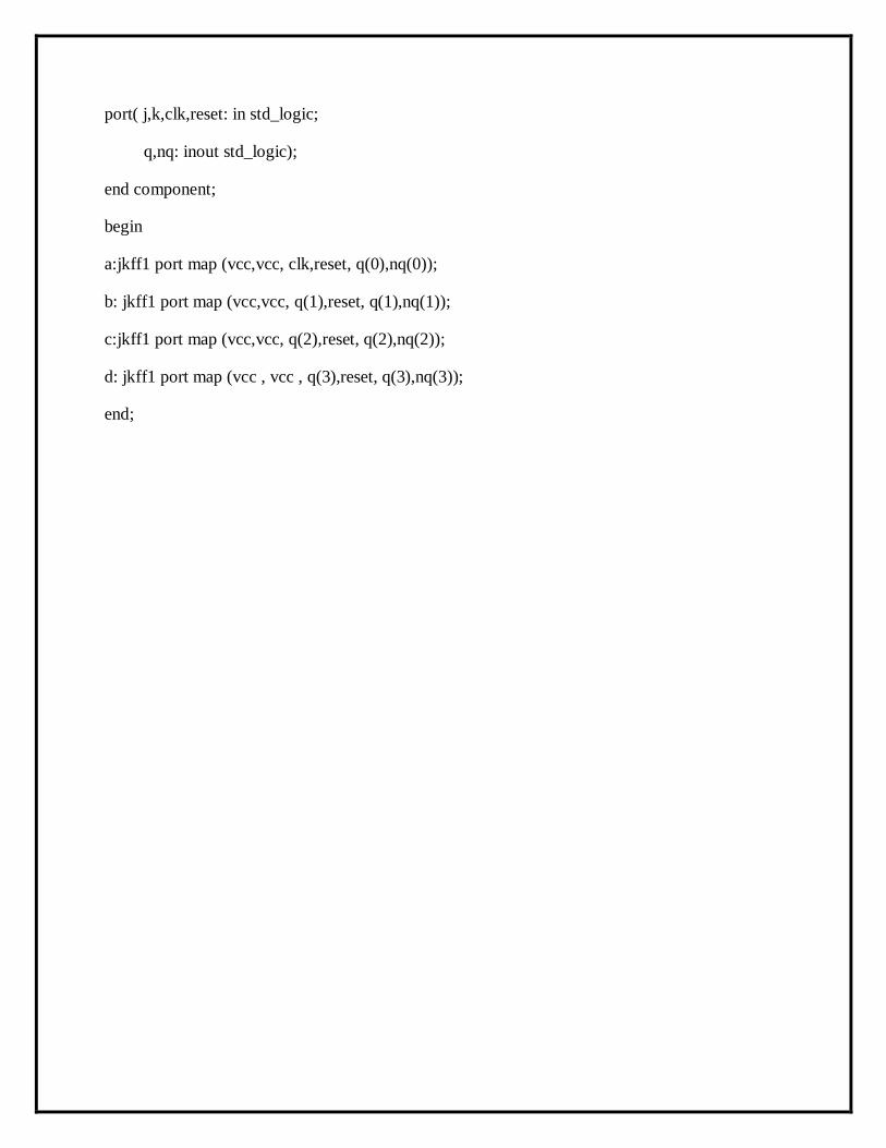
port( j,k,clk,reset: in std_logic;
q,nq: inout std_logic);
end component;
begin
a:jkff1 port map (vcc,vcc, clk,reset, q(0),nq(0));
b: jkff1 port map (vcc,vcc, q(1),reset, q(1),nq(1));
c:jkff1 port map (vcc,vcc, q(2),reset, q(2),nq(2));
d: jkff1 port map (vcc , vcc , q(3),reset, q(3),nq(3));
end;