correlation analysis of tem images of nanocrystal molecules
TRANSCRIPT

1
Correlation Analysis of TEM Images of Nanocrystal
Molecules
C.M. Micheela, D. Zanchetb, A. Paul Alivisatos*
Department of Chemistry, University of California, Berkeley and Materials Science Division,
Lawrence Berkeley National Laboratory, Berkeley, CA 94720
RECEIVED DATE (to be automatically inserted after your manuscript is accepted if required
according to the journal that you are submitting your paper to)
* Corresponding author. Email: [email protected]. a: present address: IBM Almaden Research
Center, San Jose, CA 95120, [email protected], b: present address: Brazilian Synchrotron Light
Laboratory-LNLS, Campinas, SP, Brazil, [email protected].
ABSTRACT
Quantitative characterization of images of nanocrystals and nanostructures is a challenging but
important task. The development and optimization of methods for the construction of complex
nanostructures rely on imaging techniques. Computer programs were developed to quantify TEM
images of nanocrystal/DNA nanostructures, and results are presented for heterodimers and trimers of
gold nanocrystals. The programs presented here have also been used to analyze more complex trimers
and tetramers linked by branched DNA, as well as for structures made from attaching gold
nanocrystals to CdSe/ZnS core-shell quantum dots. This work has the additional goal of enabling
2
others to quickly and easily adapt the methods for their own use.
INTRODUCTION
Over the past several years, the ability to fabricate and characterize nanostructures as well as the
ability to apply the unique characteristics of nanocrystals—such as their optical properties and small
sizes—to biological problems have improved dramatically. Biomolecules and nanocrystals are similar
in size, which makes it possible to adapt well-established techniques used for each separately to the
characterization of hybrid structures. For example, gel electrophoresis has been used to purify and
characterize nanocrystal/biomolecule conjugates and nanostructures—so-called nanocrystal
molecules.1-6 Imaging techniques used in both fields include optical microscopy, which has been used
in DNA arrays, single nucleotide polymorphism detection, and cell motility assays.7-9 Atomic force
microscopy (AFM) is used to study nanostructures constructed from gold nanocrystals, proteins, and
DNA.10-12 Transmission electron microscopy (TEM) is an indispensable tool for the verification of a
wide variety of nanostructures.1-4,6
Arguably, imaging techniques such as these are the most important methods of characterizing
nanocrystals and nanocrystal/biomolecule nanostructures. These methods range from simple
photography, used for imaging agarose and polyacrylamide gels, to TEM, used for visualization of
most nanostructures.13 While useful qualitative analysis of such images is often straightforward,
extending the analysis to yield quantitative information is often challenging.1,14 It may be easy to
measure particle size distributions using standard image analysis software, but it is more difficult to
measure interparticle distances or identify groups of nanocrystals, especially if special constraints need
to be followed. This is the focus of the work presented here, which offers solutions to these problems
as well as programs that can be readily adapted for use by others.
The development of the synthesis of discrete gold nanocrystal/DNA nanostructures has taken place
over the last ten years.1,6,15-18 During that time, our ability to characterize the structures using TEM and
image analysis has increased substantially, primarily through refinement of the synthetic methods and

3
subsequent increases in yield. In the initial work, isolated structures could be seen scattered over a
sample grid, mixed in with various impurities.15,16 Later on, it was possible to see fields of structures
in single images.1,6,17,18 This has motivated the work presented in detail in this paper, allowing us to
easily characterize complex structures. The analysis techniques include pair correlation functions
useful for dimers and higher-order structures as well as quantitation of higher order structures. The
programs also allow confirmation of lower-yield structures whose syntheses have not yet been
optimized, since random distribution of nanocrystals on a TEM grid can lead to misleading
interpretation of the results. The use of these programs in the characterization of nanocrystal
molecules is presented below.
EXPERIMENTAL SECTION
Gold nanocrystals, gold/DNA conjugates, dimers and trimers were prepared according to previously
published methods.1,2 The gold nanocrystals (Ted Pella, Redding, CA) are 5 or 10 nm in diameter and
the DNA length varies from 50-100 bases. Briefly, to produce dimers, gold nanocrystals attached to
single DNA oligonucleotides were obtained by mixing the nanocrystals with thiol-modified single-
stranded DNA and purified by electrophoresis. Dimers were then obtained by mixing gold/DNA
conjugates with complementary gold/DNA conjugates, and were further purified using gel
electrophoresis. To prepare samples for TEM, formvar-coated carbon grids (Ted Pella, Redding, CA)
were first prepared with a solution of bacitracin (Sigma-Aldrich, St. Louis, MO) to make the grids
hydrophilic. Five µL of a 500 µg/mL solution of bacitracin was dropped on the grid for 30 s; the
excess was then wicked off with filter paper. Each grid was then washed with a drop of distilled
deionized water for 30 s; the drop was then wicked off. The sample, at approximately 100-500 nM,
was then dropped onto the grid and wicked off after 30 s. Each grid was again washed with a drop of
water for 30 s. The excess was wicked off, and the grids were allowed to dry under cover of a Petri
dish to prevent dust from settling on the grids. Transmission electron microscopy was conducted in an

4
FEI Tecnai 12 microscope at the Electron Microscope Laboratory at UC Berkeley (Berkeley, CA).
The accelerating voltage was 100 kV. Images were collected with a Gatan model 780 dual view
digital camera with resolution of 1300 x1300 pixels. 50-100 images were collected per sample, and
magnification (generally 60,000x) and sample density on the grids were optimized for rapid and
accurate analysis. The magnification was calibrated periodically using a calibration grid; this was
important, as the magnification could be off by several percent.
Computer programs were developed to analyze the TEM data. The images were first analyzed using
Image Pro Plus graphics analysis software (Media Cybernetics, Inc., Bethesda, MD). Nanocrystals
were counted by the program, and lists of nanocrystal locations and diameter were recorded. The
nanocrystal lists were treated using the programs written in LabVIEW (National Instruments, Austin,
TX). These programs are included in the supplementary information and are available at
http://www.cchem.berkeley.edu/pagrp/publications.html.
RESULTS AND DISCUSSION
Program Operation
5
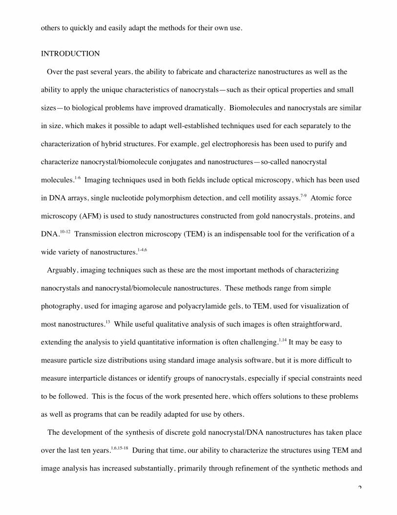
Figure 1. TEM images of heterodimers of 5-nm and 10-nm gold nanocrystals: a) image where
presence of heterodimers is readily apparent by eye, b) image where the presence of heterodimers is
not readily apparent.
Figure 1 shows typical images of heterodimers of 5-nm and 10-nm gold nanocrystals. 50-100
images were analyzed by the programs for each sample. It should be noted, however, that not all
samples are as pure as the one shown in Figure 1. Figures 1a and 1b are both from the same sample,
showing that even in the case of a pure sample, determination and characterization of nanostructures
can benefit from automated image analysis. In addition, data in references 1, 3, and 4 attest to the
power of the programs to discern presence of these lower-yield structures.
For all of the programs, lists of locations and diameters were compiled from the images using
Image Pro; all objects identified by Image Pro within appropriate size ranges were included. These
lists were then used as input for the LabVIEW programs written to calculate pair correlation functions
from the lists of nanocrystal locations or to determine presence of higher order structures.
Descriptions of the general steps included in the programs follow:

6
In the case of heterodimers, two lists were created: one for each size nanocrystal added to the
heterodimer reaction mixture. The distances were calculated between nanocrystals in the two lists.
Then, distances from this list were sorted into 1-nm bins; the number of pairs in each bin was
normalized according to the area of the bin, since bins farther from the nanocrystal have larger area.
The program used to analyze trimers and tetramers worked in a somewhat different manner. Since
the pair correlation functions find only correlations between sets of two nanocrystals, another
approach was needed for more complex nanostructures such as trimers. Seven main steps were
followed; examples are described in the next paragraph and in figure 2. First, the nanocrystals were
again sorted by diameter. Second, a square that has an edge of two times the maximum calculated
diameter of the structure being analyzed was drawn, and all nanocrystals within that box were kept for
the next step in the program. The purpose of this step was to minimize the computations needed for
the subsequent steps. The maximum diameter (dmax) of the structure-of-interest (SOI) was calculated
by adding the radii and DNA lengths of the two particles with the longest DNA length in between
them. In the case of chains of nanocrystals connected by DNA, the dmax would be the end-to-end
distance of the outermost nanocrystals; i.e. the radii of the outer particles, the length of the joining
DNA strands and the diameters of the intermediate gold nanocrystals. Third, distances between the
initial nanocrystal and the others were calculated, and any nanocrystals that were further than one dmax
away were discarded. Fourth, all distances between remaining nanocrystals were checked to
determine that all were within one dmax of one another. Fifth, the number of nanocrystals in the
candidate structure was counted. Sixth, if it was the same as the number of nanocrystals in the SOI, it
was deemed to be an SOI; if the number was different from the number of nanocrystals in the
structure, the program discarded the candidate structure and moved on to the next nanocrystal in the
list. Finally, after a candidate structure was recognized as an SOI, it was verified that none of the
nanocrystals appeared in any other recorded SOI, and if they had not, then the structure was recorded.
It is easy to see why good controls are necessary for this type of analysis. These controls include the

7
analysis of free nanocrystals prepared under the same conditions and analysis of sub-structures.
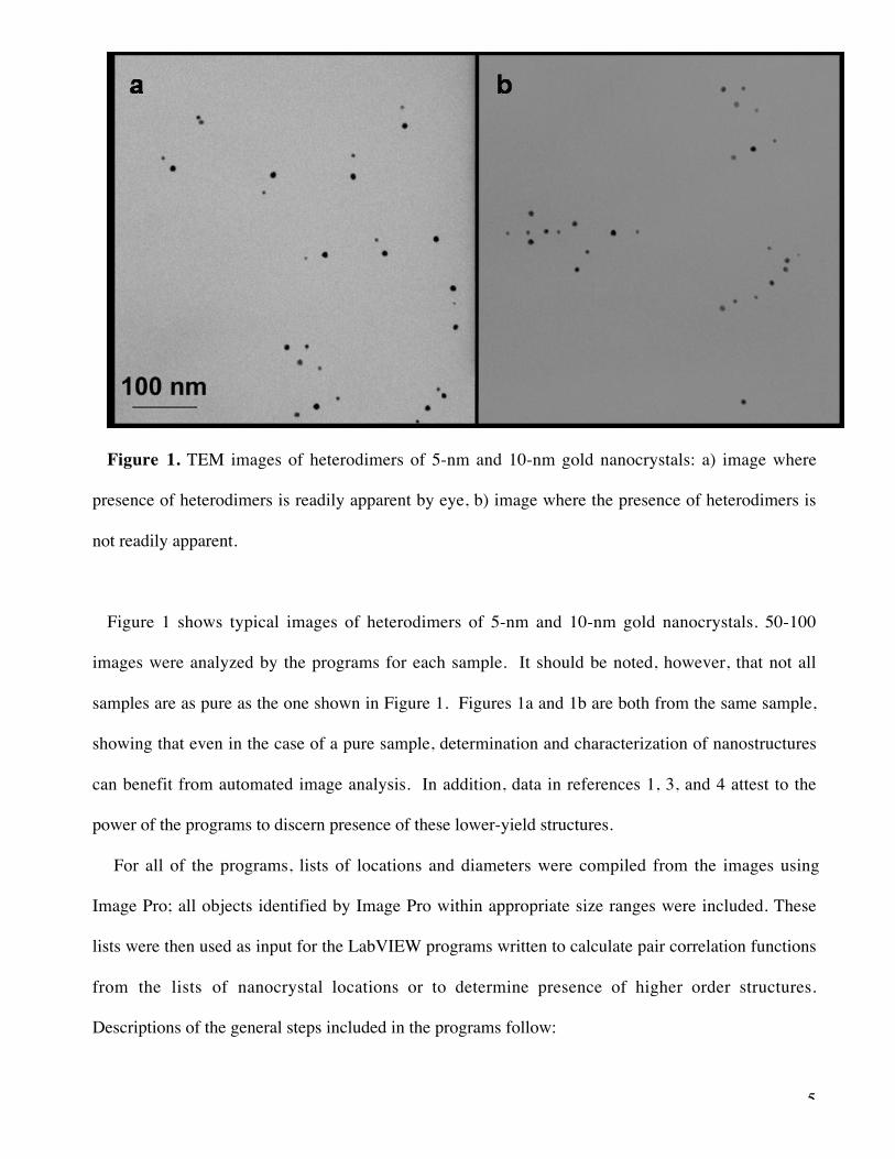
Figure 2. Cartoon showing the operation of several aspects of the structure-finding program.
Figure 2 shows typical situations encountered by a trimer-finding program. In figure 2a an image
with four particles is shown. Particles a, b, and c apparently form a trimer, and particle d is apparently
a free particle. The program would first see particle d and determine the number of particles that are
within two maximum trimer diameters in the x and y directions. In this case, no particles would be
found and the program would move on, since there was no possibility for a trimer to be present. The
program would then move on to particle a. In this case, it would determine that both particles b and c
were within the 2dmax box around particle a. The distances between all the particles would then be
calculated and checked that all were within the dmax of the trimer. Finally, the trimer would be
recorded. In figure 2b, on the other hand, particle d is closer to the trimer. The program would again
start with particle d, but this time it would see that particles a and c are within the 2dmax box around
particle d. The program would measure the distances between all the particles, and determine that
while particles a and d were within one maximum diameter, that c and d were not, causing particle c to
be thrown out. This would leave only two particles, one short of a trimer, and the program would
dmax
2dmax
No distancesNo structure ab<dmax
bc<dmaxac<dmax
3 particlesNo repeatsA trimer!
d
ab
c
da
bc
d closer to abc
da<dmaxac<dmaxdc>dmax
Particle c excluded2 particlesNot a trimer
da<dmaxdb>dmaxdc>dmax
Particle d excluded3 particlesA trimer!
a
b
8
move on to particle a. At particle a, particles b, c, and d would be found to be within the 2dmax box.
The distances between the particles would be calculated, and particle d would be found to be farther
than one maximum diameter from particles b and c, so particle d would be thrown out. This would
leave three particles, and the structure would be counted as a trimer. Finally, in the situation where d
was even closer to c, such that all four particles were within one maximum diameter of one another,
the candidate structure would have too many particles to be counted as a trimer, and it would be
discarded. This situation may be common when the sample is too concentrated on the TEM grid and
may cause undercounting of structures. This was judged to be preferable to the risk of counting
coincidental structures.
Another program was used to determine the presence of higher order structures, which was applied
to the case of hybrid structures of semiconductor and gold nanocrystals linked with DNA. For this
program, it was important to identify a feature distinguishable in ImagePro that would allow division
of the different types of nanocrystals into separate lists. In this case, the semiconductor nanocrystals
were significantly smaller than the gold nanocrystals, so multiple lists were created and compared in a
way similar to the case of heterodimers of nanocrystals explained above.3 Other possibilities may be
contrast (i.e. electron density for TEM images or height for AFM images), shape, aspect ratio, or
others. The structures were located using the method of the trimers and tetramers, described above.
Programs for branched DNA nanocrystal molecules were also developed. These included programs to
analyze the sub-components of the structures. So, the programs for these structures included all the
elements of the homodimer and heterodimer programs, as well as the structure finding programs for
trimers and tetramers; in other words, both distance and particle grouping information was explored.4
Pair Correlation Functions
A number of the results of the utilization of these programs have already been published.1,3,4 Only
brief discussions of those will be offered here, referring the reader to the respective references. Here
we describe the use of the programs by referring to results not previously published, that of

9
heterodimers of 5-nm and 10-nm gold nanocrystals linked with DNA and linear trimers of gold
nanocrystals linked with DNA.
Figure 3. Pair correlation functions of heterodimers. The left-hand column shows 5-10 heterodimers.
The second peak (present only in the left-hand column) corresponds to the interparticle distance in the
corresponding dimers. The arrows for dimer correlations highlight the calculated maximum length of
the dimers. The right-hand column shows heterodimers analyzed using the homodimer program. The
rows correspond to nanocrystals linked with 50-base, 80-base, and 100-base oligonucleotides, from
top to bottom.
Representative images of gold nanocrystal heterodimers consisting of 5-nm and 10-nm nanocrystals
were shown in figure 1. Figure 3 shows the results of the analysis. The left-hand column shows the
results of the pair correlation analysis when the 5-nm and 10-nm particle-size lists were measured
against one another for heterodimers connected by DNA of 50, 80 and 100 bases. The maximum
distance for the heterodimers in each case is expected to be approximately 27, 37 and 44 nm,
respectively. A cut-off at these values is observed in the pair correlation function for all samples. It is
Heterodimers Control
Num
ber
of P
airs
Distance (nm)
50b 50b
80b80b
100b 100b
27nm
37nm
44nm

10
important to note that the strong peak at the nanocrystal diameter was commonly observed and is
attributed to some aggregation on the TEM grid or an artifact from an image processing step.1 The
right-hand column is a control analysis, where the heterodimer images were analyzed for homodimers
of nanocrystals. In the heterodimer sample, there should be no homodimers of 5-nm particles or of 10-
nm particles since the 5-nm particles are attached to DNA complementary to the DNA attached to the
10-nm particles. It can easily be seen that homodimers are not detected in this case. In reference 1, the
corresponding results for homodimers of 5-nm gold nanocrystals and homodimers of 10-nm gold
nanocrystals were presented, showing similar behavior with respect to peak position relative to
maximum calculated particle-particle distances.
There are several other important features of the pair correlation functions to note: there are no pairs
at distances less than the sum of the radii of the nanocrystals, and the baseline is level and non-zero.
Both of these are important checks for verification that the programs are functioning properly. The
baseline is non-zero and level due to random distribution of the dimers relative to one another. If the
bins were not corrected by area, the slope of this baseline would be positive. As the programs
functioned in these experiments, the slope is expected to be negative at longer distances, because of
the finite size of the images; in other words, the ring-shaped bins go off the edges of the images. This
can be corrected by stitching together many images and analyzing them all as one. The effect is
negligible at the distances of interest in these analyses.
A few additional calculations and controls helped to further understand the results of the pair
correlation function data. First, noise is inversely proportional to the square root of the number of
pairs, as expected. So, in order to decrease the noise by half, it is necessary to square the number of
pairs analyzed. This demonstrates the utility of counting by software analysis as compared to hand-
counting. Second, pair correlation functions of purified dimers mixed with varying percentages of
free gold nanocrystals were constructed. These correlation functions showed that an increased
fraction of free gold nanocrystals resulted in a lower fraction of dimers represented in the pair
11
correlation function; however, it became difficult to precisely determine dimer fractions and thus
yields from pair correlation functions. Dimer levels as low as 20% were detectable; no samples at
lower prevalence were tested.
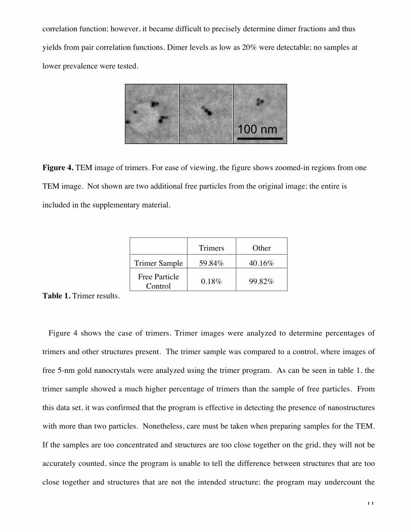
Figure 4. TEM image of trimers. For ease of viewing, the figure shows zoomed-in regions from one
TEM image. Not shown are two additional free particles from the original image; the entire is
included in the supplementary material.
Trimers Other
Trimer Sample 59.84% 40.16%Free Particle
Control 0.18% 99.82%
Table 1. Trimer results.
Figure 4 shows the case of trimers. Trimer images were analyzed to determine percentages of
trimers and other structures present. The trimer sample was compared to a control, where images of
free 5-nm gold nanocrystals were analyzed using the trimer program. As can be seen in table 1, the
trimer sample showed a much higher percentage of trimers than the sample of free particles. From
this data set, it was confirmed that the program is effective in detecting the presence of nanostructures
with more than two particles. Nonetheless, care must be taken when preparing samples for the TEM.
If the samples are too concentrated and structures are too close together on the grid, they will not be
accurately counted, since the program is unable to tell the difference between structures that are too
close together and structures that are not the intended structure; the program may undercount the
100 nm

12
structures in this case. This is part of the intent of this program, since a researcher’s bias may favor
the conclusion that structures are present when this is not objectively the case.
Several sets of more complicated structures have also been analyzed with these programs.
Reference 3 shows both pair correlation function analysis and structure determination analysis for gold
nanocrystals linked to semiconductor nanocrystals with DNA. In this work, the structure finding
program was used to detect the structures, but the pair correlation function program was used to
confirm that the distances correlated with the structures were consistent with the length of DNA
between nanocrystals. This work demonstrated the ability to distinguish between different types of
materials in the programs. While the materials in this case were conveniently different sizes, the
difference could also be determined by image analysis software using shape, aspect ratio, or contrast
limits. Structure analysis has also been conducted for trimers and tetramers of gold nanocrystals
connected with branched DNA. For more information on these structures, see reference 4. Data was
also obtained for samples of symmetric trimers, asymmetric trimers and symmetric tetramers. The
structures as well as their component parts were analyzed using the programs. These data helped to
identify the bands in the gels, as well as strategies for improving yields. The final results can be seen
in the published work.4
Conclusions
The programs developed allowed analysis of more complex nanostructures than was previously
possible, due to reproducible and unbiased methods. It is possible to obtain correlation functions
where the signal to noise ratio is well over three. Counting by hand, a signal-to-noise ratio of at least
three is difficult to obtain at best, and obtaining such a ratio in the case of a bimodal distribution even
more so.
The development of new isolation and characterization tools for nanocrystal/biomolecule structures
must be continued. Several groups have developed or are developing complementary, non-imaging

13
techniques such as small-angle X-ray scattering,19 Coulter counting,20 dielectrophoresis,21 field flow
fractionation,22 and dynamic light scattering.19 AFM is an important imaging technique for
nanostructures as well.11,12 While this paper did not analyze AFM images, the programs presented
should also be useable for AFM images. In particular, it would be interesting to see the programs
applied to network structures, such as those in references 5 and 6, where it should be possible to see
second- and third-nearest neighbor peaks in the pair correlation functions.
ACKNOWLEDGEMENT
C.M.M. thanks the Howard Hughes Medical Institute for the support of a Predoctoral Fellowship.
D.Z. is grateful to FAPESP, Proc. 01/07715-8, and to LNLS for financial support. This work was
supported by the Director, Office of Science, Office of Basic Energy Sciences, Materials Sciences and
Engineering Division, of the U.S. Department of Energy under Contract No. DE-AC02-05CH11231.
SUPPORTING INFORMATION AVAILABLE
LabView code is included of the programs, which are also available at
http://www.cchem.berkeley.edu/pagrp/publications.html. In addition, the full image from figure 4 is
included.
REFERENCES
(1) Zanchet, D.; Micheel, C.M.; Parak, W.J.; Gerion, D.; Williams, S.C.; Alivisatos, A.P. J. Phys.
Chem. B 2002, 106, 11758-11763.
(2) Zanchet, D.; Micheel, C.M.; Parak, W.J.; Gerion, D.; Alivisatos, A.P. Nano Lett. 2001, 1, 32-35.
(3) Fu, A.; Micheel, C.M.; Cha, J.; Chang, H.; Yang, H.; Alivisatos, A.P. J. Am. Chem. Soc. 2004,

14
126, 10832-10833.
(4) Claridge, S.A.; Goh, S.L.; Frechet, J.M.J.; Williams, S.C.; Micheel, C.M.; Alivisatos, A.P.
Chem. Mater. 2005, 17, 1628-1635.
(5) Sharma, J.; Chhabra, R.; Liu, Y.; Ke, Y.; Yan, H. Angew. Chem. Int. Ed. 2006, 45, 730-735.
(6) Zheng, J; Constantinou, P.E.; Micheel, C.; Alivisatos, A.P.; Seeman, N.C. Nano Lett. 2006, 6,
1502-1504.
(7) Gerion, D.; Chen, F.; Kannan, B.; Fu, A.; Parak, W.J.; Chen, D.J.; Majumdar, A.; Alivisatos,
A.P. Anal. Chem. 2003, 75, 4766.
(8) Gerion, D.; Parak, W.J.; Williams, S.C.; Micheel, C.M.; Alivisatos, A.P. J. Am. Chem. Soc.
2002, 124, 7070-7074.
(9) Parak, W.J.; Boudreau, R.; Le Gros, M.; Gerion, D.; Zanchet, D.; Micheel, C.M.; Williams, S.C.;
Alivisatos, A.P.; Larabell, C. Adv. Materials 2002, 14, 882-885.
(10) Rothemund, P.W.K. Nature 2006, 440, 297-302.
(11) Winfree, E.; Liu, F.; Wenzler, L.A.; Seeman, N.C. Nature 1998, 394, 539-544.
(12) Yan, H.; LaBean, T.H.; Feng, L.; Reif, J.H. Proc. Nat. Acad. Sci. 2003, 100, 8103-8108.
(13) Daniel, M.-C.; Astruc, D. Chem. Rev. 2004, 104, 293-346.
(14) Yun, C.S.; Khitrov, G.A.; Vergona, D.E.,; Reich, N.O.; Strouse, G.F. J. Am. Chem. Soc. 2002,
124, 7644-7645.
(15) Alivisatos, A.P.; Johnsson, K.P.; Peng, X.; Wilson, T.E.; Loweth, C.J.; Bruchez, M.P.; Schultz,
P.G. Nature 1996, 382, 609-611.

15
(16) Loweth, C.J.; Caldwell, W.B.; Peng, X.G.; Alivisatos, A.P.; Schultz, P.G. Angew. Chem. Int.
Ed. Engl. 1999, 38, 1808-1812.
(17) Aldaye, F.A.; Sleiman, H.F. Angew. Chem. Int. Ed. 2006, 45, 2204-2209.
(18) Aldaye, F.A.; Sleiman, H.F. J. Am. Chem. Soc. 2007, 129, 4130-4131.
(19) Niemeyer, C.M. Angew. Chem. Int. Ed. 2001, 40, 4128-4158.
(20) Saleh, O.A.; Sohn, L.L. Proc. Nat. Acad. Sci. 2003, 100, 820-824.
(21) Costanzo, P.J.; Liang, E.; Patten, T.E.; Collins, S.D.; Smith, R.L. Lab Chip. 2005, 5, 606-610.
(22) Rameshwar, R.; Samal, S.; Lee, S.; Kim, S.; Cho, J.; Kim, I.S. J. Nanosci. Nanotech. 2006, 6,
2461-2467.

16
SYNOPSIS TOC
Distance (nm)
Num
ber
of P
airs