core i7 lga 2011 guide
TRANSCRIPT

Document Number: 326199-002
Intel® Core™ i7 Processor Family for the LGA2011-0 SocketThermal / Mechanical Specification and Design Guide
Supporting Desktop Intel® Core™ i7-3960X, i7-3970X Extreme Edition Processor, the Intel® Core™ i7-3000K Processor Series, and the Intel® Core™ i7-3000 Processor Series for the LGA2011-0 Socket
November 2012

2 Thermal/Mechanical Specifications and Design Guide
INFORMATION IN THIS DOCUMENT IS PROVIDED IN CONNECTION WITH INTEL® PRODUCTS. NO LICENSE, EXPRESS OR IMPLIED, BY ESTOPPEL OR OTHERWISE, TO ANY INTELLECTUAL PROPERTY RIGHTS IS GRANTED BY THIS DOCUMENT. EXCEPT AS PROVIDED IN INTEL'S TERMS AND CONDITIONS OF SALE FOR SUCH PRODUCTS, INTEL ASSUMES NO LIABILITY WHATSOEVER, AND INTEL DISCLAIMS ANY EXPRESS OR IMPLIED WARRANTY, RELATING TO SALE AND/OR USE OF INTEL PRODUCTS INCLUDING LIABILITY OR WARRANTIES RELATING TO FITNESS FOR A PARTICULAR PURPOSE, MERCHANTABILITY, OR INFRINGEMENT OF ANY PATENT, COPYRIGHT OR OTHER INTELLECTUAL PROPERTY RIGHT. Intel products are not intended for use in medical, life saving, or life sustaining applications. Intel may make changes to specifications and product descriptions at any time, without notice.Designers must not rely on the absence or characteristics of any features or instructions marked “reserved” or “undefined.” Intel reserves these for future definition and shall have no responsibility whatsoever for conflicts or incompatibilities arising from future changes to them.The products in this document may contain design defects or errors known as errata which may cause the product to deviate from published specifications. Current characterized errata are available on request.Contact your local Intel sales office or your distributor to obtain the latest specifications and before placing your product order.“Intel® Turbo Boost Technology requires a PC with a processor with Intel Turbo Boost Technology capability. Intel Turbo Boost Technology performance varies depending on hardware, software and overall system configuration. Check with your PC manufacturer on whether your system delivers Intel Turbo Boost Technology.For more information, see http://www.intel.com/technology/turboboost.”Enhanced Intel® SpeedStep® Technology See the Processor Spec Finder or contact your Intel representative for more information.Intel processor numbers are not a measure of performance. Processor numbers differentiate features within each processor family, not across different processor families. See www.intel.com/products/processor_number for details.Intel, Intel Core, and the Intel logo are trademarks of Intel Corporation in the U.S and other countries.* Other brands and names may be claimed as the property of others.Copyright © 2011, Intel Corporation.
Thermal/Mechanical Specifications and Design Guide 3
Contents
1 Introduction ............................................................................................................ 111.1 References ....................................................................................................... 121.2 Definition of Terms ............................................................................................ 12
2 Package Mechanical Specifications .......................................................................... 152.1 Package Mechanical Specifications ....................................................................... 15
2.1.1 Package Mechanical Drawing.................................................................... 162.1.2 Processor Component Keep-Out Zones...................................................... 162.1.3 Package Loading Specifications ................................................................ 172.1.4 Package Handling Guidelines.................................................................... 172.1.5 Package Insertion Specifications............................................................... 172.1.6 Processor Mass Specification.................................................................... 172.1.7 Processor Materials................................................................................. 182.1.8 Processor Markings................................................................................. 18
3 LGA2011-0 Socket ................................................................................................... 193.1 Contact/Land Mating Location ............................................................................. 223.2 Board Layout .................................................................................................... 223.3 Attachment to Motherboard ................................................................................ 233.4 Socket Components........................................................................................... 24
3.4.1 Socket Body Housing .............................................................................. 243.4.2 Solder Balls ........................................................................................... 243.4.3 Contacts ............................................................................................... 243.4.4 Pick and Place Cover............................................................................... 243.4.5 Socket Standoffs and Package Seating Plane.............................................. 26
3.5 Durability ......................................................................................................... 263.6 Markings .......................................................................................................... 263.7 Component Insertion Forces ............................................................................... 263.8 Socket Size ...................................................................................................... 26
4 Independent Loading Mechanism (ILM)................................................................... 274.1 Square ILM Design Concept ................................................................................ 28
4.1.1 Square ILM Assembly Design Overview ..................................................... 284.2 ILM Features .................................................................................................... 30
4.2.1 ILM Closing sequence ............................................................................. 304.2.2 ILM Opening Sequence............................................................................ 31
4.2.2.1 ILM Keying............................................................................... 334.2.3 ILM Back Plate Design Overview............................................................... 33
4.3 ILM Assembly ................................................................................................... 344.3.1 Manufacturing Assembly Flow .................................................................. 34
4.4 Processor Installation......................................................................................... 354.5 ILM Cover ........................................................................................................ 364.6 Heatsink to ILM interface.................................................................................... 37
5 LGA2011-0 Socket and ILM Electrical, Mechanical, andEnvironmental Specifications................................................................................... 395.1 Component Mass............................................................................................... 395.2 Package/Socket Stackup Height .......................................................................... 395.3 Loading Specifications........................................................................................ 405.4 Electrical Requirements...................................................................................... 405.5 Environmental Requirements .............................................................................. 41
6 Thermal Management Specifications........................................................................ 436.1 Package Thermal Specifications........................................................................... 43
6.1.1 Thermal Specifications ............................................................................ 43
4 Thermal/Mechanical Specifications and Design Guide
6.1.2 TTV TCASE and DTS Based Thermal Specifications........................................446.1.2.1 Thermal Specification.................................................................44
6.1.3 Processor Specification for Operation Where DigitalThermal Sensor Exceeds TCONTROL..........................................................46
6.1.4 Thermal Metrology..................................................................................476.2 Processor Core Thermal Features .........................................................................48
6.2.1 Processor Temperature............................................................................486.2.2 Adaptive Thermal Monitor ........................................................................48
6.2.2.1 Frequency/SVID Control.............................................................496.2.2.2 Clock Modulation.......................................................................50
6.2.3 On-Demand Mode...................................................................................506.2.4 PROCHOT_N Signal .................................................................................506.2.5 THERMTRIP_N Signal ..............................................................................51
6.3 Platform Environment Control Interface (PECI) ......................................................516.3.1 Introduction...........................................................................................516.3.2 PECI Client Capabilities............................................................................52
6.4 Fan Speed Control with Digital Thermal Sensor ......................................................52
7 PECI Interface .........................................................................................................537.1 Platform Environment Control Interface (PECI) ......................................................53
7.1.1 PECI Client Capabilities............................................................................547.1.1.1 Thermal Management ................................................................547.1.1.2 Platform Manageability...............................................................547.1.1.3 Processor Interface Tuning and Diagnostics ..................................54
7.1.2 Client Command Suite.............................................................................557.1.2.1 Ping() ......................................................................................557.1.2.2 GetDIB()..................................................................................567.1.2.3 GetTemp() ...............................................................................587.1.2.4 RdPkgConfig() ..........................................................................597.1.2.5 WrPkgConfig() ..........................................................................617.1.2.6 Package Configuration Capabilities...............................................627.1.2.7 Processor Thermal and Power Optimization Capabilities ..................68
7.1.3 Per Core Temperature Read .....................................................................757.1.4 ACPI P-T Notify Read/Write ......................................................................76
7.1.4.1 Thermally Constrained Time Read................................................767.1.4.2 Current Limit Read ....................................................................767.1.4.3 Accumulated Energy Status Read ................................................767.1.4.4 Power Limit for the VCC Power Plane Write / Read..........................777.1.4.5 Package Power Limits For Multiple Turbo Modes.............................777.1.4.6 Socket Power Limit Performance Status Read................................787.1.4.7 Socket Power-Performance Scalability Read ..................................787.1.4.8 Socket Performance Indication Read ............................................787.1.4.9 RdIAMSR() ...............................................................................797.1.4.10 RdPCIConfig()...........................................................................827.1.4.11 RdPCIConfigLocal()....................................................................847.1.4.12 WrPCIConfigLocal() ...................................................................86
7.1.5 Client Management .................................................................................887.1.5.1 Power-up Sequencing ................................................................887.1.5.2 Device Discovery.......................................................................897.1.5.3 Client Addressing ......................................................................897.1.5.4 C-states...................................................................................907.1.5.5 S-states...................................................................................907.1.5.6 Processor Reset ........................................................................917.1.5.7 Processor Error Handling ............................................................917.1.5.8 Originator Retry and Timeout Policy .............................................927.1.5.9 Enumerating PECI Client Capabilities............................................92
7.1.6 Multi-Domain Commands.........................................................................927.1.7 Client Responses ....................................................................................93
7.1.7.1 Abort FCS ................................................................................93
Thermal/Mechanical Specifications and Design Guide 5
7.1.7.2 Completion Codes ..................................................................... 937.1.8 Originator Responses .............................................................................. 947.1.9 DTS Temperature Data ........................................................................... 95
7.1.9.1 Format .................................................................................... 957.1.9.2 Interpretation........................................................................... 957.1.9.3 Reserved Values ....................................................................... 96
8 Thermal Solutions ................................................................................................... 978.1 Performance Targets.......................................................................................... 97
8.1.1 Reference Heatsink Assembly .................................................................. 978.2 Assembly Process for Reference Heatsinks ............................................................ 988.3 Geometric Envelope for the Intel® Reference ATX Thermal Mechanical Design........... 998.4 Structural Considerations ................................................................................. 1008.5 Attachment to the ILM ..................................................................................... 1008.6 Thermal Interface Material................................................................................ 1008.7 Tall Heat Pipe Heat Sink Performance................................................................. 1018.8 Thermal Design Guidelines ............................................................................... 102
8.8.1 Intel® Turbo Boost 2 Technology ........................................................... 1028.8.2 Thermal Characterization Parameter ....................................................... 1028.8.3 Fan Speed Control ................................................................................ 103
9 Quality and Reliability Requirements ..................................................................... 1059.1 Use Conditions................................................................................................ 1059.2 Intel® Reference Component Validation.............................................................. 106
9.2.1 Board Functional Test Sequence ............................................................. 1069.2.2 Post-Test Pass Criteria Examples ............................................................ 1079.2.3 Recommended BIOS/Processor/Memory Test Procedures ........................... 107
9.3 Material and Recycling Requirements ................................................................. 107
A Mechanical Drawings ............................................................................................. 109
B Socket Mechanical Drawings ................................................................................. 113
C Component Suppliers............................................................................................. 119
D Package Mechanical Drawings ............................................................................... 121
6 Thermal/Mechanical Specifications and Design Guide
Figures1-1 Platform LGA2011-0 Socket Stack with Tall-Heat Pipe Heatsink ...................................112-1 Processor Package Assembly Sketch ........................................................................152-2 Package View .......................................................................................................162-3 Processor Top-Side Markings ..................................................................................183-1 Hexagonal Array in LGA2011-0 ...............................................................................193-2 Contact Wiping Direction ........................................................................................203-3 Schematic of LGA2011-0 Socket with Pick and Place Cover Removed ...........................203-4 LGA2011-0 Socket Contact Numbering (Top View of Socket).......................................213-5 Offset between LGA Land Center and Solder Ball Center .............................................223-6 LGA2011-0 Socket Land Pattern (Top View of Board) .................................................233-7 LGA2011-0 Pick and Place Cover .............................................................................253-8 Pick and Place Cover..............................................................................................254-1 Square ILM Part Terminology..................................................................................284-2 Square ILM Assembly ............................................................................................284-3 ILM as Universal Retention Mechanism.....................................................................294-4 ILM Interlocking Feature ........................................................................................304-5 ILM Lever Closing Sequence ...................................................................................314-6 Opening ILM.........................................................................................................324-7 Opening Sequence for ILM and Loadplate (cont.).......................................................324-8 ILM Keying...........................................................................................................334-9 ILM Back Plate ......................................................................................................334-10 Assembling Socket, Back Plate and ILM onto the Motherboard.....................................344-11 Optional Step: Lock down the Hinge Lever................................................................354-12 Pin 1 Markings on the ILM Frame.............................................................................364-13 Closing ILM and Loadplate......................................................................................364-14 ILM with Cover .....................................................................................................374-15 Heatsink to ILM Interface .......................................................................................385-1 Flow Chart of Knowledge-Based Reliability Evaluation Methodology ..............................416-1 TTV Thermal Profile ...............................................................................................456-2 Case Temperature (TCASE) Measurement Location ....................................................476-3 Frequency and Voltage Ordering .............................................................................497-1 Ping()..................................................................................................................557-2 Ping() Example .....................................................................................................557-3 GetDIB()..............................................................................................................567-4 Device Info Field Definition .....................................................................................567-5 Revision Number Definition.....................................................................................577-6 GetTemp() ...........................................................................................................587-7 GetTemp() Example ..............................................................................................587-8 RdPkgConfig() ......................................................................................................607-9 WrPkgConfig() ......................................................................................................617-10 DRAM Thermal Estimation Configuration Data ...........................................................647-11 DRAM Rank Temperature Write Data .......................................................................657-12 DIMM Temperature Read / Write .............................................................................657-13 Ambient Temperature Reference Data......................................................................667-14 DRAM Channel Temperature ...................................................................................667-15 Accumulated DRAM Energy Data .............................................................................667-16 DRAM Power Info Read Data...................................................................................677-17 DRAM Power Limit Data .........................................................................................677-18 DRAM Power Limit Performance Data .......................................................................687-19 CPUID Data..........................................................................................................717-20 Platform ID Data...................................................................................................717-21 Uncore Device ID ..................................................................................................727-22 Maximum Thread ID ..............................................................................................727-23 Processor Microcode Revision..................................................................................727-24 Package Power SKU Unit Data.................................................................................72
Thermal/Mechanical Specifications and Design Guide 7
7-25 Package Power SKU Data....................................................................................... 737-26 Package Temperature Read Data ............................................................................ 747-27 Temperature Target Read ...................................................................................... 747-28 Thermal Status Word ............................................................................................ 757-29 Thermal Averaging Constant Write / Read................................................................ 757-30 Current Config Limit Read Data .............................................................................. 767-31 Accumulated Energy Read Data .............................................................................. 767-32 Power Limit Data for VCC Power Plane...................................................................... 777-33 PKG_TURBO_POWER_LIMIT Data............................................................................ 777-34 Socket Power Limit Performance Data ..................................................................... 787-35 Socket Power-Performance Scalability Data .............................................................. 787-36 Socket Performance Indication Data ........................................................................ 787-37 Processor ID Construction Example ......................................................................... 807-38 RdIAMSR() .......................................................................................................... 807-39 PCI Configuration Address...................................................................................... 827-40 RdPCIConfig() ...................................................................................................... 837-41 PCI Configuration Address for Local Accesses ........................................................... 847-42 RdPCIConfigLocal() ............................................................................................... 857-43 WrPCIConfigLocal() ............................................................................................... 877-44 Intel® Core™ i7-3960X, i7-3970X Processor Extreme Edition, Intel® Core™ i7-3930K
Processor, and Intel® Core™ i7-3820 Processor PECI Power-up Timeline() ................... 897-45 Temperature Sensor Data Format ........................................................................... 957-46 Temperature Filtering............................................................................................ 958-1 Radial Fin Heatsink Assembly ................................................................................. 978-2 Tall Heat Pipe Heatsink Assembly............................................................................ 988-3 ATX KOZ 3-D Model Primary (Top) Side ................................................................... 998-4 T-HPHS Psi-ca versus RPM ................................................................................... 1018-5 T-HPHS Sound Power (BA) versus RPM .................................................................. 1018-6 Processor Thermal Characterization Parameter Relationships .................................... 103A-1 Board Keepin / Keepout Zones (Sheet 1 of 2) ......................................................... 110A-2 Board Keepin / Keepout Zones (Sheet 2 of 2) ......................................................... 111B-1 Socket Mechanical Drawing (Sheet 1 of 4).............................................................. 114B-2 Socket Mechanical Drawing (Sheet 2 of 4).............................................................. 115B-3 Socket Mechanical Drawing (Sheet 3 of 4).............................................................. 116B-4 Socket Mechanical Drawing (Sheet 4 of 4).............................................................. 117D-1 Processor Package Drawing (Sheet 1 of 2) ............................................................. 122D-2 Processor Package Drawing (Sheet 2of 2) .............................................................. 123
Tables1-1 Reference Documents ........................................................................................... 121-2 Terms and Descriptions ......................................................................................... 122-1 Processor Loading Specifications ............................................................................. 172-2 Package Handling Guidelines .................................................................................. 172-3 Processor Materials ............................................................................................... 183-1 LGA2011-0 Socket Attributes ................................................................................. 194-1 Square ILM Assembly Component Thickness and Material........................................... 295-1 Socket and Retention Component Mass.................................................................... 395-2 2011-land Package and LGA2011-0 Socket Stackup Height ........................................ 395-3 Socket and ILM Mechanical Specifications ................................................................ 405-4 Electrical Requirements for LGA2011-0 Socket.......................................................... 416-1 Processor Thermal Specifications ............................................................................ 446-2 130W TTV Thermal Profile...................................................................................... 456-3 Thermal Solution Performance above TCONTROL for the Intel® Core™ i7-3960X, i7-3970X
Processor Extreme Edition, Intel® Core™ i7-3930K Processor, and Intel® Core™ i7-3820 Processor ............................................................................................................ 46
8 Thermal/Mechanical Specifications and Design Guide
7-1 Summary of Processor-specific PECI Commands........................................................537-2 Minor Revision Number Meaning..............................................................................577-3 GetTemp() Response Definition...............................................................................597-4 RdPkgConfig() Response Definition ..........................................................................607-5 WrPkgConfig() Response Definition..........................................................................627-6 RdPkgConfig() & WrPkgConfig() DRAM Thermal Services Summary..............................637-7 Channel & DIMM Index decoding .............................................................................647-8 RdPkgConfig() & WrPkgConfig() Processor Thermal and Power Optimization
Services Summary ................................................................................................687-9 Platform ID Encoding.............................................................................................717-10 Power Control Register Unit Calculations ..................................................................737-11 RdIAMSR() Response Definition...............................................................................817-12 RdIAMSR() Services Summary ................................................................................817-13 RdPCIConfig() Response Definition ..........................................................................837-14 RdPCIConfigLocal() Response Definition ...................................................................857-15 WrPCIConfigLocal() Response Definition ...................................................................877-16 WrPCIConfigLocal() Memory Controller Device/Function Support..................................887-17 PECI Client Response During Power-Up ....................................................................887-18 SOCKET ID Strapping ............................................................................................897-19 Power Impact of PECI Commands versus C-states .....................................................907-20 Domain ID Definition .............................................................................................927-21 Multi-Domain Command Code Reference ..................................................................937-22 Completion Code Pass/Fail Mask..............................................................................937-23 Device Specific Completion Code (CC) Definition........................................................947-24 Originator Response Guidelines ...............................................................................947-25 Error Codes and Descriptions ..................................................................................968-1 Processor Reference Thermal Boundary Conditions ....................................................978-2 Reference Heat Sink Clearance above the Motherboard ..............................................998-3 Intel® Reference Thermal Solution TIM..................................................................1008-4 Fan Speed Control, TCONTROL and DTS Relationship ...............................................1039-1 Use Conditions Environment (System Level) ...........................................................1059-2 Use Conditions Environment (System Level) ...........................................................106A-1 Mechanical Drawing List .......................................................................................109B-1 Socket Drawing List.............................................................................................113C-1 Suppliers for the Intel® Reference Thermal Solutions ...............................................119C-2 Suppliers for the LGA2011-0 Socket and ILM ..........................................................120C-3 Suppliers for the LGA-2011-0 Socket and ILM (Continued)........................................120D-1 Mechanical Drawing List .......................................................................................121
Thermal/Mechanical Specifications and Design Guide 9
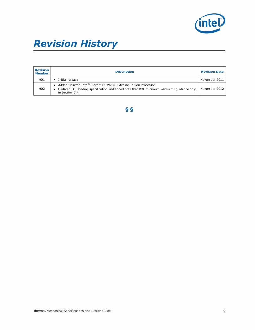
Revision History
§ §
Revision Number Description Revision Date
001 • Initial release November 2011
002• Added Desktop Intel® Core™ i7-3970X Extreme Edition Processor• Updated EOL loading specification and added note that BOL minimum load is for guidance only,
in Section 5.4,November 2012

10 Thermal/Mechanical Specifications and Design Guide
Thermal/Mechanical Specifications and Design Guide 11
Introduction
1 Introduction
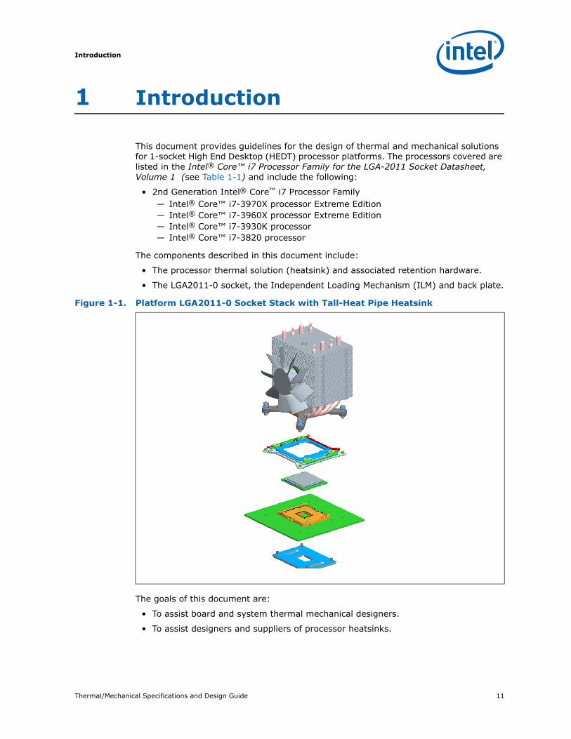
This document provides guidelines for the design of thermal and mechanical solutions for 1-socket High End Desktop (HEDT) processor platforms. The processors covered are listed in the Intel® Core™ i7 Processor Family for the LGA-2011 Socket Datasheet, Volume 1 (see Table 1-1) and include the following:
• 2nd Generation Intel® Core™ i7 Processor Family — Intel® Core™ i7-3970X processor Extreme Edition— Intel® Core™ i7-3960X processor Extreme Edition— Intel® Core™ i7-3930K processor— Intel® Core™ i7-3820 processor
The components described in this document include:
• The processor thermal solution (heatsink) and associated retention hardware.
• The LGA2011-0 socket, the Independent Loading Mechanism (ILM) and back plate.
The goals of this document are:
• To assist board and system thermal mechanical designers.
• To assist designers and suppliers of processor heatsinks.
Figure 1-1. Platform LGA2011-0 Socket Stack with Tall-Heat Pipe Heatsink
Introduction
12 Thermal/Mechanical Specifications and Design Guide
1.1 ReferencesMaterial and concepts available in the following documents may be beneficial when reading this document.
1.2 Definition of Terms
Table 1-1. Reference Documents
Document Location
Intel® Core™ i7 Processor Family for the LGA-2011 Socket Datasheet, Volume 1 326196
Intel® Core™ i7 Processor Family for the LGA-2011 Socket Datasheet, Volume 2 326197
Intel® Core™ i7 Processor Family for the LGA-2011 Socket Specification Update 326198
Entry-level Electronics Bay Specification Available at http://ssiforum.oaktree.com/
European Blue Angel Recycling Standards http://www.blauer-engel.de
Table 1-2. Terms and Descriptions (Sheet 1 of 2)
Term Description
BypassBypass is the area between a passive heatsink and any object that can act to form a duct. For this example, it can be expressed as a dimension away from the outside dimension of the fins to the nearest surface.
DTS Digital Thermal Sensor reports a relative die temperature as an offset from TCC activation temperature.
MSRThe processor provides a variety of model specific registers that are used to control and report on processor performance. Virtually all MSRs handle system related functions and are not accessible to an application program.
FSC Fan Speed Control
IHSIntegrated Heat Spreader: a component of the processor package used to enhance the thermal performance of the package. Component thermal solutions interface with the processor at the IHS surface.
Square ILM
Independent Loading Mechanism provides the force needed to seat the 2011-LGA package onto the socket contacts and has 80 × 80 mm heatsink mounting hole pattern. The Customer Reference Board will use this layout. The enabled Thermal solutions are only compatible with this ILM.
LGA2011-0 socket The processor mates with the system board through this surface mount, 2011-contact socket for the platform.
PECIThe Platform Environment Control Interface (PECI) is a one-wire interface that provides a communication channel between Intel processor and chipset components to external monitoring devices.
ΨCA
Case-to-ambient thermal characterization parameter (psi). A measure of thermal solution performance using total package power. Defined as (TCASE – TLA) / Total Package Power. Heat source should always be specified for Ψ measurements.
ΨCS
Case-to-sink thermal characterization parameter. A measure of thermal interface material performance using total package power. Defined as (TCASE – TS) / Total Package Power.
ΨSASink-to-ambient thermal characterization parameter. A measure of heatsink thermal performance using total package power. Defined as (TS – TLA) / Total Package Power.
TCASEThe case temperature of the processor measured at the geometric center of the topside of the IHS.
TCASE_MAX The maximum case temperature as specified in a component specification.
TCCThermal Control Circuit: Thermal monitor uses the TCC to reduce the die temperature by using clock modulation and/or operating frequency and input voltage adjustment when the die temperature is very near its operating limits.

Thermal/Mechanical Specifications and Design Guide 13
Introduction
§
TCONTROLTCONTROL is a static value below TCC activation used as a trigger point for fan speed control. When DTS > TCONTROL, the processor must comply to the thermal profile.
TDP Thermal Design Power: Thermal solution should be designed to dissipate this target power level. TDP is not the maximum power that the processor can dissipate.
Thermal Monitor A power reduction feature designed to decrease temperature after the processor has reached its maximum operating temperature.
Thermal Profile Line that defines case temperature specification of a processor at a given power level.
TIMThermal Interface Material: The thermally conductive compound between the heatsink and the processor case. This material fills the air gaps and voids, and enhances the transfer of the heat from the processor case to the heatsink.
TLA
The measured ambient temperature locally surrounding the processor. The ambient temperature should be measured just upstream of a passive heatsink or at the fan inlet for an active heatsink.
TSAThe system ambient air temperature external to a system chassis. This temperature is usually measured at the chassis air inlets.
Table 1-2. Terms and Descriptions (Sheet 2 of 2)
Term Description

Introduction
14 Thermal/Mechanical Specifications and Design Guide

Thermal/Mechanical Specifications and Design Guide 15
Package Mechanical Specifications
2 Package Mechanical Specifications
2.1 Package Mechanical SpecificationsThe Intel® Core™ i7-3960X, i7-3970X processor Extreme Edition, Intel® Core™ i7-3930K processor, and Intel® Core™ i7-3820 processor are packaged in a 2011-land Flip-Chip Land Grid Array package that interfaces with the baseboard using the LGA2011-0 socket. The package consists of a processor mounted on a substrate land-carrier. An integrated heat spreader (IHS) is attached to the package substrate and core and serves as the mating surface for processor component thermal solutions, such as a heatsink. Figure 2-1 shows a sketch of the processor package components and how they are assembled together. Refer to Chapter 3, 4 and 5 for complete details on the LGA2011-0 socket and ILM.
The package components shown in Figure 2-1 include the following:
1. Integrated Heat Spreader (IHS)2. Thermal Interface Material (TIM)
3. Processor (die)
4. Package substrate
5. Capacitors
Note:1. Socket and baseboard are included for reference and are not part of processor package.
Figure 2-1. Processor Package Assembly Sketch
IHS
Substrate
LGA 2011-0 Socket
System Board
Capacitors
DIE TIM
Package Mechanical Specifications
16 Thermal/Mechanical Specifications and Design Guide
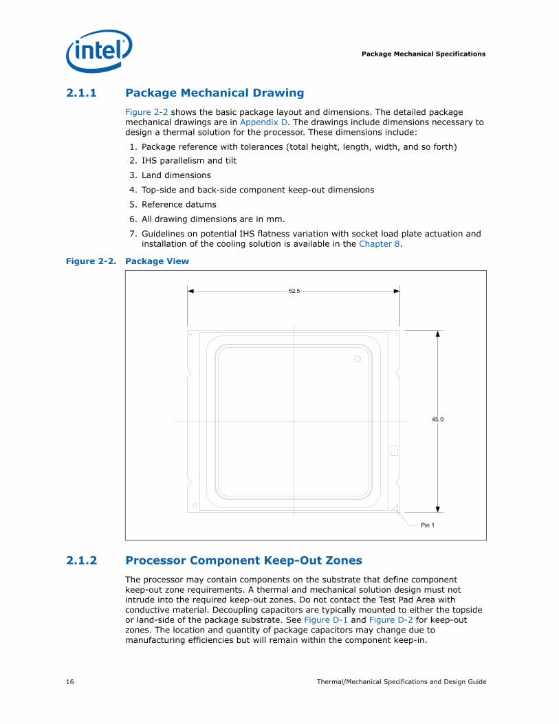
2.1.1 Package Mechanical DrawingFigure 2-2 shows the basic package layout and dimensions. The detailed package mechanical drawings are in Appendix D. The drawings include dimensions necessary to design a thermal solution for the processor. These dimensions include:
1. Package reference with tolerances (total height, length, width, and so forth)2. IHS parallelism and tilt
3. Land dimensions
4. Top-side and back-side component keep-out dimensions
5. Reference datums
6. All drawing dimensions are in mm.
7. Guidelines on potential IHS flatness variation with socket load plate actuation and installation of the cooling solution is available in the Chapter 8.
2.1.2 Processor Component Keep-Out ZonesThe processor may contain components on the substrate that define component keep-out zone requirements. A thermal and mechanical solution design must not intrude into the required keep-out zones. Do not contact the Test Pad Area with conductive material. Decoupling capacitors are typically mounted to either the topside or land-side of the package substrate. See Figure D-1 and Figure D-2 for keep-out zones. The location and quantity of package capacitors may change due to manufacturing efficiencies but will remain within the component keep-in.
Figure 2-2. Package View
52.5
45.0
Pin 1

Thermal/Mechanical Specifications and Design Guide 17
Package Mechanical Specifications
2.1.3 Package Loading Specifications Table 2-1 provides load specifications for the processor package. These maximum limits should not be exceeded during heatsink assembly, shipping conditions, or standard use condition. Exceeding these limits during test may result in component failure. The processor substrate should not be used as a mechanical reference or load-bearing surface for thermal solutions.
.
Notes:1. These specifications apply to uniform compressive loading in a direction normal to the processor IHS.2. This is the maximum static force that can be applied by the heatsink and Independent Loading Mechanism
(ILM). 3. These specifications are based on limited testing for design characterization. Loading limits are for the
package constrained by the limits of the processor socket. 4. Dynamic loading is defined the maximum heatsink mass from Table 5-3 with an 11 ms duration average
load superimposed on the static load requirement.5. See Section 5.3 for minimum socket load to engage processor within socket.
2.1.4 Package Handling GuidelinesTable 2-2 includes a list of guidelines on package handling in terms of recommended maximum loading on the processor IHS relative to a fixed substrate. These package handling loads may be experienced during heatsink removal.
2.1.5 Package Insertion SpecificationsThe processor can be inserted into and removed from an LGA2011-0 socket 15 times. The socket should meet the LGA2011-0 requirements detailed in Chapter 3 and Chapter 5.
2.1.6 Processor Mass SpecificationThe typical mass of the processor is currently 45 grams. This mass [weight] includes all the components that are included in the package.
Table 2-1. Processor Loading Specifications
Parameter Maximum Notes
Static Compressive Load 1067 N [240 lbf] 1, 2, 3, 5
Dynamic Load 589 N [132 lbf] 1, 3, 4, 5
Table 2-2. Package Handling Guidelines
Parameter Maximum Recommended Notes
Shear 80 lbs (36.287 kg)
Tensile 35 lbs (15.875 kg)
Torque 35 in.lbs (15.875 kg-cm)
Package Mechanical Specifications
18 Thermal/Mechanical Specifications and Design Guide
2.1.7 Processor MaterialsTable 2-3 lists some of the package components and associated materials.
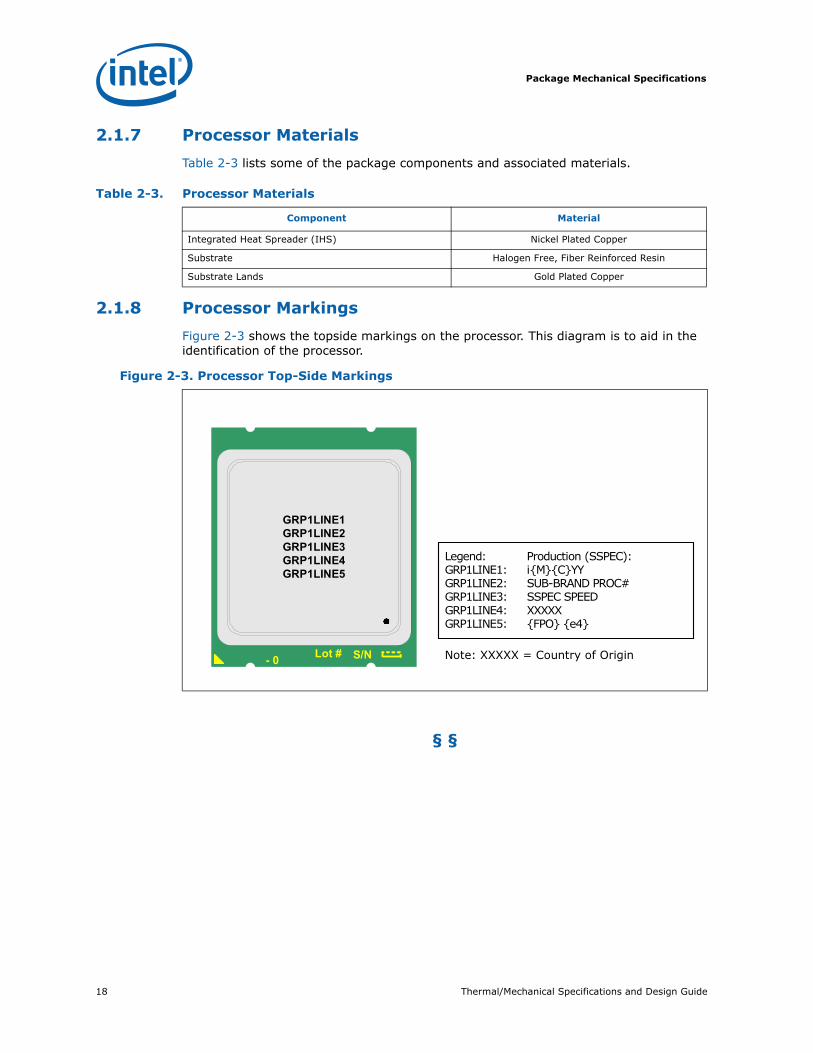
2.1.8 Processor MarkingsFigure 2-3 shows the topside markings on the processor. This diagram is to aid in the identification of the processor.
§ §
Table 2-3. Processor Materials
Component Material
Integrated Heat Spreader (IHS) Nickel Plated Copper
Substrate Halogen Free, Fiber Reinforced Resin
Substrate Lands Gold Plated Copper
Figure 2-3. Processor Top-Side Markings
S/N- 0
GRP1LINE1GRP1LINE2GRP1LINE3GRP1LINE4GRP1LINE5
Legend: Sample (QDF):GRP1LINE1: i{M}{C}YYGRP1LINE2: INTEL CONFIDENTIALGRP1LINE3: QDF ES SPEEDGRP1LINE4: XXXXXGRP1LINE5: {FPO} {e4}
Legend: Production (SSPEC):GRP1LINE1: i{M}{C}YY GRP1LINE2: SUB-BRAND PROC#GRP1LINE3: SSPEC SPEEDGRP1LINE4: XXXXXGRP1LINE5: {FPO} {e4}
Lot # Note: XXXXX = Country of Origin
Thermal/Mechanical Specifications and Design Guide 19
LGA2011-0 Socket
3 LGA2011-0 Socket
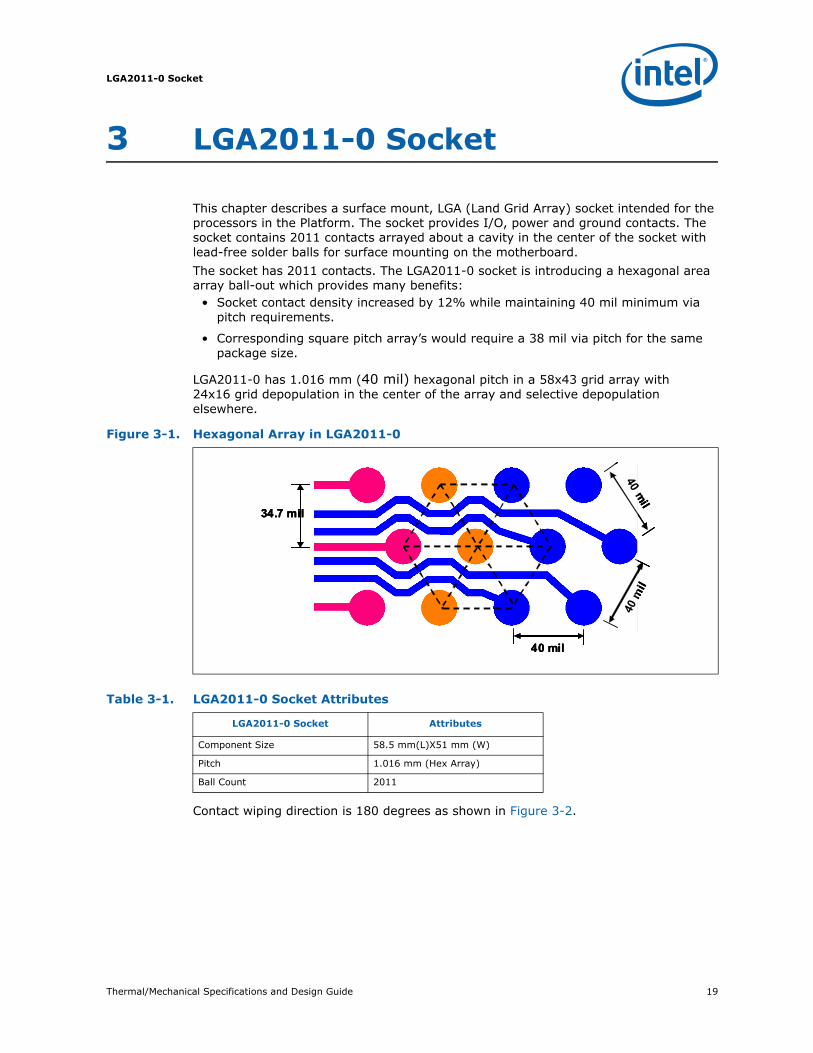
This chapter describes a surface mount, LGA (Land Grid Array) socket intended for the processors in the Platform. The socket provides I/O, power and ground contacts. The socket contains 2011 contacts arrayed about a cavity in the center of the socket with lead-free solder balls for surface mounting on the motherboard.The socket has 2011 contacts. The LGA2011-0 socket is introducing a hexagonal area array ball-out which provides many benefits:
• Socket contact density increased by 12% while maintaining 40 mil minimum via pitch requirements.
• Corresponding square pitch array’s would require a 38 mil via pitch for the same package size.
LGA2011-0 has 1.016 mm (40 mil) hexagonal pitch in a 58x43 grid array with 24x16 grid depopulation in the center of the array and selective depopulation elsewhere.
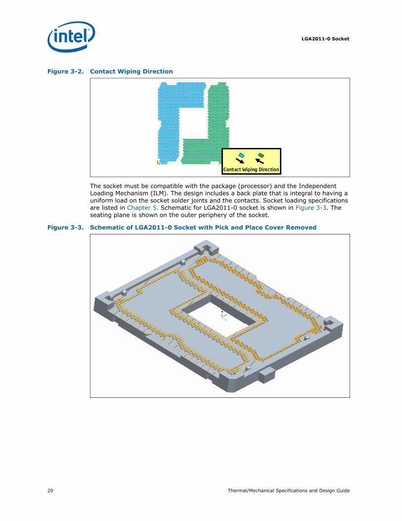
Contact wiping direction is 180 degrees as shown in Figure 3-2.
Figure 3-1. Hexagonal Array in LGA2011-0
Table 3-1. LGA2011-0 Socket Attributes
LGA2011-0 Socket Attributes
Component Size 58.5 mm(L)X51 mm (W)
Pitch 1.016 mm (Hex Array)
Ball Count 2011
40 m
il
40 mil
40 mil
34.7 mil
40 m
il
40 mil
40 mil
34.7 mil
40 m
il
40 mil
40 mil
34.7 mil
LGA2011-0 Socket
20 Thermal/Mechanical Specifications and Design Guide
The socket must be compatible with the package (processor) and the Independent Loading Mechanism (ILM). The design includes a back plate that is integral to having a uniform load on the socket solder joints and the contacts. Socket loading specifications are listed in Chapter 5. Schematic for LGA2011-0 socket is shown in Figure 3-3. The seating plane is shown on the outer periphery of the socket.
Figure 3-2. Contact Wiping Direction
Contact Wiping DirectionContact Wiping DirectionContact Wiping Direction
Figure 3-3. Schematic of LGA2011-0 Socket with Pick and Place Cover Removed
Thermal/Mechanical Specifications and Design Guide 21
LGA2011-0 Socket
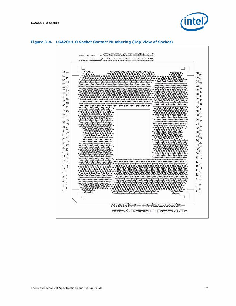
Figure 3-4. LGA2011-0 Socket Contact Numbering (Top View of Socket)
LGA2011-0 Socket
22 Thermal/Mechanical Specifications and Design Guide
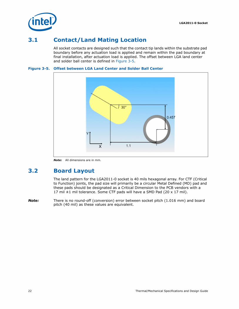
3.1 Contact/Land Mating LocationAll socket contacts are designed such that the contact tip lands within the substrate pad boundary before any actuation load is applied and remain within the pad boundary at final installation, after actuation load is applied. The offset between LGA land center and solder ball center is defined in Figure 3-5.
Note: All dimensions are in mm.
3.2 Board LayoutThe land pattern for the LGA2011-0 socket is 40 mils hexagonal array. For CTF (Critical to Function) joints, the pad size will primarily be a circular Metal Defined (MD) pad and these pads should be designated as a Critical Dimension to the PCB vendors with a 17 mil ±1 mil tolerance. Some CTF pads will have a SMD Pad (20 x 17 mil).
Note: There is no round-off (conversion) error between socket pitch (1.016 mm) and board pitch (40 mil) as these values are equivalent.
Figure 3-5. Offset between LGA Land Center and Solder Ball Center
Thermal/Mechanical Specifications and Design Guide 23
LGA2011-0 Socket
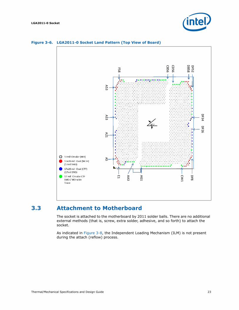
3.3 Attachment to MotherboardThe socket is attached to the motherboard by 2011 solder balls. There are no additional external methods (that is, screw, extra solder, adhesive, and so forth) to attach the socket.
As indicated in Figure 3-8, the Independent Loading Mechanism (ILM) is not present during the attach (reflow) process.
Figure 3-6. LGA2011-0 Socket Land Pattern (Top View of Board)
LGA2011-0 Socket
24 Thermal/Mechanical Specifications and Design Guide
3.4 Socket ComponentsThe socket has two main components, the socket body and Pick and Place (PnP) cover, and is delivered as a single integral assembly. Refer to Appendix B for detailed drawings.
3.4.1 Socket Body HousingThe housing material is thermoplastic or equivalent with UL 94 V-0 flame rating capable of withstanding 260 °C for 40 seconds (typical reflow/rework). The socket coefficient of thermal expansion (in the XY plane), and creep properties, must be such that the integrity of the socket is maintained for the conditions listed in Chapter 9.
The color of the housing will be dark as compared to the solder balls to provide the contrast needed for pick and place vision systems.
3.4.2 Solder BallsA total of 2011 solder balls corresponding to the contacts are on the bottom of the socket for surface mounting with the motherboard.
The socket has the following solder ball material:
• Lead free SAC305(SnAgCu) solder alloy with a silver (Ag) content 3%, copper (Cu) 0.5%,tin (Sn) 96.5% and a melting temperature of approximately 217 °C. The immersion silver (ImAg) motherboard surface finish and solder paste alloy must be compatible with the SAC alloy solder paste.
The co-planarity (profile) and true position requirements are defined in Appendix B.
3.4.3 ContactsThe base material for the contacts is high strength copper alloy.
For the area on socket contacts where processor lands will mate, there is a 0.381 μm [15 μinches] minimum gold plating over 1.27 μm [50 μinches] minimum nickel underplate.
No contamination by solder in the contact area is allowed during solder reflow.
3.4.4 Pick and Place CoverThe cover provides a planar surface for vacuum pick up used to place components in the Surface Mount Technology (SMT) manufacturing line. The cover remains on the socket during reflow to help prevent contamination during reflow. The cover can withstand 260 °C for 40 seconds (typical reflow/rework profile) and the conditions listed in Chapter 9 without degrading.

Thermal/Mechanical Specifications and Design Guide 25
LGA2011-0 Socket
As indicated in Figure 3-8, the pick and place (PnP) cover remains on the socket during ILM installation. Once the ILM with its cover is installed, Intel is recommending the PnP cover be removed to help prevent damage to the socket contacts. To reduce the risk of bent contacts the PnP Cover and ILM Cover were designed to not be compatible. See Section 4.3 for additional information on ILM assembly to the board.
Cover retention must be sufficient to support the socket weight during lifting, translation, and placement (board manufacturing), and during board and system shipping and handling. Covers can be removed without tools.
The pick and place covers are designed to be interchangeable between socket suppliers.
Note: Figure is representative and may not show the most current revision of parts.
Figure 3-7. LGA2011-0 Pick and Place Cover
Figure 3-8. Pick and Place Cover
Pick and Place Cover
ILM
LGA2011-0 Socket
26 Thermal/Mechanical Specifications and Design Guide
3.4.5 Socket Standoffs and Package Seating PlaneStandoffs on the bottom of the socket base establish the minimum socket height after solder reflow and are specified in Appendix B.
Similarly, a seating plane on the topside of the socket establishes the minimum package height. See Section 5.2 for the calculated IHS height above the motherboard.
3.5 DurabilityThe socket must withstand 30 cycles of processor insertion and removal. The maximum part average and single pin resistances from Table 5-4 must be met when mated in the 1st and 30th cycles.
The socket Pick and Place cover must withstand 15 cycles of insertion and removal.
3.6 MarkingsThere are three markings on the socket:
• LGA2011-0: Font type is Helvetica Bold - minimum 6 point (2.125 mm).
• Manufacturer's insignia (font size at supplier's discretion).
• Lot identification code (allows traceability of manufacturing date and location).
All markings must withstand 260 °C for 40 seconds (typical reflow/rework profile) without degrading, and must be visible after the socket is mounted on the motherboard.
LGA2011-0 and the manufacturer's insignia are molded or laser marked on the side wall.
3.7 Component Insertion ForcesAny actuation must meet or exceed SEMI S8-95 Safety Guidelines for Ergonomics/Human Factors Engineering of Semiconductor Manufacturing Equipment, example Table R2-7 (Maximum Grip Forces). The socket must be designed so that it requires no force to insert the package into the socket.
3.8 Socket SizeSocket information needed for motherboard design is given in Appendix B.
This information should be used in conjunction with the reference motherboard keep-out drawings provided in Appendix A to ensure compatibility with the reference thermal mechanical components.
§
Thermal/Mechanical Specifications and Design Guide 27
Independent Loading Mechanism (ILM)
4 Independent Loading Mechanism (ILM)
The Independent Loading Mechanism (ILM) provides the force needed to seat the 2011-land LGA package onto the socket contacts. The ILM is physically separate from the socket body. The assembly of the ILM is expected to occur after attaching the socket to the board. The exact assembly location is dependent on manufacturing preference and test flow.
The mechanical design of the ILM is a key contributor to the overall functionality of the LGA2011-0 socket. Intel performs detailed studies on integration of processor package, socket and ILM as a system. These studies directly impact the design of the ILM. The Intel reference ILM will be “built to print” from Intel controlled drawings. Intel recommends using the Intel Reference ILM. Custom non-Intel ILM designs do not benefit from Intel's detailed studies and may not incorporate critical design parameters.
Note: The ILM has two critical functions: deliver the force to seat the processor onto the socket contacts and distribute the resulting load evenly through the socket solder joints. Another purpose of ILM is to ensure electrical integrity/performance of the socket and package.
Note: This design will be “built to print” from Intel controlled drawings.
Independent Loading Mechanism (ILM)
28 Thermal/Mechanical Specifications and Design Guide
4.1 Square ILM Design ConceptThe square ILM consists of two assemblies that will be procured as a set from the enabled vendors. These two components are the ILM assembly and back plate.
4.1.1 Square ILM Assembly Design Overview
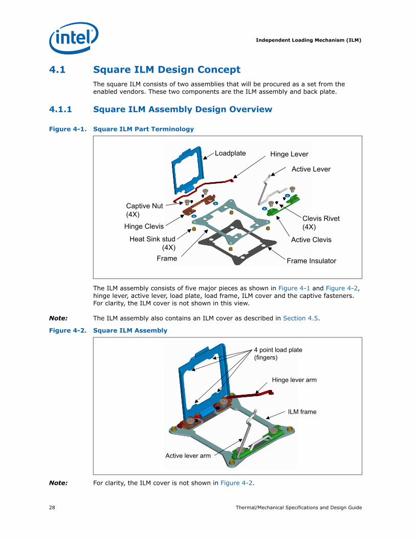
The ILM assembly consists of five major pieces as shown in Figure 4-1 and Figure 4-2, hinge lever, active lever, load plate, load frame, ILM cover and the captive fasteners. For clarity, the ILM cover is not shown in this view.
Note: The ILM assembly also contains an ILM cover as described in Section 4.5.
Note: For clarity, the ILM cover is not shown in Figure 4-2.
Figure 4-1. Square ILM Part Terminology
Loadplate Hinge LeverLoadplate
Active Lever
Hinge Lever
Captive Nut(4X) C
Active Clevis
Hinge Clevis
(4X)
Heat Sink stud(4X)
Clevis Rivet(4X)
Frame Insulator
(4X)Frame
Figure 4-2. Square ILM Assembly
4 point load plate(fingers)
Hinge lever arm
ILM frame
Active lever arm

Thermal/Mechanical Specifications and Design Guide 29
Independent Loading Mechanism (ILM)
The hinge lever and active lever are designed to place equal force on both ends of the ILM load plate. The frame provides the hinge locations for the levers. The hinge lever connects the load plate to the frame. When closed, the load plate applies four point loads onto the IHS at the “finger” features shown in Figure 4-2. Four point loading contributes to minimizing package and socket warpage as compared to two point loading. The reaction force from closing the load plate is transmitted to the frame and through the captive fasteners to the back plate. Some of the load is passed through the socket body to the board inducing a slight compression on the solder joints.
Figure 4-3 shows the attachment points of the thermal solution to the ILM frame and the ILM to the back plate. This attachment method requires four holes in the motherboard for the ILM and no additional holes for the thermal solution. Orientation of the ILM is controlled with a key on the socket body. Orientation of the thermal solution is an option with a key to the ILM.
Note: Some customer reference boards (CRB) have four additional outer holes in the board. These holes are legacy and are not required for the current ILM reference design.
Table 4-1. Square ILM Assembly Component Thickness and Material
Component Thickness (mm) Material
ILM Frame 1.5 301 Stainless Steel
ILM Loadplate 1.5 301 Stainless Steel
ILM Backplate 2.2 S50C Low Carbon Steel
Figure 4-3. ILM as Universal Retention Mechanism

Independent Loading Mechanism (ILM)
30 Thermal/Mechanical Specifications and Design Guide
4.2 ILM Features• Allows for topside thermal solution attach to a rigid structure. This eliminates the
motherboard thickness dependency from the mechanical stackup.
• Captive nuts clamp the ILM frame to the board and reduced board bending leading to higher solder joint reliability.
• ILM levers provide an interlocking mechanism to ensure proper opening or closing sequence for the operator.
4.2.1 ILM Closing sequenceWhen closing the ILM, the interlocking features are intended to prevent the hinge lever from being latched first. If an attempt is made to close the hinge lever first, the hinge lever end stop will prevent the user from latching the active lever, indicating something is done wrong. Text on the ILM cover indicates the proper order of operation. Refer to Figure 4-4.
If hinge lever is pressed down first, it raises the load plate up at an angle higher than the active lever can make contact with, forcing a user to push it down. Also the hinge lever end stop will block the active lever from being able to be latched.
Figure 4-4. ILM Interlocking Feature
Hinge Lever
I t l ki f tInterlocking featureon hinge lever. Active Lever.

Thermal/Mechanical Specifications and Design Guide 31
Independent Loading Mechanism (ILM)
ILM lever closing sequence is shown in Figure 4-5.
1. Latch Active Lever first.2. Close Hinge Lever second.
Note: The ILM closing sequence is marked on the ILM load plate.
4.2.2 ILM Opening SequenceFor the opening sequence, the goal is to always open the hinge lever first to prevent the loadplate from springing open. The only option is to release the hinge lever first. The hinge lever in a closed position will block the active lever from being unlatched. By opening hinge lever first, it creates clearance to open the active lever.
Figure 4-5. ILM Lever Closing Sequence
Step 1Close Active Lever
Step 2Step 2Close Hinge Lever

Independent Loading Mechanism (ILM)
32 Thermal/Mechanical Specifications and Design Guide
The ILM opening sequence is shown in Figure 4-6.
1. Open hinge lever2. Open active lever
Note: The opening sequence is also marked on the ILM load plate
3. Open the load plate by pushing down on the hinge lever Figure 4-7, this will cause the load plate tab to rise above the socket. Grasp the tab, only after it has risen away from the socket, open load plate to full open position.
Note: ILM cover not shown for clarity.
Figure 4-6. Opening ILM
Opening the hinge lever provides the clearance to open the active lever
Step 1Open Hinge Lever
Step 2Open Active Lever
Figure 4-7. Opening Sequence for ILM and Loadplate (cont.)
Thermal/Mechanical Specifications and Design Guide 33
Independent Loading Mechanism (ILM)
4.2.2.1 ILM Keying
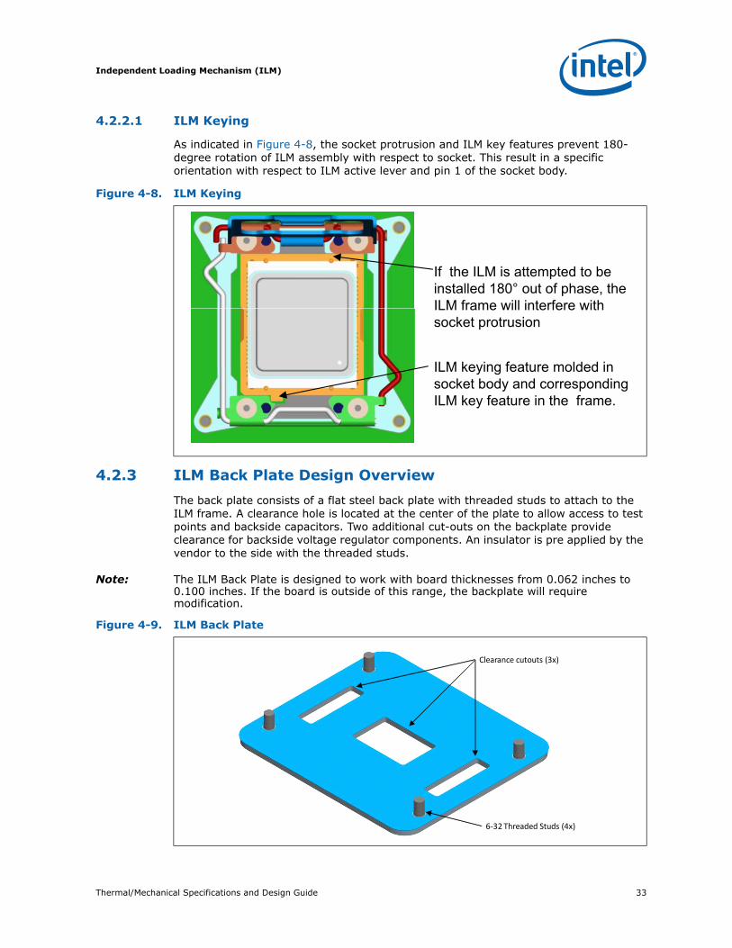
As indicated in Figure 4-8, the socket protrusion and ILM key features prevent 180-degree rotation of ILM assembly with respect to socket. This result in a specific orientation with respect to ILM active lever and pin 1 of the socket body.
4.2.3 ILM Back Plate Design OverviewThe back plate consists of a flat steel back plate with threaded studs to attach to the ILM frame. A clearance hole is located at the center of the plate to allow access to test points and backside capacitors. Two additional cut-outs on the backplate provide clearance for backside voltage regulator components. An insulator is pre applied by the vendor to the side with the threaded studs.
Note: The ILM Back Plate is designed to work with board thicknesses from 0.062 inches to 0.100 inches. If the board is outside of this range, the backplate will require modification.
Figure 4-8. ILM Keying
If the ILM is attempted to be installed 180° out of phase, the ILM frame will interfere with
ILM keying feature molded in
ILM frame will interfere withsocket protrusion
ILM keying feature molded insocket body and corresponding ILM key feature in the frame.
Figure 4-9. ILM Back Plate
Clearance cutouts (3x)
6-32 Threaded Studs (4x)
Independent Loading Mechanism (ILM)
34 Thermal/Mechanical Specifications and Design Guide
4.3 ILM AssemblyNote: The ILM assembly instructions shown here are for illustration.
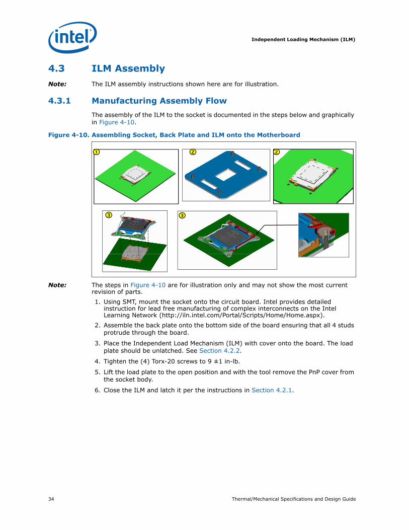
4.3.1 Manufacturing Assembly FlowThe assembly of the ILM to the socket is documented in the steps below and graphically in Figure 4-10.
Note: The steps in Figure 4-10 are for illustration only and may not show the most current revision of parts.1. Using SMT, mount the socket onto the circuit board. Intel provides detailed
instruction for lead free manufacturing of complex interconnects on the Intel Learning Network (http://iln.intel.com/Portal/Scripts/Home/Home.aspx).
2. Assemble the back plate onto the bottom side of the board ensuring that all 4 studs protrude through the board.
3. Place the Independent Load Mechanism (ILM) with cover onto the board. The load plate should be unlatched. See Section 4.2.2.
4. Tighten the (4) Torx-20 screws to 9 ±1 in-lb.
5. Lift the load plate to the open position and with the tool remove the PnP cover from the socket body.
6. Close the ILM and latch it per the instructions in Section 4.2.1.
Figure 4-10. Assembling Socket, Back Plate and ILM onto the Motherboard
2 21
33

Thermal/Mechanical Specifications and Design Guide 35
Independent Loading Mechanism (ILM)
4.4 Processor InstallationThe hinge lever can be locked down to keep it out of the way when removing the PnP cover and installing the processor (Figure 4-11). If the hinge lever is locked down when the ILM is open, then the load plate will be locked in the open position and less likely to fall closed if bumped.
The ILM has a Pin 1 marking on the frame to help indicate proper package alignment (Figure 4-12).
Figure 4-11. Optional Step: Lock down the Hinge Lever
Optional StepLock down Hinge Lever

Independent Loading Mechanism (ILM)
36 Thermal/Mechanical Specifications and Design Guide
Note: Figure 4-13 is for or illustration only and may not show most current parts.1. Carefully lower the ILM load plate on top of the processor, 2. Verify that Load-lever-cam is over the load-plate-tab; actuate Load lever with a
smooth uniform motion and latch to the ILM (with thumb).
3. Close the Hinge lever with a smooth uniform motion and latch to the ILM.
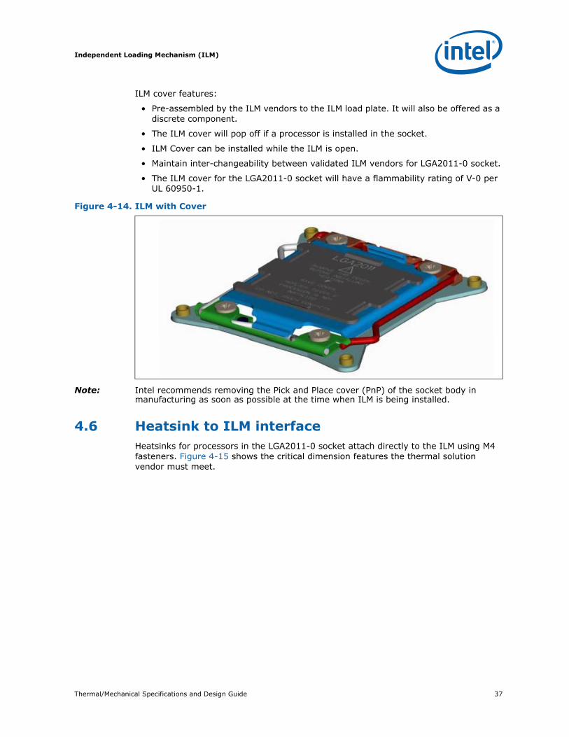
4.5 ILM CoverIntel has developed a cover that will snap on to the ILM for the LGA2011 socket family.
The ILM cover is intended to reduce the potential for socket contact damage from the operator / customer fingers being close to the socket contacts to remove or install the pick and place cover. By design the ILM cover and pick and place covers can not be installed simultaneously.
The ILM cover concept is shown in Figure 4-14.
This cover is intended to be used in place of the pick and place cover once the ILM is assembled to the board. The ILM will be offered with the ILM cover pre assembled as well as a discrete part.
Figure 4-12. Pin 1 Markings on the ILM Frame
Figure 4-13. Closing ILM and Loadplate
Thermal/Mechanical Specifications and Design Guide 37
Independent Loading Mechanism (ILM)
ILM cover features:
• Pre-assembled by the ILM vendors to the ILM load plate. It will also be offered as a discrete component.
• The ILM cover will pop off if a processor is installed in the socket.
• ILM Cover can be installed while the ILM is open.
• Maintain inter-changeability between validated ILM vendors for LGA2011-0 socket.
• The ILM cover for the LGA2011-0 socket will have a flammability rating of V-0 per UL 60950-1.
Note: Intel recommends removing the Pick and Place cover (PnP) of the socket body in manufacturing as soon as possible at the time when ILM is being installed.
4.6 Heatsink to ILM interfaceHeatsinks for processors in the LGA2011-0 socket attach directly to the ILM using M4 fasteners. Figure 4-15 shows the critical dimension features the thermal solution vendor must meet.
Figure 4-14. ILM with Cover

Independent Loading Mechanism (ILM)
38 Thermal/Mechanical Specifications and Design Guide
Note: For IHS height above board see Table 5-2.
§
Figure 4-15. Heatsink to ILM Interface
4.178 +0.38/ -0.20 See Note Below
80.00
80.00
38.00
38.00
M4x0.74 PL
Thermal/Mechanical Specifications and Design Guide 39
LGA2011-0 Socket and ILM Electrical, Mechanical, and Environmental Specifications
5 LGA2011-0 Socket and ILM Electrical, Mechanical, andEnvironmental Specifications
This chapter describes the electrical, mechanical, and environmental specifications for the LGA2011-0 socket and the Independent Loading Mechanism.
5.1 Component Mass
Note:1. This is an approximate mass.
5.2 Package/Socket Stackup HeightTable 5-2 provides the stackup height of a processor in the 2011-0-land LGA package and LGA2011-0 socket with the ILM closed and the processor fully seated in the socket.
Notes:1. This data is provided for information only, and should be derived from: (a) the height of the socket seating
plane above the motherboard after reflow, given in Appendix B, (b) the height of the package, from the package seating plane to the top of the IHS, and accounting for its nominal variation and tolerances that are given in the corresponding processor Datasheet listed in Table 1-1.
2. This value is a RSS calculation at 3 Sigma
Table 5-1. Socket and Retention Component Mass
Component Mass
Socket Body, Contacts and PnP Cover 251g
Square ILM Assembly 82g
Backplate 84g
Table 5-2. 2011-land Package and LGA2011-0 Socket Stackup Height
Integrated Stackup Height (mm)From Top of Board to Top of IHS
8.014 ±0.34 mm
LGA2011-0 Socket and ILM Electrical, Mechanical, and Environmental Specifications
40 Thermal/Mechanical Specifications and Design Guide
5.3 Loading SpecificationsThe socket will be tested against the conditions listed in Chapter 9, “Quality and Reliability Requirements” with heatsink and the ILM attached, under the loading conditions outlined in this chapter.
Table 5-3 provides load specifications for the LGA2011-0 socket with the ILM installed. The maximum limits should not be exceeded during heatsink assembly, shipping conditions, or standard use condition. Exceeding these limits during test may result in component failure. The socket body should not be used as a mechanical reference or load-bearing surface for thermal solutions.
Notes:1. These specifications apply to uniform compressive loading in a direction perpendicular to the IHS top
surface.2. This is the minimum and maximum static force that must be applied by the heatsink and its retention
solution at Beginning of Life (BOL).3. Loading limits are for the LGA2011-0 socket.4. This minimum limit defines the compressive force required to electrically seat the processor onto the socket
contacts.5. Dynamic loading is defined as an 11 ms duration average load superimposed on the static load
requirement.6. Test condition used a heatsink mass of 600gm [1.32 lb.] with 50 g acceleration measured at heatsink mass.
The dynamic portion of this specification in the product application can have flexibility in specific values, but the ultimate product of mass times acceleration should not exceed this dynamic load.
7. Conditions must be satisfied at the beginning of life (BOL) and the loading system stiffness for non-reference designs need to meet a specific stiffness range to satisfy end of life loading requirements.
8. These loading values are preliminary and subjected to change.9. End of Life (EOL) minimum heatsink static load. The methods and techniques to evaluate heat sink EOL
load are included in Appendix F.10. Beginning of Life (EOL) heat sink load. The methods and techniques to evaluate heat sink BOL load will be
included in a later release of this document.11. The maximum mass includes all components in the thermal solution. This mass limit is evaluated using the
POR heatsink attached to a PCB.12. The minimum BOL load is for guidance only. Thermal solutions must satisfy the EOL minimum load to be
compliant to the speicification.
5.4 Electrical RequirementsLGA2011-0 socket electrical requirements are measured from the socket-seating plane of the processor to the component side of the socket PCB to which it is attached. All specifications are maximum values (unless otherwise stated) for a single socket contact, but includes effects of adjacent contacts where indicated.
Table 5-3. Socket and ILM Mechanical Specifications
Parameter Min Max Notes
Static compressive load from ILM cover to processor IHS 445 N [100 lbf] 712 N [160 lbf] 3, 4, 7, 8
Heatsink Static Compressive Load BOL 222 N [50 lbf] 356 N [80 lbf] 1, 2, 3, 4, 8, 10, 12
Heatsink Static Compressive Load EOL 133 N [30 lbf] 356 N [80 lbf] 1, 3, 4, 8, 9
Dynamic Load (with heatsink installed) N/A 589 N [132 lbf] 1, 3, 5, 6, 8
Pick and Place Cover Insertion / Removal force N/A 6.2 N [1.7 lbf] 8
Load Lever actuation force N/A 31 N [7.0 lbf] in the vertical direction 8
Maximum heatsink mass N/A 600g 11
Thermal/Mechanical Specifications and Design Guide 41
LGA2011-0 Socket and ILM Electrical, Mechanical, and Environmental Specifications
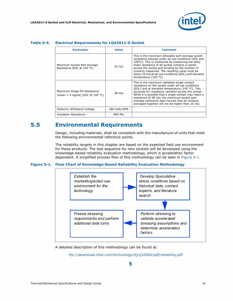
5.5 Environmental RequirementsDesign, including materials, shall be consistent with the manufacture of units that meet the following environmental reference points.
The reliability targets in this chapter are based on the expected field use environment for these products. The test sequence for new sockets will be developed using the knowledge-based reliability evaluation methodology, which is acceleration factor dependent. A simplified process flow of this methodology can be seen in Figure 5-1.
A detailed description of this methodology can be found at:
ftp://download.intel.com/technology/itj/q32000/pdf/reliability.pdf
§
Table 5-4. Electrical Requirements for LGA2011-0 Socket
Parameter Value Comment
Maximum Socket Part Average Resistance (EOL @ 100 °C) 25 mΩ
This is the maximum allowable part average socket resistance allowed under all use conditions (EOL and 100°C). This is monitored by measuring the daisy chain resistance of all socket contacts in series across the socket and dividing by the number of contacts measured. The resulting value must be below 25 mΩ at all use conditions (EOL) and elevated temperature (100 °C).
Maximum Single Pin Resistance(mean + 4 sigma) (EOL @ 100 °C)
38 mΩ
This is the maximum validated single contact resistance on the socket under all use conditions (EOL) and at elevated temperature (100 °C). This accounts for resistance variation across the socket. While it is possible that a single contact may reach a resistance of 38 mΩ, the maximum socket part average resistance spec insures that all contacts averaged together will not be higher than 25 mΩ
Dielectric Withstand Voltage 360 Volts RMS
Insulation Resistance 800 MΩ
Figure 5-1. Flow Chart of Knowledge-Based Reliability Evaluation Methodology
Establish the market/expected use environment for the technology
Develop Speculative stress conditions based on historical data, content experts, and literature search
Perform stressing to validate accelerated stressing assumptions and determine acceleration factors
Freeze stressing requirements and perform additional data turns

LGA2011-0 Socket and ILM Electrical, Mechanical, and Environmental Specifications
42 Thermal/Mechanical Specifications and Design Guide
Thermal/Mechanical Specifications and Design Guide 43
Thermal Management Specifications
6 Thermal Management Specifications
6.1 Package Thermal SpecificationsThe processor requires a thermal solution to maintain temperatures within operating limits. Any attempt to operate the processor outside these limits may result in permanent damage to the processor and potentially other components within the system. Maintaining the proper thermal environment is key to reliable, long-term system operation.
A complete solution includes both component and system level thermal management features. Component level thermal solutions can include active or passive heatsinks attached to the processor integrated heat spreader (IHS). Typical system level thermal solutions may consist of system fans combined with ducting and venting.
This section provides data necessary for developing a complete thermal solution. For more information on the reference thermal solution and designing a component level thermal solution, refer to Chapter 8.
Note: The boxed processor will ship with a component thermal solution.
6.1.1 Thermal SpecificationsTo allow optimal operation and long-term reliability of Intel processor-based systems, the processor must remain within the minimum and maximum case temperature (TCASE) specifications as defined by the applicable thermal profile. Thermal solutions not designed to provide sufficient thermal capability may affect the long-term reliability of the processor and system.
The Intel® Core™ i7-3960X, i7-3970X processor Extreme Edition, Intel® Core™ i7-3930K processor, and Intel® Core™ i7-3820 processor implement a methodology for managing processor temperatures which is intended to support acoustic noise reduction through fan speed control and to assure processor reliability. Selection of the appropriate fan speed is based on the relative temperature data reported by the processor’s Platform Environment Control Interface (PECI) as described in Section 6.3.
The temperature reported over PECI is always a negative value and represents a delta below the onset of thermal control circuit (TCC) activation, as indicated by the PROCHOT# signal. Systems that implement fan speed control must be designed to use this data.
Intel recommends that complete thermal solution designs target the Thermal Design Power (TDP). The Adaptive Thermal Monitor feature is intended to help protect the processor in the event that an application exceeds the TDP recommendation for a sustained time period. The Adaptive Thermal Monitor feature must be enabled for the processor to remain within its specifications.
Thermal Management Specifications
44 Thermal/Mechanical Specifications and Design Guide
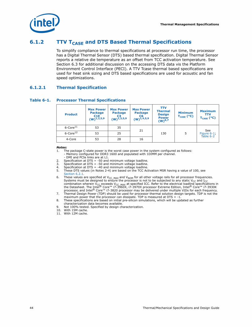
6.1.2 TTV TCASE and DTS Based Thermal SpecificationsTo simplify compliance to thermal specifications at processor run time, the processor has a Digital Thermal Sensor (DTS) based thermal specification. Digital Thermal Sensor reports a relative die temperature as an offset from TCC activation temperature. See Section 6.3 for additional discussion on the accessing DTS data vis the Platform Environment Control Interface (PECI). A TTV Tcase thermal based specifications are used for heat sink sizing and DTS based specifications are used for acoustic and fan speed optimizations.
6.1.2.1 Thermal Specification
Notes:1. The package C-state power is the worst case power in the system configured as follows:
- Memory configured for DDR3 1600 and populated with 1DIMM per channel.- DMI and PCIe links are at L1.
2. Specification at DTS = -50 and minimum voltage loadline.3. Specification at DTS = -50 and minimum voltage loadline.4. Specification at DTS = -40 and minimum voltage loadline.5. These DTS values (in Notes 2-4) are based on the TCC Activation MSR having a value of 100, see
Section 6.2.1.6. These values are specified at VCC_MAX and VNOM for all other voltage rails for all processor frequencies.
Systems must be designed to ensure the processor is not to be subjected to any static VCC and ICC combination wherein VCC exceeds VCC_MAX at specified ICC. Refer to the electrical loadline specifications in the Datasheet. The Intel® Core™ i7-3960X, i7-3970X processor Extreme Edition, Intel® Core™ i7-3930K processor, and Intel® Core™ i7-3820 processor may be delivered under multiple VIDs for each frequency.
7. Thermal Design Power (TDP) should be used for processor thermal solution design targets. TDP is not the maximum power that the processor can dissipate. TDP is measured at DTS = -1.
8. These specifications are based on initial pre-silicon simulations, which will be updated as further characterization data becomes available.
9. Not 100% tested. Specified by design characterization.10. With 15M cache.11. With 12M cache.
Table 6-1. Processor Thermal Specifications
Product
Max PowerPackage
C1E(W)1,2,5,9
Max PowerPackage
C3(W)1,3,5,9
Max Power Package
C6(W)1,4,5,9
TTV Thermal Design Power(W)6,7
MinimumTCASE (°C)
Maximum TTV
TCASE (°C)
6-Core11 53 3521
130 5See
Figure 6-1; Table 6-2
6-Core12 53 25
4-Core 53 28 16
Thermal/Mechanical Specifications and Design Guide 45
Thermal Management Specifications
Notes:1. Refer to Table 6-2 for discrete points that constitute thermal profile. 2. Refer to the Chapter 8 for system and environmental implementation details.
Figure 6-1. TTV Thermal Profile
Table 6-2. 130W TTV Thermal Profile (Sheet 1 of 2)
Power (W) Maximum TTV TCASE (°C)
Power (W) Maximum TTV TCASE (°C)
0 43.4 66 55.3
2 43.8 68 55.6
4 44.1 70 56.0
6 44.5 72 56.4
8 44.8 73 56.5
10 45.2 76 57.1
12 45.6 78 57.4
14 45.9 80 57.8
16 46.3 82 58.2
18 46.6 84 58.5
20 47.0 86 58.9
22 47.4 88 59.2
24 47.7 90 59.6
26 48.1 92 60.0
28 48.4 94 60.3
30 48.8 96 60.7
32 49.2 98 61.0
34 49.5 100 61.4
Thermal Management Specifications
46 Thermal/Mechanical Specifications and Design Guide
6.1.3 Processor Specification for Operation Where DigitalThermal Sensor Exceeds TCONTROL
When the DTS value is less than TCONTROL the fan speed control algorithm can reduce the speed of the thermal solution fan. This remains the same as with the previous guidance for fan speed control.
During operation, when the DTS value is greater than TCONTROL, the fan speed control algorithm must drive the fan speed to meet or exceed the target thermal solution performance (ΨCA) shown in Table 6-3 for the Intel® Core™ i7-3960X, i7-3970X processor Extreme Edition, Intel® Core™ i7-3930K processor, and Intel® Core™ i7-3820 processor. To get the full acoustic benefit of the DTS specification, ambient temperature monitoring is necessary.
36 49.9 102 61.8
38 50.2 104 62.1
40 50.6 106 62.5
42 51.0 108 62.8
44 51.3 110 63.2
46 51.7 112 63.6
48 52.0 114 63.9
50 52.4 116 64.3
52 52.8 118 64.6
54 53.1 120 65.0
56 53.5 122 65.4
58 53.8 124 65.7
60 54.2 126 66.1
62 54.6 128 66.4
64 54.9 130 66.8
Table 6-2. 130W TTV Thermal Profile (Sheet 2 of 2)
Power (W) Maximum TTV TCASE (°C)
Power (W) Maximum TTV TCASE (°C)
Table 6-3. Thermal Solution Performance above TCONTROL for the Intel® Core™ i7-3960X, i7-3970X Processor Extreme Edition, Intel® Core™ i7-3930K Processor, and Intel® Core™ i7-3820 Processor (Sheet 1 of 2)
TAMBIENT1 ΨCA at
DTS = TCONTROL2
ΨCA at DTS = -13
43.4 0.180 0.180
42.0 0.198 0.191
41.0 0.211 0.198
40.0 0.224 0.206
39.0 0.237 0.214
38.0 0.250 0.222
37.0 0.263 0.229
36.0 0.276 0.237
35.0 0.290 0.245
34.0 0.303 0.252
33.0 0.316 0.260
32.0 0.329 0.268
31.0 0.342 0.275
30.0 0.355 0.283

Thermal/Mechanical Specifications and Design Guide 47
Thermal Management Specifications
1. The ambient temperature is measured at the inlet to the processor thermal solution.2. This column can be expressed as a function of TAMBIENT by the following equation:
YCA = 0.18 + (43.4 - TAMBIENT) x 0.0133. This column can be expressed as a function of TAMBIENT by the following equation:
YCA = 0.18 + (43.4 - TAMBIENT) x 0.0077
6.1.4 Thermal MetrologyThe maximum TTV case temperatures (TCASE-MAX) specified in Table 6-2 is measured at the geometric top center of the TTV integrated heat spreader (IHS). Figure 6-2 illustrates the location where TCASE temperature measurements should be made. A dimensioned drawing for milling the groove to place the thermocouple on the IHS can be found in Appendix E.
29.0 0.368 0.291
28.0 0.381 0.298
27.0 0.394 0.306
26.0 0.407 0.314
25.0 0.420 0.322
24.0 0.433 0.329
23.0 0.446 0.337
22.0 0.459 0.345
21.0 0.472 0.352
20.0 0.485 0.360
19.0 0.498 0.368
18.0 0.511 0.375
Table 6-3. Thermal Solution Performance above TCONTROL for the Intel® Core™ i7-3960X, i7-3970X Processor Extreme Edition, Intel® Core™ i7-3930K Processor, and Intel® Core™ i7-3820 Processor (Sheet 2 of 2)
TAMBIENT1 ΨCA at
DTS = TCONTROL2
ΨCA at DTS = -13
Figure 6-2. Case Temperature (TCASE) Measurement Location
52.5
45.0
Pin 1
Measure Tcase at the Geometric
Center of the Package

Thermal Management Specifications
48 Thermal/Mechanical Specifications and Design Guide
6.2 Processor Core Thermal Features
6.2.1 Processor TemperatureA feature in the processor is a software readable field in the IA32_TEMPERATURE_TARGET register that contains the minimum temperature at which the TCC will be activated and PROCHOT_N will be asserted. The TCC activation temperature is calibrated on a part-by-part basis and normal factory variation may result in the actual TCC activation temperature being higher than the value listed in the register. TCC activation temperatures may change based on processor stepping, frequency or manufacturing efficiencies.
6.2.2 Adaptive Thermal MonitorThe Adaptive Thermal Monitor feature provides an enhanced method for controlling the processor temperature when the processor silicon reaches its maximum operating temperature. Adaptive Thermal Monitor uses Thermal Control Circuit (TCC) activation to reduce processor power using a combination of methods. The first method (Frequency/SVID control) involves the processor adjusting its operating frequency (using the core ratio multiplier) and input voltage (using the SVID signals). This combination of reduced frequency and voltage results in a reduction to the processor power consumption. The second method (clock modulation) reduces power consumption by modulating (starting and stopping) the internal processor core clocks. The processor intelligently selects the appropriate TCC method to use on a dynamic basis. BIOS is not required to select a specific method (as with previous-generation processors supporting TM1 or TM2).
The Adaptive Thermal Monitor feature must be enabled for the processor to be operating within specifications. The temperature at which Adaptive Thermal Monitor activates the Thermal Control Circuit is not user configurable and is not software visible. Snooping and interrupt processing are performed in the normal manner while the TCC is active.
With a properly designed and characterized thermal solution, it is anticipated that the TCC would be activated for very short periods of time when running the most power intensive applications. The processor performance impact due to these brief periods of TCC activation is expected to be so minor that it would be immeasurable. An under-designed thermal solution that is not able to prevent excessive activation of the TCC in the anticipated ambient environment may cause a noticeable performance loss, and in some cases may result in a TC that exceeds the specified maximum temperature which may affect the long-term reliability of the processor. In addition, a thermal solution that is significantly under-designed may not be capable of cooling the processor even when the TCC is active continuously. Refer to the Chapter 8 for information on designing a compliant thermal solution.
The duty cycle for the TCC, when activated by the Thermal Monitor, is factory configured and cannot be modified. The Thermal Monitor does not require any additional hardware, software drivers, or interrupt handling routines.
Thermal/Mechanical Specifications and Design Guide 49
Thermal Management Specifications
6.2.2.1 Frequency/SVID Control
The processor uses Frequency/SVID control whereby TCC activation causes the processor to adjust its operating frequency (using the core ratio multiplier) and input voltage (using the SVID signals). This combination of reduced frequency and voltage results in a reduction to the processor power consumption.
This method includes multiple operating points, each consisting of a specific operating frequency and voltage. The first operating point represents the normal operating condition for the processor. The remaining points consist of both lower operating frequencies and voltages. When the TCC is activated, the processor automatically transitions to the new lower operating frequency. This transition occurs very rapidly (on the order of microseconds). Once the new operating frequency is engaged, the processor will transition to the new core operating voltage by issuing a new SVID code to the voltage regulator. The voltage regulator must support dynamic SVID steps to support this method. During the voltage change, it will be necessary to transition through multiple SVID codes to reach the target operating voltage. Each step will be one SVID table entry (see Voltage Identification Definition in the Datasheet). The processor continues to execute instructions during the voltage transition. Operation at the lower voltages reduces the power consumption of the processor.
A small amount of hysteresis has been included to prevent rapid active/inactive transitions of the TCC when the processor temperature is near its maximum operating temperature. Once the temperature has dropped below the maximum operating temperature, and the hysteresis timer has expired, the operating frequency and voltage transition back to the normal system operating point using the intermediate SVID/frequency points. Transition of the SVID code will occur first, to insure proper operation once the processor reaches its normal operating frequency. Refer to Figure 6-3 for an illustration of this ordering.
Figure 6-3. Frequency and Voltage Ordering
Temperature
fMAX
f1f2
VIDfMAX
VID
Frequency
VIDf2
VIDf1
PROCHOT#
Time
Temperature
fMAX
f1f2
VIDfMAX
VID
Frequency
VIDf2
VIDf1
PROCHOT#
Time
Thermal Management Specifications
50 Thermal/Mechanical Specifications and Design Guide
6.2.2.2 Clock Modulation
Clock modulation is performed by alternately turning the clocks off and on at a duty cycle specific to the processor (factory configured to 37.5% on and 62.5% off for TM1). The period of the duty cycle is configured to 32 microseconds when the TCC is active. Cycle times are independent of processor frequency. A small amount of hysteresis has been included to prevent rapid active/inactive transitions of the TCC when the processor temperature is near its maximum operating temperature. Once the temperature has dropped below the maximum operating temperature, and the hysteresis timer has expired, the TCC goes inactive and clock modulation ceases. Clock modulation is automatically engaged as part of the TCC activation when the Frequency/SVID targets are at their minimum settings. It may also be initiated by software at a configurable duty cycle.
6.2.3 On-Demand ModeThe processor provides an auxiliary mechanism that allows system software to force the processor to reduce its power consumption. This mechanism is referred to as “On-Demand” mode and is distinct from the Adaptive Thermal Monitor feature. On-Demand mode is intended as a means to reduce system level power consumption. Systems must not rely on software usage of this mechanism to limit the processor temperature. If bit 4 of the IA32_CLOCK_MODULATION MSR is set to a ‘1’, the processor will immediately reduce its power consumption using modulation (starting and stopping) of the internal core clock, independent of the processor temperature. When using On-Demand mode, the duty cycle of the clock modulation is programmable using bits 3:0 of the same IA32_CLOCK_MODULATION MSR. In On-Demand mode, the duty cycle can be programmed from 6.25% on / 93.75% off to 93.75% on / 6.25% off in 6.25% increments. On-Demand mode may be used in conjunction with the Adaptive Thermal Monitor; however, if the system tries to enable On-Demand mode at the same time the TCC is engaged, the factory configured duty cycle of the TCC will override the duty cycle selected by the On-Demand mode.
6.2.4 PROCHOT_N SignalAn external signal, PROCHOT_N (processor hot), is asserted when the processor core temperature has reached its maximum operating temperature. If Adaptive Thermal Monitor is enabled (note it must be enabled for the processor to be operating within specification), the TCC will be active when PROCHOT_N is asserted.
The PROCHOT_N signal is bi-directional in that it can either signal when the processor (any core) has reached its maximum operating temperature or be driven from an external source to activate the TCC. The ability to activate the TCC using PROCHOT_N can provide a means for thermal protection of system components.
As an output, PROCHOT_N will go active when the processor temperature monitoring sensor detects that one or more cores has reached its maximum safe operating temperature. This indicates that the processor Thermal Control Circuit (TCC) has been activated, if enabled. As an input, assertion of PROCHOT_N by the system will activate the TCC, if enabled, for all cores. TCC activation due to PROCHOT_N assertion by the system will result in the processor immediately transitioning to the minimum frequency and corresponding voltage (using Freq/SVID control). Clock modulation is not activated in this case. The TCC will remain active until the system de-asserts PROCHOT_N.
PROCHOT_N can allow voltage regulator (VR) thermal designs to target maximum sustained current instead of maximum current. Systems should still provide proper cooling for the VR, and rely on PROCHOT_N as a backup in case of system cooling

Thermal/Mechanical Specifications and Design Guide 51
Thermal Management Specifications
failure. The system thermal design should allow the power delivery circuitry to operate within its temperature specification even while the processor is operating at its Thermal Design Power.
With a properly designed and characterized thermal solution, it is anticipated that PROCHOT_N will be asserted for very short periods of time when running the most power intensive applications. An under-designed thermal solution that is not able to prevent excessive assertion of PROCHOT_N in the anticipated ambient environment may cause a noticeable performance loss. Refer to the appropriate platform design guide and for details on implementing the bi-directional PROCHOT_N feature.
6.2.5 THERMTRIP_N SignalRegardless of whether Adaptive Thermal Monitor is enabled, in the event of a catastrophic cooling failure, the processor will automatically shut down when the silicon has reached an elevated temperature (refer to the THERMTRIP_N definition in the Datasheet). At this point, the THERMTRIP_N signal will go active and stay active. THERMTRIP_N activation is independent of processor activity. If THERMTRIP_N is asserted, all processor supplies (VCC, VTTA, VTTD, VSA, VCCPLL, VCCD) must be removed within the timeframe which is TBD at this point. The temperature at which THERMTRIP_N asserts is not user configurable and is not software visible.
6.3 Platform Environment Control Interface (PECI)
6.3.1 IntroductionPECI uses a single wire for self-clocking and data transfer. The bus requires no additional control lines. The physical layer is a self-clocked one-wire bus that begins each bit with a driven, rising edge from an idle level near zero volts. The duration of the signal driven high depends on whether the bit value is a logic ‘0’ or logic ‘1’. PECI also includes variable data transfer rate established with every message. In this way, it is highly flexible even though underlying logic is simple.
The interface design was optimized for interfacing to Intel processor and chipset components in both single processor and multiple processor environments. The single wire interface provides low board routing overhead for the multiple load connections in the congested routing area near the processor and chipset components. Bus speed, error checking, and low protocol overhead provides adequate link bandwidth and reliability to transfer critical device operating conditions and configuration information.
The PECI bus offers:
• A wide speed range from 2 Kbps to 2 Mbps
• CRC check byte used to efficiently and atomically confirm accurate data delivery
• Synchronization at the beginning of every message minimizes device timing accuracy requirements.
Thermal Management Specifications
52 Thermal/Mechanical Specifications and Design Guide
For desktop and single processor server and workstation processors system temperature monitoring and fan speed control management purpose, the PECI 3.0 commands that are commonly implemented includes:
• Ping()
• GetDIB()
• GetTemp()
• RdPkgConfig() to get:
— IA32_TEMPERATURE_TARGET MSR— TCONTROL
— TDP
See the Chapter 7 for the PECI command details.
6.3.2 PECI Client CapabilitiesThe Intel® Core™ i7-3960X, i7-3970X processor Extreme Edition, Intel® Core™ i7-3930K processor, and Intel® Core™ i7-3820 processor support the following sideband functions:
• Processor and DRAM thermal management
• Platform manageability functions including thermal, power and electrical error monitoring
See the Chapter 7 for the PECI command details.
6.4 Fan Speed Control with Digital Thermal Sensor Processor fan speed control is managed by comparing DTS temperature data against the processor-specific value stored in the static variable, TCONTROL. When the DTS temperature data is less than TCONTROL, the fan speed control algorithm can reduce the speed of the thermal solution fan. This remains the same as with the previous guidance for fan speed control. Refer to Section 6.1.3 for guidance where the DTS temperature data exceeds TCONTROL.
The DTS temperature data is delivered over PECI, in response to a GetTemp() command, and reported as a relative value to TCC activation target. The temperature data reported over PECI is always a negative value and represents a delta below the onset of thermal control circuit (TCC) activation, as indicated by the PROCHOT# signal. Therefore, as the temperature approaches TCC activation, the value approaches zero degrees.
§
Thermal/Mechanical Specifications and Design Guide 53
PECI Interface
7 PECI Interface
7.1 Platform Environment Control Interface (PECI)The Platform Environment Control Interface (PECI) uses a single wire for self-clocking and data transfer. The bus requires no additional control lines. The physical layer is a self-clocked one-wire bus that begins each bit with a driven, rising edge from an idle level near zero volts. The duration of the signal driven high depends on whether the bit value is a logic ‘0’ or logic ‘1’. PECI also includes variable data transfer rate established with every message. In this way, it is highly flexible even though underlying logic is simple.
The interface design was optimized for interfacing to Intel processor and chipset components in both single processor and multiple processor environments. The single wire interface provides low board routing overhead for the multiple load connections in the congested routing area near the processor and chipset components. Bus speed, error checking, and low protocol overhead provides adequate link bandwidth and reliability to transfer critical device operating conditions and configuration information.
The PECI bus offers:• A wide speed range from 2 Kbps to 2 Mbps• CRC check byte used to efficiently and atomically confirm accurate data delivery• Synchronization at the beginning of every message minimizes device timing
accuracy requirements
Generic PECI specification details are out of the scope of this document. What follows is a processor-specific PECI client definition, and is largely an addendum to the PECI Network Layer and Design Recommendations sections for the PECI specification.
Note: The PECI commands described in this document apply primarily to the Intel® Core™ i7-3960X, i7-3970X processor Extreme Edition, Intel® Core™ i7-3930K processor, and Intel® Core™ i7-3820 processor. The these processors utilizes the capabilities described in this document to indicate support for four memory channels. Refer to Table 7-1 for the list of PECI commands supported by the Intel® Core™ i7-3960X, i7-3970X processor Extreme Edition, Intel® Core™ i7-3930K processor, and Intel® Core™ i7-3820 processor.
Table 7-1. Summary of Processor-specific PECI Commands
Command
Supported on Intel® Core™ i7-3960X, i7-3970X Processor
Extreme Edition, Intel® Core™ i7-3930K Processor, and Intel® Core™ i7-3820
Processor
Ping() YesGetDIB() Yes
GetTemp() YesRdPkgConfig() YesWrPkgConfig() Yes
RdIAMSR() YesWrIAMSR() No
RdPCIConfig() YesWrPCIConfig() No
RdPCIConfigLocal() YesWrPCIConfigLocal() Yes

PECI Interface
54 Thermal/Mechanical Specifications and Design Guide
7.1.1 PECI Client CapabilitiesThe processor PECI client is designed to support the following sideband functions:
• Processor and DRAM thermal management
• Platform manageability functions including thermal, power, and error monitoring
• Processor interface tuning and diagnostics capabilities (Intel Interconnect BIST).
7.1.1.1 Thermal Management
Processor fan speed control is managed by comparing Digital Thermal Sensor (DTS) thermal readings acquired usingPECI against the processor-specific fan speed control reference point, or TCONTROL. Both TCONTROL and DTS thermal readings are accessible using the processor PECI client. These variables are referenced to a common temperature, the TCC activation point, and are both defined as negative offsets from that reference.
PECI-based access to the processor package configuration space provides a means for Super IO (SIO) or other platform management devices to actively manage the processor, memory power and thermal features. Details on the list of available power and thermal optimization services can be found in Section 7.1.2.6.
7.1.1.2 Platform Manageability
PECI allows read access to certain error and status monitoring registers within the processor It also provides insight into thermal monitoring functions such as TCC activation timers and thermal error logs as covered in Section 7.1.2.6.
7.1.1.3 Processor Interface Tuning and Diagnostics
Intel® Core™ i7-3960X, i7-3970X processor Extreme Edition, Intel® Core™ i7-3930K processor, and Intel® Core™ i7-3820 processor Intel Interconnect Built-In Self Test (Intel IBIST) allows for in-field diagnostic capabilities in memory controller interfaces. PECI provides a port to execute these diagnostics using its PCI Configuration read and write capabilities.
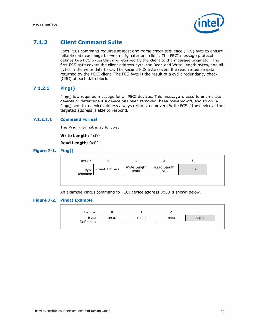
Thermal/Mechanical Specifications and Design Guide 55
PECI Interface
7.1.2 Client Command SuiteEach PECI command requires at least one frame check sequence (FCS) byte to ensure reliable data exchange between originator and client. The PECI message protocol defines two FCS bytes that are returned by the client to the message originator. The first FCS byte covers the client address byte, the Read and Write Length bytes, and all bytes in the write data block. The second FCS byte covers the read response data returned by the PECI client. The FCS byte is the result of a cyclic redundancy check (CRC) of each data block.
7.1.2.1 Ping()
Ping() is a required message for all PECI devices. This message is used to enumerate devices or determine if a device has been removed, been powered-off, and so on. A Ping() sent to a device address always returns a non-zero Write FCS if the device at the targeted address is able to respond.
7.1.2.1.1 Command Format
The Ping() format is as follows:
Write Length: 0x00
Read Length: 0x00
An example Ping() command to PECI device address 0x30 is shown below.
Figure 7-1. Ping()
Byte #
Byte Definition
0
Client Address
1
Write Length0x00
2
Read Length0x00
3
FCS
Figure 7-2. Ping() Example
Byte #
Byte Definition
0
0x30
1
0x00
2
0x00
3
0xe1

PECI Interface
56 Thermal/Mechanical Specifications and Design Guide
7.1.2.2 GetDIB()
The processor PECI client implementation of GetDIB() includes an 8-byte response and provides information regarding client revision number and the number of supported domains. All processor PECI clients support the GetDIB() command.
7.1.2.2.1 Command Format
The GetDIB() format is as follows:
Write Length: 0x01
Read Length: 0x08
Command: 0xF7
7.1.2.2.2 Device Info
The Device Info byte gives details regarding the PECI client configuration. At a minimum, all clients supporting GetDIB will return the number of domains inside the package using this field. With any client, at least one domain (Domain 0) must exist. Therefore, the Number of Domains reported is defined as the number of domains in addition to Domain 0. For example, if bit 2 of the Device Info byte returns a ‘1’, that would indicate that the PECI client supports two domains.
Figure 7-3. GetDIB()
Byte #
Byte Definition
0
Client Address
1
Write Length0x01
2
Read Length0x08
4
FCS
3
Cmd Code0xf7
5
Device Info
6
Revision Number
7
Reserved
8
Reserved
9
Reserved
10
Reserved
11
Reserved
12
Reserved
13
FCS
Figure 7-4. Device Info Field Definition
Reserved# of Domains
Reserved
7 6 5 4 3 2 1 0
Byte# 5

Thermal/Mechanical Specifications and Design Guide 57
PECI Interface
7.1.2.2.3 Revision Number
All clients that support the GetDIB command also support Revision Number reporting. The revision number may be used by a host or originator to manage different command suites or response codes from the client. Revision Number is always reported in the second byte of the GetDIB() response. The ‘Major Revision’ number in Figure 7-5 always maps to the revision number of the PECI specification that the PECI client processor is designed to. The ‘Minor Revision’ number value depends on the exact command suite supported by the PECI client as defined in Table 7-2.
Figure 7-5. Revision Number Definition
Table 7-2. Minor Revision Number Meaning
Revision Field, Minor
Revision Bits [3:0]
Supported Features
0x0 Ping(), GetDIB(), Gettemp()
0x1 Ping(), GetDIB(), Gettemp(), RdPkgConfig(), WrPkg Config()
0x2 Ping(), GetDIB(), Gettemp(), RdPkgConfig(), WrPkg Config(), RdIAMSR()
0x3Ping(), GetDIB(), Gettemp(), RdPkgConfig(), WrPkg Config(), RdIAMSR(), RdPCIconfigLocal(), WrPCIconfigLocal()
0x4Ping(), GetDIB(), Gettemp(), RdPkgConfig(), WrPkg Config(), RdIAMSR(), RdPCIconfigLocal(), WrPCIconfigLocal(), RdPCIConfig()
0x5Ping(), GetDIB(), Gettemp(), RdPkgConfig(), WrPkg Config(), RdIAMSR(), RdPCIconfigLocal(), WrPCIconfigLocal(), RdPCIConfig(), WrPCIConfig()
0x6Ping(), GetDIB(), Gettemp(), RdPkgConfig(), WrPkg Config(), RdIAMSR(), RdPCIconfigLocal(), WrPCIconfigLocal(), RdPCIConfig(), WrPCIConfig(), WrIAMSR()
0347
Major Revision#Minor Revision#
Byte# 6

PECI Interface
58 Thermal/Mechanical Specifications and Design Guide
7.1.2.3 GetTemp()
The GetTemp() command is used to retrieve the maximum die temperature from a target PECI address. The temperature is used by the external thermal management system to regulate the temperature on the die. The data is returned as a negative value representing the number of degrees centigrade below the maximum processor junction temperature (Tjmax). Note that the maximum PECI temperature value of zero corresponds to the processor Tjmax. This also represents the default temperature at which the processor Thermal Control Circuit activates. The actual value that the thermal management system uses as a control set point (TCONTROL) is also defined as a negative number below Tjmax. TCONTROL may be extracted from the processor by issuing a PECI RdPkgConfig() command as described in Section 7.1.2.4 or using a RDMSR instruction. TCONTROL application to fan speed control management is defined in Chapter 6. Refer to Section 7.1.9 for details regarding PECI temperature data formatting.
7.1.2.3.1 Command Format
The GetTemp() format is as follows:
Write Length: 0x01
Read Length: 0x02
Command: 0x01
Description: Returns the highest die temperature for addressed processor PECI client.
Example bus transaction for a thermal sensor device located at address 0x30 returning a value of negative 10 counts is show in Figure 7-7.
Figure 7-6. GetTemp()
Byte #
Byte Definition
0
Client Address
1
Write Length0x01
2
Read Length0x02
4
FCS
5
Temp[7:0]
6
Temp[15:8]
7
FCS
3
Cmd Code0x01
Figure 7-7. GetTemp() Example
Byte #
Byte Definition
0
0x30
1
0x01
2
0x02
4
0xef
5
0x80
6
0xfd
7
0x4b
3
0x01
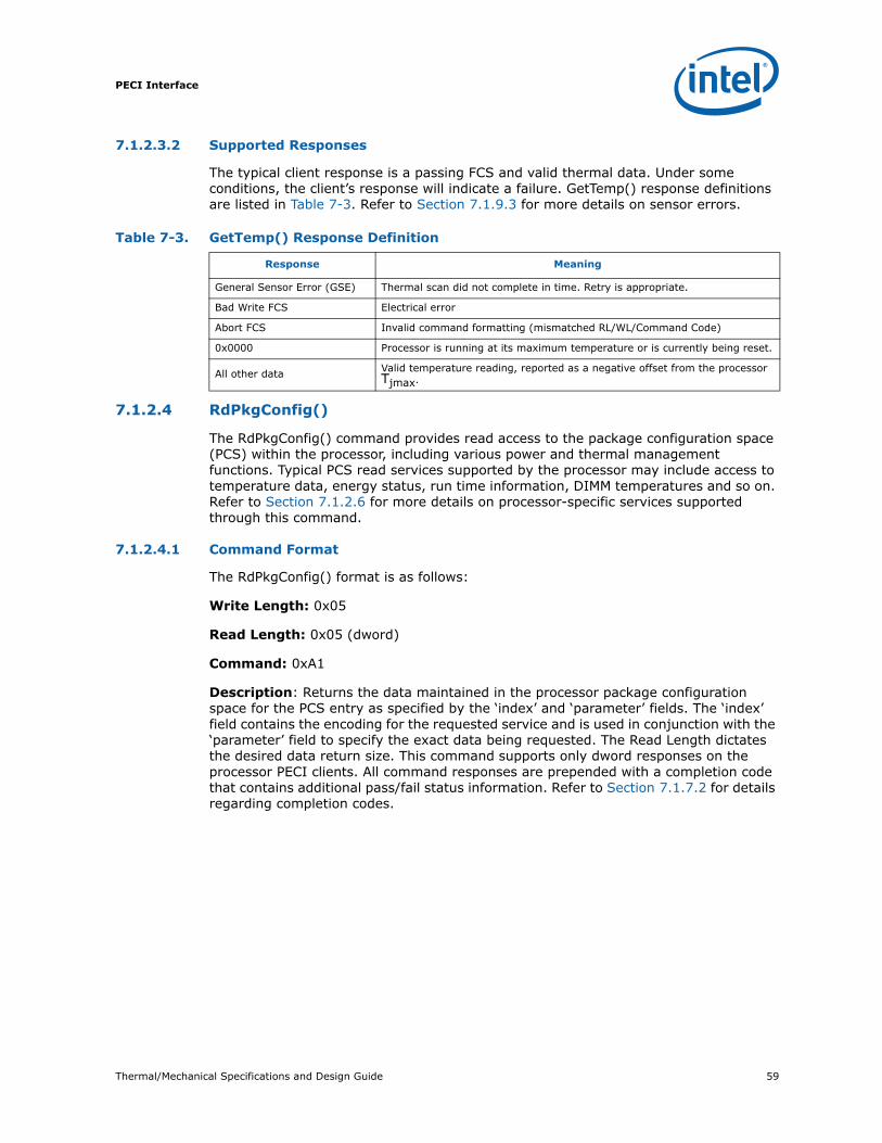
Thermal/Mechanical Specifications and Design Guide 59
PECI Interface
7.1.2.3.2 Supported Responses
The typical client response is a passing FCS and valid thermal data. Under some conditions, the client’s response will indicate a failure. GetTemp() response definitions are listed in Table 7-3. Refer to Section 7.1.9.3 for more details on sensor errors.
7.1.2.4 RdPkgConfig()
The RdPkgConfig() command provides read access to the package configuration space (PCS) within the processor, including various power and thermal management functions. Typical PCS read services supported by the processor may include access to temperature data, energy status, run time information, DIMM temperatures and so on. Refer to Section 7.1.2.6 for more details on processor-specific services supported through this command.
7.1.2.4.1 Command Format
The RdPkgConfig() format is as follows:
Write Length: 0x05
Read Length: 0x05 (dword)
Command: 0xA1
Description: Returns the data maintained in the processor package configuration space for the PCS entry as specified by the ‘index’ and ‘parameter’ fields. The ‘index’ field contains the encoding for the requested service and is used in conjunction with the ‘parameter’ field to specify the exact data being requested. The Read Length dictates the desired data return size. This command supports only dword responses on the processor PECI clients. All command responses are prepended with a completion code that contains additional pass/fail status information. Refer to Section 7.1.7.2 for details regarding completion codes.
Table 7-3. GetTemp() Response Definition
Response Meaning
General Sensor Error (GSE) Thermal scan did not complete in time. Retry is appropriate.
Bad Write FCS Electrical error
Abort FCS Invalid command formatting (mismatched RL/WL/Command Code)
0x0000 Processor is running at its maximum temperature or is currently being reset.
All other data Valid temperature reading, reported as a negative offset from the processor Tjmax.
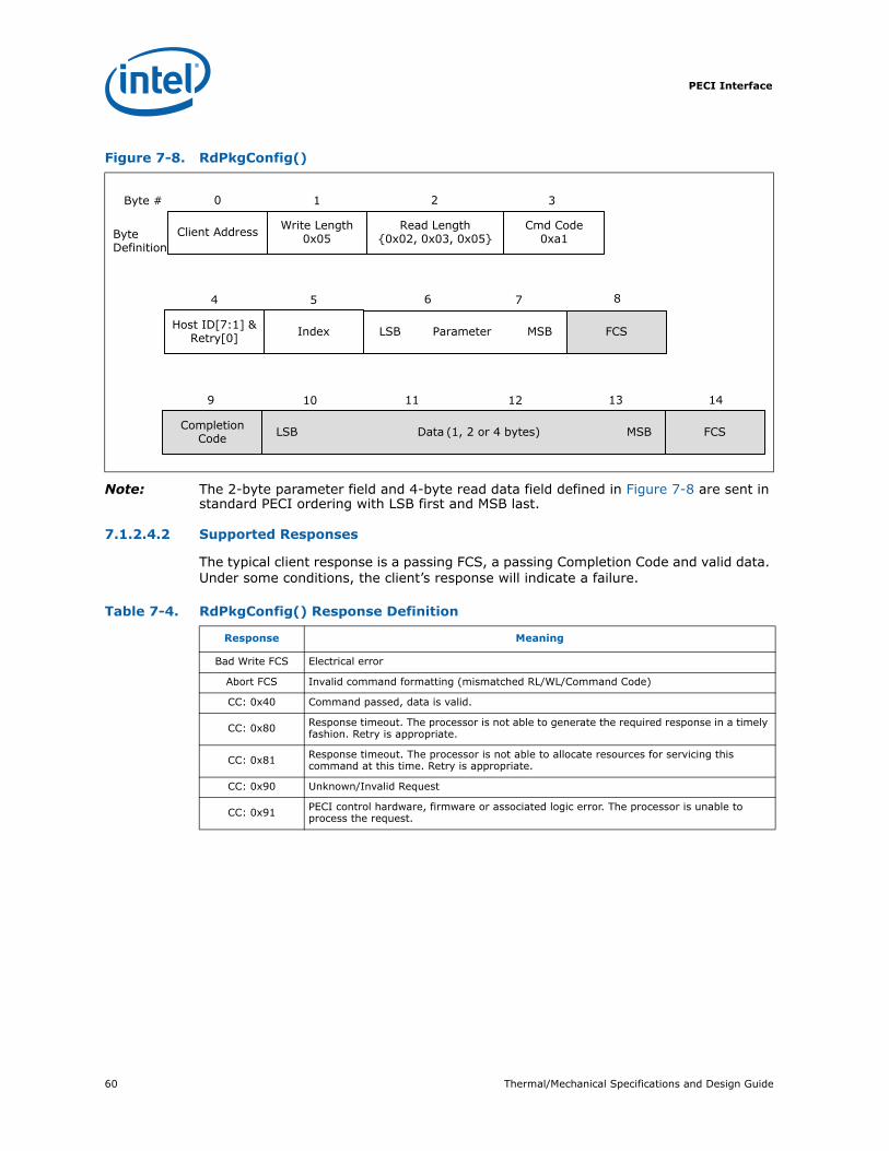
PECI Interface
60 Thermal/Mechanical Specifications and Design Guide
Note: The 2-byte parameter field and 4-byte read data field defined in Figure 7-8 are sent in standard PECI ordering with LSB first and MSB last.
7.1.2.4.2 Supported Responses
The typical client response is a passing FCS, a passing Completion Code and valid data. Under some conditions, the client’s response will indicate a failure.
Figure 7-8. RdPkgConfig()
1 3
Byte Definition
Byte # 0 2
13
Index LSB Parameter MSB
10
Host ID[7:1] & Retry[0]
11
Read Length {0x02, 0x03, 0x05}
87
Cmd Code0xa1
6
12
FCS
Client Address
CompletionCode
5
LSB Data (1, 2 or 4 bytes) MSB
4
14
Write Length0x05
9
FCS
Table 7-4. RdPkgConfig() Response Definition
Response Meaning
Bad Write FCS Electrical error
Abort FCS Invalid command formatting (mismatched RL/WL/Command Code)
CC: 0x40 Command passed, data is valid.
CC: 0x80 Response timeout. The processor is not able to generate the required response in a timely fashion. Retry is appropriate.
CC: 0x81 Response timeout. The processor is not able to allocate resources for servicing this command at this time. Retry is appropriate.
CC: 0x90 Unknown/Invalid Request
CC: 0x91 PECI control hardware, firmware or associated logic error. The processor is unable to process the request.

Thermal/Mechanical Specifications and Design Guide 61
PECI Interface
7.1.2.5 WrPkgConfig()
The WrPkgConfig() command provides write access to the package configuration space (PCS) within the processor, including various power and thermal management functions. Typical PCS write services supported by the processor may include power limiting, thermal averaging constant programming and so on. Refer to Section 7.1.2.6 for more details on processor-specific services supported through this command.
7.1.2.5.1 Command Format
The WrPkgConfig() format is as follows:
Write Length: 0x0ARead Length: 0x01Command: 0xA5
AW FCS Support: Yes
Description: Writes data to the processor PCS entry as specified by the ‘index’ and ‘parameter’ fields. This command supports only dword data writes on the processor PECI clients. All command responses include a completion code that provides additional pass/fail status information. Refer to Section 7.1.7.2 for details regarding completion codes.
Note that the Assured Write FCS (AW FCS) support provides the processor client a high degree of confidence that the data it received from the host is correct. This is especially critical where the consumption of bad data might result in improper or non-recoverable operation.
The 2-byte parameter field and 4-byte write data field defined in Figure 7-9 are sent in standard PECI ordering with LSB first and MSB last.
Figure 7-9. WrPkgConfig()
1 3
Byte Definition
Read Length 0x01
Byte #
Cmd Code0xa5Client Address
0
Write Length{0x07, 0x08, 0x0a}
2
5 7
LSB Parameter MSBHost ID[7:1] & Retry[0]
4
Index
6
13
CompletionCode
12
FCS
14 15
9 11
LSB Data (1, 2 or 4 bytes) MSB
8 10
FCSAW FCS

PECI Interface
62 Thermal/Mechanical Specifications and Design Guide
7.1.2.5.2 Supported Responses
The typical client response is a passing FCS, a passing Completion Code and valid data. Under some conditions, the client’s response will indicate a failure.
7.1.2.6 Package Configuration Capabilities
Table 7-6 combines both read and write services. Any service listed as a “read” would use the RdPkgConfig() command and a service listed as a “write” would use the WrPkgConfig() command. Note that PECI requests for memory temperature or other data generated outside the processor package do not trigger special polling cycles on the processor memory or SMBus interfaces to procure the required information.
7.1.2.6.1 DRAM Thermal and Power Optimization Capabilities
DRAM thermal and power optimization services provide a way for platform thermal management solutions to program and access DRAM power, energy and temperature parameters. Memory temperature information is typically used to regulate fan speeds, tune refresh rates and throttle the memory subsystem as appropriate. Memory temperature data may be derived from a variety of sources including on-die or on-board DIMM sensors, DRAM activity information or a combination of the two. Though memory temperature data is a byte long, range of actual temperature values are determined by the DIMM specifications and operating range.
Note: The DRAM related PECI services described in this section apply only to the memory connected through the SMBus to the specific processor PECI client in question and not the overall platform memory in general.
Table 7-5. WrPkgConfig() Response Definition
Response Meaning
Bad Write FCS Electrical error or AW FCS failure
Abort FCS Invalid command formatting (mismatched RL/WL/Command Code)
CC: 0x40 Command passed, data is valid.
CC: 0x80 Response timeout. The processor was not able to generate the required response in a timely fashion. Retry is appropriate.
CC: 0x81 Response timeout. The processor is not able to allocate resources for servicing this command at this time. Retry is appropriate.
CC: 0x90 Unknown/Invalid Request
CC: 0x91 PECI control hardware, firmware or associated logic error. The processor is unable to process the request.
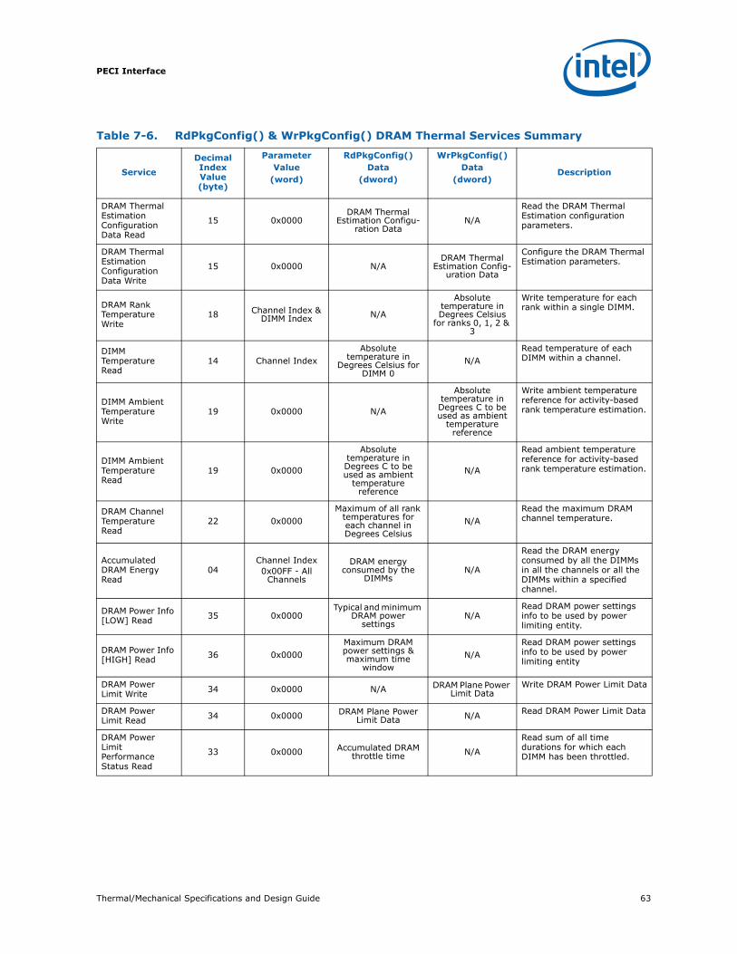
Thermal/Mechanical Specifications and Design Guide 63
PECI Interface
Table 7-6. RdPkgConfig() & WrPkgConfig() DRAM Thermal Services Summary
Service
DecimalIndex Value(byte)
Parameter Value
(word)
RdPkgConfig()Data
(dword)
WrPkgConfig()Data
(dword)Description
DRAM Thermal Estimation Configuration Data Read
15 0x0000DRAM Thermal
Estimation Configu-ration Data
N/A
Read the DRAM Thermal Estimation configuration parameters.
DRAM Thermal Estimation Configuration Data Write
15 0x0000 N/ADRAM Thermal
Estimation Config-uration Data
Configure the DRAM Thermal Estimation parameters.
DRAM Rank Temperature Write
18 Channel Index & DIMM Index N/A
Absolute temperature in Degrees Celsius
for ranks 0, 1, 2 & 3
Write temperature for each rank within a single DIMM.
DIMM Temperature Read
14 Channel IndexAbsolute
temperature in Degrees Celsius for
DIMM 0N/A
Read temperature of each DIMM within a channel.
DIMM Ambient Temperature Write
19 0x0000 N/A
Absolute temperature in Degrees C to be used as ambient
temperature reference
Write ambient temperature reference for activity-based rank temperature estimation.
DIMM Ambient Temperature Read
19 0x0000
Absolute temperature in Degrees C to be used as ambient
temperature reference
N/A
Read ambient temperature reference for activity-based rank temperature estimation.
DRAM Channel Temperature Read
22 0x0000Maximum of all rank
temperatures for each channel in Degrees Celsius
N/ARead the maximum DRAM channel temperature.
Accumulated DRAM Energy Read
04Channel Index0x00FF - All
Channels
DRAM energy consumed by the
DIMMsN/A
Read the DRAM energy consumed by all the DIMMs in all the channels or all the DIMMs within a specified channel.
DRAM Power Info [LOW] Read 35 0x0000
Typical and minimum DRAM power
settingsN/A
Read DRAM power settings info to be used by power limiting entity.
DRAM Power Info [HIGH] Read 36 0x0000
Maximum DRAM power settings & maximum time
windowN/A
Read DRAM power settings info to be used by power limiting entity
DRAM Power Limit Write 34 0x0000 N/A DRAM Plane Power
Limit DataWrite DRAM Power Limit Data
DRAM Power Limit Read 34 0x0000 DRAM Plane Power
Limit Data N/A Read DRAM Power Limit Data
DRAM Power Limit Performance Status Read
33 0x0000 Accumulated DRAM throttle time N/A
Read sum of all time durations for which each DIMM has been throttled.
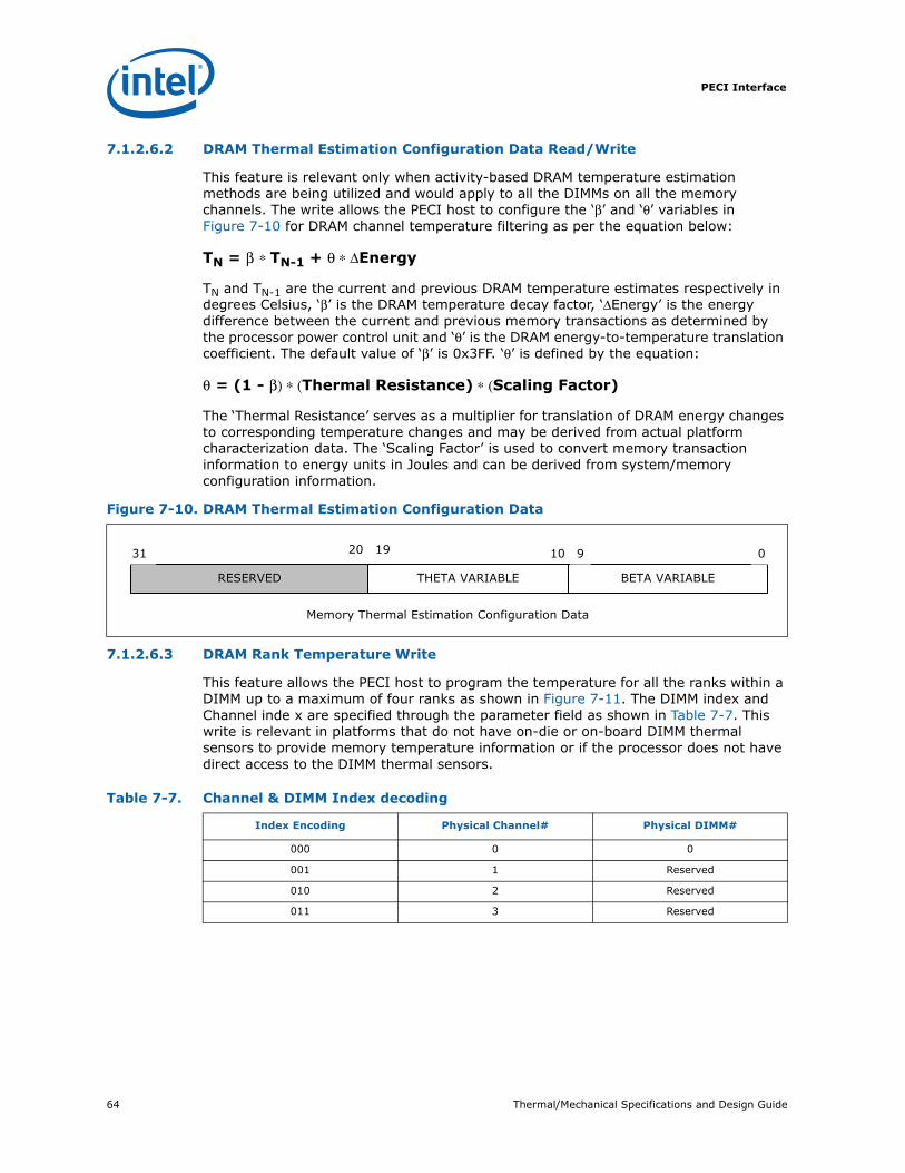
PECI Interface
64 Thermal/Mechanical Specifications and Design Guide
7.1.2.6.2 DRAM Thermal Estimation Configuration Data Read/Write
This feature is relevant only when activity-based DRAM temperature estimation methods are being utilized and would apply to all the DIMMs on all the memory channels. The write allows the PECI host to configure the ‘β’ and ‘θ’ variables in Figure 7-10 for DRAM channel temperature filtering as per the equation below:
TN = β ∗ TN-1 + θ ∗ ΔEnergy
TN and TN-1 are the current and previous DRAM temperature estimates respectively in degrees Celsius, ‘β’ is the DRAM temperature decay factor, ‘ΔEnergy’ is the energy difference between the current and previous memory transactions as determined by the processor power control unit and ‘θ’ is the DRAM energy-to-temperature translation coefficient. The default value of ‘β’ is 0x3FF. ‘θ’ is defined by the equation:
θ = (1 - β) ∗ (Thermal Resistance) ∗ (Scaling Factor)
The ‘Thermal Resistance’ serves as a multiplier for translation of DRAM energy changes to corresponding temperature changes and may be derived from actual platform characterization data. The ‘Scaling Factor’ is used to convert memory transaction information to energy units in Joules and can be derived from system/memory configuration information.
7.1.2.6.3 DRAM Rank Temperature Write
This feature allows the PECI host to program the temperature for all the ranks within a DIMM up to a maximum of four ranks as shown in Figure 7-11. The DIMM index and Channel inde x are specified through the parameter field as shown in Table 7-7. This write is relevant in platforms that do not have on-die or on-board DIMM thermal sensors to provide memory temperature information or if the processor does not have direct access to the DIMM thermal sensors.
Figure 7-10. DRAM Thermal Estimation Configuration Data
Memory Thermal Estimation Configuration Data
RESERVED
1031
BETA VARIABLE
9 0
THETA VARIABLE
1920
Table 7-7. Channel & DIMM Index decoding
Index Encoding Physical Channel# Physical DIMM#
000 0 0
001 1 Reserved
010 2 Reserved
011 3 Reserved
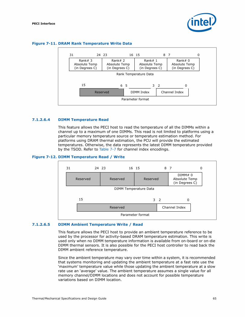
Thermal/Mechanical Specifications and Design Guide 65
PECI Interface
7.1.2.6.4 DIMM Temperature Read
This feature allows the PECI host to read the temperature of all the DIMMs within a channel up to a maximum of one DIMMs. This read is not limited to platforms using a particular memory temperature source or temperature estimation method. For platforms using DRAM thermal estimation, the PCU will provide the estimated temperatures. Otherwise, the data represents the latest DIMM temperature provided by the TSOD. Refer to Table 7-7 for channel index encodings.
7.1.2.6.5 DIMM Ambient Temperature Write / Read
This feature allows the PECI host to provide an ambient temperature reference to be used by the processor for activity-based DRAM temperature estimation. This write is used only when no DIMM temperature information is available from on-board or on-die DIMM thermal sensors. It is also possible for the PECI host controller to read back the DIMM ambient reference temperature.
Since the ambient temperature may vary over time within a system, it is recommended that systems monitoring and updating the ambient temperature at a fast rate use the ‘maximum’ temperature value while those updating the ambient temperature at a slow rate use an ‘average’ value. The ambient temperature assumes a single value for all memory channel/DIMM locations and does not account for possible temperature variations based on DIMM location.
Figure 7-11. DRAM Rank Temperature Write Data
15 7 0
Rank Temperature Data
Rank# 3 Absolute Temp(in Degrees C)
Rank# 2 Absolute Temp(in Degrees C)
Rank# 1 Absolute Temp(in Degrees C)
Rank# 0 Absolute Temp(in Degrees C)
816232431
15 2
Parameter format
Reserved DIMM Index
6
Channel Index
5 3 0
Figure 7-12. DIMM Temperature Read / Write
15 7 0
DIMM Temperature Data
Reserved ReservedDIMM# 0
Absolute Temp(in Degrees C)
816232431
15 2
Parameter format
Reserved Channel Index
3 0
Reserved

PECI Interface
66 Thermal/Mechanical Specifications and Design Guide
7.1.2.6.6 DRAM Channel Temperature Read
This feature enables a PECI host read of the maximum temperature of each channel. This would include all the DIMMs within the channel and all the ranks with each of the DIMMs. Channels that are not populated will return the ‘ambient temperature’ on systems using activity-based temperature estimations or alternatively return a ‘zero’ for systems using sensor-based temperatures.
7.1.2.6.7 Accumulated DRAM Energy Read
This feature allows the PECI host to read the DRAM energy consumed by all the DIMMs within all the channels or all the DIMMs within just a specified channel. The parameter field is used to specify the channel index. Units used are defined as per the Package Power SKU Unit read described in Section 7.1.2.7. This information is tracked by a 32-bit counter that wraps around. Note that the channel index in Figure 7-15 is specified as per the index encoding described in Table 7-7. A channel index of 0x00FF is used to specify the “all channels” case.
Figure 7-13. Ambient Temperature Reference Data
7 0
Ambient Temperature Reference Data
ReservedAmbient
Temperature (in Degrees C)
831
Figure 7-14. DRAM Channel Temperature
15 7 0
Channel Temperature Data
Channel 3 Maximum
Temperature(in Degrees C)
Channel 2 Maximum
Temperature(in Degrees C)
Channel 1 Maximum
Temperature(in Degrees C)
Channel 0 Maximum
Temperature(in Degrees C)
816232431
Figure 7-15. Accumulated DRAM Energy Data
0
Accumulated DRAM Energy Data
Accumulated DRAM Energy
31
15 2
Parameter format
Reserved Channel Index
3 0
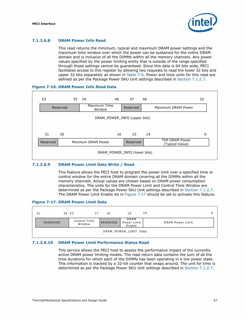
Thermal/Mechanical Specifications and Design Guide 67
PECI Interface
7.1.2.6.8 DRAM Power Info Read
This read returns the minimum, typical and maximum DRAM power settings and the maximum time window over which the power can be sustained for the entire DRAM domain and is inclusive of all the DIMMs within all the memory channels. Any power values specified by the power limiting entity that is outside of the range specified through these settings cannot be guaranteed. Since this data is 64 bits wide, PECI facilitates access to this register by allowing two requests to read the lower 32 bits and upper 32 bits separately as shown in Table 7-6. Power and time units for this read are defined as per the Package Power SKU Unit settings described in Section 7.1.2.7.
7.1.2.6.9 DRAM Power Limit Data Write / Read
This feature allows the PECI host to program the power limit over a specified time or control window for the entire DRAM domain covering all the DIMMs within all the memory channels. Actual values are chosen based on DRAM power consumption characteristics. The units for the DRAM Power Limit and Control Time Window are determined as per the Package Power SKU Unit settings described in Section 7.1.2.7. The DRAM Power Limit Enable bit in Figure 7-17 should be set to activate this feature.
7.1.2.6.10 DRAM Power Limit Performance Status Read
This service allows the PECI host to assess the performance impact of the currently active DRAM power limiting modes. The read return data contains the sum of all the time durations for which each of the DIMMs has been operating in a low power state. This information is tracked by a 32-bit counter that wraps around. The unit for time is determined as per the Package Power SKU Unit settings described in Section 7.1.2.7.
Figure 7-16. DRAM Power Info Read Data
DRAM_POWER_INFO (lower bits)
Reserved
14
Minimum DRAM Power
16
TDP DRAM Power (Typical Value)
30 015
Reserved
31
DRAM_POWER_INFO (upper bits)
Maximum DRAM Power
3246
Reserved
47
Maximum Time Window
4854
Reserved
5563
Figure 7-17. DRAM Power Limit Data
DRAM_POWER_LIMIT Data
DRAM Power Lim it
Enable
1523
DRAM Power Lim it
14 0
RESERVED
16
Control Time Window
1731
RESERVED
24

PECI Interface
68 Thermal/Mechanical Specifications and Design Guide
7.1.2.7 Processor Thermal and Power Optimization Capabilities
Figure 7-18. DRAM Power Limit Performance Data
Table 7-8. RdPkgConfig() & WrPkgConfig() Processor Thermal and Power OptimizationServices Summary (Sheet 1 of 3)
ServiceIndex Value(byte)
Parameter Value
(word)
RdPkgConfig()Data
(dword)
WrPkgConfig()Data
(dword)Description
Package Identifier Read 00
0x0000 CPUID Information
Returns processor-specific information including processor family, model and stepping information.
0x0001 Platform ID Returns platform segment information.
0x0002 Uncore Device ID Returns Uncore Device ID information.
0x0003 Max Thread ID Returns the maximum ‘Thread ID’ value supported by the processor.
0x0004 CPU Microcode Update Revision
Returns microcode update and firmware revision information.
0x0005 Machine Check Status
Returns machine check status
Package Power SKU Unit Read 30 0x0000 Time, Energy and
Power Units N/ARead units for power, energy and time used in power control registers.
Package Power SKU [LOW] Read 28 0x0000 Package Power
SKU[31:0] N/AReturns Thermal Design Power and minimum package power values for the processor SKU.
Package Power SKU [HIGH]
Read29 0x0000 Package Power
SKU[64:32] N/A
Returns the maximum package power value for the processor SKU and the maximum time interval for which it can be sustained.
“Wake on PECI” mode bit Write 05 0x0001 - Set
0x0000 - Reset N/A “Wake on PECI” mode bit
Enables package pop-up to C2 to service PECI PCIConfig() accesses if appropriate.
“Wake on PECI” mode bit Read 05 0x0000 “Wake on PECI” mode
bit N/A Read status of “Wake on PECI” mode bit
Accumulated Run Time Read 31 0x0000 Total reference time N/A Returns the total run time.
Package Temperature
Read02 0x00FF Processor package
Temperature N/AReturns the maximum processor die temperature in PECI format.
Temperature Target Read 16 0x0000 Processor Tjmax and
TCONTROLN/A
Returns the maximum processor junction temperature and processor TCONTROL.
DRAM Power Limit Performance
Accumulated DRAM Throttle Time
031
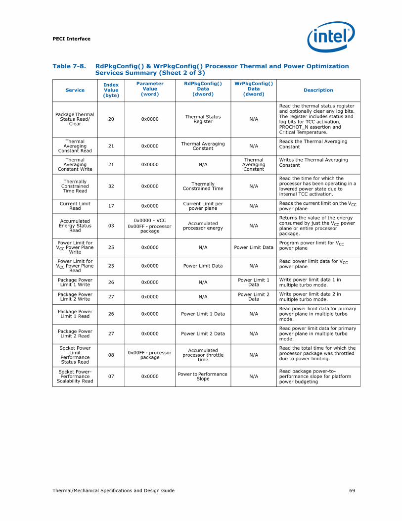
Thermal/Mechanical Specifications and Design Guide 69
PECI Interface
Package Thermal Status Read/
Clear20 0x0000 Thermal Status
Register N/A
Read the thermal status register and optionally clear any log bits. The register includes status and log bits for TCC activation, PROCHOT_N assertion and Critical Temperature.
Thermal Averaging
Constant Read21 0x0000 Thermal Averaging
Constant N/AReads the Thermal Averaging Constant
Thermal Averaging
Constant Write21 0x0000 N/A
Thermal Averaging Constant
Writes the Thermal Averaging Constant
Thermally Constrained Time Read
32 0x0000 Thermally Constrained Time N/A
Read the time for which the processor has been operating in a lowered power state due to internal TCC activation.
Current Limit Read 17 0x0000 Current Limit per
power plane N/A Reads the current limit on the VCC power plane
Accumulated Energy Status
Read03
0x0000 - VCC0x00FF - processor
packageAccumulated
processor energy N/A
Returns the value of the energy consumed by just the VCC power plane or entire processor package.
Power Limit for VCC Power Plane
Write25 0x0000 N/A Power Limit Data
Program power limit for VCC power plane
Power Limit for VCC Power Plane
Read25 0x0000 Power Limit Data N/A
Read power limit data for VCC power plane
Package Power Limit 1 Write 26 0x0000 N/A Power Limit 1
DataWrite power limit data 1 in multiple turbo mode.
Package Power Limit 2 Write 27 0x0000 N/A Power Limit 2
DataWrite power limit data 2 in multiple turbo mode.
Package Power Limit 1 Read 26 0x0000 Power Limit 1 Data N/A
Read power limit data for primary power plane in multiple turbo mode.
Package Power Limit 2 Read 27 0x0000 Power Limit 2 Data N/A
Read power limit data for primary power plane in multiple turbo mode.
Socket Power Limit
Performance Status Read
08 0x00FF - processor package
Accumulated processor throttle
timeN/A
Read the total time for which the processor package was throttled due to power limiting.
Socket Power-Performance
Scalability Read07 0x0000 Power to Performance
Slope N/ARead package power-to-performance slope for platform power budgeting
Table 7-8. RdPkgConfig() & WrPkgConfig() Processor Thermal and Power OptimizationServices Summary (Sheet 2 of 3)
ServiceIndex Value(byte)
Parameter Value
(word)
RdPkgConfig()Data
(dword)
WrPkgConfig()Data
(dword)Description
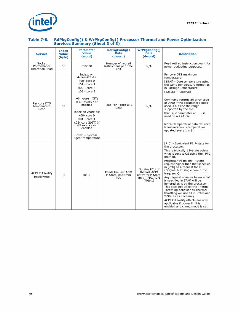
PECI Interface
70 Thermal/Mechanical Specifications and Design Guide
Socket Performance
Indication Read06 0x0000
Number of retired instructions per time
unitN/A
Read retired instruction count for power budgeting purposes.
Per core DTS temperature
Read09
Index: on 4core+GT diex00- core 0x01 - core 1x02 - core 2x03 - core 3
x04 -core 4(GT) If GT exists / or
enabled
Index on 2core diex00- core 0x01 - core 1
x02- core 2(GT) If GT exists / or
enabled
0xFF – System Agent temperature
Read Per - core DTS data N/A
Per core DTS maximum temperature[15:0] - Core temperature using the same temperature format as in Package Temperature.[32:16] – Reserved
Command returns an error code of 0x90 if the parameter (index) used is outside the range supported by the die. that is, if parameter of 3..5 is used on a 2+1 die
Note: Temperature data returned is instantaneous temperature updated every 1 mS.
ACPI P-T NotifyRead/Write 33 0x00
Reads the last ACPI P-State limit from
PCU
Notifies PCU of the last ACPI
notify for P-State limit (_PPC ACPI
Object)
[7:0] - Equivalent P1 P-state for the processor. This is typically 1 P-state below what is sent to OS using the _PPC method.Processor treats any P-State request higher than that specified in [7:0] as a request for P0 (Original Max single core turbo frequency).Any request equal or below what is specified in [7:0] will be honored as is by the processor. This does not affect the Thermal Throttling behavior as Thermal throttling will use all P-States and T-States as necessary.ACPI P-T Notify effects are only applicable if power limit is enabled and clamp mode is set
Table 7-8. RdPkgConfig() & WrPkgConfig() Processor Thermal and Power OptimizationServices Summary (Sheet 3 of 3)
ServiceIndex Value(byte)
Parameter Value
(word)
RdPkgConfig()Data
(dword)
WrPkgConfig()Data
(dword)Description

Thermal/Mechanical Specifications and Design Guide 71
PECI Interface
7.1.2.7.1 Package Identifier Read
This feature enables the PECI host to uniquely identify the PECI client processor. The parameter field encodings shown in Table 7-8 allow the PECI host to access the relevant processor information as described below.
• CPUID data: This is the equivalent of data that can be accessed through the CPUID instruction execution. It contains processor type, stepping, model and family ID information as shown in Figure 7-19.
• Platform ID data: The Platform ID data identifies the platform type that the processor is being used on as per the encodings in Table 7-9. The Platform ID data can be used to ensure processor microcode updates are compatible with the processor. Note that the value of the Platform ID or Processor Flag[2:0] as shown in Figure 7-20 is typically unique to the platform type and processor stepping.
• Uncore Device ID: This information can be used to uniquely identify the processor device when combined with the Vendor Identification register content. Refer to the appropriate register description for the exact Intel® Core™ i7-3960X, i7-3970X processor Extreme Edition, Intel® Core™ i7-3930K processor, and Intel® Core™ i7-3820 processor Uncore Device ID value.
Figure 7-19. CPUID Data
CPU ID Data
Model
420
Stepping ID
3 0
Family ID
16
Processor Type
1931
RESERVED
27
Extended Model
Extended Family ID
78111228
RESERVED
1315
Table 7-9. Platform ID Encoding
Platform ID Platform Type
0x00000000 DP (Dual Processor)
0x00000001 UP (Single Processor)
0x00000002 Reserved
All Others Reserved
Figure 7-20. Platform ID Data
Platform ID Data
Processor FlagReserved
231 03
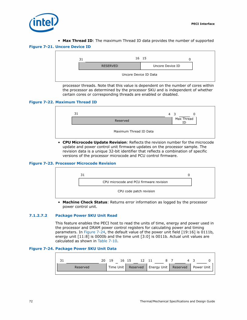
PECI Interface
72 Thermal/Mechanical Specifications and Design Guide
• Max Thread ID: The maximum Thread ID data provides the number of supported
processor threads. Note that this value is dependent on the number of cores within the processor as determined by the processor SKU and is independent of whether certain cores or corresponding threads are enabled or disabled.
• CPU Microcode Update Revision: Reflects the revision number for the microcode update and power control unit firmware updates on the processor sample. The revision data is a unique 32-bit identifier that reflects a combination of specific versions of the processor microcode and PCU control firmware.
• Machine Check Status: Returns error information as logged by the processor power control unit.
7.1.2.7.2 Package Power SKU Unit Read
This feature enables the PECI host to read the units of time, energy and power used in the processor and DRAM power control registers for calculating power and timing parameters. In Figure 7-24, the default value of the power unit field [19:16] is 0111b, energy unit [11:8] is 0000b and the time unit [3:0] is 0011b. Actual unit values are calculated as shown in Table 7-10.
Figure 7-21. Uncore Device ID
Uncore Device ID Data
RESERVED
031
Uncore Device ID
1516
Figure 7-22. Maximum Thread ID
Maximum Thread ID Data
Max Thread IDReserved
331 04
Figure 7-23. Processor Microcode Revision
CPU microcode and PCU firmware revision
31 0
CPU code patch revision
Figure 7-24. Package Power SKU Unit Data
Reserved
2031
Time Unit
19
Reserved
16 15
Energy Unit
11 8
Reserved Power Unit
12 7 4 3 0
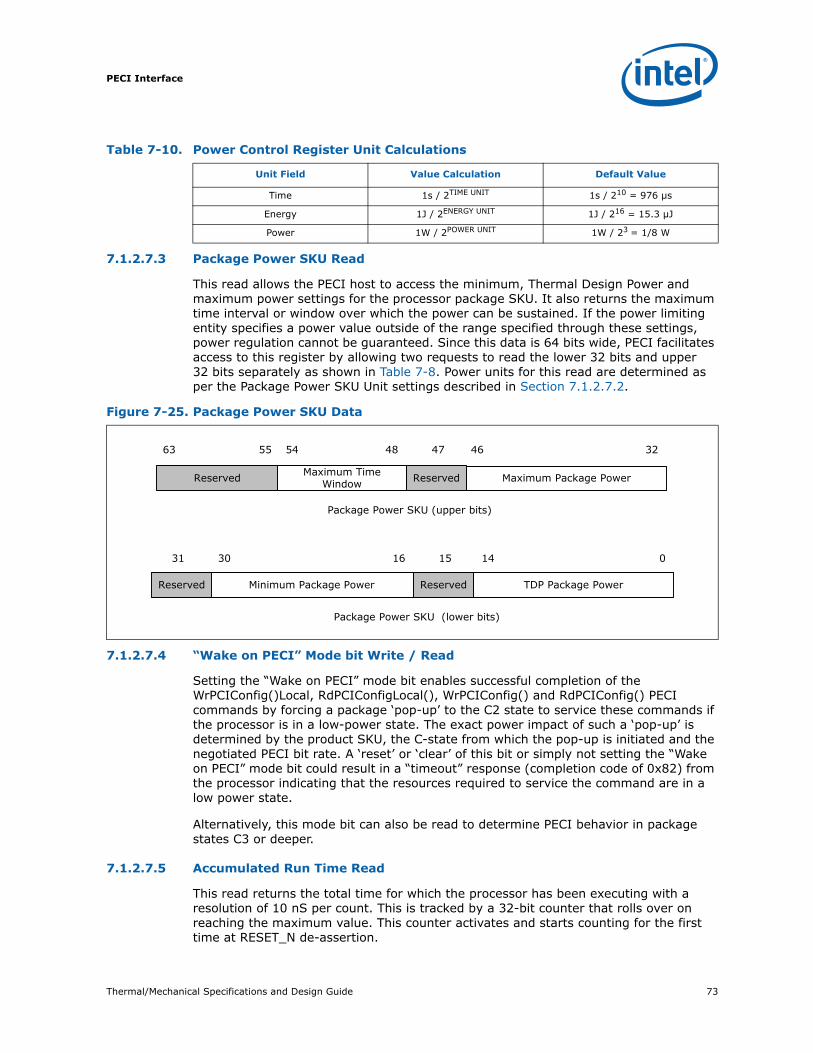
Thermal/Mechanical Specifications and Design Guide 73
PECI Interface
7.1.2.7.3 Package Power SKU Read
This read allows the PECI host to access the minimum, Thermal Design Power and maximum power settings for the processor package SKU. It also returns the maximum time interval or window over which the power can be sustained. If the power limiting entity specifies a power value outside of the range specified through these settings, power regulation cannot be guaranteed. Since this data is 64 bits wide, PECI facilitates access to this register by allowing two requests to read the lower 32 bits and upper 32 bits separately as shown in Table 7-8. Power units for this read are determined as per the Package Power SKU Unit settings described in Section 7.1.2.7.2.
7.1.2.7.4 “Wake on PECI” Mode bit Write / Read
Setting the “Wake on PECI” mode bit enables successful completion of the WrPCIConfig()Local, RdPCIConfigLocal(), WrPCIConfig() and RdPCIConfig() PECI commands by forcing a package ‘pop-up’ to the C2 state to service these commands if the processor is in a low-power state. The exact power impact of such a ‘pop-up’ is determined by the product SKU, the C-state from which the pop-up is initiated and the negotiated PECI bit rate. A ‘reset’ or ‘clear’ of this bit or simply not setting the “Wake on PECI” mode bit could result in a “timeout” response (completion code of 0x82) from the processor indicating that the resources required to service the command are in a low power state.
Alternatively, this mode bit can also be read to determine PECI behavior in package states C3 or deeper.
7.1.2.7.5 Accumulated Run Time Read
This read returns the total time for which the processor has been executing with a resolution of 10 nS per count. This is tracked by a 32-bit counter that rolls over on reaching the maximum value. This counter activates and starts counting for the first time at RESET_N de-assertion.
Table 7-10. Power Control Register Unit Calculations
Unit Field Value Calculation Default Value
Time 1s / 2TIME UNIT 1s / 210 = 976 µs
Energy 1J / 2ENERGY UNIT 1J / 216 = 15.3 µJ
Power 1W / 2POWER UNIT 1W / 23 = 1/8 W
Figure 7-25. Package Power SKU Data
Package Power SKU (lower bits)
Reserved
14
Minimum Package Power
16
TDP Package Power
30 015
Reserved
31
Package Power SKU (upper bits)
Maximum Package Power
3246
Reserved
47
Maximum Time Window
4854
Reserved
5563
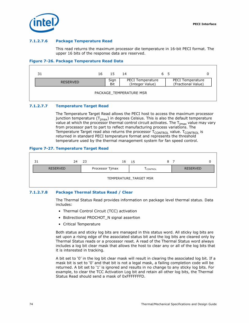
PECI Interface
74 Thermal/Mechanical Specifications and Design Guide
7.1.2.7.6 Package Temperature Read
This read returns the maximum processor die temperature in 16-bit PECI format. The upper 16 bits of the response data are reserved.
7.1.2.7.7 Temperature Target Read
The Temperature Target Read allows the PECI host to access the maximum processor junction temperature (Tjmax) in degrees Celsius. This is also the default temperature value at which the processor thermal control circuit activates. The Tjmax value may vary from processor part to part to reflect manufacturing process variations. The Temperature Target read also returns the processor TCONTROL value. TCONTROL is returned in standard PECI temperature format and represents the threshold temperature used by the thermal management system for fan speed control.
7.1.2.7.8 Package Thermal Status Read / Clear
The Thermal Status Read provides information on package level thermal status. Data includes:
• Thermal Control Circuit (TCC) activation
• Bidirectional PROCHOT_N signal assertion
• Critical Temperature
Both status and sticky log bits are managed in this status word. All sticky log bits are set upon a rising edge of the associated status bit and the log bits are cleared only by Thermal Status reads or a processor reset. A read of the Thermal Status word always includes a log bit clear mask that allows the host to clear any or all of the log bits that it is interested in tracking.
A bit set to ‘0’ in the log bit clear mask will result in clearing the associated log bit. If a mask bit is set to ‘0’ and that bit is not a legal mask, a failing completion code will be returned. A bit set to ‘1’ is ignored and results in no change to any sticky log bits. For example, to clear the TCC Activation Log bit and retain all other log bits, the Thermal Status Read should send a mask of 0xFFFFFFFD.
Figure 7-26. Package Temperature Read Data
PACKAGE_TEMPERATURE MSR
Sign Bit
14
RESERVED
16
PECI Temperature (Integer Value)
61531
PECI Temperature(Fractional Value)
5 0
Figure 7-27. Temperature Target Read
TEMPERATURE_TARGET MSR
15
Processor Tjmax
16
TCONTROL
823
RESERVED
7 0
RESERVED
31 24
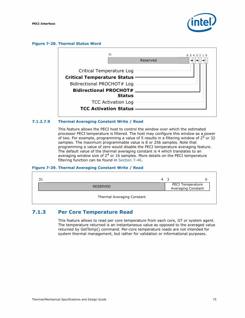
Thermal/Mechanical Specifications and Design Guide 75
PECI Interface
7.1.2.7.9 Thermal Averaging Constant Write / Read
This feature allows the PECI host to control the window over which the estimated processor PECI temperature is filtered. The host may configure this window as a power of two. For example, programming a value of 5 results in a filtering window of 25 or 32 samples. The maximum programmable value is 8 or 256 samples. Note that programming a value of zero would disable the PECI temperature averaging feature. The default value of the thermal averaging constant is 4 which translates to an averaging window size of 24 or 16 samples. More details on the PECI temperature filtering function can be found in Section 7-46.
7.1.3 Per Core Temperature ReadThis feature allows to read per core temperature from each core, GT or system agent. The temperature returned is an instantaneous value as opposed to the averaged value returned by GetTemp() command. Per-core temperature reads are not intended for system thermal management, but rather for validation or informational purposes.
Figure 7-28. Thermal Status Word
Critical Temperature Log Critical Temperature Status
Bidirectional PROCHOT# LogBidirectional PROCHOT#
StatusTCC Activation Log
TCC Activation Status
31 6 5 4 3 2 1 0
Reserved
Figure 7-29. Thermal Averaging Constant Write / Read
Thermal Averaging Constant
RESERVED
431PECI Temperature
Averaging Constant
3 0

PECI Interface
76 Thermal/Mechanical Specifications and Design Guide
7.1.4 ACPI P-T Notify Read/WriteThis interface coupled with limiting OSPM usage of P-States using ACPI _PPC object and programming of the package power limit registers enables turbo capability while limiting maximum package power dissipation to be within the specified package power limit.
7.1.4.1 Thermally Constrained Time Read
This features allows the PECI host to access the total time for which the processor has been operating in a lowered power state due to TCC activation. The returned data includes the time required to ramp back up to the original P-state target after TCC activation expires. This timer does not include TCC activation as a result of an external assertion of PROCHOT_N. This is tracked by a 32-bit counter that rolls over or wraps around. Note that on the processor PECI clients, the only logic that can be thermally constrained is that supplied by VCC.
7.1.4.2 Current Limit Read
This read returns the current limit for the processor VCC power plane in 1/8A increments. Actual current limit data is contained only in the lower 13 bits of the response data. The default return value of 0x258 corresponds to a current limit value of 75 A.
7.1.4.3 Accumulated Energy Status Read
This service can return the value of the total energy consumed by the entire processor package or just the logic supplied by the VCC power plane as specified through the parameter field in Table 7-8. This information is tracked by a 32-bit counter that wraps around and continues counting on reaching its limit. Energy units for this read are determined as per the Package Power SKU Unit settings described in Section 7.1.2.7.2.
Figure 7-30. Current Config Limit Read Data
Current Config Limit Data
RESERVED
1331
Current Limit for processor VCC
12 0
Figure 7-31. Accumulated Energy Read Data
Accumulated Energy Status
Accumulated CPU Energy
031

Thermal/Mechanical Specifications and Design Guide 77
PECI Interface
7.1.4.4 Power Limit for the VCC Power Plane Write / Read
This feature allows the PECI host to program the power limit over a specified time or control window for the VCC power plane. Actual values are chosen based on the VR (voltage regulator) capabilities. The units for the Power Limit and Control Time Window are determined as per the Package Power SKU Unit settings described in Section 7.1.2.7.2. The Power Limit Enable bit in Figure 7-32 should be set to activate this feature. Setting the Clamp Mode bit allows the cores to go into power states below what the operating system originally requested.
7.1.4.5 Package Power Limits For Multiple Turbo Modes
This feature allows the PECI host to program two power limit values to support multiple turbo modes. The operating systems and drivers can balance the power budget using these two limits. Two separate PECI requests are available to program the lower and upper 32 bits of the power limit data shown in Figure 7-33. The units for the Power Limit and Control Time Window are determined as per the Package Power SKU Unit settings described in Section 7.1.2.7.2. Setting the Clamp Mode bit allows the cores to go into power states below what the operating system originally requested. The Power Limit Enable bit should be set to enable the power limiting function.
Figure 7-32. Power Limit Data for VCC Power Plane
VCC Power Plane Power Limit Data
Power Limit Enable
1523
VCC Plane Power Limit
14 0
Clamp Mode
16
Control Time Window
1731
RESERVED
24
Figure 7-33. PKG_TURBO_POWER_LIMIT Data
Package Power Limit 1
Power Limit Enable #1
1523
Power Limit # 1
14 0
Clamp Mode #1
16
Control Time Window #1
1731
RESERVED
24
Package Power Limit 2
Power Limit Enable #2
4755
Power Limit # 2
46 32
Clamp Mode #2
48
Control Time Window #2
4963
RESERVED
56
PECI Interface
78 Thermal/Mechanical Specifications and Design Guide
7.1.4.6 Socket Power Limit Performance Status Read
This service allows the PECI host to assess the performance impact of the currently active power limiting modes. The read return data contains the total amount of time for which the entire processor package has been operating in a power state that is lower than what the operating system originally requested. This information is tracked by a 32-bit counter that wraps around. The unit for time is determined as per the Package Power SKU Unit settings described in Section 7.1.2.7.2.
7.1.4.7 Socket Power-Performance Scalability Read
This feature allows the PECI host to access time-averaged processor package power-performance ratio information at the current workload and operating point. This is typically used to maximize overall platform performance-power ratios by appropriate budgeting between multiple packages.
7.1.4.8 Socket Performance Indication Read
This read returns information on the total number of retired instructions and is monitored by a 32-bit counter. It may be used in conjunction with the ‘Accumulated Run Time Read’ described in Section 7.1.2.7.5 to track the number of retired instructions per time unit. This feature is typically used for power budgeting through appropriate distribution of power across racks of heterogeneous platforms. Note the following equation for calculation for the actual number of retried instructions.
Number of retried instructions = Socket Performance Indication Data * 128
Figure 7-34. Socket Power Limit Performance Data
Accumulated CPU Throttle Time
Accumulated CPU Throttle Time
031
Figure 7-35. Socket Power-Performance Scalability Data
Processor Power-Performance Ratio Data
CPU Socket Power-Performance Ratio
031
Figure 7-36. Socket Performance Indication Data
Socket Performance Indication
Socket Performance Indication Data
031
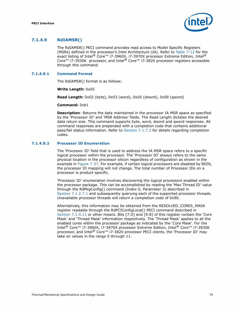
Thermal/Mechanical Specifications and Design Guide 79
PECI Interface
7.1.4.9 RdIAMSR()
The RdIAMSR() PECI command provides read access to Model Specific Registers (MSRs) defined in the processor’s Intel Architecture (IA). Refer to Table 7-12 for the exact listing of Intel® Core™ i7-3960X, i7-3970X processor Extreme Edition, Intel® Core™ i7-3930K processor, and Intel® Core™ i7-3820 processor registers accessible through this command.
7.1.4.9.1 Command Format
The RdIAMSR() format is as follows:
Write Length: 0x05
Read Length: 0x02 (byte), 0x03 (word), 0x05 (dword), 0x09 (qword)
Command: 0xb1
Description: Returns the data maintained in the processor IA MSR space as specified by the ‘Processor ID’ and ‘MSR Address’ fields. The Read Length dictates the desired data return size. This command supports byte, word, dword and qword responses. All command responses are prepended with a completion code that contains additional pass/fail status information. Refer to Section 7.1.7.2 for details regarding completion codes.
7.1.4.9.2 Processor ID Enumeration
The ‘Processor ID’ field that is used to address the IA MSR space refers to a specific logical processor within the processor. The ‘Processor ID’ always refers to the same physical location in the processor silicon regardless of configuration as shown in the example in Figure 7-37. For example, if certain logical processors are disabled by BIOS, the processor ID mapping will not change. The total number of Processor IDs on a processor is product-specific.
‘Processor ID’ enumeration involves discovering the logical processors enabled within the processor package. This can be accomplished by reading the ‘Max Thread ID’ value through the RdPkgConfig() command (Index 0, Parameter 3) described in Section 7.1.2.7.1 and subsequently querying each of the supported processor threads. Unavailable processor threads will return a completion code of 0x90.
Alternatively, this information may be obtained from the RESOLVED_CORES_MASK register readable through the RdPCIConfigLocal() PECI command described in Section 7.1.4.11 or other means. Bits [7:0] and [9:8] of this register contain the ‘Core Mask’ and ‘Thread Mask’ information respectively. The ‘Thread Mask’ applies to all the enabled cores within the processor package as indicated by the ‘Core Mask’. For the Intel® Core™ i7-3960X, i7-3970X processor Extreme Edition, Intel® Core™ i7-3930K processor, and Intel® Core™ i7-3820 processor PECI clients, the ‘Processor ID’ may take on values in the range 0 through 11.
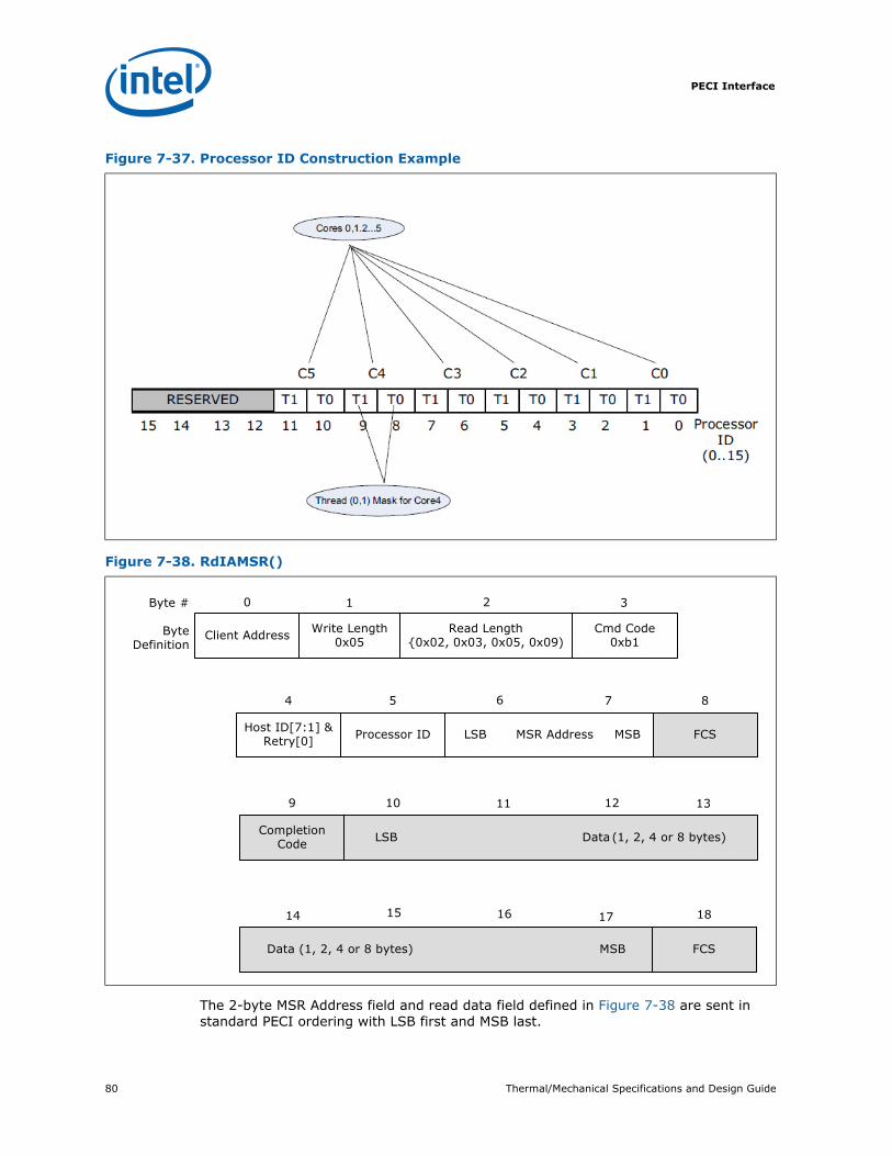
PECI Interface
80 Thermal/Mechanical Specifications and Design Guide
The 2-byte MSR Address field and read data field defined in Figure 7-38 are sent in standard PECI ordering with LSB first and MSB last.
Figure 7-37. Processor ID Construction Example
Figure 7-38. RdIAMSR()
<Process Name>
1 3
Byte Definition
Byte # 0 2
15 17
Data (1, 2, 4 or 8 bytes) MSB
14 16 18
FCS
Read Length {0x02, 0x03, 0x05, 0x09)
Cmd Code0xb1
LSB Data (1, 2, 4 or 8 bytes)
Write Length0x05
9 11
86
CompletionCode
Processor ID
5
13
4
LSB MSR Address MSB
Client Address
10
7
FCSHost ID[7:1] & Retry[0]
12
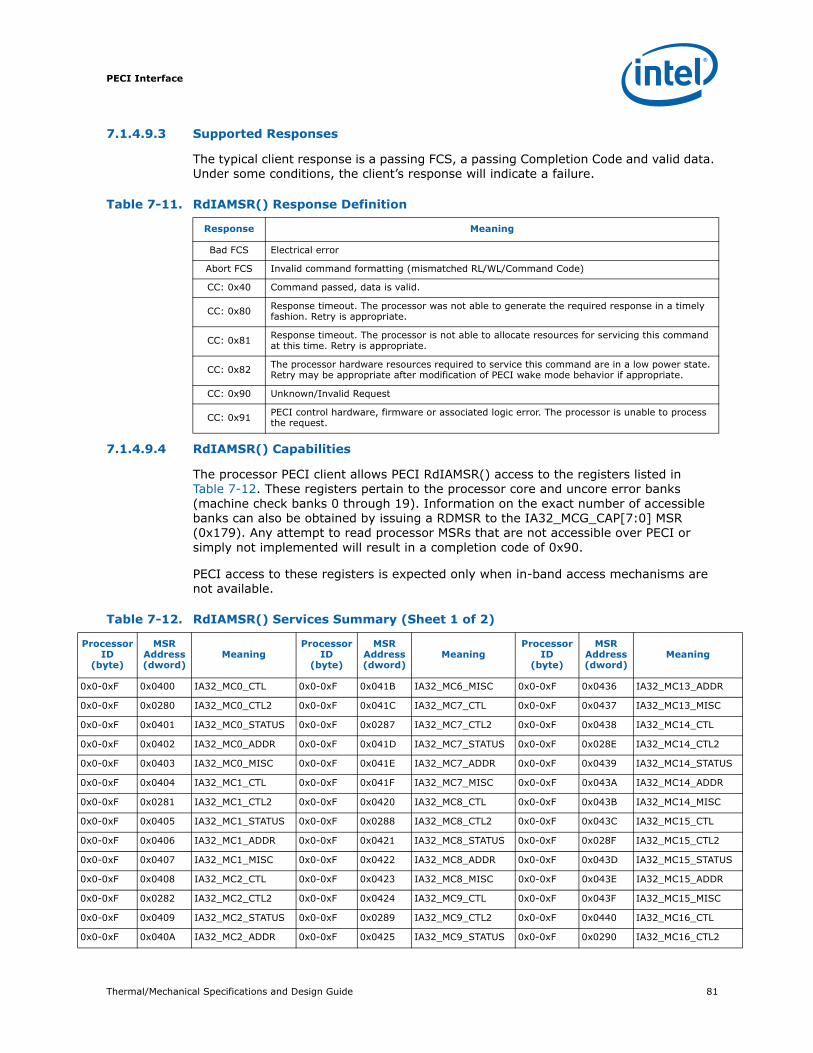
Thermal/Mechanical Specifications and Design Guide 81
PECI Interface
7.1.4.9.3 Supported Responses
The typical client response is a passing FCS, a passing Completion Code and valid data. Under some conditions, the client’s response will indicate a failure.
7.1.4.9.4 RdIAMSR() Capabilities
The processor PECI client allows PECI RdIAMSR() access to the registers listed in Table 7-12. These registers pertain to the processor core and uncore error banks (machine check banks 0 through 19). Information on the exact number of accessible banks can also be obtained by issuing a RDMSR to the IA32_MCG_CAP[7:0] MSR (0x179). Any attempt to read processor MSRs that are not accessible over PECI or simply not implemented will result in a completion code of 0x90.
PECI access to these registers is expected only when in-band access mechanisms are not available.
Table 7-11. RdIAMSR() Response Definition
Response Meaning
Bad FCS Electrical error
Abort FCS Invalid command formatting (mismatched RL/WL/Command Code)
CC: 0x40 Command passed, data is valid.
CC: 0x80 Response timeout. The processor was not able to generate the required response in a timely fashion. Retry is appropriate.
CC: 0x81 Response timeout. The processor is not able to allocate resources for servicing this command at this time. Retry is appropriate.
CC: 0x82 The processor hardware resources required to service this command are in a low power state. Retry may be appropriate after modification of PECI wake mode behavior if appropriate.
CC: 0x90 Unknown/Invalid Request
CC: 0x91 PECI control hardware, firmware or associated logic error. The processor is unable to process the request.
Table 7-12. RdIAMSR() Services Summary (Sheet 1 of 2)
Processor ID
(byte)
MSR Address (dword)
MeaningProcessor
ID(byte)
MSR Address (dword)
MeaningProcessor
ID(byte)
MSR Address (dword)
Meaning
0x0-0xF 0x0400 IA32_MC0_CTL 0x0-0xF 0x041B IA32_MC6_MISC 0x0-0xF 0x0436 IA32_MC13_ADDR
0x0-0xF 0x0280 IA32_MC0_CTL2 0x0-0xF 0x041C IA32_MC7_CTL 0x0-0xF 0x0437 IA32_MC13_MISC
0x0-0xF 0x0401 IA32_MC0_STATUS 0x0-0xF 0x0287 IA32_MC7_CTL2 0x0-0xF 0x0438 IA32_MC14_CTL
0x0-0xF 0x0402 IA32_MC0_ADDR 0x0-0xF 0x041D IA32_MC7_STATUS 0x0-0xF 0x028E IA32_MC14_CTL2
0x0-0xF 0x0403 IA32_MC0_MISC 0x0-0xF 0x041E IA32_MC7_ADDR 0x0-0xF 0x0439 IA32_MC14_STATUS
0x0-0xF 0x0404 IA32_MC1_CTL 0x0-0xF 0x041F IA32_MC7_MISC 0x0-0xF 0x043A IA32_MC14_ADDR
0x0-0xF 0x0281 IA32_MC1_CTL2 0x0-0xF 0x0420 IA32_MC8_CTL 0x0-0xF 0x043B IA32_MC14_MISC
0x0-0xF 0x0405 IA32_MC1_STATUS 0x0-0xF 0x0288 IA32_MC8_CTL2 0x0-0xF 0x043C IA32_MC15_CTL
0x0-0xF 0x0406 IA32_MC1_ADDR 0x0-0xF 0x0421 IA32_MC8_STATUS 0x0-0xF 0x028F IA32_MC15_CTL2
0x0-0xF 0x0407 IA32_MC1_MISC 0x0-0xF 0x0422 IA32_MC8_ADDR 0x0-0xF 0x043D IA32_MC15_STATUS
0x0-0xF 0x0408 IA32_MC2_CTL 0x0-0xF 0x0423 IA32_MC8_MISC 0x0-0xF 0x043E IA32_MC15_ADDR
0x0-0xF 0x0282 IA32_MC2_CTL2 0x0-0xF 0x0424 IA32_MC9_CTL 0x0-0xF 0x043F IA32_MC15_MISC
0x0-0xF 0x0409 IA32_MC2_STATUS 0x0-0xF 0x0289 IA32_MC9_CTL2 0x0-0xF 0x0440 IA32_MC16_CTL
0x0-0xF 0x040A IA32_MC2_ADDR 0x0-0xF 0x0425 IA32_MC9_STATUS 0x0-0xF 0x0290 IA32_MC16_CTL2

PECI Interface
82 Thermal/Mechanical Specifications and Design Guide
7.1.4.10 RdPCIConfig()
The RdPCIConfig() command provides sideband read access to the PCI configuration space maintained in downstream devices external to the processor. The exact listing of supported devices, functions and registers can be found in the relevant sections of the Intel® Core™ i7 Processor Family for the LGA-2011 Socket Datasheet, Volume 2. PECI originators may conduct a device/function/register enumeration sweep of this space by issuing reads in the same manner that the BIOS would. A response of all 1s may indicate that the device/function/register is unimplemented even with a ‘passing’ completion code. Responses will follow normal PCI protocol.
PCI configuration addresses are constructed as shown in Figure 7-39. Under normal in-band procedures, the Bus number would be used to direct a read or write to the proper device. All accesses to Bus0, Device[0-7] and Bus1, Device[8-15] are decoded to registers within the processor while the remaining accesses are decoded to registers in downstream devices.
0x0-0xF 0x040B IA32_MC2_MISC 0x0-0xF 0x0426 IA32_MC9_ADDR 0x0-0xF 0x0441 IA32_MC16_STATUS
0x0-0xF 0x040C IA32_MC3_CTL 0x0-0xF 0x0427 IA32_MC9_MISC 0x0-0xF 0x0442 IA32_MC16_ADDR
0x0-0xF 0x0283 IA32_MC3_CTL2 0x0-0xF 0x0428 IA32_MC10_CTL 0x0-0xF 0x0443 IA32_MC16_MISC
0x0-0xF 0x040D IA32_MC3_STATUS 0x0-0xF 0x028A IA32_MC10_CTL2 0x0-0xF 0x0444 IA32_MC17_CTL
0x0-0xF 0x040E IA32_MC3_ADDR 0x0-0xF 0x0429 IA32_MC10_STATUS 0x0-0xF 0x0291 IA32_MC17_CTL2
0x0-0xF 0x040F IA32_MC3_MISC 0x0-0xF 0x042A IA32_MC10_ADDR 0x0-0xF 0x0445 IA32_MC17_STATUS
0x0-0xF 0x0410 IA32_MC4_CTL 0x0-0xF 0x042B IA32_MC10_MISC 0x0-0xF 0x0446 IA32_MC17_ADDR
0x0-0xF 0x0284 IA32_MC4_CTL2 0x0-0xF 0x042C MC11_CTLIA32_ 0x0-0xF 0x0447 IA32_MC17_MISC
0x0-0xF 0x0411 IA32_MC4_STATUS 0x0-0xF 0x028B IA32_MC11_CTL2 0x0-0xF 0x0448 IA32_MC18_CTL
0x0-0xF 0x0412 IA32_MC4_ADDR 0x0-0xF 0x042D IA32_MC11_STATUS 0x0-0xF 0x0292 IA32_MC18_CTL2
0x0-0xF 0x0413 IA32_MC4_MISC 0x0-0xF 0x042E IA32_MC11_ADDR 0x0-0xF 0x0449 IA32_MC18_STATUS
0x0-0xF 0x0414 IA32_MC5_CTL 0x0-0xF 0x042F IA32_MC11_MISC 0x0-0xF 0x044A IA32_MC18_ADDR
0x0-0xF 0x0285 IA32_MC5_CTL2 0x0-0xF 0x0430 IA32_MC12_CTL 0x0-0xF 0x044B IA32_MC18_MISC
0x0-0xF 0x0415 IA32_MC5_STATUS 0x0-0xF 0x028C IA32_MC12_CTL2 0x0-0xF 0x044C IA32_MC19_CTL
0x0-0xF 0x0416 IA32_MC5_ADDR 0x0-0xF 0x0431 IA32_MC12_STATUS 0x0-0xF 0x0293 IA32_MC19_CTL2
0x0-0xF 0x0417 IA32_MC5_MISC 0x0-0xF 0x0432 IA32_MC12_ADDR 0x0-0xF 0x044D IA32_MC19_STATUS
0x0-0xF 0x0418 IA32_MC6_CTL 0x0-0xF 0x0433 IA32_MC12_MISC 0x0-0xF 0x044E IA32_MC19_ADDR
0x0-0xF 0x0286 IA32_MC6_CTL2 0x0-0xF 0x0434 IA32_MC13_CTL
0x0-0xF 0x0419 IA32_MC6_STATUS 0x0-0xF 0x028D IA32_MC13_CTL2
0x0-0xF 0x041A IA32_MC6_ADDR 0x0-0xF 0x0435 IA32_MC13_STATUS
Table 7-12. RdIAMSR() Services Summary (Sheet 2 of 2)
Processor ID
(byte)
MSR Address (dword)
MeaningProcessor
ID(byte)
MSR Address (dword)
MeaningProcessor
ID(byte)
MSR Address (dword)
Meaning
Figure 7-39. PCI Configuration Address
31
Reserved
2728 20 19 15 1114 12 0
FunctionDeviceBus Register
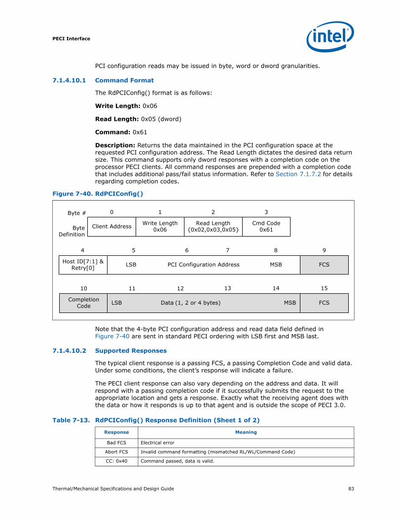
Thermal/Mechanical Specifications and Design Guide 83
PECI Interface
PCI configuration reads may be issued in byte, word or dword granularities.
7.1.4.10.1 Command Format
The RdPCIConfig() format is as follows:
Write Length: 0x06
Read Length: 0x05 (dword)
Command: 0x61
Description: Returns the data maintained in the PCI configuration space at the requested PCI configuration address. The Read Length dictates the desired data return size. This command supports only dword responses with a completion code on the processor PECI clients. All command responses are prepended with a completion code that includes additional pass/fail status information. Refer to Section 7.1.7.2 for details regarding completion codes.
Note that the 4-byte PCI configuration address and read data field defined in Figure 7-40 are sent in standard PECI ordering with LSB first and MSB last.
7.1.4.10.2 Supported Responses
The typical client response is a passing FCS, a passing Completion Code and valid data. Under some conditions, the client’s response will indicate a failure.
The PECI client response can also vary depending on the address and data. It will respond with a passing completion code if it successfully submits the request to the appropriate location and gets a response. Exactly what the receiving agent does with the data or how it responds is up to that agent and is outside the scope of PECI 3.0.
Figure 7-40. RdPCIConfig()
Byte Definition
0
Client Address
1
Write Length0x06
2
Read Length{0x02,0x03,0x05}
8
FCS
3
Cmd Code0x61
10
CompletionCode
11 13
FCS
4 5 76
LSB MSBPCI Configuration AddressHost ID[7:1] & Retry[0]
9
LSB Data (1, 2 or 4 bytes) MSB
12 14 15
Byte #
Table 7-13. RdPCIConfig() Response Definition (Sheet 1 of 2)
Response Meaning
Bad FCS Electrical error
Abort FCS Invalid command formatting (mismatched RL/WL/Command Code)
CC: 0x40 Command passed, data is valid.

PECI Interface
84 Thermal/Mechanical Specifications and Design Guide
7.1.4.11 RdPCIConfigLocal()
The RdPCIConfigLocal() command provides sideband read access to the PCI configuration space that resides within the processor. The exact listing of supported devices, functions and registers can be found in the relevant sections of the Intel® Core™ i7 Processor Family for the LGA-2011 Socket Datasheet, Volume 2. PECI originators may conduct a device/function/register enumeration sweep of this space by issuing reads in the same manner that the BIOS would. A response of all 1s may indicate that the device/function/register is unimplemented even with a ‘passing’ completion code. PECI originators can access this space even prior to BIOS enumeration of the system buses.
PCI configuration addresses are constructed as shown in Figure 7-41. Under normal in-band procedures, the Bus number would be used to direct a read or write to the proper device. Since there is a one-to-one mapping between any given client address and the bus number, any request made with a bad Bus number is ignored and the client will respond with all ‘0’s and a ‘passing’ completion code. All accesses to Bus0, Device[0-7] and Bus1, Device[8-15] are decoded to registers within the processor.
CC: 0x80 Response timeout. The processor was not able to generate the required response in a timely fashion. Retry is appropriate.
CC: 0x81 Response timeout. The processor is not able to allocate resources for servicing this command at this time. Retry is appropriate.
CC: 0x82 The processor hardware resources required to service this command are in a low power state. Retry may be appropriate after modification of PECI wake mode behavior if appropriate.
CC: 0x90 Unknown/Invalid Request
CC: 0x91 PECI control hardware, firmware or associated logic error. The processor is unable to process the request.
Table 7-13. RdPCIConfig() Response Definition (Sheet 2 of 2)
Response Meaning
Figure 7-41. PCI Configuration Address for Local Accesses
20 19 15 1114 12 023
DeviceBus Function Register
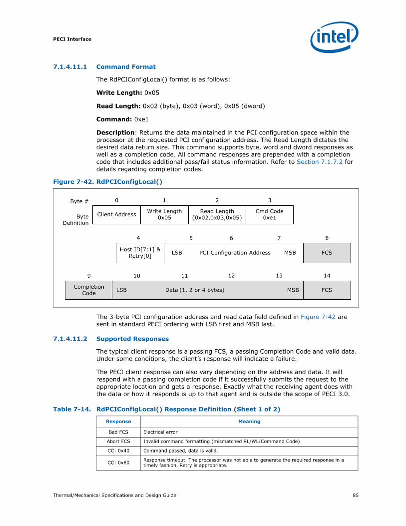
Thermal/Mechanical Specifications and Design Guide 85
PECI Interface
7.1.4.11.1 Command Format
The RdPCIConfigLocal() format is as follows:
Write Length: 0x05
Read Length: 0x02 (byte), 0x03 (word), 0x05 (dword)
Command: 0xe1
Description: Returns the data maintained in the PCI configuration space within the processor at the requested PCI configuration address. The Read Length dictates the desired data return size. This command supports byte, word and dword responses as well as a completion code. All command responses are prepended with a completion code that includes additional pass/fail status information. Refer to Section 7.1.7.2 for details regarding completion codes.
The 3-byte PCI configuration address and read data field defined in Figure 7-42 are sent in standard PECI ordering with LSB first and MSB last.
7.1.4.11.2 Supported Responses
The typical client response is a passing FCS, a passing Completion Code and valid data. Under some conditions, the client’s response will indicate a failure.
The PECI client response can also vary depending on the address and data. It will respond with a passing completion code if it successfully submits the request to the appropriate location and gets a response. Exactly what the receiving agent does with the data or how it responds is up to that agent and is outside the scope of PECI 3.0.
Figure 7-42. RdPCIConfigLocal()
0 1 2 3Byte #
FCS
12
7
9
CompletionCode
LSB PCI Configuration Address MSB
10
Write Length0x05
LSB Data (1, 2 or 4 bytes) MSB
5
Cmd Code0xe1
14
Read Length{0x02,0x03,0x05}
6 8
Host ID[7:1] & Retry[0]
Client Address
13
4
11
FCS
Byte Definition
Table 7-14. RdPCIConfigLocal() Response Definition (Sheet 1 of 2)
Response Meaning
Bad FCS Electrical error
Abort FCS Invalid command formatting (mismatched RL/WL/Command Code)
CC: 0x40 Command passed, data is valid.
CC: 0x80 Response timeout. The processor was not able to generate the required response in a timely fashion. Retry is appropriate.
PECI Interface
86 Thermal/Mechanical Specifications and Design Guide
7.1.4.12 WrPCIConfigLocal()
The WrPCIConfigLocal() command provides sideband write access to the PCI configuration space that resides within the processor. PECI originators may conduct a device/function/register enumeration sweep of this space by issuing reads in the same manner that BIOS would. PECI originators can access this space even before BIOS enumeration of the system buses. The exact listing of supported devices and functions for writes using this command on the processor is defined in Table 7-20.
Because a WrPCIConfigLocal() command results in an update to potentially critical registers inside the processor, it includes an Assured Write FCS (AW FCS) byte as part of the write data payload. In the event that the AW FCS mismatches with the client-calculated FCS, the client will abort the write and will always respond with a bad write FCS.
PCI Configuration addresses are constructed as shown in Figure 7-41. The write command is subject to the same address configuration rules as defined in Section 7.1.4.11. PCI configuration writes may be issued in byte, word or dword granularity.
7.1.4.12.1 Command Format
The WrPCIConfigLocal() format is as follows:
Write Length: 0x07 (byte), 0x08 (word), 0x0a (dword)
Read Length: 0x01
Command: 0xE5
AW FCS Support: Yes
Description: Writes the data sent to the requested register address. Write Length dictates the desired write granularity. The command always returns a completion code indicating pass/fail status. Refer to Section 7.1.7.2 for details on completion codes.
CC: 0x81 Response timeout. The processor is not able to allocate resources for servicing this command at this time. Retry is appropriate.
CC: 0x82The processor hardware resources required to service this command are in a low power state. Retry may be appropriate after modification of PECI wake mode behavior if appropriate.
CC: 0x90 Unknown/Invalid Request
CC: 0x91 PECI control hardware, firmware or associated logic error. The processor is unable to process the request.
Table 7-14. RdPCIConfigLocal() Response Definition (Sheet 2 of 2)
Response Meaning

Thermal/Mechanical Specifications and Design Guide 87
PECI Interface
The 3-byte PCI configuration address and write data field defined in Figure 7-43 are sent in standard PECI ordering with LSB first and MSB last.
7.1.4.12.2 Supported Responses
The typical client response is a passing FCS, a passing Completion Code and valid data. Under some conditions, the client’s response will indicate a failure.
The PECI client response can also vary depending on the address and data. It will respond with a passing completion code if it successfully submits the request to the appropriate location and gets a response. Exactly what the receiving agent does with the data or how it responds is up to that agent and is outside the scope of PECI 3.0.
Figure 7-43. WrPCIConfigLocal()
Byte Definition
0 1 2
FCS
3
CompletionCodeAW FCS
12
Byte #
FCS
13 14 15
Write Length{0x07, 0x08, 0x0a}
Host ID[7:1] & Retry[0]
4
8
Read Length0x01
5 6
Cmd Code0xe5
10 11
Client Address
9
LSB PCI Configuration Address MSB
LSB Data (1, 2 or 4 bytes) MSB
7
Table 7-15. WrPCIConfigLocal() Response Definition
Response Meaning
Bad FCS Electrical error or AW FCS failure
Abort FCS Invalid command formatting (mismatched RL/WL/Command Code)
CC: 0x40 Command passed, data is valid.
CC: 0x80 Response timeout. The processor was not able to generate the required response in a timely fashion. Retry is appropriate.
CC: 0x81 Response timeout. The processor is not able to allocate resources for servicing this command at this time. Retry is appropriate.
CC: 0x82The processor hardware resources required to service this command are in a low power state. Retry may be appropriate after modification of PECI wake mode behavior if appropriate.
CC: 0x90 Unknown/Invalid Request
CC: 0x91 PECI control hardware, firmware or associated logic error. The processor is unable to process the request.
PECI Interface
88 Thermal/Mechanical Specifications and Design Guide
7.1.4.12.3 WrPCIConfigLocal() Capabilities
On the processor PECI clients, the PECI WrPCIConfigLocal() command provides a method for programming certain memory controller functions as described in Table 7-16. Refer to the Intel® Core™ i7 Processor Family for the LGA-2011 Socket Datasheet, Volume 2 for more details on specific register definitions. It also enables writing to processor REUT (Robust Electrical Unified Test) registers associated with the Intel® QPI, PCIe* and DDR3 functions.
7.1.5 Client Management
7.1.5.1 Power-up Sequencing
The PECI client will not be available when the PWRGOOD signal is de-asserted. Any transactions on the bus during this time will be completely ignored, and the host will read the response from the client as all zeroes. PECI client initialization is completed approximately 100µS after the PWRGOOD assertion. This is represented by the start of the PECI Client “Data Not Ready” (DNR) phase in Figure 7-44. While in this phase, the PECI client will respond normally to the Ping() and GetDIB() commands and return the highest processor die temperature of 0x0000 to the GetTemp() command. All other commands will get a ‘Response Timeout’ completion in the DNR phase as shown in Table 7-17. All PECI services with the exception of core MSR space accesses become available ~500 uS after RESET_N de-assertion as shown in Figure 7-44. PECI will be fully functional with all services including core accesses being available when the core comes out of reset upon completion of the RESET ucode execution.
Table 7-16. WrPCIConfigLocal() Memory Controller Device/Function Support
Device Function Offset Range Description
15 0 104h-127h Integrated Memory Controller MemHot Registers
15 0 180h-1AFh Integrated Memory Controller SMBus Registers
16 0, 1, 4, 5 104h-18Bh1F4h-1FFh
Integrated Memory Controller Thermal Control Registers
16 2, 3, 6, 7 104h-147h Integrated Memory Controller Error Registers
Table 7-17. PECI Client Response During Power-Up
Command Response During ‘Data Not Ready’
Response During‘Available Except Core
Services’
Ping() Fully functional Fully functional
GetDIB() Fully functional Fully functional
GetTemp() Client responds with a ‘hot’ reading, or 0x0000 Fully functional
RdPkgConfig() Client responds with a timeout completion code of 0x81 Fully functional
WrPkgConfig() Client responds with a timeout completion code of 0x81 Fully functional
RdIAMSR() Client responds with a timeout completion code of 0x81 Client responds with a timeout completion code of 0x81
RdPCIConfigLocal() Client responds with a timeout completion code of 0x81 Fully functional
WrPCIConfigLocal() Client responds with a timeout completion code of 0x81 Fully functional
RdPCIConfig() Client responds with a timeout completion code of 0x81 Fully functional
WrPCIConfig() Client responds with a timeout completion code of 0x81 Fully functional
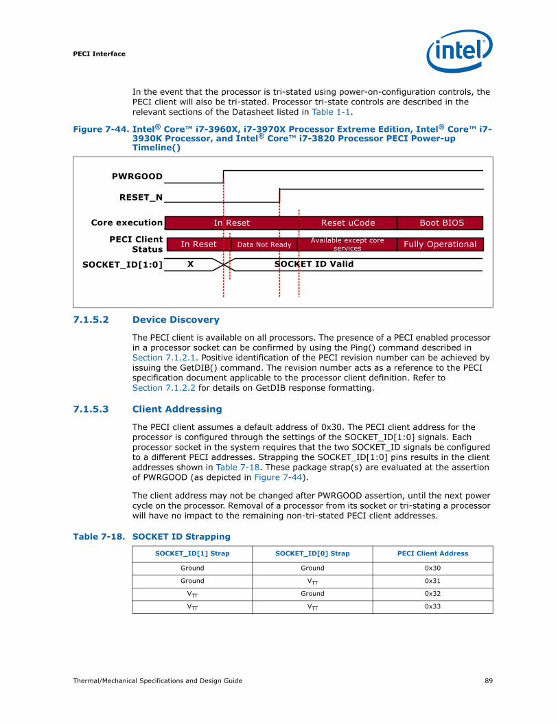
Thermal/Mechanical Specifications and Design Guide 89
PECI Interface
In the event that the processor is tri-stated using power-on-configuration controls, the PECI client will also be tri-stated. Processor tri-state controls are described in the relevant sections of the Datasheet listed in Table 1-1.
7.1.5.2 Device Discovery
The PECI client is available on all processors. The presence of a PECI enabled processor in a processor socket can be confirmed by using the Ping() command described in Section 7.1.2.1. Positive identification of the PECI revision number can be achieved by issuing the GetDIB() command. The revision number acts as a reference to the PECI specification document applicable to the processor client definition. Refer to Section 7.1.2.2 for details on GetDIB response formatting.
7.1.5.3 Client Addressing
The PECI client assumes a default address of 0x30. The PECI client address for the processor is configured through the settings of the SOCKET_ID[1:0] signals. Each processor socket in the system requires that the two SOCKET_ID signals be configured to a different PECI addresses. Strapping the SOCKET_ID[1:0] pins results in the client addresses shown in Table 7-18. These package strap(s) are evaluated at the assertion of PWRGOOD (as depicted in Figure 7-44).
The client address may not be changed after PWRGOOD assertion, until the next power cycle on the processor. Removal of a processor from its socket or tri-stating a processor will have no impact to the remaining non-tri-stated PECI client addresses.
Figure 7-44. Intel® Core™ i7-3960X, i7-3970X Processor Extreme Edition, Intel® Core™ i7-3930K Processor, and Intel® Core™ i7-3820 Processor PECI Power-up Timeline()
PWRGOOD
RESET_N
Core execution idle runningReset uCode Boot BIOS
PECI Client Status Data Not Ready Available except core
services
SOCKET_ID[1:0] X SOCKET ID Valid
In Reset
Fully OperationalIn Reset
Table 7-18. SOCKET ID Strapping
SOCKET_ID[1] Strap SOCKET_ID[0] Strap PECI Client Address
Ground Ground 0x30
Ground VTT 0x31
VTT Ground 0x32
VTT VTT 0x33
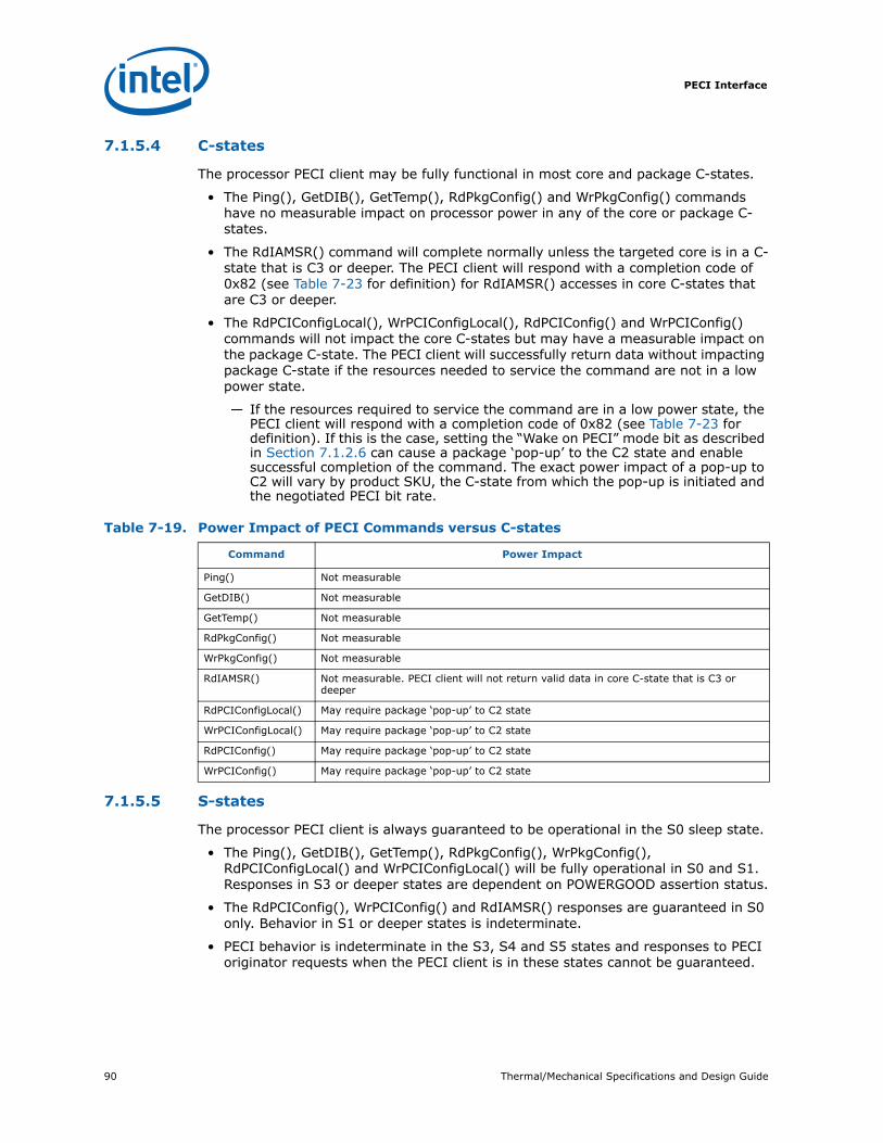
PECI Interface
90 Thermal/Mechanical Specifications and Design Guide
7.1.5.4 C-states
The processor PECI client may be fully functional in most core and package C-states.
• The Ping(), GetDIB(), GetTemp(), RdPkgConfig() and WrPkgConfig() commands have no measurable impact on processor power in any of the core or package C-states.
• The RdIAMSR() command will complete normally unless the targeted core is in a C-state that is C3 or deeper. The PECI client will respond with a completion code of 0x82 (see Table 7-23 for definition) for RdIAMSR() accesses in core C-states that are C3 or deeper.
• The RdPCIConfigLocal(), WrPCIConfigLocal(), RdPCIConfig() and WrPCIConfig() commands will not impact the core C-states but may have a measurable impact on the package C-state. The PECI client will successfully return data without impacting package C-state if the resources needed to service the command are not in a low power state.
— If the resources required to service the command are in a low power state, the PECI client will respond with a completion code of 0x82 (see Table 7-23 for definition). If this is the case, setting the “Wake on PECI” mode bit as described in Section 7.1.2.6 can cause a package ‘pop-up’ to the C2 state and enable successful completion of the command. The exact power impact of a pop-up to C2 will vary by product SKU, the C-state from which the pop-up is initiated and the negotiated PECI bit rate.
7.1.5.5 S-states
The processor PECI client is always guaranteed to be operational in the S0 sleep state.
• The Ping(), GetDIB(), GetTemp(), RdPkgConfig(), WrPkgConfig(), RdPCIConfigLocal() and WrPCIConfigLocal() will be fully operational in S0 and S1. Responses in S3 or deeper states are dependent on POWERGOOD assertion status.
• The RdPCIConfig(), WrPCIConfig() and RdIAMSR() responses are guaranteed in S0 only. Behavior in S1 or deeper states is indeterminate.
• PECI behavior is indeterminate in the S3, S4 and S5 states and responses to PECI originator requests when the PECI client is in these states cannot be guaranteed.
Table 7-19. Power Impact of PECI Commands versus C-states
Command Power Impact
Ping() Not measurable
GetDIB() Not measurable
GetTemp() Not measurable
RdPkgConfig() Not measurable
WrPkgConfig() Not measurable
RdIAMSR() Not measurable. PECI client will not return valid data in core C-state that is C3 or deeper
RdPCIConfigLocal() May require package ‘pop-up’ to C2 state
WrPCIConfigLocal() May require package ‘pop-up’ to C2 state
RdPCIConfig() May require package ‘pop-up’ to C2 state
WrPCIConfig() May require package ‘pop-up’ to C2 state

Thermal/Mechanical Specifications and Design Guide 91
PECI Interface
7.1.5.6 Processor Reset
The processor PECI client is fully reset on all RESET_N assertions. Upon deassertion of RESET_N where power is maintained to the processor (otherwise known as a ‘warm reset’), the following are true:
• The PECI client assumes a bus Idle state.
• The Thermal Filtering Constant is retained.
• PECI SOCKET_ID is retained.
• GetTemp() reading resets to 0x0000.
• Any transaction in progress is aborted by the client (as measured by the client no longer participating in the response).
• The processor client is otherwise reset to a default configuration.
7.1.5.7 Processor Error Handling
Availability of PECI services may be affected by the processor PECI client error status. Server manageability requirements place a strong emphasis on continued availability of PECI services to facilitate logging and debug of the error condition.
• Most processor PECI client services are available in the event of a CATERR_N assertion though they cannot be guaranteed.
• The Ping(), GetDIB(), GetTemp(), RdPkgConfig() and WrPkgConfig() commands will be serviced if the source of the CATERR_N assertion is not in the processor power control unit hardware, firmware or associated register logic. Additionally, the RdPCIConfigLocal() and WrPCIConfigLocal() commands may also be serviced in this case.
• It is recommended that the PECI originator read Index 0/Parameter 5 using the RdPkgConfig() command to debug the CATERR_N assertion.
— The PECI client will return the 0x91 completion code if the CATERR_N assertion is caused by the PECI control hardware, firmware or associated logic errors. In such an event, only the Ping(), GetTemp() and GetDIB() PECI commands may be serviced. All other processor PECI services will be unavailable and further debug of the processor error status will not be possible.
— If the PECI client returns a passing completion code, the originator should use the response data to determine the cause of the CATERR_N assertion. In such an event, it is also recommended that the PECI originator determine the exact suite of available PECI client services by issuing each of the PECI commands. The processor will issue ‘timeout’ responses for those services that may not be available.
— If the PECI client continues to return the 0x81 completion code in response to multiple retries of the RdPkgConfig() command, no PECI services, with the exception of the Ping(), GetTemp() and GetDIB(), will be guaranteed.
• The RdIAMSR() command may be serviced during a CATERR_N assertion though it cannot be guaranteed.
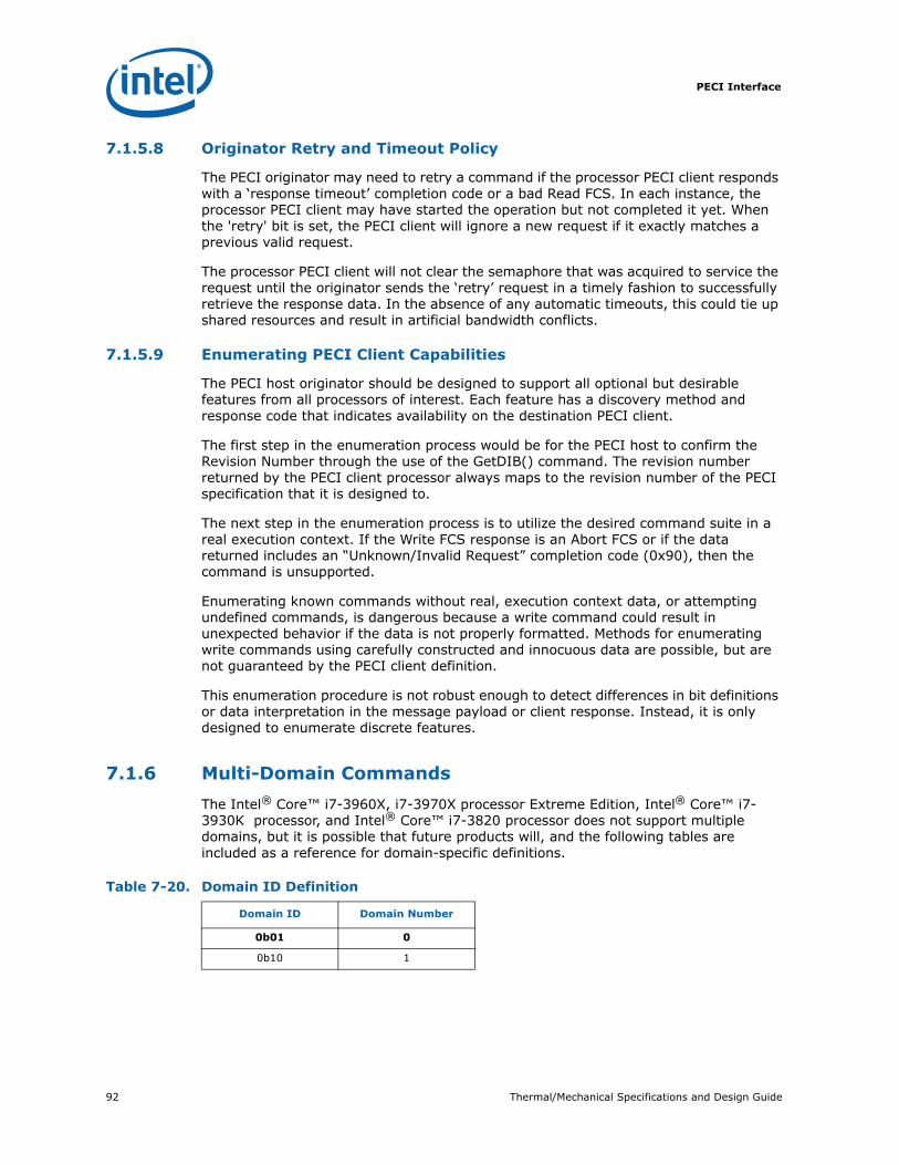
PECI Interface
92 Thermal/Mechanical Specifications and Design Guide
7.1.5.8 Originator Retry and Timeout Policy
The PECI originator may need to retry a command if the processor PECI client responds with a ‘response timeout’ completion code or a bad Read FCS. In each instance, the processor PECI client may have started the operation but not completed it yet. When the 'retry' bit is set, the PECI client will ignore a new request if it exactly matches a previous valid request.
The processor PECI client will not clear the semaphore that was acquired to service the request until the originator sends the ‘retry’ request in a timely fashion to successfully retrieve the response data. In the absence of any automatic timeouts, this could tie up shared resources and result in artificial bandwidth conflicts.
7.1.5.9 Enumerating PECI Client Capabilities
The PECI host originator should be designed to support all optional but desirable features from all processors of interest. Each feature has a discovery method and response code that indicates availability on the destination PECI client.
The first step in the enumeration process would be for the PECI host to confirm the Revision Number through the use of the GetDIB() command. The revision number returned by the PECI client processor always maps to the revision number of the PECI specification that it is designed to.
The next step in the enumeration process is to utilize the desired command suite in a real execution context. If the Write FCS response is an Abort FCS or if the data returned includes an “Unknown/Invalid Request” completion code (0x90), then the command is unsupported.
Enumerating known commands without real, execution context data, or attempting undefined commands, is dangerous because a write command could result in unexpected behavior if the data is not properly formatted. Methods for enumerating write commands using carefully constructed and innocuous data are possible, but are not guaranteed by the PECI client definition.
This enumeration procedure is not robust enough to detect differences in bit definitions or data interpretation in the message payload or client response. Instead, it is only designed to enumerate discrete features.
7.1.6 Multi-Domain CommandsThe Intel® Core™ i7-3960X, i7-3970X processor Extreme Edition, Intel® Core™ i7-3930K processor, and Intel® Core™ i7-3820 processor does not support multiple domains, but it is possible that future products will, and the following tables are included as a reference for domain-specific definitions.
Table 7-20. Domain ID Definition
Domain ID Domain Number
0b01 0
0b10 1
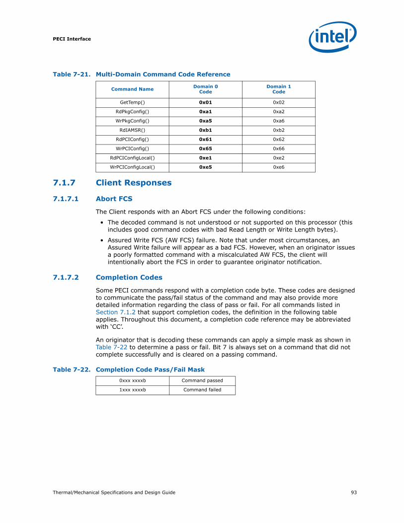
Thermal/Mechanical Specifications and Design Guide 93
PECI Interface
7.1.7 Client Responses
7.1.7.1 Abort FCS
The Client responds with an Abort FCS under the following conditions:
• The decoded command is not understood or not supported on this processor (this includes good command codes with bad Read Length or Write Length bytes).
• Assured Write FCS (AW FCS) failure. Note that under most circumstances, an Assured Write failure will appear as a bad FCS. However, when an originator issues a poorly formatted command with a miscalculated AW FCS, the client will intentionally abort the FCS in order to guarantee originator notification.
7.1.7.2 Completion Codes
Some PECI commands respond with a completion code byte. These codes are designed to communicate the pass/fail status of the command and may also provide more detailed information regarding the class of pass or fail. For all commands listed in Section 7.1.2 that support completion codes, the definition in the following table applies. Throughout this document, a completion code reference may be abbreviated with ‘CC’.
An originator that is decoding these commands can apply a simple mask as shown in Table 7-22 to determine a pass or fail. Bit 7 is always set on a command that did not complete successfully and is cleared on a passing command.
Table 7-21. Multi-Domain Command Code Reference
Command Name Domain 0Code
Domain 1Code
GetTemp() 0x01 0x02
RdPkgConfig() 0xa1 0xa2
WrPkgConfig() 0xa5 0xa6
RdIAMSR() 0xb1 0xb2
RdPCIConfig() 0x61 0x62
WrPCIConfig() 0x65 0x66
RdPCIConfigLocal() 0xe1 0xe2
WrPCIConfigLocal() 0xe5 0xe6
Table 7-22. Completion Code Pass/Fail Mask
0xxx xxxxb Command passed
1xxx xxxxb Command failed
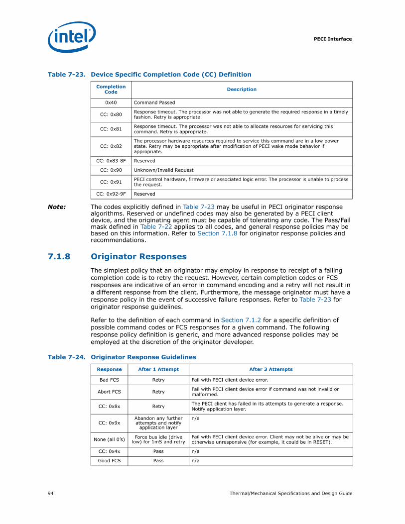
PECI Interface
94 Thermal/Mechanical Specifications and Design Guide
Note: The codes explicitly defined in Table 7-23 may be useful in PECI originator response algorithms. Reserved or undefined codes may also be generated by a PECI client device, and the originating agent must be capable of tolerating any code. The Pass/Fail mask defined in Table 7-22 applies to all codes, and general response policies may be based on this information. Refer to Section 7.1.8 for originator response policies and recommendations.
7.1.8 Originator ResponsesThe simplest policy that an originator may employ in response to receipt of a failing completion code is to retry the request. However, certain completion codes or FCS responses are indicative of an error in command encoding and a retry will not result in a different response from the client. Furthermore, the message originator must have a response policy in the event of successive failure responses. Refer to Table 7-23 for originator response guidelines.
Refer to the definition of each command in Section 7.1.2 for a specific definition of possible command codes or FCS responses for a given command. The following response policy definition is generic, and more advanced response policies may be employed at the discretion of the originator developer.
Table 7-23. Device Specific Completion Code (CC) Definition
CompletionCode Description
0x40 Command Passed
CC: 0x80 Response timeout. The processor was not able to generate the required response in a timely fashion. Retry is appropriate.
CC: 0x81 Response timeout. The processor was not able to allocate resources for servicing this command. Retry is appropriate.
CC: 0x82The processor hardware resources required to service this command are in a low power state. Retry may be appropriate after modification of PECI wake mode behavior if appropriate.
CC: 0x83-8F Reserved
CC: 0x90 Unknown/Invalid Request
CC: 0x91 PECI control hardware, firmware or associated logic error. The processor is unable to process the request.
CC: 0x92-9F Reserved
Table 7-24. Originator Response Guidelines
Response After 1 Attempt After 3 Attempts
Bad FCS Retry Fail with PECI client device error.
Abort FCS Retry Fail with PECI client device error if command was not invalid or malformed.
CC: 0x8x Retry The PECI client has failed in its attempts to generate a response. Notify application layer.
CC: 0x9xAbandon any further attempts and notify
application layer
n/a
None (all 0’s) Force bus idle (drive low) for 1mS and retry
Fail with PECI client device error. Client may not be alive or may be otherwise unresponsive (for example, it could be in RESET).
CC: 0x4x Pass n/a
Good FCS Pass n/a
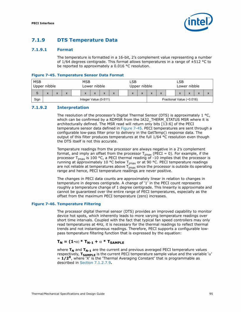
Thermal/Mechanical Specifications and Design Guide 95
PECI Interface
7.1.9 DTS Temperature Data
7.1.9.1 Format
The temperature is formatted in a 16-bit, 2’s complement value representing a number of 1/64 degrees centigrade. This format allows temperatures in a range of ±512 °C to be reported to approximately a 0.016 °C resolution.
7.1.9.2 Interpretation
The resolution of the processor’s Digital Thermal Sensor (DTS) is approximately 1 °C, which can be confirmed by a RDMSR from the IA32_THERM_STATUS MSR where it is architecturally defined. The MSR read will return only bits [13:6] of the PECI temperature sensor data defined in Figure 7-45. PECI temperatures are sent through a configurable low-pass filter prior to delivery in the GetTemp() response data. The output of this filter produces temperatures at the full 1/64 °C resolution even though the DTS itself is not this accurate.
Temperature readings from the processor are always negative in a 2’s complement format, and imply an offset from the processor Tjmax (PECI = 0). For example, if the processor Tjmax is 100 °C, a PECI thermal reading of -10 implies that the processor is running at approximately 10 °C below Tjmax or at 90 °C. PECI temperature readings are not reliable at temperatures above Tjmax since the processor is outside its operating range and hence, PECI temperature readings are never positive.
The changes in PECI data counts are approximately linear in relation to changes in temperature in degrees centigrade. A change of ‘1’ in the PECI count represents roughly a temperature change of 1 degree centigrade. This linearity is approximate and cannot be guaranteed over the entire range of PECI temperatures, especially as the offset from the maximum PECI temperature (zero) increases.
Figure 7-46. Temperature Filtering
The processor digital thermal sensor (DTS) provides an improved capability to monitor device hot spots, which inherently leads to more varying temperature readings over short time intervals. Coupled with the fact that typical fan speed controllers may only read temperatures at 4Hz, it is necessary for the thermal readings to reflect thermal trends and not instantaneous readings. Therefore, PECI supports a configurable low-pass temperature filtering function that is expressed by the equation:
TN = (1-α) * TN-1 + α * TSAMPLE
where TN and TN-1 are the current and previous averaged PECI temperature values respectively, TSAMPLE is the current PECI temperature sample value and the variable ‘α’ = 1/2X, where ‘X’ is the ‘Thermal Averaging Constant’ that is programmable as described in Section 7.1.2.7.9.
Figure 7-45. Temperature Sensor Data Format
MSBUpper nibble
MSBLower nibble
LSBUpper nibble
LSBLower nibble
S x x x x x x x x x x x x x x x
Sign Integer Value (0-511) Fractional Value (~0.016)

PECI Interface
96 Thermal/Mechanical Specifications and Design Guide
7.1.9.3 Reserved Values
Several values well out of the operational range are reserved to signal temperature sensor errors. These are summarized in Table 7-25.
§
Table 7-25. Error Codes and Descriptions
Error Code Description
0x8000 General Sensor Error (GSE)
0x8001 Reserved
0x8002 Sensor is operational, but has detected a temperature below its operational range (underflow)
0x8003-0x81ff Reserved
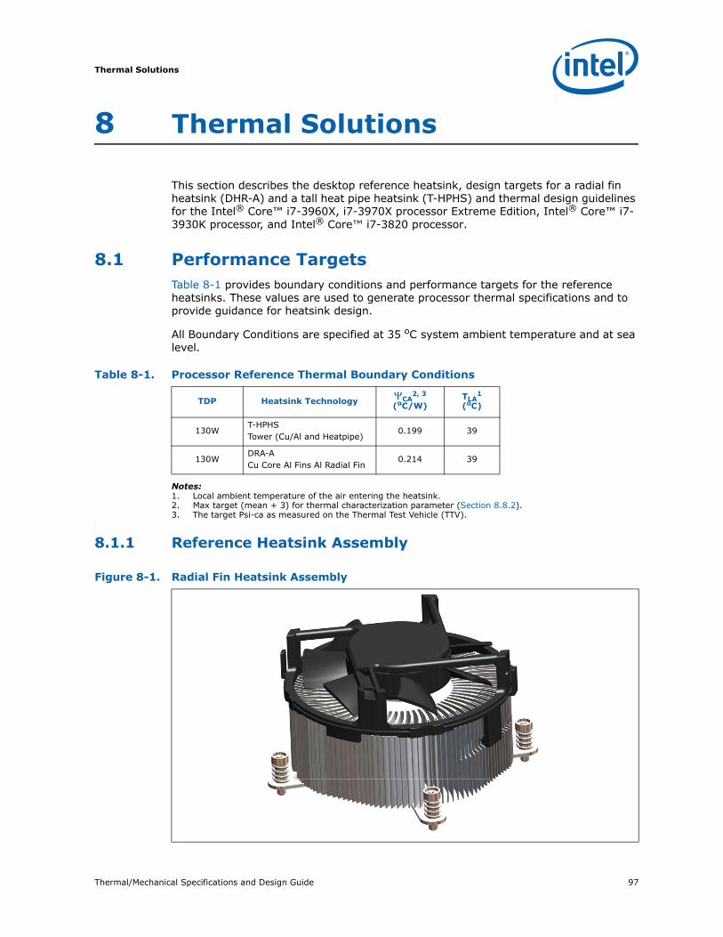
Thermal/Mechanical Specifications and Design Guide 97
Thermal Solutions
8 Thermal Solutions
This section describes the desktop reference heatsink, design targets for a radial fin heatsink (DHR-A) and a tall heat pipe heatsink (T-HPHS) and thermal design guidelines for the Intel® Core™ i7-3960X, i7-3970X processor Extreme Edition, Intel® Core™ i7-3930K processor, and Intel® Core™ i7-3820 processor.
8.1 Performance TargetsTable 8-1 provides boundary conditions and performance targets for the reference heatsinks. These values are used to generate processor thermal specifications and to provide guidance for heatsink design.
All Boundary Conditions are specified at 35 oC system ambient temperature and at sea level.
Notes:1. Local ambient temperature of the air entering the heatsink.2. Max target (mean + 3) for thermal characterization parameter (Section 8.8.2). 3. The target Psi-ca as measured on the Thermal Test Vehicle (TTV).
,
8.1.1 Reference Heatsink Assembly
Table 8-1. Processor Reference Thermal Boundary Conditions
TDP Heatsink Technology ΨCA2, 3
(oC/W)TLA
1
(oC)
130WT-HPHSTower (Cu/Al and Heatpipe)
0.199 39
130WDRA-ACu Core Al Fins Al Radial Fin
0.214 39
Figure 8-1. Radial Fin Heatsink Assembly

Thermal Solutions
98 Thermal/Mechanical Specifications and Design Guide
8.2 Assembly Process for Reference HeatsinksUnless noted the assembly process covers both the radial fin and Tall Heat Pipe Heat Sink (T-HPHS). Compliance to Board Keepout Zones in Appendix A is assumed for this assembly process.
• Remove thermal solution from packaging.
— T-HPHS only: remove fan guard.• Remove protective cover from TIM and inspect pre-applied TIM for damage.
• Position the thermal solution over the processor. Align/seat retention screw/mounting bracket with ILM studs. The thermal solution should seat on the studs while not contacting the processor package.
— T-HPHS only: The heatsink assembly must be properly orientated for proper air flow. Consult motherboard documentation, for recommendation.
• Engage each of the 4 retention screws by 1-2 turns following a cross pattern. This ensures that none of the screws are cross-threaded and provides for easier installation by preventing heatsink from tilting.
— Cross-threading of retention screws will damage the ILM requiring ILM replacement Align the four captive screws of the heatsink to the four threaded studs of the back plate.
— T-HPHS only: The rear screws, on side opposite of the fan, are accessed through the holes in the heatsink fin stack.
• Using a #2 Phillips driver, torque the four captive screws to 8 inch-pounds. Tighten a cross pattern.
• T-HPHS only: reinstall the fan guard.
• Attach the fan wire connector to the 4 pin fan header connector on the motherboard labeled Processor FAN. Consult the motherboard documentation for proper fan connection.
Figure 8-2. Tall Heat Pipe Heatsink Assembly
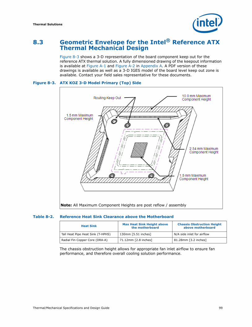
Thermal/Mechanical Specifications and Design Guide 99
Thermal Solutions
8.3 Geometric Envelope for the Intel® Reference ATX Thermal Mechanical DesignFigure 8-3 shows a 3-D representation of the board component keep out for the reference ATX thermal solution. A fully dimensioned drawing of the keepout information is available at Figure A-1 and Figure A-2 in Appendix A. A PDF version of these drawings is available as well as a 3-D IGES model of the board level keep out zone is available. Contact your field sales representative for these documents.
The chassis obstruction height allows for appropriate fan inlet airflow to ensure fan performance, and therefore overall cooling solution performance.
Figure 8-3. ATX KOZ 3-D Model Primary (Top) Side
Note: All Maximum Component Heights are post reflow / assembly
Table 8-2. Reference Heat Sink Clearance above the Motherboard
Heat Sink Max Heat Sink Height above the motherboard
Chassis Obstruction Height above motherboard
Tall Heat Pipe Heat Sink (T-HPHS) 130mm [5.51 inches] N/A side inlet for airflow
Radial Fin Copper Core (DRA-A) 71.12mm [2.8 inches] 81.28mm [3.2 inches]

Thermal Solutions
100 Thermal/Mechanical Specifications and Design Guide
8.4 Structural ConsiderationsMass of the Tall Heat Pipe Heat Sink and the Radial Fin Copper core Heat Sink does not exceed 600 gm. The mass of the thermal solution includes all of the components, including the clip, springs and fasteners.
From Table 5-3, the Dynamic Compressive Load of 132 lbf max allows for designs that exceed 600 gm as long as the mathematical product does not exceed 132 lbf. The Total Static Compressive Load (Table 5-3) should also be considered in dynamic assessments.
8.5 Attachment to the ILMRefer to Figure 4-15 for the critical to function dimensions to attach a heatsink to the LGA2011 socket ILM.
8.6 Thermal Interface MaterialA thermal interface material (TIM) provides conductivity between the IHS and heat sink.
Table 8-3. Intel® Reference Thermal Solution TIM
Thermal Solution TIM
T-HPHSTower (Cu/Al and Heatpipe)
SHIN-ETSU G751 (reference) DOW TC-1996 (collaboration)
DRA-ACu Core Al Fins Al Radial Fin
DOW TC-1996
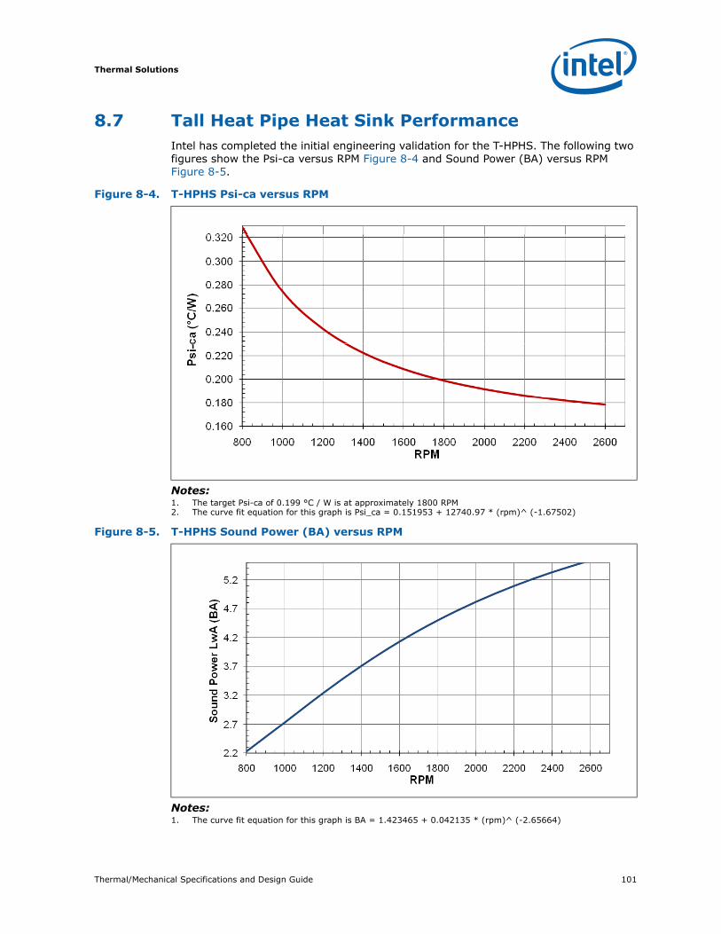
Thermal/Mechanical Specifications and Design Guide 101
Thermal Solutions
8.7 Tall Heat Pipe Heat Sink Performance Intel has completed the initial engineering validation for the T-HPHS. The following two figures show the Psi-ca versus RPM Figure 8-4 and Sound Power (BA) versus RPM Figure 8-5.
Notes:1. The target Psi-ca of 0.199 °C / W is at approximately 1800 RPM2. The curve fit equation for this graph is Psi_ca = 0.151953 + 12740.97 * (rpm)^ (-1.67502)
Notes:1. The curve fit equation for this graph is BA = 1.423465 + 0.042135 * (rpm)^ (-2.65664)
Figure 8-4. T-HPHS Psi-ca versus RPM
Figure 8-5. T-HPHS Sound Power (BA) versus RPM
Thermal Solutions
102 Thermal/Mechanical Specifications and Design Guide
8.8 Thermal Design Guidelines
8.8.1 Intel® Turbo Boost 2 TechnologyIntel Turbo Boost 2 Technology is a feature available on certain processor SKUs that opportunistically, and automatically, allows the processor to run faster than the marked frequency if the part is operating below its power, temperature and current limits.
Heatsink performance (lower ΨCA as described in Section 6.1.3) is one of several factors that can impact the amount of Turbo Mode frequency benefit. Turbo Mode performance is also constrained by ICC, and VCC limits.
With Turbo Mode enabled, the processor may run more consistently at higher power levels (but still within TDP), and be more likely to operate above TCONTROL, as compared to when Turbo Mode is disabled. This may result in higher acoustics.
8.8.2 Thermal Characterization ParameterThe case-to-local ambient Thermal Characterization Parameter (ΨCA) is defined by:
Equation 8-1.
ΨCA = (TTTV-CASE - TLA) / TDP
Where:TTTV-CASE= Thermal Test Vehicle (TTV) case temperature (°C). For TTTV-CASE
specification see Section 6.1.1.TLA = Local ambient temperature in chassis at processor thermal solution
inlet (°C).TDP = TDP (W) assumes all power dissipates through the integrated heat
spreader of the TTV. The TTV thermal profile see Figure 6-1 and Table 6-2 account for differences in temperature distribution between processor and TTV. No user correction is required
Εθυατιον 8 2.
ΨCA = ΨCS + ΨSA
Where:ΨCS = Thermal characterization parameter of the TIM (°C/W) is dependent
on the thermal conductivity and thickness of the TIM.ΨSA = Thermal characterization parameter from heatsink-to-local ambient
(°C/W) is dependent on the thermal conductivity and geometry of the heatsink and dependent on the air velocity through the heatsink fins.
Figure 8-6 illustrates the thermal characterization parameters.
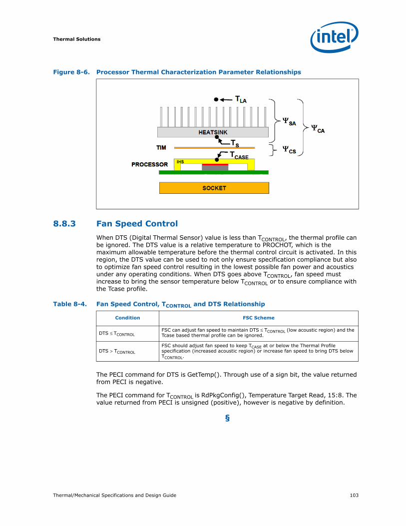
Thermal/Mechanical Specifications and Design Guide 103
Thermal Solutions
8.8.3 Fan Speed ControlWhen DTS (Digital Thermal Sensor) value is less than TCONTROL, the thermal profile can be ignored. The DTS value is a relative temperature to PROCHOT, which is the maximum allowable temperature before the thermal control circuit is activated. In this region, the DTS value can be used to not only ensure specification compliance but also to optimize fan speed control resulting in the lowest possible fan power and acoustics under any operating conditions. When DTS goes above TCONTROL, fan speed must increase to bring the sensor temperature below TCONTROL or to ensure compliance with the Tcase profile.
The PECI command for DTS is GetTemp(). Through use of a sign bit, the value returned from PECI is negative.
The PECI command for TCONTROL is RdPkgConfig(), Temperature Target Read, 15:8. The value returned from PECI is unsigned (positive), however is negative by definition.
§
Figure 8-6. Processor Thermal Characterization Parameter Relationships
Table 8-4. Fan Speed Control, TCONTROL and DTS Relationship
Condition FSC Scheme
DTS ≤ TCONTROLFSC can adjust fan speed to maintain DTS ≤ TCONTROL (low acoustic region) and the Tcase based thermal profile can be ignored.
DTS > TCONTROL
FSC should adjust fan speed to keep TCASE at or below the Thermal Profile specification (increased acoustic region) or increase fan speed to bring DTS below TCONTROL.

Thermal Solutions
104 Thermal/Mechanical Specifications and Design Guide
Thermal/Mechanical Specifications and Design Guide 105
Quality and Reliability Requirements
9 Quality and Reliability Requirements
9.1 Use ConditionsIntel evaluates reliability performance based on the use conditions (operating environment) of the end product by using acceleration models.
The use condition environment definitions provided in Table 9-1 and Table 9-2 are based on speculative use condition assumptions, and are provided as examples only.
Based on the system enabling boundary condition, the solder ball temperature can vary and needs to be comprehended for reliability assessment.
Table 9-1. Use Conditions Environment (System Level)
Use Environment Speculative Stress Condition
Example Use Condition
Example 7-Yr Stress Equiv.
Example 10-Yr Stress Equiv.
Slow small internal gradient changes due to external ambient (temperature cycle or externally heated)Fast, large gradient on/off to max operating temp.(power cycle or internally heated including power save features)
Temperature Cycle DT = 35–44 °C(solder joint)
550–930 cyclesTemp Cycle
(-25 °C to 100 °C)
780–1345 cyclesTemp Cycle
(-25 °C to 100 °C)
High ambient moisture during low-power state (operating voltage)
THB/HASTT = 25–30 °C
85%RH(ambient)
110–220 hrs at110 °C 85%RH
145–240 hrs at 110 °C 85%RH
High Operating temperature and short duration high temperature exposures
Bake T = 95–105 °C(contact)
700–2500 hrs at125 °C
800–3300 hrs at125 °C
Quality and Reliability Requirements
106 Thermal/Mechanical Specifications and Design Guide
9.2 Intel® Reference Component ValidationIntel tests reference components individually and as an assembly on mechanical test boards and assesses performance to the envelopes specified in previous sections by varying boundary conditions.
While component validation shows a reference design is tenable for a limited range of conditions, customers need to assess their specific boundary conditions and perform reliability testing based on their use conditions.
Intel reference components are also used in board functional tests to assess performance for specific conditions.
9.2.1 Board Functional Test SequenceEach test sequence should start with components (baseboard, heatsink assembly, and so on) that have not been previously submitted to any reliability testing.
Prior to the mechanical shock & vibration test, the units under test should be preconditioned for 72 hours at 45 ºC. The purpose is to account for load relaxation during burn-in stage.
The test sequence should always start with a visual inspection after assembly, and BIOS/Processor/memory test. The stress test should be then followed by a visual inspection and then BIOS/Processor/memory test.
Table 9-2. Use Conditions Environment (System Level)
Use Environment Speculative Stress Condition Example Use Condition
Shipping and Handling
Mechanical Shock• System-level• Unpackaged• Trapezoidal• 25 g• velocity change is based on packaged weight
Total of 12 drops per system:• 2 drops per axis• ± direction
Product Weight (lbs) Non-palletized Product Velocity Change (in/sec)
< 20 lbs 20 to > 40 40 to > 80 80 to < 100 100 to < 120≥120
250225205175145125
Change in velocity is based upon a 0.5 coefficient of restitution.
Shipping and Handling
Random Vibration• System Level• Unpackaged• 5 Hz to 500 Hz• 2.20 g RMS random• 5 Hz @ 0.001 g2/Hz to 20 Hz @ 0.01 g2/Hz
(slope up)• 20 Hz to 500 Hz @ 0.01 g2/Hz (flat)• Random control limit tolerance is ± 3 dB
Total per system:• 10 minutes per axis• 3 axes
Thermal/Mechanical Specifications and Design Guide 107
Quality and Reliability Requirements
9.2.2 Post-Test Pass Criteria ExamplesThe post-test pass criteria examples are:1. No significant physical damage to the heatsink and retention hardware. 2. Heatsink remains seated and its bottom remains mated flat against the IHS
surface. No visible gap between the heatsink base and processor IHS. No visible tilt of the heatsink with respect to the retention hardware.
3. No signs of physical damage on baseboard surface due to impact of heatsink.4. No visible physical damage to the processor package.5. Successful BIOS/Processor/memory test of post-test samples.6. Thermal compliance testing to demonstrate that the case temperature specification
can be met.
9.2.3 Recommended BIOS/Processor/Memory Test ProceduresThis test is to ensure proper operation of the product before and after environmental stresses, with the thermal mechanical enabling components assembled. The test shall be conducted on a fully operational baseboard that has not been exposed to any battery of tests prior to the test being considered.
Testing setup should include the following components, properly assembled and/or connected:
• Appropriate system baseboard.• Processor and memory.• All enabling components, including socket and thermal solution parts.
The pass criterion is that the system under test shall successfully complete the checking of BIOS, basic processor functions and memory, without any errors. Intel PC Diags is an example of software that can be utilized for this test.
9.3 Material and Recycling RequirementsMaterial shall be resistant to fungal growth. Examples of non-resistant materials include cellulose materials, animal and vegetable based adhesives, grease, oils, and many hydrocarbons. Synthetic materials such as PVC formulations, certain polyurethane compositions (for example, polyester and some polyethers), plastics which contain organic fillers of laminating materials, paints, and varnishes also are susceptible to fungal growth. If materials are not fungal growth resistant, then MIL-STD-810E, Method 508.4 must be performed to determine material performance. Cadmium shall not be used in the painting or plating of the socket.CFCs and HFCs shall not be used in manufacturing the socket.
Any plastic component exceeding 25 gm should be recyclable per the European Blue Angel recycling standards.
Supplier is responsible for complying with industry standards regarding environmental care as well as with the specific standards required per Supplier's region. More specifically, Supplier is responsible for compliance with the European regulations related to restrictions on the use of Lead and Bromine containing flame-retardants. Legislation varies by geography, European Union (RoHS/WEEE), China, California, and so forth.

Quality and Reliability Requirements
108 Thermal/Mechanical Specifications and Design Guide
The following definitions apply to the use of the terms lead-free, Pb-free, and RoHS compliant:
Halogen flame retardant free (HFR-Free) PCB: In future revisionsof this document, Intel will be providing guidance on the mechanical impact to using a HFR-free laminate in the PCB.
Lead-free and Pb-free: Lead has not been intentionally added, but lead may still exist as an impurity below 1000 ppm.
RoHS compliant: Lead and other materials banned in RoHS Directive are either (1) below all applicable substance thresholds as proposed by the EU or (2) an approved/pending exemption applies.
Note: RoHS implementation details are not fully defined and may change.§
Thermal/Mechanical Specifications and Design Guide 109
Mechanical Drawings
A Mechanical Drawings
Table A-1 lists the Mechanical drawings included in this appendix.
Table A-1. Mechanical Drawing List
Description Figure
Board Keepin / Keepout Zones (Sheet 1 of 2) Figure A-1
Board Keepin / Keepout Zones (Sheet 2 of 2) Figure A-2
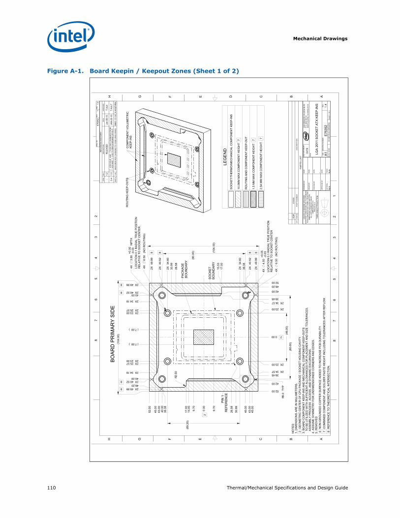
Mechanical Drawings
110 Thermal/Mechanical Specifications and Design Guide
Figure A-1. Board Keepin / Keepout Zones (Sheet 1 of 2)
8
7
6
5
4
3
2
H G F E D C B A
8
7
6
5
4
3
2
1
H G F E D C B A
R
52.00
0.00
39.45
2X 23.00
2X 23.00
39.45
42.00
52.00
52.0
0
0.00
45.0
0
9.70
9.70
R2.5
0 2X 34.57
2X 34.57
42.00
2X
849
.99
2X
840
.52
2X
840
.52
2X
849
.99
2X 23.00
2X 23.00
2X 3
4.60
2X 3
4.60
38.3
8
2X 8 49.99
2X 8 40.52
2X 8 40.52
2X 8 49.99
45.0
0
30.9
9
38.3
8
17.0
0
48.20
30.9
9
40.0
0
40.0
0
40.00
40.00
4X
(NO
RO
UTI
NG
)6.
50
4X
LOC
ATI
ON
0.1
RA
DIA
L TR
UE
PO
SIT
ION
RE
LATI
VE
TO
SO
CK
ET
CE
NTE
R
4.50
+0.0
5-0
.03
4X
(NO
RO
UTI
NG
)6.
50
R T
YP
5.0
17.0
0
2X 34.18
2X 34.18
48.20
43.0
0
43.0
0
26.5
8
14.4
5
26.5
8
15.5
3
2X 25.57
2X 25.57
4X
NP
TH
LOC
ATI
ON
0.1
RA
DIA
L TR
UE
PO
SIT
ION
RE
LATI
VE
TO
SO
CK
ET
CE
NTE
R.
3.80
+0.0
5-0
.03
(104
.00)
(104
.00)
(46.
00)
(69.
20)
() 7.00
() 7.00
(80.
00)
(80.
00)
RE
VIS
ION
HIS
TO
RY
ZON
ER
EV
DE
SC
RIP
TIO
ND
ATE
AP
PR
OV
ED
-1.
2RE
LEAS
EDJa
n-08
-10
T.A
ult
C-4
1.3
4.50
HO
LE A
ND
6.
50 R
KO
CH
AN
GE
D F
RO
M4.
03 A
ND
5.
50 T
O M
ATC
H B
OA
RD
LA
YO
UT.
JAN
-22-
10T.
AU
LT
SH
T 2
1.4
BA
CK
SID
E K
OZ
CH
AN
GE
D T
O 7
2X82
(WA
S 5
9X82
)M
AY
-17-
10K
.KO
ZYR
A
E76
352
11.
4D
WG
. NO
SH
T.R
EV
DE
PA
RT
ME
NT
2200
MIS
SIO
N C
OLL
EG
E B
LVD
.P
.O. B
OX
581
19S
AN
TA C
LAR
A, C
A 9
5052
-811
9C
MTE
TIT
LE LGA
201
1 S
OC
KE
T A
TX K
EE
P-IN
S
SIZ
E D
RA
WIN
G N
UM
BE
RR
EV
A1
E76
352
1.4
SC
ALE
: NO
NE
DO
NO
T SC
ALE
DR
AWIN
GS
HE
ET
1 O
F 2
N.A
.N
.A.
FIN
ISH
MA
TER
IAL
DA
TEA
PP
RO
VE
D B
Y
-DA
TEC
HE
CK
ED
BY
DA
TED
RA
WN
BY
DA
TED
ES
IGN
ED
BY
UN
LES
S O
THE
RW
ISE
SP
EC
IFIE
DIN
TER
PR
ET
DIM
EN
SIO
NS
AN
D T
OLE
RA
NC
ES
IN A
CC
OR
DA
NC
E W
ITH
AS
ME
Y14
.5M
-199
4D
IME
NS
ION
S A
RE
IN M
ILLI
ME
TER
SA
LL U
NTO
LER
AN
CE
D L
INE
AR
DIM
EN
SIO
NS
±0.
3A
NG
LES
±0.
5
THIR
D A
NG
LE P
RO
JEC
TIO
N
PA
RT
S L
IST
DE
SC
RIP
TIO
NP
AR
T N
UM
BE
RIT
EM N
OQ
TY
E76
352
TOP
NO
TES
:1.
DIM
EN
SIO
NS
AR
E IN
MIL
LIM
ETE
RS
. 2
GE
OM
ETR
IC C
EN
TER
OF
CP
U P
AC
KA
GE
/ S
OC
KE
T H
OU
SIN
G C
AV
ITY
. 3.
BO
AR
D C
OM
PO
NE
NT
KE
EP
-INS
AN
D M
EC
HA
NIC
AL
CO
MP
ON
EN
T K
EE
P-O
UTS
TO B
E U
TILI
ZED
WIT
H S
UFF
ICIE
NT
ALL
OW
AN
CE
S F
OR
PLA
CE
ME
NT
AN
D S
IZE
TO
LER
AN
CE
S,
A
SS
EM
BLY
PR
OC
ES
S A
CC
ES
S, A
ND
DY
NA
MIC
EX
CU
RS
ION
S.
4. A
SS
UM
E S
YM
ME
TRY
FO
R U
ND
IME
NS
ION
ED
CO
RN
ER
S A
ND
ED
GE
S.
5 R
EM
OV
ED
6 N
ON
-GR
OU
ND
ED
CO
PP
ER
SU
RFA
CE
AD
DE
D T
O IN
CR
EA
SE
PC
B D
UR
AB
ILIT
Y.
7 C
OM
BIN
ED
CO
MP
ON
EN
T A
ND
SO
LDE
R P
AS
TE H
EIG
HT
INC
LUD
ING
TO
LER
AN
CE
S A
FTE
R R
EFL
OW
.8
RE
FER
EN
CE
TO
TH
EO
RE
TIC
AL
INTE
RS
EC
TIO
N.
BO
AR
D P
RIM
AR
Y S
IDE
2
2P
AC
KA
GE
BO
UN
DA
RY
PIN
1R
EFE
RE
NC
E
SO
CK
ET
BO
UN
DA
RY
RO
UTI
NG
KE
EP
-OU
TSC
OM
PO
NE
NT
VO
LUM
ETR
ICK
EE
P-IN
S
LEG
EN
DS
OC
KE
T/TH
ER
MO
/ME
CH
AN
ICA
L C
OM
PO
NE
NT
KE
EP
-INS
10.0
MM
MA
X C
OM
PO
NE
NT
HE
IGH
T 7
RO
UTI
NG
AN
D C
OM
PO
NE
NT
KE
EP
-OU
T
1.5
MM
MA
X C
OM
PO
NE
NT
HE
IGH
T 7
2.54
MM
MA
X C
OM
PO
NE
NT
HE
IGH
T 7
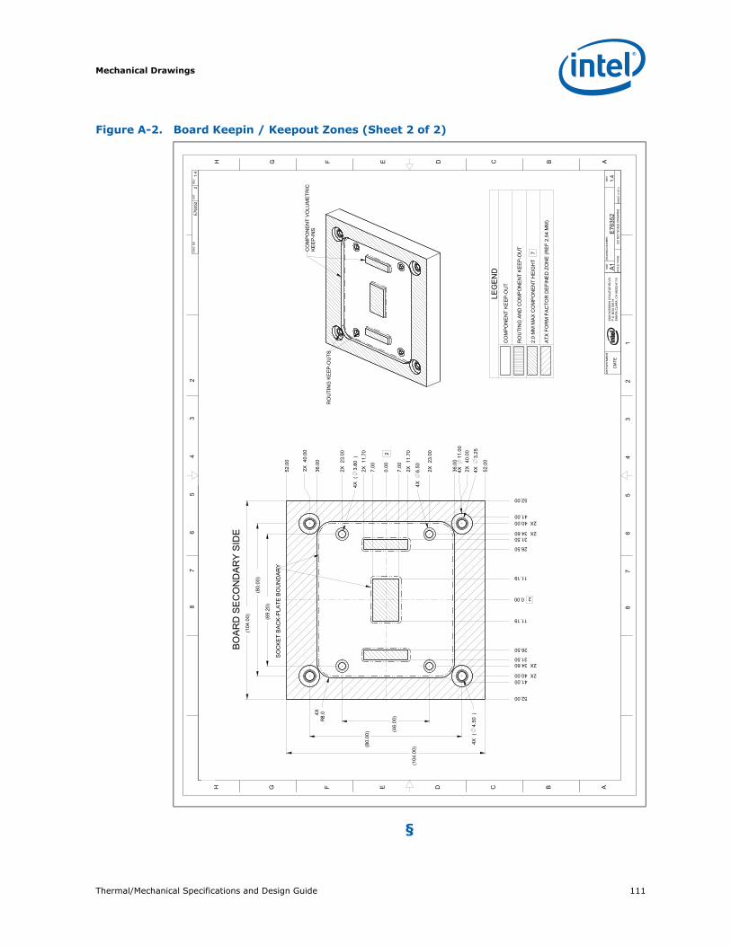
Thermal/Mechanical Specifications and Design Guide 111
Mechanical Drawings
§
Figure A-2. Board Keepin / Keepout Zones (Sheet 2 of 2)
H G F E D C B A
H G F E D C B A
8
7
6
5
4
3
2
8
7
6
5
4
3
2
1
R
52.0
0
0.00
2X 4
0.00
2X 2
3.00
36.0
0
2X 1
1.70
2X 1
1.70
2X 2
3.00
36.0
0
2X 4
0.00
52.0
0
52.00
0.00
41.002X 40.00
2X 34.60
2X 34.60
2X 40.00
52.00
41.00
4X
6.50
4X
3.25
31.50
26.50
11.19
11.19
26.50
31.507.
00
7.00
4X
11.0
0
4XR8
.0
(46.
00)
(69.
20)
4X (
)3.
80
(80.
00)
(80.
00)
(104
.00)
(104
.00)
4X (
)4.
50
TH
IS D
RA
WIN
G C
ON
TAIN
S IN
TEL
CO
RP
OR
ATI
ON
CO
NFI
DE
NTI
AL
INFO
RM
ATI
ON
. IT
IS D
ISC
LOS
ED
IN C
ON
FID
EN
CE
AN
D IT
S C
ON
TEN
TS M
AY
NO
T B
E D
ISC
LOS
ED
, RE
PR
OD
UC
ED
, DIS
PLA
YE
D O
R M
OD
IFIE
D, W
ITH
OU
T TH
E P
RIO
R W
RIT
TEN
CO
NS
EN
T O
F IN
TEL
CO
RP
OR
ATI
ON
.
E76
352
21.
4D
WG
. NO
SH
T.R
EV
DE
PA
RT
ME
NT
2200
MIS
SIO
N C
OLL
EG
E B
LVD
.P
.O. B
OX
581
19S
AN
TA C
LAR
A, C
A 9
5052
-811
9C
MTE
SIZ
E D
RA
WIN
G N
UM
BE
RR
EV
A1
E76
352
1.4
SC
ALE
: NO
NE
DO
NO
T SC
ALE
DR
AWIN
GS
HE
ET
2 O
F 2
BO
AR
D S
EC
ON
DA
RY
SID
E
2
2
SO
CK
ET
BA
CK
-PLA
TE B
OU
ND
AR
Y
CO
MP
ON
EN
T V
OLU
ME
TRIC
KE
EP
-INS
RO
UTI
NG
KE
EP
-OU
TS
LEG
EN
DC
OM
PO
NE
NT
KE
EP
-OU
T
RO
UTI
NG
AN
D C
OM
PO
NE
NT
KE
EP
-OU
T
2.0
MM
MA
X C
OM
PO
NE
NT
HE
IGH
T 7
ATX
FO
RM
FA
CTO
R D
EFI
NE
D Z
ON
E (R
EF
2.54
MM
)

Mechanical Drawings
112 Thermal/Mechanical Specifications and Design Guide
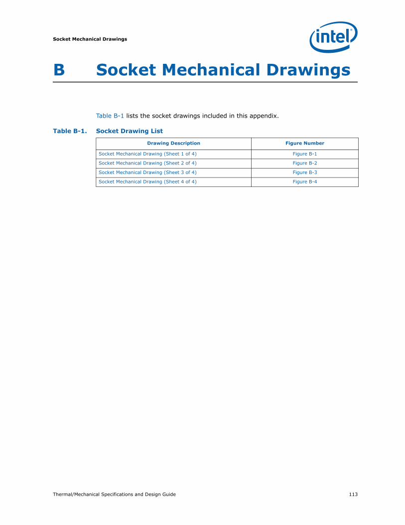
Thermal/Mechanical Specifications and Design Guide 113
Socket Mechanical Drawings
B Socket Mechanical Drawings
Table B-1 lists the socket drawings included in this appendix.
Table B-1. Socket Drawing List
Drawing Description Figure Number
Socket Mechanical Drawing (Sheet 1 of 4) Figure B-1
Socket Mechanical Drawing (Sheet 2 of 4) Figure B-2
Socket Mechanical Drawing (Sheet 3 of 4) Figure B-3
Socket Mechanical Drawing (Sheet 4 of 4) Figure B-4

Socket Mechanical Drawings
114 Thermal/Mechanical Specifications and Design Guide
Figure B-1. Socket Mechanical Drawing (Sheet 1 of 4)
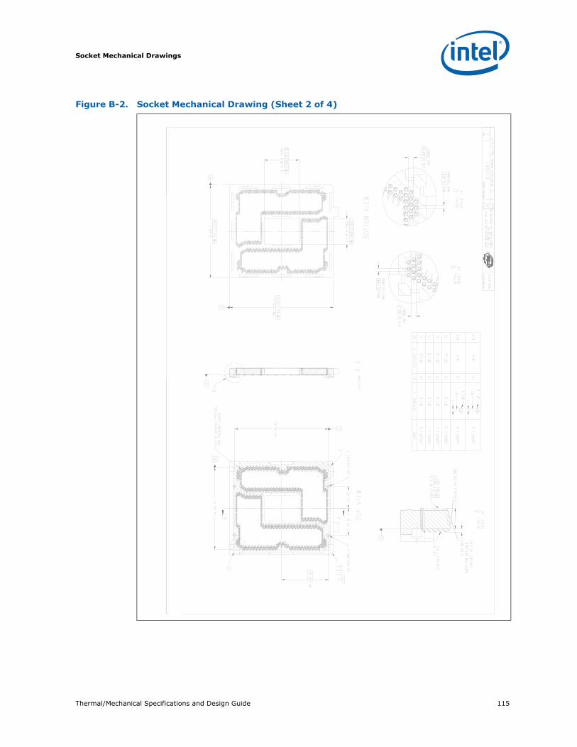
Thermal/Mechanical Specifications and Design Guide 115
Socket Mechanical Drawings
Figure B-2. Socket Mechanical Drawing (Sheet 2 of 4)
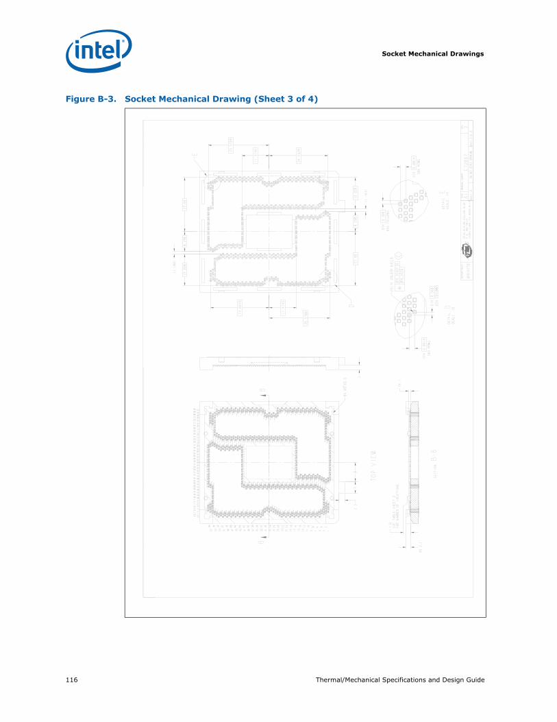
Socket Mechanical Drawings
116 Thermal/Mechanical Specifications and Design Guide
Figure B-3. Socket Mechanical Drawing (Sheet 3 of 4)
Thermal/Mechanical Specifications and Design Guide 117
Socket Mechanical Drawings
§
Figure B-4. Socket Mechanical Drawing (Sheet 4 of 4)

Socket Mechanical Drawings
118 Thermal/Mechanical Specifications and Design Guide
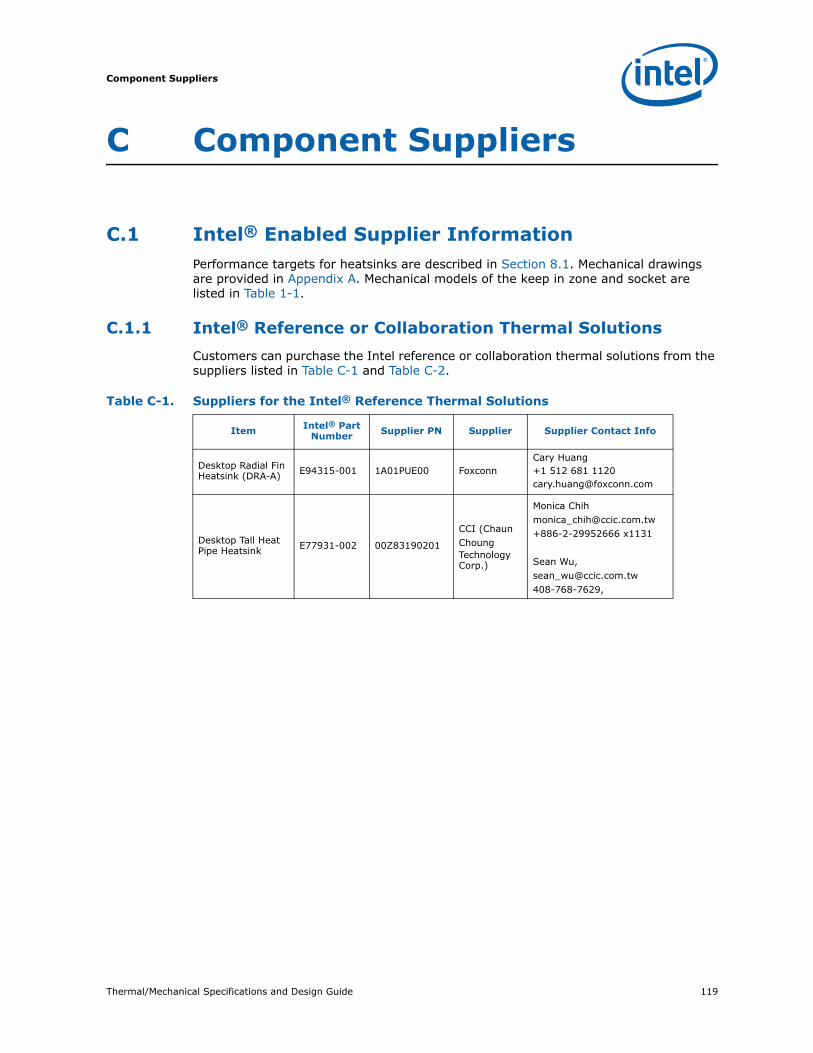
Thermal/Mechanical Specifications and Design Guide 119
Component Suppliers
C Component Suppliers
C.1 Intel® Enabled Supplier InformationPerformance targets for heatsinks are described in Section 8.1. Mechanical drawings are provided in Appendix A. Mechanical models of the keep in zone and socket are listed in Table 1-1.
C.1.1 Intel® Reference or Collaboration Thermal SolutionsCustomers can purchase the Intel reference or collaboration thermal solutions from the suppliers listed in Table C-1 and Table C-2.
Table C-1. Suppliers for the Intel® Reference Thermal Solutions
Item Intel® Part Number Supplier PN Supplier Supplier Contact Info
Desktop Radial Fin Heatsink (DRA-A) E94315-001 1A01PUE00 Foxconn
Cary Huang+1 512 681 [email protected]
Desktop Tall Heat Pipe Heatsink E77931-002 00Z83190201
CCI (Chaun ChoungTechnology Corp.)
Monica [email protected]+886-2-29952666 x1131
Sean Wu, [email protected],
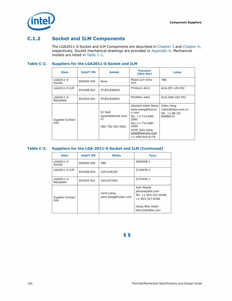
Component Suppliers
120 Thermal/Mechanical Specifications and Design Guide
C.1.2 Socket and ILM ComponentsThe LGA2011-0 Socket and ILM Components are described in Chapter 3 and Chapter 4, respectively. Socket mechanical drawings are provided in Appendix A. Mechanical models are listed in Table 1-1.
§ §
Table C-2. Suppliers for the LGA2011-0 Socket and ILM
Item Intel® PN Amtek Foxconn (Hon Hai) Lotes
LGA2011-0 Socket E64556-002 None PE201127-4351-
01HTBD
LGA2011-0 ILME91838-003 ITLE91838003
PT44L41-4411 ACA-ZIF-129-Y02
LGA2011-0 Backplate E91834-001 ITLE91834001 PT44P41-4401 DCA-HSK-182-T02
Supplier Contact Info
(86) 752 263 4562
(Socket) Katie [email protected]: +1-714-608-2085Fax:+1-714-680-2099(ILM) Julia Jiang [email protected] +1-408-919-6178
Cathy [email protected]: +1-86-20-84686519
Table C-3. Suppliers for the LGA-2011-0 Socket and ILM (Continued)
Item Intel® PN Molex Tyco
LGA2011-0 Socket E64556-002 TBD 2069458-1
LGA2011-0 ILME91838-003 1051428100
2134439-2
LGA2011-0 Backplate E91834-001 1051427000 2134440-1
Supplier Contact Info
Carol [email protected]
Josh [email protected]: +1-503-327-8348;+1-503-327-8346
(Asia) Billy [email protected]

Thermal/Mechanical Specifications and Design Guide 121
Package Mechanical Drawings
D Package Mechanical Drawings
Table D-1 lists the mechanical drawings included in this appendix.
Table D-1. Mechanical Drawing List
Drawing Description Figure Number
Processor Package Drawing (Sheet 1 of 2) Figure D-1
Processor Package Drawing (Sheet 2of 2) Figure D-2

Package Mechanical Drawings
122 Thermal/Mechanical Specifications and Design Guide
Figure D-1. Processor Package Drawing (Sheet 1 of 2)
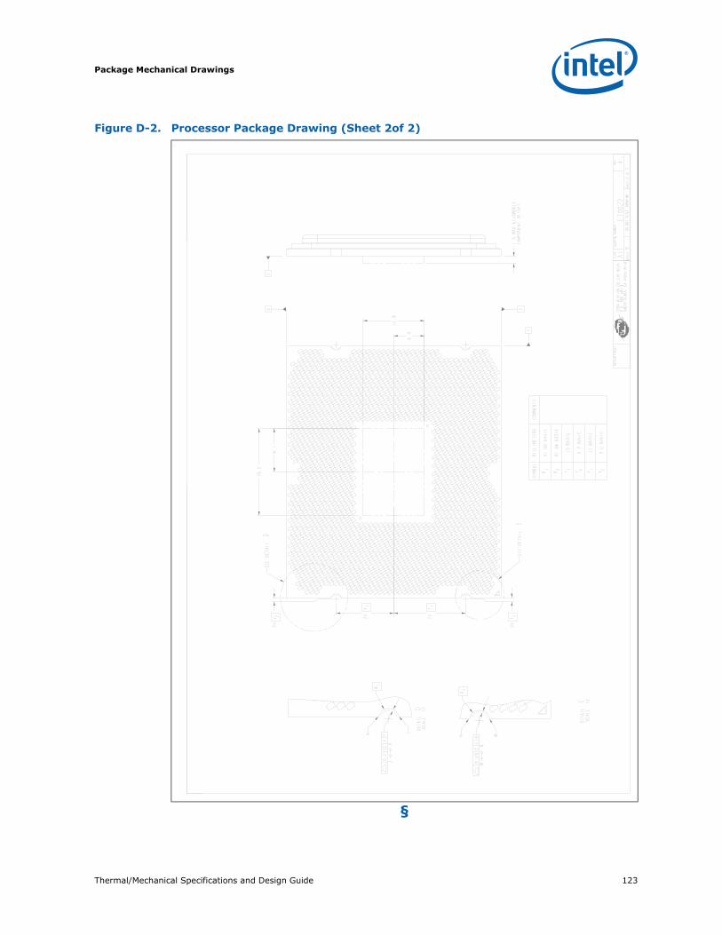
Thermal/Mechanical Specifications and Design Guide 123
Package Mechanical Drawings
§
Figure D-2. Processor Package Drawing (Sheet 2of 2).

Package Mechanical Drawings
124 Thermal/Mechanical Specifications and Design Guide