copyright by harish subbaraman 2009
TRANSCRIPT

Copyright
by
Harish Subbaraman
2009
The Dissertation Committee for Harish Subbaraman Certifies that this is the
approved version of the following dissertation:
Highly Dispersive Photonic Crystal Fibers for Optical True Time Delay
(TTD) Based X-Band Phased Array Antenna
Committee:
Ray T. Chen, Supervisor
Gary A. Hallock
Roger D. Bengtson
Seth R. Bank
Maggie Yihong Chen
Edward J. Powers
Highly Dispersive Photonic Crystal Fibers for Optical True Time Delay
(TTD) Based X-Band Phased Array Antenna
by
Harish Subbaraman, B.E.; M.S.E.
Dissertation
Presented to the Faculty of the Graduate School of
The University of Texas at Austin
in Partial Fulfillment
of the Requirements
for the Degree of
Doctor of Philosophy
The University of Texas at Austin
August, 2009

Dedicated to my Parents, Brother, Sister-in-Law and my Fiancée
v
Acknowledgements
I am greatly indebted to my supervisor Professor Ray T. Chen for providing me
with an excellent platform to learn things and for the invaluable advice and support
rendered during every aspect of my research work. This thesis also holds a great debt of
gratitude to Dr. Maggie Yihong Chen for closely monitoring my progress and providing me
with timely and important advice. I would also like to thank Dr. Gary A. Hallock, Dr.
Roger D. Bengtson, Dr. Seth R. Bank, and Dr. Edward J. Powers for their valuable time
and interest in this research. I also extend my special thanks to my colleagues and friends at
the Optical Interconnects Group for their help, assistance and advice especially Xiaonan
Chen, YongQiang Jiang, Lanlan Gu, Alan Wang, Xinyuan Dou, Beom-Suk Lee, Jian
Zhang, and Stephen Hsu. I also owe a great load of thanks to the staff at the
Microelectronics Research Center, especially Jean Toll, Joyce Kokes, Gerlinde Sehne and
Jackie Srnensky for their help with purchasing and procurement.
Finally, I want to thank my parents, brother and sister-in-law for always believing
in my abilities and for always showering their invaluable love and support. Most of all, I
want to thank my Fiancée Nirmala for her love, patience, support and encouragement
which made everything look doable and within reach.

vi
Highly Dispersive Photonic Crystal Fibers for Optical True Time Delay
(TTD) Based X-Band Phased Array Antenna
Publication No._____________
Harish Subbaraman, Ph. D
The University of Texas at Austin, 2009
Supervisor: Ray T. Chen
Phased array antenna (PAA) is a key component in many of the modern military
and commercial radar and communication systems requiring highly directional beams with
narrow beam widths. One of the advantages that this technology offers is a physical
movement-free beam steering. Radar and communication technologies also require the
PAA systems to be compact, light weight, demonstrate high bandwidth and
electromagnetic interference (EMI) free performance. Conventional electrical phase
shifters are inherently narrowband. This calls for technologies that have a larger bandwidth
and high immunity to electromagnetic interference. Optical true-time-delay (TTD)
technique is an emerging technology that is capable of providing these features along with
the ability to provide frequency independent beam steering. Photonic crystal fiber (PCF)
based optical TTD lines are capable of providing precise and continuous time delays
required for PAA systems.

vii
Photonic crystal fibers are a new class of optical fibers with a periodic arrangement
of air-holes around a core that can be designed to provide extraordinary optical
characteristics which are unrealizable using conventional optical fibers. In this dissertation,
highly dispersive photonic crystal fiber structures based on index-guidance and bandgap-
guidance were designed. Designs exhibiting dispersion coefficients as large as -
9500ps/nm/km and 4000ps/nm/km at 1550nm were presented. A TTD module utilizing a
fabricated highly dispersive PCF with a dispersion coefficient of -600ps/nm/km at 1550nm
was formed and characterized. The module consisted of 4 delay lines employing highly
dispersive PCFs connected with various lengths of non-zero dispersion shifted fibers. By
employing PCFs with enhanced dispersion coefficients, the TTD module size can be
proportionally reduced. A 4-element linear X-band PAA system using the PCF-TTD
module was formed and characterized to provide continuous time delays to steer radio-
frequency (RF) beams from -41 degrees to 46 degrees by tuning the wavelength from
1530nm to 1560nm.
Using the PCF-TTD based X-Band PAA system, single and simultaneous multiple
beam transmission and reception capabilities were demonstrated. Noise and distortion
performance characteristics of the entire PAA system were also evaluated and device
control parameters were optimized to provide maximum spurious-free-dynamic range. In
order to alleviate computational and weight requirements of practical large PAA systems, a
sparse array instead of a standard array needs to be used. X-Band sparse array systems
using PCF and dispersive fiber TTD technique were formed and RF beam steering was
demonstrated. As an important achievement during the research work, the design and
fabricated structure of a PCF currently reported to have the highest dispersion coefficient of
-5400ps/nm/km at 1549nm, along with its limitations was also presented. Finally, other

viii
interesting applications of highly dispersive PCFs in the areas of pulse compression and
soliton propagation were explored.

ix
Table of Contents
Page
Acknowledgements..............................................................................................................v
Abstract .............................................................................................................................. vi
List of Figures….............................................................................................................. xiv
List of Tables .................................................................................................................... xv
Chapter 1 Introduction ...................................................................................................1
1.1 Overview of Phased Array Antennas (PAA) .................................................1
1.1.1 Array Antenna.....................................................................................1
1.1.2 Phased Array Antenna ........................................................................4
1.1.2.1 Features of phased array antennas............................................6
1.1.2.2 Grating lobes ............................................................................8
1.1.3 Methods of phase control....................................................................9
1.2 Overview of true time delay (TTD) techniques ............................................11
1.3 Dispersive Fiber Prism Technique................................................................12
1.4 Highly dispersive Photonic Crystal Fiber (PCF) TTD based PAA ..............16
1.5 Objectives of the dissertation........................................................................17
1.6 Dissertation layout ........................................................................................18
1.7 References.....................................................................................................20
Chapter 2 Highly dispersive silica photonic crystal fibers.........................................24
2.1 Photonic crystal fibers....................................................................................24
2.1.1 Types of Photonic Crystal Fibers......................................................25
2.1.2 Maxwell’s equations and Bloch theorem..........................................27
2.2 Design of highly dispersive photonic crystal fibers.......................................29
2.2.1 Highly dispersive structures based on index-guiding PCF...............30
2.2.1.1 Working principle of a highly dispersive PCF based on a
dual concentric core design................................................31
2.2.1.2 Highly dispersive dual concentric-core PCF structure ......33
x
2.2.2 Highly dispersive structures based on air-guiding PCF.................43
2.2.3 Other highly dispersive PCF structures .........................................51
2.3 Fabrication of photonic crystal fibers ............................................................53
2.3.1 Stack and Draw Technique ............................................................53
2.3.2 Fabrication difficulties ...................................................................54
2.4 Summary........................................................................................................57
2.5 References......................................................................................................57
Chapter 3 Photonic crystal fibers based true-time delay modules for X-band phased
array antennas ............................................................................................61
3.1 Practical design of a highly dispersive photonic crystal fiber ......................61
3.2 Experimental characterization of true-time-delay (TTD) modules ..............65
3.2.1 Time delay interval measurement..................................................67
3.2.2 Phase-frequency curve measurement.............................................69
3.3 Summary.......................................................................................................73
3.4 References.....................................................................................................74
Chapter 4 1x4 X-band phased array antenna subsystem for single beam
transmission/reception................................................................................75
4.1 Demonstration of single RF beam transmission of PCF-TTD based X-band
PAA...............................................................................................................75
4.1.1 Principle of single RF beam transmission .....................................76
4.1.2 Experimental setup.........................................................................78
4.1.3 Results and discussion ...................................................................83
4.2 Demonstration of single RF beam reception of PCF-TTD based X-band
PAA...............................................................................................................86
4.2.1 Principle of single RF beam reception...........................................86
4.2.2 Experimental setup.........................................................................87
4.2.3 Results and discussion ...................................................................89
4.3 Summary.......................................................................................................91
4.4 References.....................................................................................................91

xi
Chapter 5 Simultaneous multiple-beam transmission and reception of a PCF
TTD-based X-band phased array antenna ...............................................94
5.1 Principle of simultaneous multiple RF beam transmission...........................94
5.2 Demonstration of simultaneous multiple beam transmission of a PCF-TTD
based X-band PAA .......................................................................................97
5.2.1 Experimental setup.........................................................................97
5.2.2 Results and discussion ...................................................................98
5.3 Principle of simultaneous multiple RF beam reception..............................100
5.4 Demonstration of simultaneous multiple beam reception of a PCF-TTD
based X-band PAA .....................................................................................102
5.4.1 Experimental setup.......................................................................102
5.4.2 Results and discussion .................................................................107
5.5 Summary.....................................................................................................109
5.6 References...................................................................................................109
Chapter 6 Characterization and RF performance evaluation of PCF-TTD analog
subsystem...................................................................................................111
6.1 Noise in analog links...................................................................................111
6.1.1 Noise sources ...............................................................................112
6.1.2 Noise figure (NF) measurement...................................................115
6.2 Distortion in analog links............................................................................118
6.2.1 Harmonic distortion .....................................................................119
6.2.2 Intermodulation distortion ...........................................................120
6.3 Sources of distortion ...................................................................................121
6.4 Harmonic distortion measurement..............................................................122
6.5 Intermodulation distortion measurement ....................................................124
6.5.1 Spurious-Free Dynamic Range (SFDR) ......................................124
6.5.2 SFDR measurement .....................................................................125
6.6 Improving SFDR using high power Erbium-doped fiber amplifier............129
6.6.1 Principle of operation...................................................................129

xii
6.6.2 Experimental results.....................................................................130
6.7 Summary......................................................................................................133
6.8 References....................................................................................................133
Chapter 7 X-band Sparse Array Antenna Demonstration .......................................135
7.1 Why do we require sparse array?................................................................135
7.1.1 Simulation results.........................................................................136
7.2 Sparse Array Antenna.................................................................................139
7.3 Highly dispersive PCF based sparse array..................................................141
7.4 Highly dispersive fiber – based sparse array antenna.................................144
7.4.1 Time delay measurement .............................................................145
7.4.2 Experimental setup.......................................................................146
7.4.3 Far-field radiation pattern ............................................................148
7.5 Summary......................................................................................................150
7.6 References....................................................................................................151
Chapter 8 Other important achievements.................................................................152
8.1 PCF with highest dispersion coefficient .....................................................152
8.1.1 Structural design of the PCF........................................................152
8.1.2 Dispersion coefficient ..................................................................156
8.1.3 Limitations of the PCF.................................................................158
8.2 Pulse Compression......................................................................................159
8.2.1 Principle of operation...................................................................159
8.2.2 Experimental setup and results ....................................................161
8.3 Summary......................................................................................................164
8.4 References....................................................................................................164
Chapter 9 Recommendations for Future work.........................................................166
9.1 2-D continuously tunable photonic crystal fiber true-time delay modules for
standard and sparse phased array antenna systems..................................166
9.2 Other applications of highly dispersive PCF ..............................................167
9.2.1 Soliton propagation......................................................................167

xiii
9.3 Summary......................................................................................................169
Chapter 10 Summary ....................................................................................................171
Appendix Publications of Harish Subbaraman...............................................................174
Bibliography ....................................................................................................................176
Vita...................................................................................................................................190

xiv
List of Tables
Table 3.1 Measured time delay (in ps) from four true-time-delay lines........................... 71 Table 7.1 Measured dispersion coefficient of the DCF..................................................146
xv
List of Figures
Fig. 1.1 Schematic diagram of a linear antenna array......................................................... 2 Fig. 1.2 Schematic diagram of a Phased-Array Antenna (PAA) ........................................ 5 Fig. 1.3 Radiation pattern dependence on single element pattern ...................................... 7 Fig. 1.4 Radiation pattern of an 8 element PAA with grating lobes................................... 9 Fig. 1.5 (a) Beam-Squint effect of a phased array antenna controlled by electrical phase shifters (b) Nature of a phased array antenna controlled by true-time-delay network ..... 10 Fig. 1.6 Fiber-Optic Prism true-time-delay feed network [6] ...........................................13 Fig. 1.7 Schematic of the Highly Dispersive PCF-TTD based PAA. MZM: Mach-Zehnder modulator; EDFA: Erbium-doped fiber amplifier, TTD: true time delay, LNA: low noise amplifier. (PCF is represented with red dots and non-zero dispersion shifted fibers is represented with blue dots) ................................................................................. 17 Fig. 2.1 SEM cross-sections of (a) Index-guiding PCF [1] (b) Photonic bandgap guiding PCF [13]............................................................................................................................ 26 Fig. 2.2 Schematic cross section of the designed dual concentric core PCF.................... 34 Fig. 2.3 Mode profile of the dual concentric-core PCF at (a) λ<λp (b) λ≈λp and (c) λ>λp
........................................................................................................................................... 35 Fig. 2.4 Variation of λddn / with respect to the period (Λ) for the inner core (filled squares) and outer core (empty squares)........................................................................... 36 Fig. 2.5 Calculation result (stars) and its curve fit (circles) for the relationship between T and Period (Λ)................................................................................................................... 37 Fig. 2.6 Effect of coupling on the effective refractive index ............................................ 39 Fig. 2.7 Relationship between the dispersion value D and wavelength and comparison of Plane Wave Expansion (filled squares) and Coupled-Mode Theory (empty circles) results........................................................................................................................................... 40 Fig. 2.8 Variation of the dispersion value and the shift observed due to (a) variation in the pitch, (b) variation of d1, (c) variation of d2, and (d) variation of d3, while keeping all the other parameters as in the given design in each case........................................................ 42 Fig. 2.9 Variation of dispersion with number of air hole rings between the inner and the outer core .......................................................................................................................... 43 Fig. 2.10 Schematic cross section of the designed photonic bandgap fiber ..................... 45 Fig. 2.11 (a) Frequency versus propagation constant relation for the cladding showing forbidden regions (gap) within which no solution to Maxwell’s equations exists (b) The gap edges are plotted showing the light line (frequency = propagation constant) ........... 46 Fig. 2.12 Computed transverse mode profiles of the designed highly dispersive bandgap fiber showing (a) Fundamental mode (b) and (c) higher order modes ............................. 48 Fig. 2.13 Calculated effective refractive index of the fundamental guided mode (neff) as a function of wavelength ..................................................................................................... 48 Fig. 2.14 Dispersion curve of the simulated highly dispersive photonic bandgap fiber... 49 Fig. 2.15 Effect of change of period (P) on the dispersion curve for 3.85µm (black curve), 3.86µm (red curve), and 3.87µm (green curve) ................................................................ 50 Fig. 2.16 Dispersion coefficient for PCF structure with a small air-hole at the center (cross section of the designed fiber is also shown)........................................................... 51 Fig. 2.17 Dispersion coefficient for PCF structure with doping-induced refractive index change of the cores............................................................................................................ 52

xvi
Fig. 2.18 Schematic of stack and draw method for fabricating photonic crystal fibers [36]........................................................................................................................................... 53 Fig. 2.19 Dmax-FWHM product plotted as a function of PCF parameters. The solid lines are only to aid the human eye. The data points are marked with solid squares................ 56 Fig 3.1(a) Scanning electron microscope (SEM) images of the fabricated high dispersion PCF [1-2] (b) Schematic cross section of the PCF ........................................................... 62 Fig. 3.2 Simulated transverse mode profiles of the highly dispersive photonic crystal fiber when (a) pλλ < (b) pλλ > and (c) pλλ ≈ .................................................................... 63
Fig. 3.3 Simulated dispersion coefficient of the designed highly dispersive photonic crystal fiber ....................................................................................................................... 64 Fig. 3.4 Schematic representation of connection between NZ-DSF and PCF using UHNA fiber (only connections at one end of PCF are shown)..................................................... 66 Fig. 3.5 Measured dispersion coefficient of the fabricated highly dispersive photonic crystal fiber ....................................................................................................................... 67 Fig. 3.6 Schematic of the time delay interval measurement setup using femtosecond laser source ................................................................................................................................ 68 Fig. 3.7 Time delayed pulse traces of 4 TTD lines measured on the digital communication analyzer ............................................................................................................................. 69 Fig. 3.8 Schematic of Phase versus Frequency measurement setup................................. 70 Fig. 3.9 Phase versus Frequency plots for (a) TTD line consisting of 3.5m PCF and 7.0m NZ-DSF, (b) TTD line consisting of 7.0m PCF and 3.5m NZ-DSF, (c) TTD line consisting of 10.5m PCF and 0m NZ-DSF....................................................................... 71 Fig. 3.10 Calculated steering angle of X-band PAA with antenna element spacing
cmd 3.1= .......................................................................................................................... 72 Fig. 4.1 Schematic of the Highly Dispersive PCF-TTD based PAA setup for single RF beam transmission (PCF is represented with red dots and non-zero dispersion shifted fibers is represented with blue dots) ................................................................................. 76 Fig. 4.2 Experimental setup of the PAA in transmitting mode (a) Overall setup along with an expanded view of the antenna array is shown. (b) The four TTD lines are shown. The inset shows the composition of each line. (c) The receiving horn antenna and the microwave spectrum analyzer are shown ......................................................................... 81 Fig. 4.3 Measured normalized element pattern of the patch antenna at 9GHz................. 82 Fig. 4.4 Simulated and measured far field patterns for (a) RF signal with frequency = 8.4GHz at a wavelength of 1547.72nm. (b) RF signal with frequency = 12GHz at a wavelength of 1552.52nm................................................................................................. 84 Fig. 4.5 Beam squint-free demonstration of the PCF-TTD based phased array antenna system ............................................................................................................................... 85 Fig. 4.6 Schematic of the Highly Dispersive PCF-TTD based PAA system for single RF beam reception. MZM: Mach-Zehnder modulator; TTD: true time delay, LNA: low noise amplifier, MSA: Microwave spectrum analyzer (PCF is represented with red dots and non-zero dispersion shifted fibers is represented with blue dots).....................................88 Fig. 4.7 Measured received power versus wavelength for (a) 8.4GHz RF signal impinging on the antenna array from -7.40 (b) 12GHz RF signal impinging on the antenna array from -21.20 ........................................................................................................................ 90
xvii
Fig. 5.1 Schematic setup for simultaneous transmission of multiple beams, EOM: electro-optic modulator, EDFA: Erbium doped fiber amplifier, TTD: true-time-delay. The cross sectional schematic view of the PCF is also shown ................................................ 95 Fig. 5.2 Experimental setup for simultaneous dual RF beam steering, EDFA: Erbium doped fiber amplifier, TTD: true-time-delay, LNA: low noise amplifier, TDL: tunable delay line........................................................................................................................... 98 Fig. 5.3 Simulated and Measured Far Field Patterns of two RF signals with frequencies 8.4GHz and 12GHz steered simultaneously to angles of 7.4 and 21.2 degrees respectively........................................................................................................................................... 99 Fig. 5.4 Structure of the receiving mode with multiple incoming beams, WDM: wavelength division multiplexer, LNA: low noise amplifier, EOM: electro-optic modulator, TTD: true-time-delay, DEMUX: demultiplexer ........................................... 101 Fig.5.5 Schematic of simultaneous dual beam operation setup and photograph of actual (a) RF reception and electro-optical conversion setup (b) True-Time-Delay lines and signal processing setup; the output from the modulators in (a) are connected to the inputs of EDFAs in (b). (The RF sources and the transmitting horn antennas of the setup are not shown in the figure) ........................................................................................................ 105 Fig. 5.6 Signal power measured at the photodetector vs. wavelength. The signal power peaks appear at 1547.72nm for 8.4GHz and 12GHz signals placed at -7.4 degrees and at 1552.52nm for 8.4GHz and 12GHz signals placed at -21.2 degrees.............................. 106 Fig. 6.1 Schematic of the setup used for noise figure measurement............................... 116 Fig. 6.2 Noise Figure versus Modulator bias measurement for PCF-TTD system at 20mW optical input power ......................................................................................................... 118 Fig 6.3 Spectrum plot of output RF signals from a component having a nonlinear transfer function ........................................................................................................................... 119 Fig. 6.4 Measured fundamental (black curve), second harmonic (red curve) and third harmonic (green) powers as a function of modulator bias.............................................. 123 Fig. 6.5 Experimental setup for spurious-free dynamic range measurement. EDFA: Erbium-Doped Fiber Amplifier; MZM: Mach-Zehnder Modulator; TTD: True-Time-Delay; MSA: Microwave Spectrum Analyzer; LNA: Low-Noise Amplifier................. 126 Fig. 6.6 Fundamental and IMD-3 output powers as observed on a microwave spectrum analyzer ........................................................................................................................... 127 Fig. 6.7 Fundamental (red squares) and IMD-3 (blue circles) RF output powers as a function of input RF power. Optical input power of 20mW and modulator bias angle of 90 degrees are used. Extrapolated straight line fits to the data points are also shown. The extrapolated lines intersect at a point whose corresponding RF input power gives IIP3128 Fig. 6.8 Measured link noise figure as a function of modulator bias angle for different optical input powers........................................................................................................ 130 Fig. 6.9 Fundamental (red squares) and IMD-3 (blue circles) RF output powers as a function of input RF power. Optical input power of 200mW and modulator bias angle of 153 degrees are used. Extrapolated straight line fits to the data points are also shown. The extrapolated lines intersect at a point whose corresponding RF input power gives IIP3132 Fig. 7.1 Array factor simulation of a 100 element standard array with inter-element
spacing 2
λ=d at 12.5GHz ............................................................................................. 136
xviii
Fig. 7.2 Array factor simulation of an 8 element sparse array with inter-element spacing
2*14
λ=d at 12.5GHz ................................................................................................... 137
Fig. 7.3 X-band sparse array antenna consisting of three periodically spaced horn antennas spaced 0.168m apart, equivalent to a 29-element standard array (precision rotation stage is also shown)........................................................................................... 139 Fig. 7.4 Measured S11 parameter of three antenna elements........................................... 140 Fig. 7.5 Measured normalized patterns of 3 antenna elements at a frequency of (a) 9GHz and (b) 10GHz................................................................................................................. 141 Fig. 7.6 Simulated and Measured far-field radiation patterns of the sparse array antenna at an optical wavelength of (a) 1559.9nm corresponding to +3degree beam steering and (b) 1529.9nm corresponding to -3degree beam steering (blue arrows indicate the desired beam, dashed red arrows at 0degree indicate the beam steering angle at center wavelength of 1545nm)...................................................................................................................... 143 Fig. 7.7 Experimental setup for sparse array antenna demonstration, LNA: low-noise amplifier; MZM: Mach-Zehnder modulator; TTD: true-time-delay .............................. 147 Fig. 7.8 Simulated (dashed curve) and Measured (curve marked with data points) far-field radiation patterns of the sparse array antenna at an optical wavelength of 1558.65nm corresponding to +11degree beam steering of a 9GHz RF signal (blue arrow indicates the desired beam). Measured pattern at central wavelength of 1555nm is also shown as a dashed red curve with peak at 0 degrees indicated by a red arrow................................. 148 Fig. 7.9 Simulated (dashed smooth curves) and Measured (curves marked with data points) far-field radiation patterns of the sparse array antenna at an optical wavelength of 1550nm corresponding to -15degree beam steering of a 9GHz (red curves) and a 10GHz RF signal (green curves) ................................................................................................. 150 Fig. 8.1 Cross section of the designed photonic crystal fiber. The periodicity of the structure is given by Λ. A high index central core (d1) is surrounded by an inner cladding (d2) consisting of air holes. Outer core (d3) has slightly lower refractive index compared to the central core. All other air holes (d4) form the outer cladding region.................... 153 Fig. 8.2 Scanning electron microscope (SEM) picture of the cross section of the fabricated highly dispersive PCF (Enlarged views of the highlighted sections are also shown)............................................................................................................................. 154 Fig. 8.3 Simulated dispersion coefficient for the designed high dispersion PCF with selective injecting into the inner core (red curve) and with random injection (black curve)......................................................................................................................................... 155 Fig. 8.4 System setup to measure dispersion value of PCF using phase-shift method... 156 Fig. 8.5 Simulated dispersion curves for selective injection (dashed red curve), random injection (dashed green curve) and measured dispersion curve (green curve with marked circles) of the PCF .......................................................................................................... 158 Fig. 8.6 Experimental setup for demonstrating pulse compression................................ 162 Fig. 8.7 Pulse compression demonstration with (a) Input pulse launched into the PCF (FWHM = 2898fs, pulse width = 1.848ps) (b) Output pulse as measured on the autocorrelator (FWHM = 630fs, pulse width = 401.94fs) .............................................. 163 Fig. 9.1 Schematic setup of TTD based 2-D Phased Array Antenna, MZM: Mach-Zehnder modulator; TTD: true-time-delay; WC: wavelength convertor; PD: photodetector; LNA: low-noise amplifier....................................................................... 166

xix
Fig. 9.2 Measured pulse traces of soliton from the PCF at different pump current levels......................................................................................................................................... 169

1
Chapter 1 Introduction
1.1 Overview of Phased Array Antennas (PAA)
An antenna is a device that can transmit and receive electromagnetic wave
energy. It forms the basic component for electronic systems based on free space
propagation such as satellite communication, mobile communication, radar, air traffic
control etc. Antennas can be classified based on bandwidth into narrow band antennas
and broad band antennas and they can also be classified based on their radiation pattern
into directional antennas and isotropic antennas. It is possible to create a highly
directional antenna by arranging individual antenna elements in linear, circular,
rectangular etc patterns. Directional antennas have a very high signal-to-noise (S/N) ratio
compared to individual radiating elements. A phased array antenna (PAA) is a special
kind of an array antenna wherein the beam pointing direction can be changed without
mechanically moving the antenna head. The principle behind the working of a PAA can
be understood by first understanding the working of an antenna array. Therefore, this
section begins with the development of theory for an antenna array, followed by an
extension of the theory to phased array antennas.
1.1.1 ARRAY ANTENNA
In order to understand the working principle of a phased array antenna (PAA), a
simple linear antenna array is explained first, followed by development of theory for
PAA in the next section. A linear array consisting of K identical antenna elements with a
separation between elements given by d is shown in Fig. 1.1. It is mathematically
convenient to assume the antenna array to be working in the receiving mode. This is not a

2
restriction on the antenna, because by the virtue of reciprocity theorem, the transmission
characteristics are similar to the receiving characteristics [1]. The incoming
electromagnetic beam from an angle theta (θ ) impinges on the array in such a way that
the wavefront first reaches element K, and due to the additional distance traveled by the
wavefront to reach every element, a different phase is received by each element.
Fig. 1.1 Schematic diagram of a linear antenna array
The phase of all other elements (iφ ) with respect to element K can be obtained by
multiplying the path length difference with the free-space wave number 0k [1]
)sin()(0 θφ diKki −= (1.1)
where 0
0
2
λπ=k and 0λ is the free-space wavelength and i = 1, 2, 3…K

3
If ia is the amplitude received by each antenna element and )(θelS is the complex
radiation pattern of each antenna element, then the complex signal received by each
element can be written as:
)sin()(0)()( θθθ diKjkieli eaSS −= (1.2)
Without introducing any additional phase shifts, the signals from all the elements
can be combined and the overall received signal )(θS can be written as:
∑=
−=K
i
diKjkiel eaSS
1
)sin()(0)()( θθθ (1.3)
Here, )(θelS is assumed to be the same for all the elements. This is a reasonable
assumption because, in a practical antenna array, the antenna elements are very identical.
Let us also assume that the amplitudes received by the individual antenna elements are
equal, i.e. ai = 1.
∑=
−=K
i
diKjkel eSS
1
)sin()(0)()( θθθ (1.4)
and, )()()( θθθ ael SSS = (1.5)
where ∑=
−=K
i
diKjka eS
1
)sin()(0)( θθ is called the array factor.
From equation (1.4) we see that )(θS is maximum for θ = 0 degrees. This is
called the broadside of the array. The above expressions are derived assuming far-field
approximations. A far field is the region wherein the angular distribution of the radiating

4
fields is independent of the distance to the antenna. The required distance R where one
can safely use far-field approximations is given by [1]
RF
DR
λ
22= (1.6)
where, D is the largest dimension of the array and RFλ is the radio frequency (RF) signal
wavelength.
1.1.2 PHASED ARRAY ANTENNA (PAA)
Using the results from section 1.1.1 on array antennas, let us examine what would
happen if we intentionally added additional phase terms ( iψ ) to each antenna element as
shown in Fig. 1.2. The array factor from the previous section changes and incorporates
this additional phase term to become:
∑=
+−=K
i
diKkja
ieS1
)sin()(0)( ψθθ (1.7)
Depending on the value of iψ , the following three cases are encountered:
Case 1:
If iψ = 0, then equation (1.7) becomes:
∑=
−=K
i
diKkja eS
1
)sin()(0)( θθ (1.7 a)
This is just the case of an array antenna wherein the maximum occurs at θ = 0 degrees.
This is the broadside of the array.
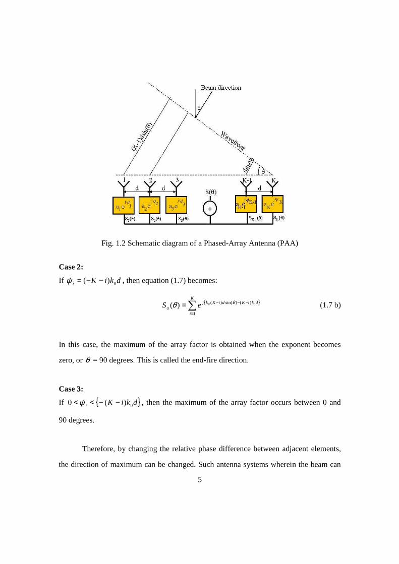
5
Fig. 1.2 Schematic diagram of a Phased-Array Antenna (PAA)
Case 2:
If dkiKi 0)( −−=ψ , then equation (1.7) becomes:
∑=
−−−=K
i
dkiKdiKkja eS
1
)()sin()( 00)( θθ (1.7 b)
In this case, the maximum of the array factor is obtained when the exponent becomes
zero, or θ = 90 degrees. This is called the end-fire direction.
Case 3:
If dkiKi 0)(0 −−<<ψ , then the maximum of the array factor occurs between 0 and
90 degrees.
Therefore, by changing the relative phase difference between adjacent elements,
the direction of maximum can be changed. Such antenna systems wherein the beam can
6
be steered by changing the phase are called Scanned-Beam Array Antenna or Phase-
Steered Antenna or Phased-Array Antenna (PAA)
Phased Array Antennas are getting more and more important in present-day
communications. One primary advantage that such PAA systems offer over other antenna
systems is that in order to transmit/receive an electromagnetic field to/from any direction,
mechanical movement of the antenna body is not necessary. Also, these antennas have
low visibility which means that such antenna arrays cannot be detected as there are no
moving parts. Quick steering of beams is possible either by using electrically or optically
controlled networks. These systems are also small in terms of size and weight.
Furthermore, they can be used for multi-mode operation, having simultaneous multiple
steering beams that cover a large area [2, 3]. Due to so many advantages over a single
antenna, phased array antennas are widely used in both civilian operations, such as air
traffic control and mobile communication, satellite communications, and in the military
operations, such as radar, missile guidance, trajectory determination, and satellite
communications etc.
1.1.2.1 Features of phased array antennas
Till this point, emphasis has been on the characteristics of the array factor and
how the phase fed to the individual antenna elements changes the beam pointing direction
or the steering angle. Although the beam pointing direction strictly depends on the
antenna factor, the overall radiation pattern depends both on the element radiation pattern
)(θelS and the array factor )(θaS according to equation (1.5).
If we write down the complex radiation pattern in the logarithmic form, then
7
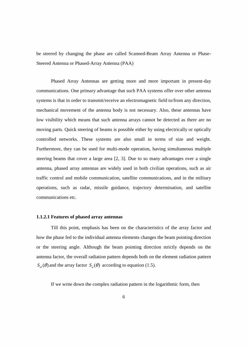
)(log20)(log20)( θθθ ael SSdBS += (1.8)
Fig. 1.3 shows the radiation pattern of an 8 element linear array with inter-
element spacing = 1.25cm working at 12GHz and with phase information provided such
that the maximum occurs at 20 degrees. The voltage radiation pattern of the individual
elements is assumed to be of the form )cos()( θθ =elS . The dashed red pattern, the dotted
blue pattern and the solid green pattern correspond to element, array factor and overall
radiation patterns respectively.
-60
-50
-40
-30
-20
-10
0-60 -40 -20 0 20 40 60
Angle (Degrees)
Norm
aliz
ed P
ow
er (dB
)
Single element pattern
Array Factor
Radiation Pattern
Fig. 1.3 Radiation pattern dependence on single element pattern
The part of the radiation pattern with the highest power is called the main beam.
All other lobes are called side lobes. It can be seen from the figure that the element
pattern only acts as a filter at larger angles and the peak radiation direction is still
determined by the array factor. Due to this filtering effect, there is a small error in the

8
beam pointing direction at larger angles and is slightly less than that given by the array
factor.
1.1.2.2 Grating Lobes
We can rewrite equation (1.7) by inserting )sin()( 00 θψ kiKi −−= for a general
value of 0θ lying in between -90 and 90 degrees as
∑=
−−=K
i
diKjka eS
1
)sin()sin()( 00)( θθθ (1.9)
From the above equation, we see that whenever πθθ ndk 2)sin()sin( 00 =− ,
where n is an integer, the array factor repeats itself, i.e. the lobes reoccurs in the angular
space as long as πθθλπ
nd 2)sin()sin(2
00
=− or )sin()sin(
1
00 θθλ −=d
. The lobe at n=0
is called the main lobe and all other lobes are called grating lobes. For 00 9090 ≤≤− θ ,
)sin(θ value lies between -1 and 1. In order to avoid grating lobes, the pitch of the
antenna array must be chosen in such a manner that
max0 )sin(1
1
θλ +<d
(1.10)
Therefore, for a maximum scan angle of 090± , the grating lobes can be avoided
as long as
2
1
0
≤λd
(1.11)
The effect of antenna element spacing on the array factor is shown in Fig. 1.4.
Similar parameters as chosen for Fig. 1.3 are chosen, but the spacing between elements is

9
set as 5cm. It can be seen from the figure that the grating lobes occur for a 12GHz signal
at -41.1 degrees, -9 degrees, and 57.3 degrees with the main lobe occurring at 20 degrees.
-80
-70
-60
-50
-40
-30
-20
-10
0-60 -40 -20 0 20 40 60
Angle (Degrees)
No
rmal
ized
Po
wer
(d
B)
Fig. 1.4 Radiation pattern of an 8 element PAA with grating lobes
1.1.3 METHODS OF PHASE CONTROL
Since controlling phase in PAA systems is of paramount importance, it is
worthwhile to introduce the techniques of phase control in this section. Primarily, there
are two ways to control the phase of individual elements in the array
1. Using Electrical Phase Shifters
2. Using True Time Delay (TTD)
Conventional electrical phase shifters or phase trimmers are inherently narrow
band and they add a constant phase in the frequency range of interest. Therefore, the
radiation peak angle changes with frequency according to the relation:

10
ωωθθ ∆−=∆ )tan( 00 (1.12)
Therefore, there is a change in the beam pointing direction due to a change in the
operating frequency. This effect is called beam squint and is highly undesirable in various
military and civilian applications. The beam squint effect is illustrated in Fig. 1.5(a). The
radiation pattern simulation is performed for a 16 element linear PAA with separation
between adjacent elements equal to 1.5cm and the beam pointing direction is chosen as
30 degrees. It can be seen from the figure that as the operating frequency is changed from
8GHz to 12GHz, the beam pointing direction changes from 38.6 degrees to 24.6 degrees.
Therefore, an extremely narrow range of frequencies around the center frequency can be
used in the system operation.
Fig. 1.5 (a) Beam-Squint effect of a phased array antenna controlled by electrical phase shifters (b) Nature of a phased array antenna controlled by true-time-delay
network
(b) (a)
11
Modern day PAA applications demand a broad bandwidth and a squint-free
operation with characteristics as shown in Fig. 1.5(b). Irrespective of the frequency used,
all the main lobes point to 30 degrees. Therefore, instead of proving a constant phase at
all frequencies, the system should be able to provide phase that linearly changes with
frequency. Such systems are called true-time-delay (TTD) systems wherein the time delay
is independent of the frequency of operation.
1.2 Overview of true-time-delay (TTD) techniques
In this section, an overview of the various true-time-delay techniques will be
covered. The TTD techniques can be further classified into electrical-TTD and optical-
TTD. The electrical TTD technique is a very mature technique. Electrical TTD mainly
includes the binary path selection TTD technique and the length tunable waveguide TTD
technique [4]. The binary path selection technique is highly efficient for large phased
array antenna configurations. The length tunable waveguide TTD technique suffers from
inherent disadvantages of error in time delay with increasing frequency of operation and
a very small maximum time delay value leads to a small angular range in beam steering.
Nonetheless, it is relatively easier to configure the electrical TTDs compared to optical
TTD networks. One major disadvantage that the electrical TTD suffers from is that the
modules are prone to electromagnetic interference (EMI). Although optical TTD is not as
easily configurable as its electrical counterpart, there has been a growing interest in this
technique due to features such as large time delay with squint-free beam steering, wide
bandwidth, reduced system weight and size, and low electromagnetic interference (EMI)
when compared with electrical TTD techniques [5-9]. However, most of the optical TTD
techniques require a large number of electro-optical elements such as lasers, optical
modulators, photodiodes, etc resulting in a complex system design that may also suffer

12
from large power losses and may require specialized components. Sometimes, it also
becomes cumbersome to extend these systems to 2-D arrays.
Optical TTD techniques can be further divided into discrete and continuously
tunable techniques. Examples of discrete optical TTD techniques are bulk optical TTD
technique [10-14], optical non-dispersive fiber TTD technique [15], wavelength-division-
multiplexer TTD technique [16-21], holographic-grating based TTD technique [8, 22],
wavelength-selective waveguide TTD technique [23], acoustic-optic TTD technique [24-
27]. Examples of continuously tunable optical TTD techniques are optical dispersion
based TTD technique [7], dispersive fiber prism based TTD technique [6, 28, 29, 30],
chirped fiber grating based TTD technique [31, 32], and holographic-grating based TTD
technique [33-35]. The dispersive fiber prism TTD technique involves using conventional
dispersion compensating fiber which have a relatively small dispersion coefficient, D = -
100ps/nm/km, and therefore long fiber lengths are required in the TTD module to achieve
the required time delay. Therefore, by increasing the dispersion coefficient, the module
size can be decreased proportionally.
1.3 Dispersive Fiber Prism Technique
The highly dispersive photonic crystal fiber true-time-delay (TTD) network
presented in this work is based on a method called the dispersive fiber prism technique
[6, 28, 29, 30]. This technique was first proposed and demonstrated by Esman et al in the
year 1992. The schematic of the setup used by Esman et al is shown in Fig. 1.6 [6].

13
Fig. 1.6 Fiber-Optic Prism true-time-delay feed network [6]
A microwave input signal is modulated onto an optical carrier generated by a
tunable laser source using an electro-optic modulator (EOM). This modulated optical
carrier is split to N channels via a 1-to-N splitter. These N output channels feed a
dispersive fiber prism true-time-delay network consisting of a series of N delay lines.
Each delay line consists of a highly dispersive fiber (HDF) connected to a non-dispersive
fiber (NDF) with an overall length approximately equal between adjacent lines. After
passing through the dispersive fiber prism, each optical signal is converted to an electrical
signal at the photodetector (PD) and is fed to each element in the antenna array. The
lengths of the dispersive and the non-dispersive fibers in each line are carefully chosen
such that at a central optical wavelength0λ , the delay through all the lines are equal, i.e.
all the signal arrive in phase at the output. Since there is no phase difference between
adjacent elements at0λ , the RF beam is radiated broadside. For a wavelength greater or
lesser than the central wavelength, the time delays between adjacent elements provide a

14
constant non-zero phase for the antenna array and the beam is steered to a different angle
depending on the time delay difference between adjacent elements.
Dispersion is a property of a medium wherein the refractive index depends on the
wavelength of light. The dispersion coefficient is given by [36]
2
2
λλ
d
nd
cD eff−= (1.13)
where, effn is the effective refractive index of the guided mode inside the fiber. D is
usually expressed in the units of ps/nm/km. Let us assume L to be the length of the fiber
with a dispersion coefficient D, then the time delay generated (iτ ) when the wavelength
is changed from 0λ to iλ can be written as
∫=i
dDLi
λ
λ
λλτ0
).(. (1.14)
Applying the above principle to the dispersive fiber prism technique, and
assuming the length of high dispersion fiber as iL and the length of non dispersive fiber
as )( iLL − , we see that the time delay iτ generated by changing the wavelength from 0λ
to 1λ consists of contributions from both the highly dispersive and the non dispersive
fibers and equation (1.14) can be modified as
λλλλτλ
λ
λ
λ∫∫ −+=1
0
1
0
).()().(. dDLLdDL NDFiHDFii (1.15)
)(λHDFD is the dispersion coefficient of the highly dispersive fiber and
)(λNDFD is the dispersion coefficient of the non-dispersive fiber

15
Therefore, the time delay difference 1τ∆ between adjacent delay lines i and i-1
can be written as
∫∫ −−− −−−=−=∆1
0
1
0
).().().().( 1111
λ
λ
λ
λ
λλλλτττ dDLLdDLL NDFiiHDFiiii (1.16)
The dispersion coefficient of the high dispersion fiber is ~ -100ps/nmm/km and
that of the non-dispersive fiber is ~ 3ps/nm/km. Since the contribution from the non
dispersive fiber is negligible, the second term on the right hand side of the above equation
can be neglected and equation (1.16) can therefore be rewritten as
∫−− −≅−=∆1
0
).().( 111
λ
λ
λλτττ dDLL HDFiiii (1.17)
The above integral depends on the length difference of highly dispersive fibers
between adjacent elements and the integral. If )( 1−− ii LL is chosen to be a constant, then
1τ∆ depends on the integral alone. For a known deviation in the optical wavelength from
the center wavelength, the integral is a constant. Therefore, for a wavelength1λ , 1τ∆
between adjacent elements is constant. Similarly, for wavelength 2λ , 2τ∆ between
adjacent elements is constant ( 21 ττ ∆≠∆ ).
The above constant time delay difference between adjacent elements leads to a
constant phase difference between adjacent elements given by
τπφ ∆=∆ RFf2 (1.18)

16
Recall from equation (1.1) that the phase difference between adjacent elements
( φ∆ ) required to transmit a signal to the θ direction is given by
)sin(01 θφφφ dkii =−=∆ − (1.19)
Equating equations (1.18) and (1.19), we can write
c
d θτ sin=∆ (1.20)
Equation (1.20) is independent of the RF frequency used. Therefore, any RF
frequency can be steered to a particular angle without any beam squint effect.
1.4 Highly dispersive Photonic Crystal Fiber (PCF) TTD based PAA
We see from equation (1.17) that a large time delay difference can be achieved if
either or both of the length difference of the dispersion fiber is large between adjacent
elements and the dispersion coefficient is large. Modern day PAA systems demand
compact and small weight TTD networks. Therefore, one way of making the system
compact is by utilizing very high dispersion coefficient fibers. The fibers used by Esman
et al have a coefficient of ~ -100ps/nm/km [6]. Photonic crystal fibers can be designed to
achieve very high dispersion coefficients [37-42]. Therefore, the size of the TTD network
can be reduced considerably.
A schematic of the PAA system utilizing the highly dispersive PCF-TTD is
shown in Fig. 1.7. The TTD network consists of 4 delay, each with a different length of
high dispersion PCF (red squares) and a non-zero dispersion shifted fiber (blue squares)
such that at a central wavelength of 1545nm, the RF beam is radiated broadside.
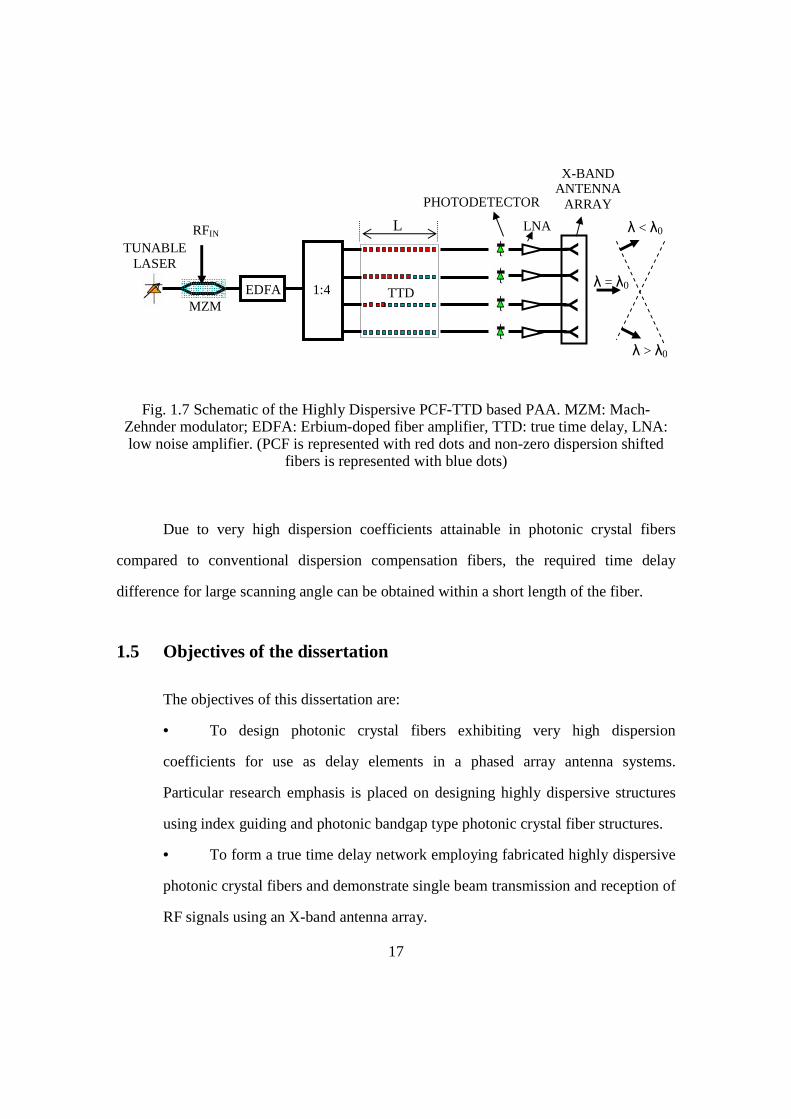
17
Fig. 1.7 Schematic of the Highly Dispersive PCF-TTD based PAA. MZM: Mach-Zehnder modulator; EDFA: Erbium-doped fiber amplifier, TTD: true time delay, LNA: low noise amplifier. (PCF is represented with red dots and non-zero dispersion shifted
fibers is represented with blue dots)
Due to very high dispersion coefficients attainable in photonic crystal fibers
compared to conventional dispersion compensation fibers, the required time delay
difference for large scanning angle can be obtained within a short length of the fiber.
1.5 Objectives of the dissertation
The objectives of this dissertation are:
• To design photonic crystal fibers exhibiting very high dispersion
coefficients for use as delay elements in a phased array antenna systems.
Particular research emphasis is placed on designing highly dispersive structures
using index guiding and photonic bandgap type photonic crystal fiber structures.
• To form a true time delay network employing fabricated highly dispersive
photonic crystal fibers and demonstrate single beam transmission and reception of
RF signals using an X-band antenna array.
X-BAND ANTENNA
ARRAY Y
Y
Y
Y
1:4 EDFA MZM
TUNABLE LASER
TTD
PHOTODETECTOR
LNA RFIN
λ = λ0
λ < λ0
λ > λ0
L

18
• To demonstrate the feasibility of expanding the PAA system to transmit
and receive multiple RF beams and perform an experiment to show simultaneous
dual RF beam transmission and reception of RF signals.
• To evaluate the RF characteristics the X-band PAA system employing
highly dispersive PCF based TTD network by performing harmonic and
intermodulation distortion measurements and to measure the noise figure (NF)
and the spurious-free-dynamic range (SFDR). Efforts are made to improve the
SFDR of the system by employing a high power Erbium-doped fiber amplifier
(EDFA).
• To provide an understanding of the difficulties of forming large practical
antenna arrays and to introduce the concept of sparse arrays. A sparse array is
designed and its working is demonstrated using highly dispersive conventional
dispersion compensation fiber based true-time-delay network.
• To explore the applications of highly dispersive photonic crystal fibers in
other important fields such as pulse compression, soliton propagation etc.
1.6 Dissertation Layout
This dissertation is divided into ten chapters. In Chapter 1, basic concepts of
phased array antennas, phase control methods and an overview of different true-time-
delay techniques are provided. A dispersive fiber prism technique is introduced and the
use of highly dispersive photonic crystal fibers as true-time-delay elements is briefly
discussed. Chapter 2 begins with a brief introduction of photonic crystal fibers. The
central focus of the chapter is on designing highly dispersive photonic crystal fiber
structures. Highly dispersive photonic crystal fiber designs based on index-guidance and
photonic-bandgap guidance mechanisms are presented. The PCF fabrication procedure
19
and the difficulties encountered during the fabrication of such fibers are also briefly
discussed. In Chapter 3, true-time-delay modules formed using a highly dispersive
photonic crystal fiber is presented. The characterization of the highly dispersive photonic
crystal fibers is performed and time delay measurement results of the modules are
presented. In Chapter 4, the formation of a 1x4 X-band phased-array antenna utilizing the
photonic crystal fiber time delay modules is presented in detail. The results for the
demonstration of a single RF beam transmission and reception are presented and
discussed. In Chapter 5, the principle of operation of multiple beam transmission and
reception of the X-band phased-array antenna is introduced. Using the highly dispersive
photonic crystal fiber based true-time-delay modules, simultaneous dual beam
transmission and reception of the phased array antenna system is demonstrated. In
Chapter 6, the effects of noise and distortion on the system performance are briefly
discussed. The Noise Figure (NF), harmonic distortion and intermodulation distortion of
the phased array antenna system are measured. An important parameter describing the
non-linear effects of the system, namely the spurious-free dynamic range (SFDR) is
measured and a method to improve the SFDR is also presented. In Chapter 7, the
practical limitations on the implementation of large phased-array antennas will be briefly
discussed. The concept of a sparse array will be introduced and the feasibility of using the
dispersive fiber prism technique for such systems will be presented and demonstrated
using a true-time-delay network formed using dispersion compensation fibers. In Chapter
8, other important achievements along the way of my research are presented. As a major
achievement, a designed and fabricated photonic crystal fiber exhibiting the highest
dispersion coefficient so far is presented and the practical issues with the fiber are
discussed. The second achievement is the demonstration of the effect of pulse
compression using highly dispersive photonic crystal fiber presented in Chapter 3 by

20
making use of the interplay between dispersive and non-linear effects inside the photonic
crystal fiber. The highly dispersive photonic crystal fiber presented in Chapter 3 is used
in conjunction with a pulsed laser source to demonstrate the effect of pulse compression.
Recommendations for future work such as extending the single and multiple beam
transmission and reception to 2 dimensional phased-array antennas and using highly
dispersive photonic crystal fibers to demonstrate soliton propagation are briefly discussed
in Chapter 9. Finally, in Chapter 10, a summary of the dissertation is given.
1.7 References
[1] H. J. Visser, Array and Phased Array Antenna Basics, John Wiley and Sons Ltd (2005)
[2] C. A. Balanis, Antenna theory: Analysis and design, 3rd Edition, John Wiley & Sons (2005)
[3] R. C. Hansen, Phased array antennas, Wiley-Interscience (1998)
[4] S. Barker and G. M. Rebeiz, “Distributed MEMS true-time delay phase shifters and wide-band switches,” IEEE. Trans. Microwav. Theory. Techniq. vol. 46, pp. 1881 - 1890 (1998)
[5] W. Ng, A. A. Walston, G. L. Tangonan, J. J. Lee, I. L. Newberg, and N. Bernstein, “The first demonstration of an optically steered microwave phased array antenna using true-time-delay,” IEEE. J. Lightwav. Technol. vol. 9, pp. 1124- 1131 (1991)
[6] R. D. Esman, M. Y. Frankel, J. L. Dexter, L. Goldberg, M. G. Parent, D. Stilwell, and D. G. Cooper, “Fiber-optic prism true time-delay antenna feed,” IEEE Photon. Technol. Letts. vol. 11, pp. 1347-1349 (1993)
[7] R. Soref, “Optical dispersion technique for time-delay beam steering,” Appl. Opt. vol. 31, pp. 7395-7397 (1992)
[8] Y. Chen and R. T. Chen, “A fully packaged true time delay module for a K-band phased array antenna system demonstration,” IEEE. Photon. Technol. Letts. vol. 14, pp. 1175 – 1177 (2002)
21
[9] S. Yegnanarayanan and B. Jalali, “Wavelength-selective true time delay for optical control of phased-array antenna,” IEEE. Photon. Technol. Letts. vol. 12, pp. 1049 – 1051 (2000)
[10] D. Dolfi, J. P. Huignard, and M. Baril, “Optically controlled true-time delays for phased array antenna,” Proc. SPIE. vol. 1102, pp. 152 (1989)
[11] D. Dolfi, F. Michel-Gabriel, S. Bann, and J. P. Huignard, “Two-dimensional optical architecture for true-time-delay beam forming in a phased-array antenna,” Opt. Letts. vol. 16, pp. 255-257 (1991)
[12] D. Dolfi, P. Joffre, J. Antoine, J. P. Huignard, D. Philippet, and P. Granger, “Experimental demonstration of a phased-array antenna optically controlled with phase and time delays,” Appl. Opt. vol. 35, pp. 5293-5300 (1996)
[13] N. A. Riza, “Transmit/receive time-delay beam-forming optical architecture for phased-array antennas,” Appl. Opt. vol. 30, pp. 4594-4595 (1991)
[14] N. A. Riza, “Liquid crystal-based optical time delay control system for wideband phased arrays,” Proc. SPIE. vol. 1790, pp. 171-183 (1992)
[15] A. M. Levine, “Use of fiber optic frequency and phase determining element in radar,” in Proceedings of the 33rd Annual Symposium on Frequency Control, IEEE, 436-443 (1979)
[16] P. M. Freitag and S. R. Forrest, “A coherent optically controlled phased array antenna system,” IEEE. Microwav. Guided. Wav. Letts. vol. 3, pp. 293-295 (1993)
[17] L. Xu, R. Taylor, and S. R. Forrest, “True-time delay phased array antenna feed system based on optical heterodyne techniques,” IEEE. Photon. Technol. Letts. vol. 8, pp. 160-162 (1996)
[18] D. K. T. Tong, and M. C. Wu, “A novel multiwavelength optically controlled phased array antenna with a programmable dispersion matrix,” IEEE. Photon. Technol. Letts. vol. 8, pp. 812-814 (1996)
[19] P. Goutzoulis and D. K. Davies, “Hardware-compressive 2-D fiber-optic delay line architecture for time steering of phased-array antennas,” Appl. Opt. vol. 29, pp. 5353-5359 (1990)
[20] P. Goutzoulis and D. K. Davies, “All-optical hardware-compressive wavelength multiplexed fiber optic architecture for true-time delay steering of 2-D phased array antenna,” Proc. SPIE. vol. 1703, pp. 604-614 (1992)
22
[21] P. Goutzoulis and D. K. Davies, J. Zomp, P. Hrycak, and A. Johnson, “Development and field demonstration of a hardware-compressive fiber-optic true time delay steering system for phased array antennas,” Appl. Opt. vol. 33, pp. 8173-8185 (1994)
[22] Z. Fu and R. T. Chen, “Highly packing density optical true-time delay lines for phased array antenna applications,” Recent Research Developments Series, pp. 1, Dec. 1998
[23] S. Yegnanarayanan, P. D. Trinh, and B. Jalali, “Recirculating photonic filter: a wavelength-selective time delay for phased array antennas and wavelength code division multiple access,” Opt. Letts. vol. 21, pp. 740-742 (1996)
[24] W. D. Jemison and P. R. Herczfeld, “Acousto-optically controlled true-time delay,” IEEE. Microwav. Guided Wav. Letts. vol. 3, pp. 72-75 (1993)
[25] L. H. Gesell, R. E. Feinleib, J. L. Lafuse, and T. M. Turpin, “Acousto-optic control of time delays for array beam steering,” Proc. SPIE. vol. 2155, 194 (1994)
[26] E. N. Toughlian and H. Zmuda, “A photonic variable RF delay line for phased array antennas,” IEEE. J. Lightwav. Technol. vol. 8, pp. 1824-1828 (1990)
[27] E. H. Monsay, K. C. Baldwin, and M. J. Caucuitto, “Photonic true-time delay for high-frequency phased array systems,” IEEE. Photon. Technol. Letts. vol. 6, pp. 118-120 (1994)
[28] R. D. Esman, M. J. Monsma, J. L. Dexter, and D. G. Cooper, “Microwave True Time-Delay Modulator Using Fibre-Optic Dispersion,” Electron. Letts. vol. 28, pp. 1905-1907 (1992)
[29] M. Y. Frankel and R. D. Esman, “True time-delay fiber-optic control of an ultra wideband array transmitter/receiver with multibeam capability,” IEEE. Trans. Microwav. Theory. Techniq. vol. 43, pp. 2387–2394 (1995)
[30] S. T. Johns, D. A. Norton, C. W. Keefer, R. Erdmann, and R. A. Soref, “Variable time delay of microwave signals using high dispersion fibre,” Electron. Letts. vol. 29, pp. 555-556 (1993)
[31] J. L. Cruz, B. Ortega, M. V. Andres, B. Gimeno, D. Pastor, J. Capmany, and L. Dong, “Chirped fiber gratings for phased array antenna,” Electron. Letts. vol. 33, pp. 545-546 (1997)
[32] J. L. Corral, J. Marti, S. Regidor, J. M. Fuster, R. Laming, and M. J. Cole, “Continuously variable true time-delay optical feeder for phased-array antenna employing chirped fiber gratings,” IEEE. Trans. Microwav. Theory. Techniq. vol. 45, pp. 1531-1536 (1997)

23
[33] Z. Shi, Y. Jiang, B. Howley, Y. Chen, F. Zhao, and R. T. Chen, "Continuously delay time tunable-waveguide hologram module for X-band phased-array antenna,” IEEE. Photon. Technol. Letts. vol. 15, pp. 972-974 (2003)
[34] Z. Shi, L. Gu, B. Howley, Y. Jiang, Q. Zhou, R. T. Chen, M. Y. Chen, X. Wang, H. R. Fetterman, and G. Brost, “True-time-delay modules based on single tunable laser in conjunction with waveguide-hologram for phased-array antenna,” Opt. Engineering. vol. 44, 084301, (2005)
[35] X. Chen, Z. Shi, L. Gu, B. Howley, Y. Jiang, and R. T. Chen, “Miniaturized Delay time-enhanced Photopolymer Waveguide Hologram Module for Phased-Array Antenna,” IEEE. Photon. Technol. Letts. vol. 17, pp. 2182-2184, (2005)
[36] G. P. Agrawal, Nonlinear Fiber Optics, Academic Press (1995)
[37] K. Thyagarajan, R. K. Varshney, P. Palai, A. K. Ghatak, and I. C. Goyal, “A Novel Design of a Dispersion Compensating Fiber,” IEEE. Photon. Technol. Letts. vol. 8, pp. 1510-1512 (1996)
[38] J. -L. Auguste, R. Jindal, J. -M. Blondy, M. Clapeau, J. Marcou, B. Dussardier, G. Monnom, D. B. Ostrowsky, B. P. Pal, and K. Thyagarajan, “-1800ps/(nm.km) chromatic dispersion at 1.55µm in dual concentric core fibre,” Electron. Letts. vol, pp. 1689-1690 (2000)
[39] Y. Ni, L. Zhang, L. An, J. Peng, and C. Fan, “Dual-Core Photonic Crystal Fiber for Dispersion Compensation,” IEEE. Photon. Technol. Letts. vol. 16, pp. 1516-1518 (2004).
[40] F. Gerome, J. -L. Auguste, and J. –M. Blondy, “Design of dispersion-compensating fibers based on a dual-concentric-core photonic crystal fiber,” Opt. Letts. vol. 29, pp. 2725-2727 (2004)
[41] A. Huttunen, P. Torma, “Optimization of dual-core and microstructure fiber geometried for dispersion compensation and large mode area,” Opt. Express. vol. 13, pp. 627-635 (2005)
[42] P. J. Roberts, B. J. Mangan, H. Sabert, F. Couny, T. A. Birks, J. C. Knight, and P. St. J. Russell, “Control of dispersion in photonic crystal fibers,” J. Opt. Fiber. Commun. Rep. 2, pp. 435-461 (2005)
24
Chapter 2 Highly dispersive photonic crystal fibers
In this chapter, a relatively new kind of fiber called the photonic crystal fiber
(PCF) will be introduced. In such fibers, the structural parameters can be controlled to
tune the dispersion coefficient, which is difficult to achieve in conventional optical fibers.
Two different types of photonic crystal fibers – one having a core made up of solid silica
and the other having an air core will be designed to achieve very high dispersion
coefficients with a potential to be used as true-time-delay (TTD) elements in phased-
array antenna (PAA) systems. Finally, the fabrication method of PCFs will be explained
and difficulties encountered in fabrication will be briefly discussed.
2.1 Photonic Crystal Fiber (PCF)
Photonic crystal fibers (PCF) were first demonstrated by Knight et al. in 1996 [1].
PCFs are very different compared to the conventional single mode fibers. In the
conventional single mode fibers, there is a high refractive index core surrounded by a low
index cladding and light is guided in the core via the principle of total internal reflection
at the core-cladding interface. In a PCF, the uniform cladding of the conventional fibers
is replaced with an array of microscopic air holes that run down the entire length of the
fiber [2, 3]. A defect, usually one or multiple missing holes, acts as core. Due to the
presence of such a cladding, a photonic crystal fiber provides excellent flexibility in
controlling the characteristics of the fiber such as the number of modes, numerical
aperture, dispersion properties, nonlinearity etc by controlling the structural parameters
[1-6]. For example, the dispersion of the PCFs can be flexibly tailored by tuning the pitch
( Λ ) of the periodic array, the air-hole diameter (d) or the refractive index (n) of silica.

25
Highly dispersive PCFs have been proposed for the application of broadband dispersion
compensation in telecommunication [6]. PCFs can also be designed to achieve very high
dispersion coefficients [7-12]. Such highly dispersive photonic crystal fibers have a great
potential for use in phased array antenna systems because they can reduce the size and
weight of the system considerably. The PCFs are also called microstructured fibers, holey
fibers, and photonic bandgap fibers.
2.1.1 TYPES OF PHOTONIC CRYSTAL FIBERS
Depending on the type of guidance in the fibers, PCFs can be classified into [3]
1. Index-guiding PCF
2. Photonic-bandgap PCF
The light guidance mechanism in the index-guiding PCF is very similar to that in
conventional optical fibers, wherein a high index core is surrounded by a relatively lower
index cladding. The scanning electron microscope (SEM) cross section of a fabricated
index-guiding PCF is shown in Fig. 2.1(a) [1]. The core is made up of solid silica and the
cladding is composed of an array of microscopic air holes that run along the axis of the
fiber. The presence of such an air-hole matrix reduces the effective index of the cladding
region. Therefore, similar to the guidance mechanism in conventional optical fibers, the
guidance in this kind of a PCF is due to total internal reflection. By changing the
periodicity (also called pitch) of the air-hole array or the size air-holes in the cladding, the
effective index can be modified and the fiber can exhibit many interesting characteristics
[1-6].
26
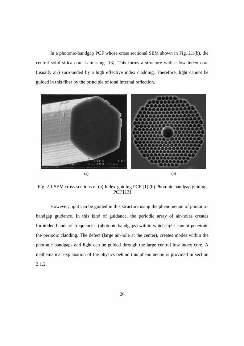
In a photonic-bandgap PCF whose cross sectional SEM shown in Fig. 2.1(b), the
central solid silica core is missing [13]. This forms a structure with a low index core
(usually air) surrounded by a high effective index cladding. Therefore, light cannot be
guided in this fiber by the principle of total internal reflection.
(a) (b)
Fig. 2.1 SEM cross-sections of (a) Index-guiding PCF [1] (b) Photonic bandgap guiding PCF [13]
However, light can be guided in this structure using the phenomenon of photonic-
bandgap guidance. In this kind of guidance, the periodic array of air-holes creates
forbidden bands of frequencies (photonic bandgaps) within which light cannot penetrate
the periodic cladding. The defect (large air-hole at the center), creates modes within the
photonic bandgaps and light can be guided through the large central low index core. A
mathematical explanation of the physics behind this phenomenon is provided in section
2.1.2.

27
2.1.2 MAXWELL ’S EQUATIONS AND BLOCH THEOREM
The set of Maxwell’s electromagnetic equations form the basis for the
development of the theory for photonic bandgap guidance in photonic crystal fibers. The
macroscopic Maxwell’s equation in a dielectric medium under charge-free and current-
free conditions can be written as [3, 14, 15]
0),(
0)),()((
)),(()(),(
)),((),(
0
0
0
=•∇
=•∇∂
∂=×∇
∂∂=×∇
trH
trEr
t
trErtrH
t
trHtrE
vv
vvv
vvvvv
vrvv
εε
εε
µ
(2.1)
whereEr
andHr
are the electrical and magnetic fields, ε is the permittivity, µ is the
permeability, t is time, and r is the displacement to origin.
The time harmonic mode at the steady state is
ti
ti
erEtrE
erHtrHω
ω
−
−
=
=
)(),(
)(),(vvvv
vvvv
(2.2)
By substituting equation (2.2) into equation (2.1), Maxwell equation for the
steady state can be obtained
0))(()(
0))()(()(
0
0
=−×∇
=+×∇
rHirE
rErirHvvvv
vvvvv
µωεεω
(2.3)
28
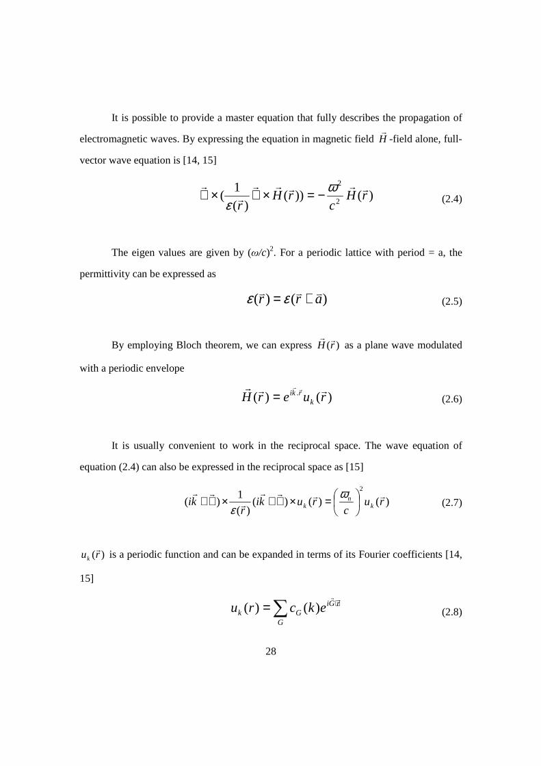
It is possible to provide a master equation that fully describes the propagation of
electromagnetic waves. By expressing the equation in magnetic field Hr
-field alone, full-
vector wave equation is [14, 15]
)())()(
1(
2
2
rHc
rHr
rrrrr
r
r ωε
−=×∇×∇ (2.4)
The eigen values are given by (ω/c)2. For a periodic lattice with period = a, the
permittivity can be expressed as
)()( arrvvv += εε (2.5)
By employing Bloch theorem, we can express )(rHrr
as a plane wave modulated
with a periodic envelope
)()( . ruerH krki rrr rr
= (2.6)
It is usually convenient to work in the reciprocal space. The wave equation of
equation (2.4) can also be expressed in the reciprocal space as [15]
)()()()(
1)(
2
ruc
rukir
ki kn
k
rrrr
r
rr
=×∇+×∇+ω
ε (2.7)
)(ruk
r is a periodic function and can be expanded in terms of its Fourier coefficients [14,
15]
∑ ⋅=G
rGiGk ekcru
rr
)()( (2.8)

29
The transversality condition requires 0)( =•+G
cGk r
rr. We can express
Gc r as the
sum of two components along unit vectors 1e and 2e which are orthogonal to )( Gkrr
+ i.e.
( 2,21,1ˆˆ ececc
GGGrrr += ) [3]. By substituting equation (2.8) in equation (2.7) and taking the
Fourier transform on both sides, we get [15]
[ ] '2
21
,' )()'( GGG
GG cc
cGkGkωε =×+×+⋅−∑ −
− (2.9)
Equation (2.9) can be solved using Fast Fourier Transform techniques and
compute the set of cG’s by using a finite and a large number of plane waves. The
eigensolutions are periodic functions of Bloch wavevector k. This method of solving is
also called the plane wave expansion (PWE) [3]
2.2 Design of highly dispersive photonic crystal fibers
Conventional fibers designed for dispersion compensation in optical
communication have shown that high values of dispersion coefficients (D ~ -100
ps/nm/km) can be achieved [5, 16]. However, the dispersion cannot be changed
significantly in such fibers due to the small index variation across the transverse cross
section of the fiber from doping.
Due to the presence of an array of periodic air holes running down the length in a
photonic crystal fiber, index variations across the transverse cross section by changing
the structural parameters such as air-hole diameter, periodicity etc is highly feasible.
Therefore, PCFs have gained increasing popularity over the recent years due to their
unique properties such as endless single mode operation [17], high nonlinearity [18], and

30
ultralow loss [19, 20] etc. It has been shown that photonic crystal fibers, unlike
conventional dispersion compensation fibers (DCF) can be designed to exhibit extremely
high dispersion coefficients [6, 8, 9, 10, 11, 12, 21, 22, 23]. Extreme values of dispersion
coefficient as large as -59000ps/nm/km have been predicted [8] for geometries based on
dual-core structure using a doped core. However, this comes at the expense of extremely
narrow bandwidth. Although such highly dispersive photonic crystal fibers can be used
for phased array antenna application, due to their extremely narrow bandwidth, the
steering angle becomes extremely difficult to control. Therefore, there is a need to
fabricate highly dispersive PCF structures that exhibit high dispersion and modest
bandwidth (high dispersion-bandwidth product) for use as true-time-delay modules in
phased array antenna systems. As stated earlier in section 1.4, the employment of such
highly dispersive PCFs helps in reducing the size and weight of the system when used in
a true-time-delay network, leading to compact device structures suitable for air-borne and
space-borne applications.
2.2.1 HIGHLY DISPERSIVE STRUCTURE BASED ON INDEX -GUIDING PCF
It is possible to design highly dispersive structures based on index-guiding PCFs.
The structure of the highly dispersive photonic crystal fiber is based on dual concentric-
core design as proposed by Thyagarajan et al. in the year 1996 [9]. The working principle
of this structure is similar to that of a directional coupler [24]. In this section, the working
principle of a dual concentric-core photonic crystal fiber and design results demonstrating
very high dispersion and bandwidth will be presented.

31
2.2.1.1 Working principle of a highly dispersive PCF based on a dual concentric-core design
The working mechanism of a dual concentric-core PCF is very similar to that of a
directional coupler which can support two supermodes [24]. First, we introduce the
coupled mode theory on the dual core PCFs [22]. The central core and the outer core
behave like two parallel waveguides and the high dispersion is from the coupling
between the two waveguides. We can expand the propagation constants, β, of the modes
in the isolated waveguides around the phase matched frequency using Taylor’s series and
neglect higher order terms to get [24]
pp
d
d
d
d ipippi
ωωωω ωβωω
ωβωωωβωβ
==
−+−+≈
2
22
2
)()()()( (2.10)
where i = 1, 2 represents the inner and the outer waveguide respectively and pω
represents the phase matched frequency.
The coupled mode theory tells us that the coupling of individual modes can
generate two supermodes, whose propagation constants can be written as [24, 25]
4)(2)(
2/)(
2/)(
222
21
221
210
21
2200
ββκβββββ
ββδδκβγβ
−+±+=⇒
+=−=
+±=+=
±
±
B
B n
(2.11)
where κ is the coupling constant between the two waveguides. 1β and 2β are the
propagation constants of the inner and outer cores respectively.
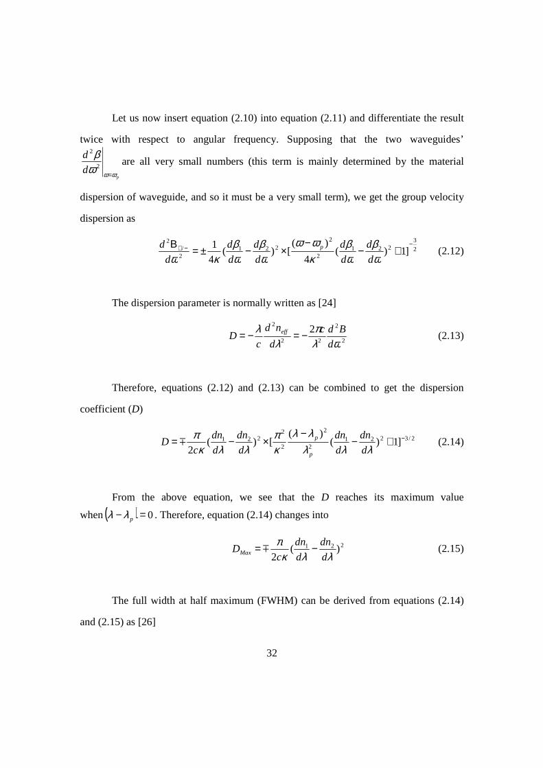
32
Let us now insert equation (2.10) into equation (2.11) and differentiate the result
twice with respect to angular frequency. Supposing that the two waveguides’
pd
d
ωωωβ
=2
2
are all very small numbers (this term is mainly determined by the material
dispersion of waveguide, and so it must be a very small term), we get the group velocity
dispersion as
2
3221
2
2221
2/
2
]1)(4
)([)(
4
1 −−+ +−
−×−±=Β
ωβ
ωβ
κωω
ωβ
ωβ
κω d
d
d
d
d
d
d
d
d
d p (2.12)
The dispersion parameter is normally written as [24]
2
2
22
22
ωλπ
λλ
d
Bdc
d
nd
cD eff −=−= (2.13)
Therefore, equations (2.12) and (2.13) can be combined to get the dispersion
coefficient (D)
2/32212
2
2
2221 ]1)(
)([)(
2−+−
−×−=
λλλλλ
κπ
λλκπ
d
dn
d
dn
d
dn
d
dn
cD
p
pm (2.14)
From the above equation, we see that the D reaches its maximum value
when( ) 0=− pλλ . Therefore, equation (2.14) changes into
221 )(2 λλκπ
d
dn
d
dn
cDMax −= m (2.15)
The full width at half maximum (FWHM) can be derived from equations (2.14)
and (2.15) as [26]
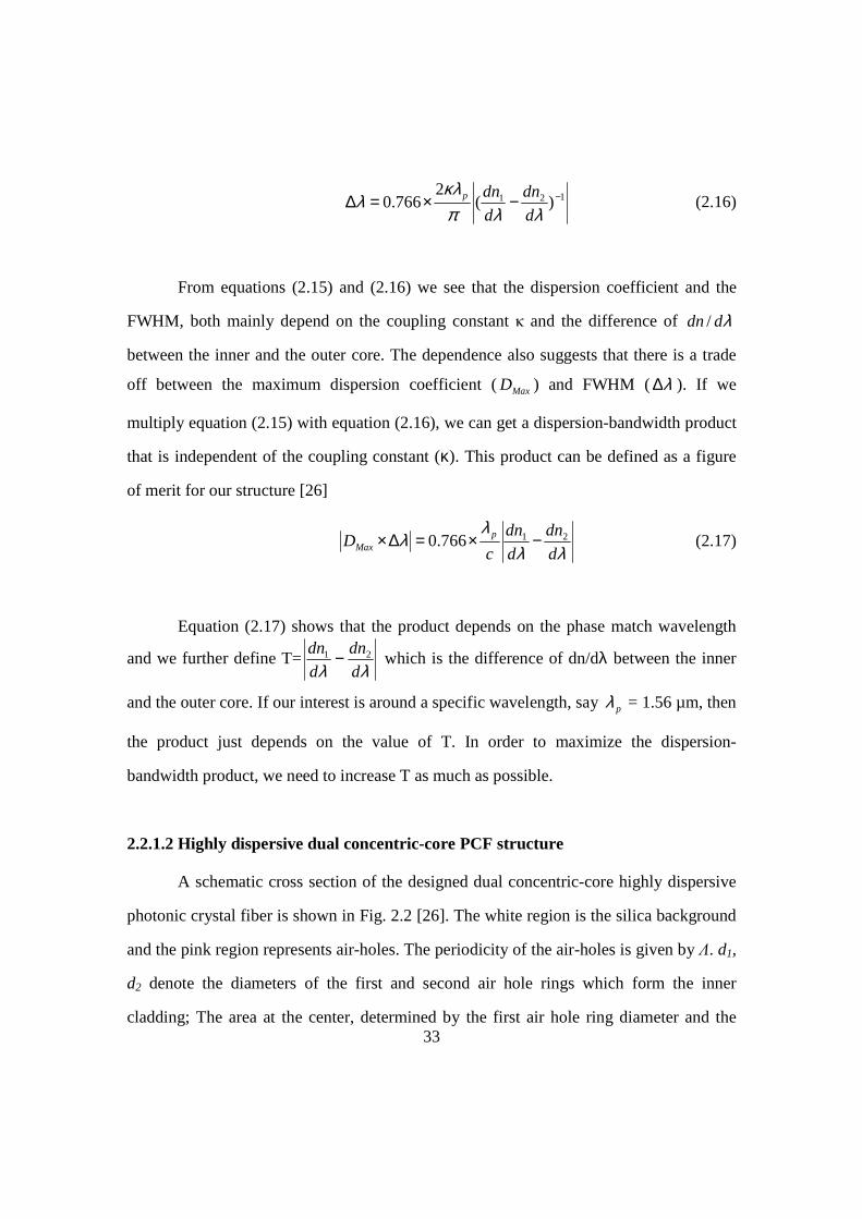
33
121 )(2
766.0 −−×=∆λλπ
κλλ
d
dn
d
dnp (2.16)
From equations (2.15) and (2.16) we see that the dispersion coefficient and the
FWHM, both mainly depend on the coupling constant κ and the difference of λddn/
between the inner and the outer core. The dependence also suggests that there is a trade
off between the maximum dispersion coefficient (MaxD ) and FWHM ( λ∆ ). If we
multiply equation (2.15) with equation (2.16), we can get a dispersion-bandwidth product
that is independent of the coupling constant (κ). This product can be defined as a figure
of merit for our structure [26]
λλ
λλ
d
dn
d
dn
cD p
Max21766.0 −×=∆× (2.17)
Equation (2.17) shows that the product depends on the phase match wavelength
and we further define T=λλ d
dn
d
dn 21 − which is the difference of dn/dλ between the inner
and the outer core. If our interest is around a specific wavelength, say pλ = 1.56 µm, then
the product just depends on the value of T. In order to maximize the dispersion-
bandwidth product, we need to increase T as much as possible.
2.2.1.2 Highly dispersive dual concentric-core PCF structure
A schematic cross section of the designed dual concentric-core highly dispersive
photonic crystal fiber is shown in Fig. 2.2 [26]. The white region is the silica background
and the pink region represents air-holes. The periodicity of the air-holes is given by Λ. d1,
d2 denote the diameters of the first and second air hole rings which form the inner
cladding; The area at the center, determined by the first air hole ring diameter and the

34
period, forms the center core; d3 denotes the diameter of the third air hole ring which
forms the second core. The rest of the air hole rings (fourth-tenth rings) form the outer
cladding region. The research work presented herein has the highest value dispersion-
bandwidth product reported thus far [26]. It also has high dispersion value which is an
improvement by a factor of 5 over previous designs and is a promising candidate for
applications requiring compact systems for broadband phased array antennas.
Fig. 2.2 Schematic cross section of the designed dual concentric core PCF
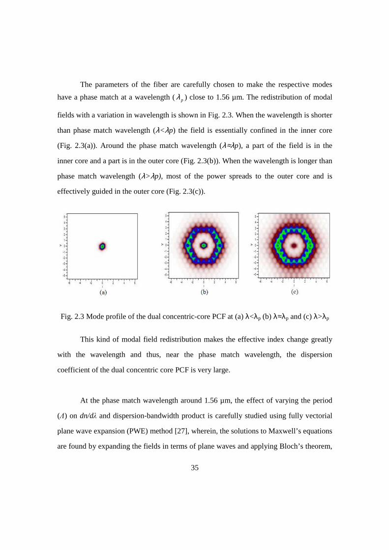
35
The parameters of the fiber are carefully chosen to make the respective modes
have a phase match at a wavelength (pλ ) close to 1.56 µm. The redistribution of modal
fields with a variation in wavelength is shown in Fig. 2.3. When the wavelength is shorter
than phase match wavelength (λ<λp) the field is essentially confined in the inner core
(Fig. 2.3(a)). Around the phase match wavelength (λ≈λp), a part of the field is in the
inner core and a part is in the outer core (Fig. 2.3(b)). When the wavelength is longer than
phase match wavelength (λ>λp), most of the power spreads to the outer core and is
effectively guided in the outer core (Fig. 2.3(c)).
Fig. 2.3 Mode profile of the dual concentric-core PCF at (a) λ<λp (b) λ≈λp and (c) λ>λp
This kind of modal field redistribution makes the effective index change greatly
with the wavelength and thus, near the phase match wavelength, the dispersion
coefficient of the dual concentric core PCF is very large.
At the phase match wavelength around 1.56 µm, the effect of varying the period
(Λ) on dn/dλ and dispersion-bandwidth product is carefully studied using fully vectorial
plane wave expansion (PWE) method [27], wherein, the solutions to Maxwell’s equations
are found by expanding the fields in terms of plane waves and applying Bloch’s theorem,
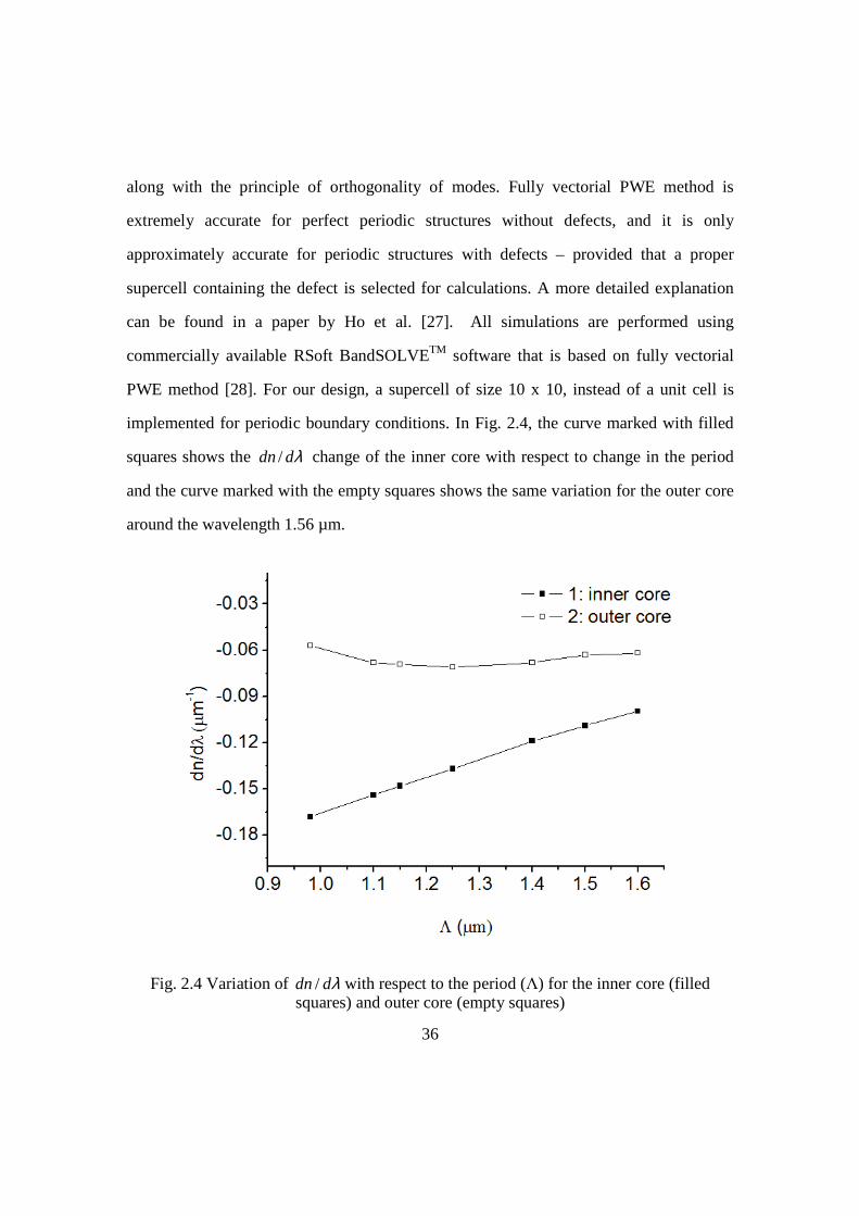
36
along with the principle of orthogonality of modes. Fully vectorial PWE method is
extremely accurate for perfect periodic structures without defects, and it is only
approximately accurate for periodic structures with defects – provided that a proper
supercell containing the defect is selected for calculations. A more detailed explanation
can be found in a paper by Ho et al. [27]. All simulations are performed using
commercially available RSoft BandSOLVETM software that is based on fully vectorial
PWE method [28]. For our design, a supercell of size 10 x 10, instead of a unit cell is
implemented for periodic boundary conditions. In Fig. 2.4, the curve marked with filled
squares shows the λddn/ change of the inner core with respect to change in the period
and the curve marked with the empty squares shows the same variation for the outer core
around the wavelength 1.56 µm.
Fig. 2.4 Variation of λddn/ with respect to the period (Λ) for the inner core (filled squares) and outer core (empty squares)
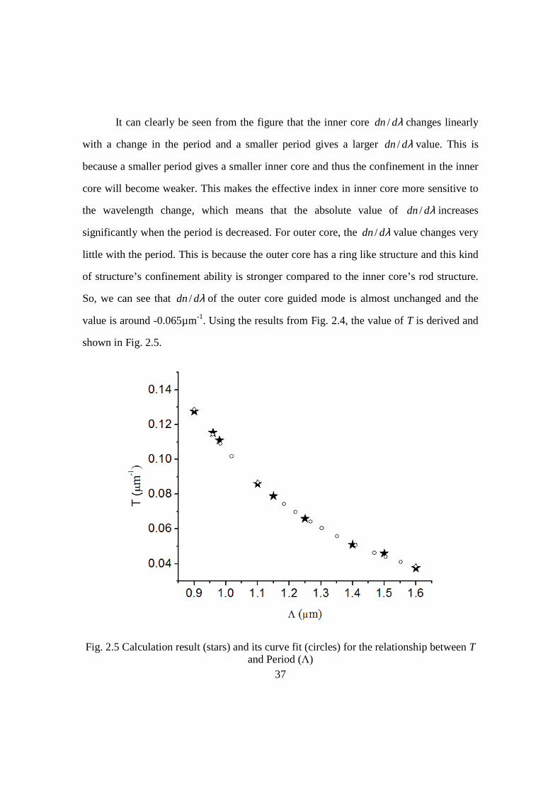
37
It can clearly be seen from the figure that the inner core λddn/ changes linearly
with a change in the period and a smaller period gives a larger λddn/ value. This is
because a smaller period gives a smaller inner core and thus the confinement in the inner
core will become weaker. This makes the effective index in inner core more sensitive to
the wavelength change, which means that the absolute value of λddn/ increases
significantly when the period is decreased. For outer core, the λddn/ value changes very
little with the period. This is because the outer core has a ring like structure and this kind
of structure’s confinement ability is stronger compared to the inner core’s rod structure.
So, we can see that λddn/ of the outer core guided mode is almost unchanged and the
value is around -0.065µm-1. Using the results from Fig. 2.4, the value of T is derived and
shown in Fig. 2.5.
Fig. 2.5 Calculation result (stars) and its curve fit (circles) for the relationship between T and Period (Λ)

38
It can be seen from the figure that the value of T decreases with an increase in the
value of the period and this is mainly contributed by the inner core’s λddn/ change. The
curve marked with stars is the calculation result and the curve marked with circles is a fit
to the calculation result. It is found that the value of T decays exponentially with an
increase in the period of the holes and the decay constant is about 0.431µm. This result
combined with equation (2.17) also means that the dispersion-bandwidth product decays
exponentially as the period is increased.
From the above discussion we find that the period (Λ) plays a vital role in
achieving broadband operation along with a very high dispersion value. By designing
PCF structures with very small air-hole pitch, we can achieve very high dispersion-
bandwidth products. However, it becomes very difficult, in practice, to control the
diameter of the air holes over such small dimensions. As will be discussed in section
2.3.2, by choosing a value of period as 0.98 µm, we are almost hitting the limits of
manufacturability. In order to satisfy the high dispersion-bandwidth requirement and
manufacturing feasibility simultaneously, a dual concentric-core pure silica PCF with
mµ98.0=Λ is designed to have a maximum dispersion value of about
kmnmps //9500− and bandwidth of about 55 nm. The inner core is made of pure silica,
surrounded by an inner cladding made of two air hole rings with of diameter d1, followed
by an outer core with diameter d2, and then by an outer cladding with diameter d3. Since
we are hitting the limit of manufacturability at a period of 0.98 µm, we choose this value
for period and simulate structures with various parameter values. The fabrication
difficulties are discussed later in this chapter. A structure with values of d1/Λ = 0.90, d2/Λ
= 0.59, and d3/Λ = 0.76, is chosen in order to provide a maximum dispersion coefficient
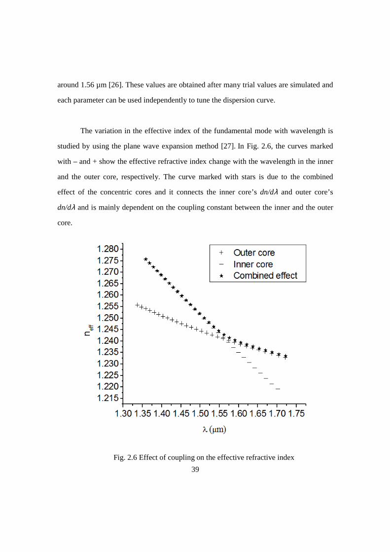
39
around 1.56 µm [26]. These values are obtained after many trial values are simulated and
each parameter can be used independently to tune the dispersion curve.
The variation in the effective index of the fundamental mode with wavelength is
studied by using the plane wave expansion method [27]. In Fig. 2.6, the curves marked
with – and + show the effective refractive index change with the wavelength in the inner
and the outer core, respectively. The curve marked with stars is due to the combined
effect of the concentric cores and it connects the inner core’s dn/dλ and outer core’s
dn/dλ and is mainly dependent on the coupling constant between the inner and the outer
core.
Fig. 2.6 Effect of coupling on the effective refractive index

40
This curve predominantly controls the shape of the resulting dispersion curve. We
can also see that the two individual core curves are like the asymptotes to the combined
curve. This means that, for a wavelength greater than the phase match wavelength, the
mode is just like being confined in the outer core and can not feel any effect from the
inner core and vice versa. In order to use equation (2.13) to calculate the net chromatic
dispersion of the structure, we perform a second differential on the curve marked with
stars with respect to the wavelength and multiply the by -λ/c. The result of our
calculation is shown in Fig. 2.7 as a curve marked with solid squares. From the figure, we
see that the maximum value of dispersion achieved is around -9500ps/nm/km and the
FWHM is about 55nm near a wavelength of 1.56µm.
Fig. 2.7 Relationship between the dispersion value D and wavelength and comparison of Plane Wave Expansion (filled squares) and Coupled-Mode Theory (empty circles) results

41
Finite Difference Beam Propagation Method (BPM) [28-30] is used to calculate
the two mode patterns in the inner and the outer core and an overlap integral method is
used to calculate the coupling constant between the two cores. All the simulations
performed above are done using RSoft BeamPROPTM software package [28]. The
software can compute the mode patterns, given a refractive index profile and an input
field. The coupling factor is also computed and is found to be, κ=2π*0.00167/λp=0.00673
µm-1. Coupled mode theory is employed to obtain the curve between the dispersion and
the wavelength. The plane wave expansion [27] is compared with that of the coupled
mode theory [29] in Fig. 2.7 and the results are found to be in good agreement with each
other. This kind of broadband, highly negative dispersion fiber can be used in radar
applications.
In order to see the effect of these parameters on the dispersion curve, each
parameter is varied independently, while keeping the remaining parameters at the above
mentioned values and the results are shown in Fig. 2.8. The dependence of dispersion on
Λ is shown in Fig. 2.8(a). As discussed previously, it can be seen that the value of
dispersion decreases as the period is increased. The dip also changes its position on the
wavelength scale. The dependence of the position and magnitude of the dispersion curve
on d1, d2, and d3 are shown in Figs. 2.8(b), 2.8(c) and 2.8(d) respectively. It can be seen
from these figures that the position and magnitude of the dispersion curve is extremely
sensitive to the parameter values, therefore the parameters need to be strictly controlled
while drawing the fibers making fabrication even more challenging. This issue also sets a
limit on the manufacturability.
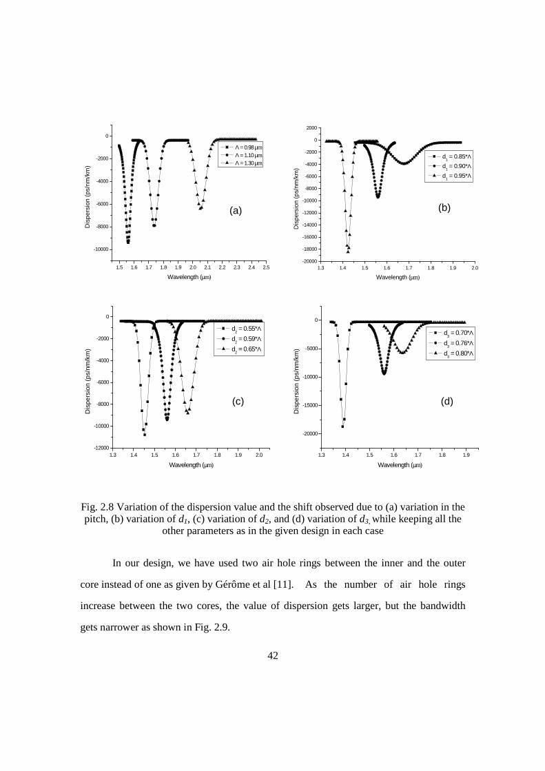
42
Fig. 2.8 Variation of the dispersion value and the shift observed due to (a) variation in the pitch, (b) variation of d1, (c) variation of d2, and (d) variation of d3, while keeping all the
other parameters as in the given design in each case
In our design, we have used two air hole rings between the inner and the outer
core instead of one as given by Gérôme et al [11]. As the number of air hole rings
increase between the two cores, the value of dispersion gets larger, but the bandwidth
gets narrower as shown in Fig. 2.9.
1.3 1.4 1.5 1.6 1.7 1.8 1.9 2.0-12000
-10000
-8000
-6000
-4000
-2000
0
Dis
pers
ion
(ps/
nm/k
m)
Wavelength (µm)
d2 = 0.55*Λ
d2 = 0.59*Λ
d2 = 0.65*Λ
1.3 1.4 1.5 1.6 1.7 1.8 1.9 2.0-20000
-18000
-16000
-14000
-12000
-10000
-8000
-6000
-4000
-2000
0
2000
Dis
pers
ion
(ps/
nm/k
m)
Wavelength (µm)
d1 = 0.85*Λ
d1 = 0.90*Λ
d1 = 0.95*Λ
1.3 1.4 1.5 1.6 1.7 1.8 1.9
-20000
-15000
-10000
-5000
0
Dis
pers
ion
(ps/
nm/k
m)
Wavelength (µm)
d3 = 0.70*Λ
d3 = 0.76*Λ
d3 = 0.80*Λ
(a) (b)
(c) (d)
1.5 1.6 1.7 1.8 1.9 2.0 2.1 2.2 2.3 2.4 2.5
-10000
-8000
-6000
-4000
-2000
0
Dis
pers
ion
(ps/
nm/k
m)
Wavelength (µm)
Λ = 0.98 µm Λ = 1.10 µm Λ = 1.30 µm
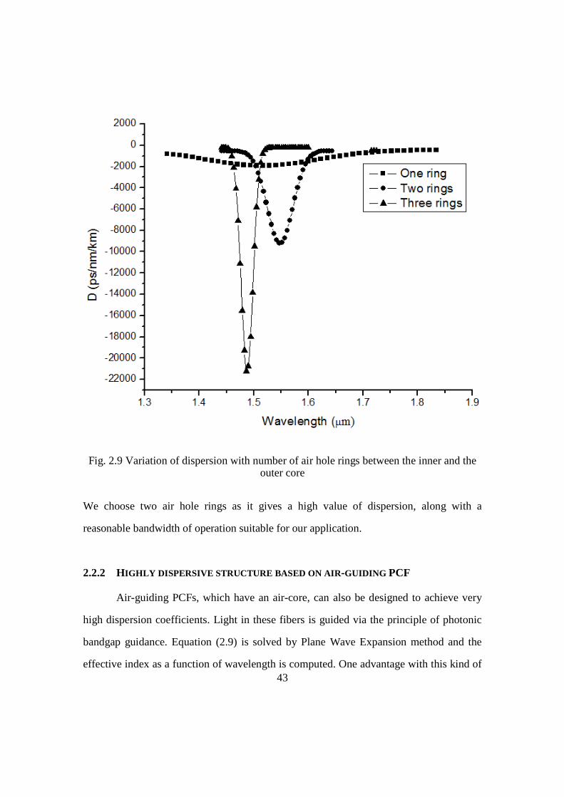
43
Fig. 2.9 Variation of dispersion with number of air hole rings between the inner and the outer core
We choose two air hole rings as it gives a high value of dispersion, along with a
reasonable bandwidth of operation suitable for our application.
2.2.2 HIGHLY DISPERSIVE STRUCTURE BASED ON AIR -GUIDING PCF
Air-guiding PCFs, which have an air-core, can also be designed to achieve very
high dispersion coefficients. Light in these fibers is guided via the principle of photonic
bandgap guidance. Equation (2.9) is solved by Plane Wave Expansion method and the
effective index as a function of wavelength is computed. One advantage with this kind of

44
a structure is that very high power light can be guided through these fibers as there is
very little interaction of light with glass. Therefore, the damage threshold of the fibers is
very high. Such photonic bandgap fibers also exhibit very high dispersion coefficient
values near the band edges as a consequence of Kramers-Kronig relation. The dispersion
coefficient of such fibers is negative at shorter wavelengths, passes through zero and then
assumes positive values at higher wavelengths within the bandgap.
A photonic bandgap fiber with a hexagonal lattice is very easy to fabricate. Such a
structure provides a very high air-filling fraction. A high air-filling fraction opens the
band gap even more, thus increasing the bandwidth of the fiber. By introducing a defect,
such as an air-core in an otherwise perfectly periodic lattice, defect modes are created
inside the photonic bandgap. Light satisfying the defect mode criterion cannot propagate
into the periodic cladding as it is within the photonic bandgap (forbidden frequency band)
of the periodic cladding. Therefore, light propagates through the defect (air-core) without
much interaction with the surrounding silica lattice. Near the band edges, the
transmission abruptly drops and light is no longer within the forbidden region of the
periodic cladding. There is a sudden change in the effective refractive index of the mode,
and hence, a steep increase in the dispersion coefficient is observed near the band edges.
The schematic of the cross section of the designed photonic bandgap fiber
structure exhibiting a very high value of dispersion coefficient near 1550nm is shown in
Fig. 2.10. The red region is the silica background and the white regions denote air. It can
be seen from the figure that the structure consists of a periodic cladding made up of
closely packed hexagonal shaped holes.
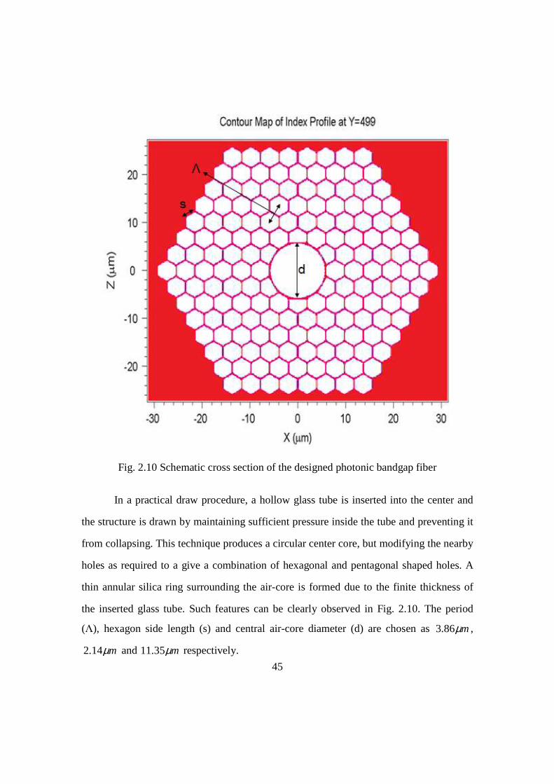
45
Fig. 2.10 Schematic cross section of the designed photonic bandgap fiber
In a practical draw procedure, a hollow glass tube is inserted into the center and
the structure is drawn by maintaining sufficient pressure inside the tube and preventing it
from collapsing. This technique produces a circular center core, but modifying the nearby
holes as required to a give a combination of hexagonal and pentagonal shaped holes. A
thin annular silica ring surrounding the air-core is formed due to the finite thickness of
the inserted glass tube. Such features can be clearly observed in Fig. 2.10. The period
(Λ), hexagon side length (s) and central air-core diameter (d) are chosen as mµ86.3 ,
mµ14.2 and mµ35.11 respectively.

46
Using the formalism in section 2.1.2, the periodic boundary valued problem can
be solved using PWE method. RSoft BandSOLVETM software is used to compute the
bandgaps exhibited by the periodic cladding. The solutions to the periodic cladding
problem are plotted (blue) on the frequency versus propagation constant as shown in Fig.
2.11(a).
Fig. 2.11 (a) Frequency versus propagation constant relation for the cladding showing forbidden regions (gap) within which no solution to Maxwell’s equations exists (b) The
gap edges are plotted showing the light line (frequency = propagation constant)
47
The discrete lines are due to discrete steps used in defining the propagation
constant in the software. It can be seen from the figure that there is a frequency range for
certain propagation constants within which no solutions to Maxwell’s equations exists.
These forbidden frequency ranges, also called bandgaps, are regions within which light
cannot propagate through the cladding. The bandgap edges along with the light line
(slope = unity) is also shown in Fig. 2.11(b). The light line is important for our
application because the central core (defect) is made of air. Due to the inclusion of such a
defect, thousands of defect modes (solutions to Maxwell’s equations) exist within the
bandgap. It becomes necessary to filter out the unnecessary modes and only extract the
useful modes. We know that since the light mode propagates through air-core, the modal
index is very close to unity. Therefore, the probability of finding a useful mode very
close to the light line becomes very high. Using such a condition, the software can be
used to extract useful modes and provide solutions.
As was in the previous case of index guiding PCF fiber, in order to simulate the
dispersion curves of such a structure, a super cell needs to be chosen as the structure has a
defect (central air-core). A 10 x 10 supercell satisfies the periodic boundary conditions.
The fiber supports fundamental modes which have a near-Gaussian profile as shown in
Fig. 2.12 (a). The higher order modes are also shown in Fig. 2.12 (b) and Fig. 2.12 (c).
The calculated effective refractive index of the fundamental mode as a function of
wavelength is shown in Fig. 2.13.
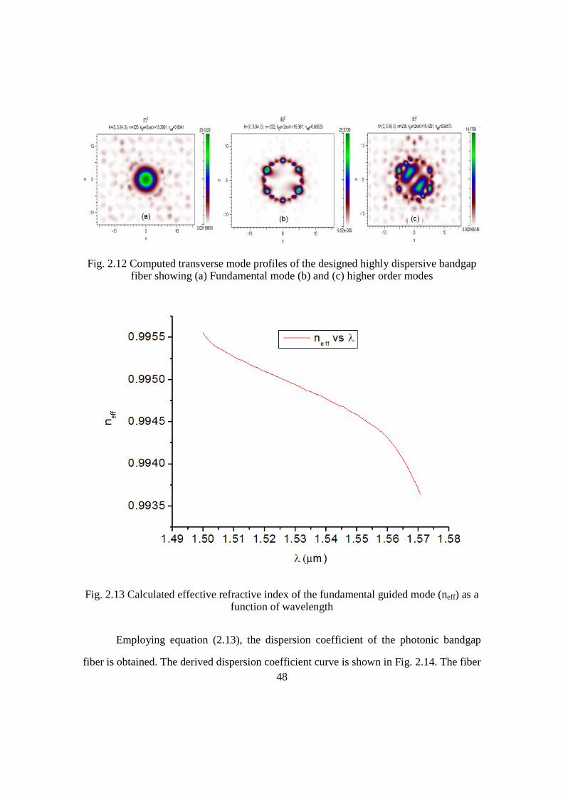
48
Fig. 2.12 Computed transverse mode profiles of the designed highly dispersive bandgap fiber showing (a) Fundamental mode (b) and (c) higher order modes
Fig. 2.13 Calculated effective refractive index of the fundamental guided mode (neff) as a function of wavelength
Employing equation (2.13), the dispersion coefficient of the photonic bandgap
fiber is obtained. The derived dispersion coefficient curve is shown in Fig. 2.14. The fiber
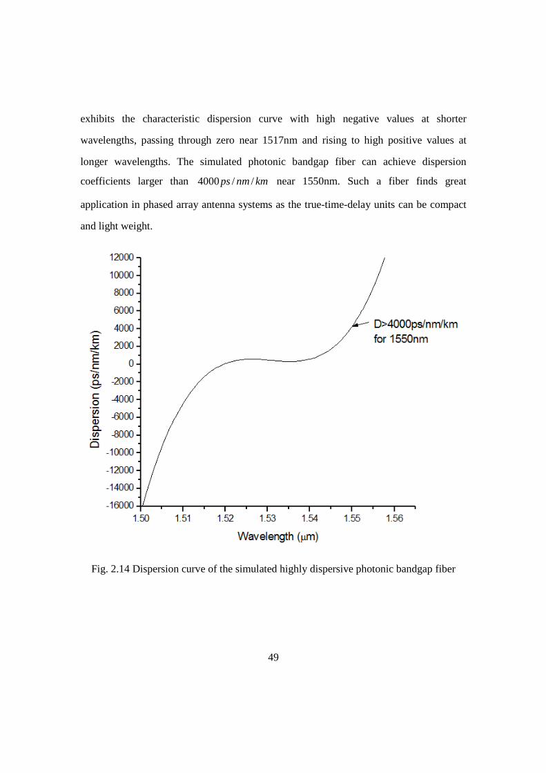
49
exhibits the characteristic dispersion curve with high negative values at shorter
wavelengths, passing through zero near 1517nm and rising to high positive values at
longer wavelengths. The simulated photonic bandgap fiber can achieve dispersion
coefficients larger than kmnmps //4000 near 1550nm. Such a fiber finds great
application in phased array antenna systems as the true-time-delay units can be compact
and light weight.
Fig. 2.14 Dispersion curve of the simulated highly dispersive photonic bandgap fiber
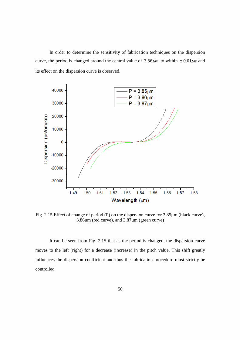
50
In order to determine the sensitivity of fabrication techniques on the dispersion
curve, the period is changed around the central value of mµ86.3 to within mµ01.0± and
its effect on the dispersion curve is observed.
Fig. 2.15 Effect of change of period (P) on the dispersion curve for 3.85µm (black curve), 3.86µm (red curve), and 3.87µm (green curve)
It can be seen from Fig. 2.15 that as the period is changed, the dispersion curve
moves to the left (right) for a decrease (increase) in the pitch value. This shift greatly
influences the dispersion coefficient and thus the fabrication procedure must strictly be
controlled.

51
2.2.3 OTHER HIGHLY DISPERSIVE PCF STRUCTURES
By introducing an additional air hole at the center with diameter d4, it is possible
to tune the refractive index of the central core. By choosing simulation parameters as
mµ1.1=Λ , Λ
1d= 0.94,
Λ2d
= 0.64, Λ
3d= 0.76, and
Λ4d
= 0.2, it is possible to obtain a
broader bandwidth dispersion curve as shown in Fig. 2.16 (cross section of the designed
fiber is also shown). However, this structure exhibits a lower dispersion coefficient
compared to the structure described in section 2.1. The structure exhibits a dispersion
coefficient as large as kmnmps //2500− at 1550nm and has a FWHM of ~200nm.
Fig. 2.16 Dispersion coefficient for PCF structure with a small air-hole at the center (cross section of the designed fiber is also shown)
Apart from using an all-silica photonic crystal fiber structure to achieve high
dispersion bandwidth, the inner and outer cores can be doped to increase (Germanium
Dioxide doping) or decrease (Fluorine doping) the refractive index with respect to

52
background silica. A higher refractive index contrast between the inner and outer core
provides a larger dispersion coefficient. By properly choosing the parameters as Λ = 2.51
microns, Λ
1d = 0.85,
Λ2d
= 0.73, Λ
3d = 0.80,
Λ4d
= 0.40 and doping the inner and outer
cores to achieve change in refractive index (n∆ ) as 1.35% and -0.7% respectively, a very
high dispersion coefficient of kmnmps //5500− at 1553nm is achieved as shown in Fig.
2.17. The FWHM of the structure is ~20nm. However, introducing dopants to increase of
decrease the refractive index creates more scattering locations and this greatly affects the
performance of the system in terms of loss.
Fig. 2.17 Dispersion coefficient for PCF structure with doping-induced refractive index change of the cores

53
2.3 Fabrication of photonic crystal fibers
In this section, the fabrication technique of photonic crystal fibers is described.
Difficulties encountered during fabrication and practical design considerations are also
discussed.
2.3.1 STACK AND DRAW TECHNIQUE
PCFs can be fabricated using stack and draw [3, 31, 32], extrusion [34, 35] and
drilling [33] techniques. Extrusion and drilling techniques are used for soft glasses and
polymers. The stack and draw technique is the most widely used method, and hence will
be described in this section. The fabrication of PCF is similar to that of a conventional
fiber fabrication method. A schematic of the fabrication procedure is shown in Fig. 2.18
[36].
Fig. 2.18 Schematic of stack and draw method for fabricating photonic crystal fibers [36]
High purity silica tubes with different diameters and thicknesses can be used to
determine the pitch and diameter of air holes. These tubes, which have an initial diameter

54
of about 5mm, are heated to temperatures between 12000-18000C and drawn down to
capillaries with a diameter of about 1mm as shown in Fig. 2.18(a). In the next step,
multiple individual capillaries are stacked by hand to create a preform with the required
structure as shown in Fig. 2.18(b). The center core is usually a solid rod (for index-
guiding PCF) or air-hole with suitable diameter at the center (for photonic bandgap PCF).
It is also possible to create additional defect locations using the stack technique. Once the
structure is realized, the stack is fused and drawn down to an overall diameter of about
2mm to kilometer lengths in a fiber draw tower at high temperatures as shown in Fig.
2.18(c). Finally, a polymer coating is added to increase the strength and drawn down to a
final diameter of about 0.1mm as shown in Fig. 2.18(d). In the entire process, the draw
parameters (like pressure, speed etc) are carefully controlled to prevent the air-holes from
deforming or collapsing. The size and shape of air-holes are closely monitored as the
fiber is drawn. This method provides a great deal of design flexibility, since the core size,
air-hole diameters, shape and the index profile throughout the fiber can be controlled.
2.3.2 FABRICATION DIFFICULTIES
The main problems that are encountered during fabrication are presence of
deformed air-holes, generation of additional holes, and changes in the structure’s
symmetry [37]. During fabrication, a number of factors contribute to the deviation of the
final PCF structure from the desired one. Such deviations can greatly influence the
properties of the resulting PCF. As the capillary stack is drawn to form the PCF structure,
the walls of capillaries also shrink. If however, the wall thickness is small, then surface
tension (usually exerted due to outer coating) and high viscosity of glass at low
temperature acts to deform the circular shape. The thin walls, under the influence of
neighboring capillaries adopt a shape that corresponds to the symmetry of the cladding

55
region and deform away from a circle. For example, if the wall thickness is too thin is a
hexagonal cladding lattice, then the individual circular holes deform and assume a
hexagonal shape. Although this is advantageous for certain kinds of desired photonic
bandgap fibers, it is not a desirable effect for other structures. Therefore, it is not
practically feasible to control the shape of air holes when the ratio of air-hole diameter to
pitch (d/Λ) is greater than 0.8. The shape of the air holes can also be well controlled
when the pitch is at least greater than or equal to mµ98.0 , although pitch greater than
mµ2 is highly recommended.
It is also difficult to control the shape of the air-holes because the effects of
surface tension and viscosity of glass tend to collapse the air-holes. The large interstitial
holes are avoided by fusion and inclusion of fine fibers in the interstices before drawing.
The shape of the air-holes depends on temperature distribution, which has a radial profile.
This causes outer holes to be more deformed compared to the inner holes. Therefore,
extra rings of capillaries need to be added to prevent this. The additional rings do not
affect the optical mode guided in the core [37]. During the fabrication process,
microscopic sized holes are controlled by adjusting the temperature and drawing rate. In
order to alleviate the effects of air-hole closure, the air-holes can be pressurized [38]. It is
possible to control the shape of air holes by controlling the pressure. In structures
requiring more than 3 different air-hole sizes, it becomes very difficult to control the
diameters as three different sized capillaries with different wall thicknesses are stacked to
form the perform. Also, it is difficult to obtain an optimum operating point when a large
number of air-hole sizes are required.
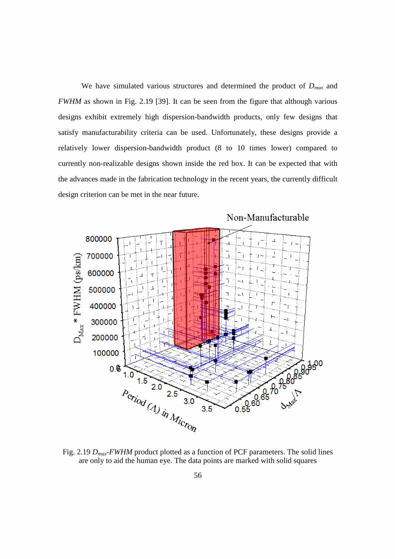
56
We have simulated various structures and determined the product of Dmax and
FWHM as shown in Fig. 2.19 [39]. It can be seen from the figure that although various
designs exhibit extremely high dispersion-bandwidth products, only few designs that
satisfy manufacturability criteria can be used. Unfortunately, these designs provide a
relatively lower dispersion-bandwidth product (8 to 10 times lower) compared to
currently non-realizable designs shown inside the red box. It can be expected that with
the advances made in the fabrication technology in the recent years, the currently difficult
design criterion can be met in the near future.
Fig. 2.19 Dmax-FWHM product plotted as a function of PCF parameters. The solid lines are only to aid the human eye. The data points are marked with solid squares
57
2.4 Summary
In this chapter, photonic crystal fibers were introduced and the working principle
of two kinds of photonic crystal fibers was explained. Working principle of a highly
dispersive photonic crystal fiber with a dual concentric-core was presented and a PCF
structure was designed to exhibit a very high dispersion coefficient of kmnmps //9500−
close to 1550nm and a FWHM of 55nm. Another photonic crystal fiber based on
photonic bandgap guidance was also designed to achieve dispersion coefficient greater
than kmnmps //4000 around 1550nm. Few other structures exhibiting very high
dispersion coefficients were also presented. Such fibers show great potential for use as
true-time-delay elements in phased array antenna systems. Finally fabrication technique
of PCFs based on stack and draw technique was explained and the difficulties
encountered during such fabrication were also briefly discussed.
2.5 References
[1] J. C. Knight, T. A. Birks, P. St. J. Russell, and D. M. Atkin, “All-silica single-mode optical fiber with photonic crystal cladding,” Opt Letts. vol. 21, pp. 1547-1549 (1996); Also “errata,” vol. 22, 484 (1997)
[2] J. Broeng, D. Mogilevstev, S. E. Barkou, and A. Bjarklev, “Photonic crystal fibres : A new class of optical waveguides,” Opt. Fiber. Tech. vol. 5, pp. 305-330 (1999)
[3] Bjarklev, J. Broeng, A. S. Bjarklev, Photonic crystal fibers, Kluwer Academic Publishers (2003)
[4] P. St J. Russell, "Photonic crystal fibers," Science. vol. 299, pp. 358-362 (2003)
[5] T. A. Birks, D. Mogilevtsev, J. C. Knight, P. St. J. Russell, “Dispersion compensation using single-material fibers,” IEEE Photon. Technol. Letts. vol. 11, pp. 674 – 676 (1999)
58
[6] L. P. Shen, W. P. Huang, G. X. Chen, S. S. Jian, “Design and optimization of photonic crystal fibers for broad-band dispersion compensation,” IEEE. Photon. Technol. Letts. vol. 15, pp. 540-542 (2003)
[7] A. Huttunen and P. Torma, “Optimization of dual-core and microstructure fiber geometried for dispersion compensation and large mode area,” Opt. Express. vol. 13, pp. 627-635 (2005)
[8] Y. Ni, L. Zhang, L. An, J. Peng, and C. Fan, “Dual-Core Photonic Crystal Fiber for Dispersion Compensation,” IEEE. Photon. Technol. Letts. vol. 16, pp. 1516-1518 (2004)
[9] K. Thyagarajan, R. K. Varshney, P. Palai, A. K. Ghatak, and I. C. Goyal, “A Novel Design of a Dispersion Compensating Fiber,” IEEE. Photon. Technol. Letts. vol. 8, pp. 1510-1512 (1996)
[10] J. -L. Auguste, R. Jindal, J. -M. Blondy, M. Clapeau, J. Marcou, B. Dussardier, G. Monnom, D. B. Ostrowsky, B. P. Pal, and K. Thyagarajan, “-1800ps/(nm.km) chromatic dispersion at 1.55µm in dual concentric core fibre,” Electron. Letts. vol. 36, pp. 1689-1690 (2000)
[11] F. Gérôme, J. -L. Auguste, and J. –M. Blondy, “Design of dispersion-compensating fibers based on a dual-concentric-core photonic crystal fiber,” Opt. Letts. vol. 29, pp. 2725-2727 (2004)
[12] P. J. Roberts, B. J. Mangan, H. Sabert, F. Couny, T. A. Birks, J. C. Knight, and P. St. J. Russell, “Control of dispersion in photonic crystal fibers,” J. Opt. Fiber. Commun. Rep. vol. 2, pp. 435-461 (2005)
[13] R. Amezcua-Correa, F. G´erˆome, S. G. Leon-Saval, N.G. R. Broderick, T. A. Birks, and J. C. Knight, “Control of surface modes in low loss hollow-core photonic bandgap fibers,” Opt. Express. vol. 16, pp. 1142-1149 (2008)
[14] J. D. Joannopoulos, R. D. Meade, and J. N. Winn, Photonic Crystals, Princeton University Press (1995)
[15] J. D. Joannopoulos, S. G. Johnson, J. N. Winn, and R. D. Meade, Photonic Crystals: Molding the flow of light, Princeton University press, 2nd ed. (2008)
[16] B. Jopson and A. Gnauck, “Dispersion compensation for optical fiber systems,” IEEE. Comm. Mag. vol. 33, pp. 96-102 (1995)
[17] T. A. Birks, J. C. Knight, and P. St J. Russell, “Endlessly single-mode photonic crystal fiber,” Opt. Letts. vol. 22, pp. 961-963 (1997)

59
[18] Z. Yusoff, J. H. Lee, W. Belardi, T. M. Monro, P. C. Teh, and D. J. Richardson, “ Raman effects in a highly nonlinear holey fiber: amplification and modulation,” Opt. Letts. vol. 27, pp. 424-426 (2002)
[19] K. Tajima, J. Zhou, K. Nakajima, and K. Sato, “Ultralow Loss and Long Length Photonic Crystal Fiber,” J. Lightwav. Technol. vol. 22, pp. 7-10 (2004)
[20] M. Koshiba and K. Saitoh, “Simple evaluation of confinement losses in holey fibers,” Opt. Comm. vol. 253, pp. 95-98 (2005)
[21] S. K. Varshney, K. Saitoh, and M. Koshiba, “A Novel Design for Dispersion Compensating Photonic Crystal Fiber Raman Amplifier,” IEEE. Photon. Technol. Letts. vol. 17, pp. 2062-2064 (2005)
[22] S. K. Varshney, T. Fujisawa, K. Saitoh, and M. Koshiba, “Design and analysis of a broadband dispersion compensating photonic crystal fiber Raman amplifier operating in S-band,” Opt. Express. vol. 14, pp. 3528-3540 (2006)
[23] B. J. Mangan, F. Couny, L. Farr, A. Langford, P. J. Roberts, D. P. Williams, M. Banham, M. W. Mason, D. F. Murphy, E. A. M. Brown, and H. Sabert, “Slope-matched dispersion-compensating photonic crystal fibre,” Lasers and Electro-Optics, 2004. (CLEO). (Conference on Vol. 2, 16-21 May 2004), pp. 1069-1070.
[24] U. Peschel, T. Peschel, and F. Lederer, “A compact device for highly efficient dispersion compensation in fiber transmission,” Appl. Phys. Letts. vol. 67, pp. 2111-2113 (1995)
[25] V. M. Schneider and J. A. West, “Analysis of wideband dispersion slope compensating optical fibres by supermode theory,” Electron. Letts, vol. 38, pp. 306-307 (2002)
[26] H. Subbaraman, T. Ling, Y. Q. Jiang, M. Y. Chen, P. Y. Cao, and R. T. Chen, “Design of a broadband highly dispersive pure silica photonic crystal fiber,” Appl. Opt. vol. 46, pp. 3263 – 3268 (2007)
[27] K. M. Ho, C. T. Chan, and C. M. Soukoulis, “Existence of a Photonic Gap in Periodic Dielectric Structures,” Phy. Rev. Letts. vol. 65, pp. 3152-3155 (1990)
[28] RSoft Photonics CAD Suite, Version 5.1.7
[29] R. Scarmozzino, A. Gopinath, R. Pregla, and S. Helfert, “Numerical Techniques for Modeling Guided-Wave Photonic Devices,” J. Selected Topics in Quantum Electronics. vol. 6, pp. 150-162 (2000)
60
[30] R. Scarmozzino and R. M. Osgood, Jr, “Comparison of finite-difference and Fourier-transform solutions of the parabolic wave equation with emphasis on integrated-optics applications,” J. Opt. Soc. Amer. A. vol. 8, 724-731 (1991)
[31] J. C. Knight, T. A. Birks, P. St J. Russell, and D. M. Atkin, “All-silica single-mode optical fiber with photonic crystal cladding,” Opt. Letts. vol. 21, pp. 1547−1549 (1996)
[32] P. Kaiser, and H. W. Astle, “Low loss single material fibers made from pure fused silica,” J. Bell Syst. Tech. vol. 53, pp. 1021−1039 (1974)
[33] M. van Eijkelenborg, M. Large, A. Argyros, J. Zagari, S. Manos, N. Issa, I. Bassett, S. Fleming, R. McPhedran, C. M. de Sterke, and N. A. Nicorovici, “Microstructured polymer optical fiber,” Opt. Express. vol. 9, pp. 319−317 (2001)
[34] K. Kiang, K. Frampton, T. Monro, R. Moore, J. Tucknott, D. Hevak, N. Broderick, D. Richardson, H. Rutt, “Extruded singlemode non-silica glass holey optical fibres,” Electron. Letts. vol. 38, pp. 546-547 (2002)
[35] D. C. Allan et al. Photonic crystal fibers: effective index and band gap guidance. In Photonic Crystals and Light Localization in the 21st Century (ed. C. M. Soukoulis) pp. 305−320 (Kluwer, Netherlands, 2001).
[36] R. Buczynski, “Photonic Crystal Fibers,” Acta Physica Polonica A, vol. 106, pp. 141-167 (2004)
[37] D. Pysz, R. Stepien, P. Szarniak, R. Buczynski, and T. Szoplik, “Comparing characteristics and prospects of fabrication of multicomponent photonic crystal fibers with different lattice structures,” Proc. SPIE, vol. 5576, pp. 74-80 (2004)
[38] T. Guo, S. Lou, H. Fang, and S. Jian, “Research on the fabrication of photonic crystal fiber,” Proc. SPIE. vol. 6352, 63523C (2006)
[39] H. Subbaraman, M. Yihong Chen, Y. Jiang, and R. T. Chen, “Reply to Comment on Design of a broadband highly dispersive pure silica photonic crystal fiber,” Appl. Opt. vol. 44, pp. 3330-3332 (2008)

61
Chapter 3 Photonic crystal fibers based true-time-delay modules for X-band phased array antennas
This chapter will present the design of a practically realized highly dispersive
photonic crystal fiber. Characterization of the highly dispersive fiber in terms of time
delay achievable for use in an X-band phased array antenna system will be performed. A
true-time-delay (TTD) module consisting of 4 delay lines will be formed using these
PCFs and two methods to independently measure the time delay through the dispersive
fibers will be presented. The implications of such TTD modules for use in X-band phased
array systems will also be discussed briefly.
3.1 Practical design of a highly dispersive photonic crystal fiber
In section 2.3.2, we briefly discussed the difficulties in fabricating photonic
crystal fibers. By keeping the fabrication constraints in mind, PCF structures with high
dispersion coefficients can be practically realized. The SEM and the schematic cross
section of a practically realized high dispersion PCF are shown in Figs. 3.1(a) and 3.1(b)
respectively [1-2].
The PCF has a pitch (Λ ) = 3.5µm, d0 = 1.72µm, d1 = 1.45µm, d2 = 1.08µm, d3 =
0.86µm. The inner core (red region) consists of a doped silica rod such that the refractive
index of the rod is higher than background silica (white region) by 1.9%. The outer core
is made up of 12 doped silica rods (wine red region) such that the refractive index of the
rods is higher than background silica by 1.2% [1-2]. As previously discussed in section
2.2.1.1, such a structure is similar to a directional coupler and can support two

62
supermodes [3]. The design parameters are chosen to have a phased matched wavelength
( 0λ ) near 1550 nm.
(a) (b)
Fig 3.1(a) Scanning electron microscope (SEM) images of the fabricated high dispersion PCF [1-2] (b) Schematic cross section of the PCF
When the wavelength is shorter than phase match wavelength ( 0λλ < ), the field
is essentially confined in the inner core. Around the phase match wavelength ( 0λλ ≈ ), a
part of the field is in the inner core and a part is in the outer core. When the wavelength is
longer than phase match wavelength ( 0λλ > ), most of the power spreads to the outer
core and is effectively guided in the outer core. This kind of modal field redistribution
makes the effective index change greatly with the wavelength and thus, near the phase
match wavelength, the dispersion coefficient of the dual concentric core PCF is very
large.
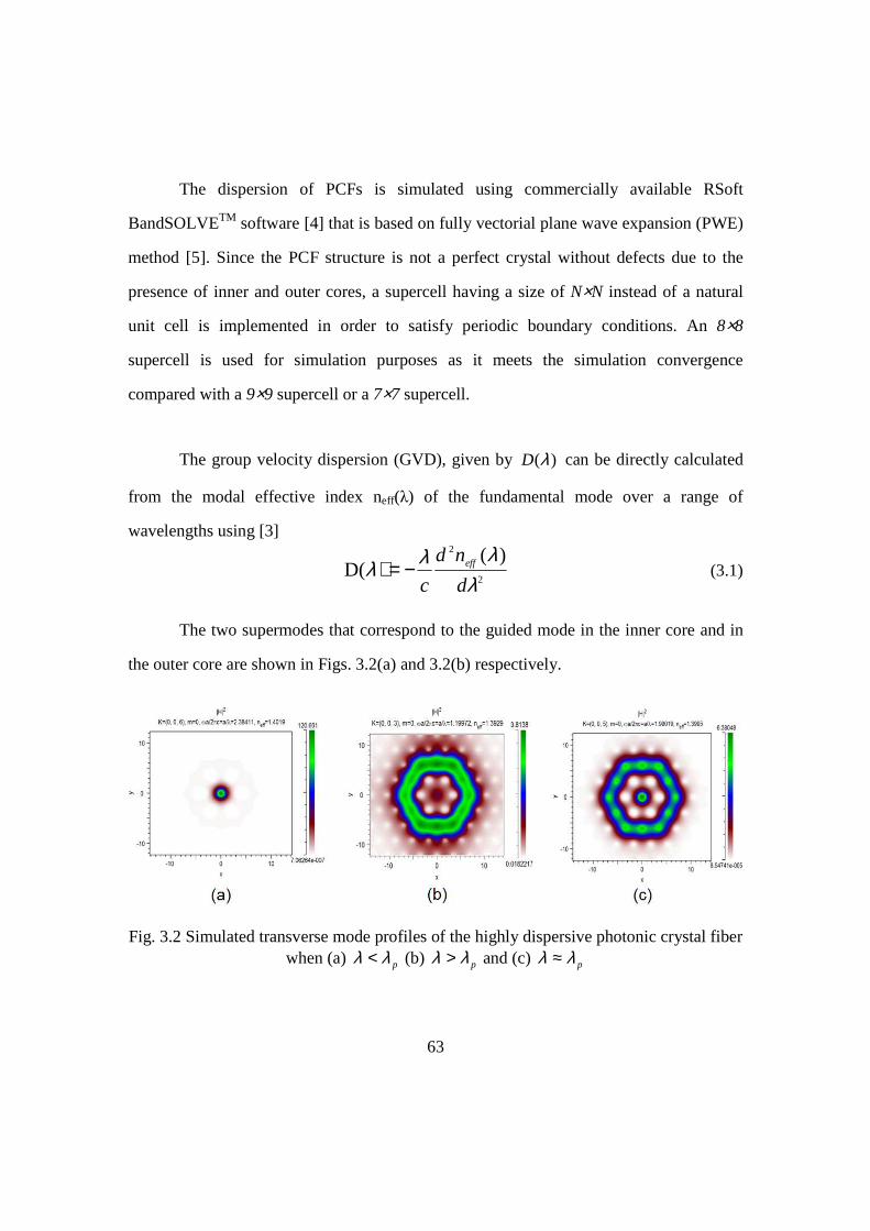
63
The dispersion of PCFs is simulated using commercially available RSoft
BandSOLVETM software [4] that is based on fully vectorial plane wave expansion (PWE)
method [5]. Since the PCF structure is not a perfect crystal without defects due to the
presence of inner and outer cores, a supercell having a size of N×N instead of a natural
unit cell is implemented in order to satisfy periodic boundary conditions. An 8×8
supercell is used for simulation purposes as it meets the simulation convergence
compared with a 9×9 supercell or a 7×7 supercell.
The group velocity dispersion (GVD), given by )(λD can be directly calculated
from the modal effective index neff(λ) of the fundamental mode over a range of
wavelengths using [3]
2
2 )(D(
λλλλ
d
nd
ceff−= ) (3.1)
The two supermodes that correspond to the guided mode in the inner core and in
the outer core are shown in Figs. 3.2(a) and 3.2(b) respectively.
Fig. 3.2 Simulated transverse mode profiles of the highly dispersive photonic crystal fiber when (a) pλλ < (b) pλλ > and (c) pλλ ≈
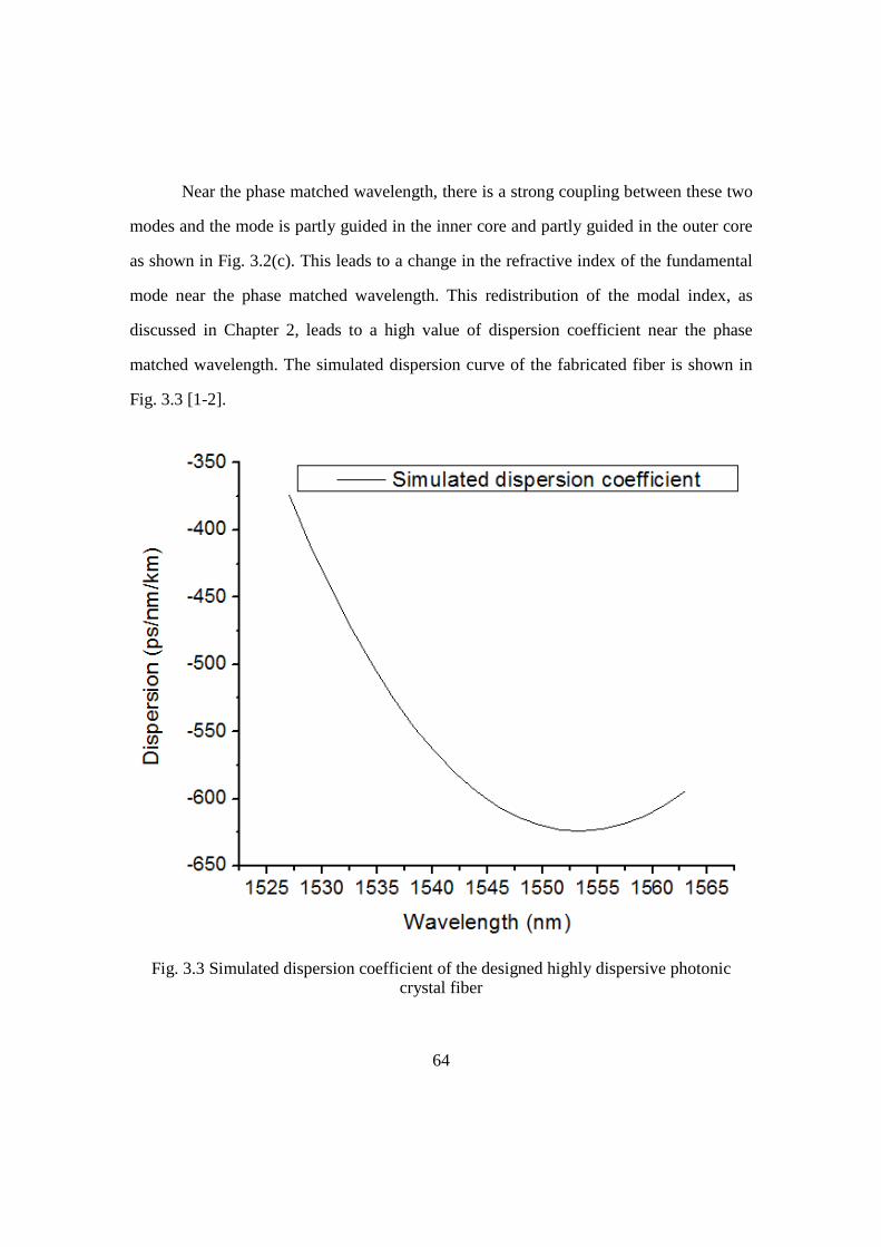
64
Near the phase matched wavelength, there is a strong coupling between these two
modes and the mode is partly guided in the inner core and partly guided in the outer core
as shown in Fig. 3.2(c). This leads to a change in the refractive index of the fundamental
mode near the phase matched wavelength. This redistribution of the modal index, as
discussed in Chapter 2, leads to a high value of dispersion coefficient near the phase
matched wavelength. The simulated dispersion curve of the fabricated fiber is shown in
Fig. 3.3 [1-2].
Fig. 3.3 Simulated dispersion coefficient of the designed highly dispersive photonic crystal fiber

65
It can be seen from the figure that very high dispersion coefficients
(exceeding kmnmps //600− ) can be achieved in this structure. This value is greater than
the dispersion coefficient of conventional single mode fibers, SMF-28
( kmnmpsDSMF //18= ) by a factor of 33, and larger by a factor of 6 compared to
dispersion compensation fibers.
3.2 Experimental characterization of true-time-delay (TTD) modules
The highly dispersive PCF is used to form a true-time-delay (TTD) module for an
X-band phased array antenna. The TTD module consists of 4 delay lines. Each delay line
consists of a length of the highly dispersive PCF connected to Lucent TrueWave SMF
non-zero dispersion shifted fiber (NZ-DSF), with dispersion coefficient kmnmps //3~
from 1530nm to 1560nm. The total length L, of each delay line is 10.5 meters, and the
lengths of PCF segments used in the 4 delay lines are 0m, 3.5m, 7m, and 10.5m
respectively [1-2]. Usually, there is a mode field diameter mismatch between the NZ-
DSF and the PCF. Therefore, at each of the ends of the PCF segments, a very short length
of ultra high numerical aperture (UHNA) fiber is spliced between the NZ-DSF and the
PCF as shown in Fig. 3.4 [6]. The UHNA also ensures selective injection of light into the
central core. The splices are protected with splice sleeves.
A wavelength of 1545nm is chosen as the central wavelength. The NZ-DSF
lengths in all the delays lines are trimmed such that the delay through each line at the
central wavelength is the same. The maximum insertion loss added due to the delay lines
is 11dB [7].

66
Fig. 3.4 Schematic representation of connection between NZ-DSF and PCF using UHNA fiber (only connections at one end of PCF are shown)
In order to obtain the chromatic dispersion of the fabricated highly dispersive
PCFs, the time delay difference (T∆ ) between optical wavelengths of 1.0±λ nm is
measured at each wavelength according to the setup explained in [8]. In order to measure
the time delay difference, the phase difference as a function of microwave frequency is
measured at optical wavelengths of ( 1.0+λ nm) and ( 1.0−λ nm). The slope of the phase
versus frequency curve gives the time delay. The dispersion coefficient (D) is calculated
using )/( LTD ⋅∆∆= λ (3.2)
where nm2.0=∆λ is the wavelength difference and L is the length of PCF (contribution
to time delay difference from NZ-DSF is negligible). The measured group velocity
dispersion curve as a function of wavelength is shown in Fig. 3.5 [9]. It can be seen from
the figure that the dispersion coefficient is as high as kmnmps //600~ − near 1550nm.
The simulated dispersion coefficient curve is also shown in the same figure.

67
Fig. 3.5 Measured dispersion coefficient of the fabricated highly dispersive photonic crystal fiber
3.2.1 TIME DELAY INTERVAL MEASUREMENT
The time delay interval between adjacent delay lines is measured using the setup
as shown in Fig. 3.6. A femtosecond laser source (FPL-01T femtosecond Erbium doped
fiber laser from Calmar Optcom Inc.) generates the optical carrier with a wavelength of
1550nm, and with an average power of 10mW. The pulse width is about 0.08ps and the
repetition rate is 19MHz. This optical signal is split to three channels using a 1-to-4
optical power splitter.

68
Fig. 3.6 Schematic of the time delay interval measurement setup using femtosecond laser source
One arm serves a trigger for the digital communication analyzer and two other
arms pass through adjacent delay lines in the TTD network. The pulse traces measured
through all the delay lines are shown in Fig. 3.7. The wavelength of 1550nm creates
different delays for the pulses through the delay lines. The pulse traces corresponding to
delays lines consisting of PCF lengths 0m, 3.5m, 7.0m, and 10.5m respectively are
numbered from 0 through 3 respectively [10]. The broad output pulses are due to the
limitation from the speed of the photodetector. It can be seen from the figure that time
delay difference values obtained between adjacent lines, say between line # 0 and line # 1
is 11.04ps, and the time delay differences between any two adjacent delay lines is

69
constant. This is a requirement for phased array antenna systems. Since using this method
only time delay differences at a wavelength of 1550nm can be obtained, another method
is used to determine the time delay differences at other wavelengths.
Fig. 3.7 Time delayed pulse traces of 4 TTD lines measured on the digital communication analyzer
3.2.2 PHASE VERSUS FREQUENCY MEASUREMENT
In order to show the true-time-delay nature and measure the time delay difference
at different wavelengths between adjacent delay lines of the module consisting of highly
dispersive PCF, a phase versus frequency measurement is performed. The schematic of
the phase versus frequency measurement setup is shown in Fig. 3.8. The microwave

70
signal in the X-band (8-12.5GHz) from an HP8510C vector network analyzer is
modulated onto an optical carrier generated by an external cavity tunable laser source
(Santec ECL-200) using a Lithium Niobate (LiNbO3) Mach-Zehnder Modulator (MZM).
The modulated carrier is split into two channels using 1-to-2 optical power splitter. One
output arm of the splitter feeds a reference TTD line consisting of 10.5m NZ-DSF, and
the other output arm is fed to the TTD line under test. After passing through the TTD
lines, the optical signals are converted back to electrical signals at the photodetector
(PD). The phase of the output electrical signal is measured with respect to the reference
arm on the network analyzer. An external tunable delay line (not shown in the schematic)
is used as an initial calibration step to equalize the phase difference between adjacent
delay lines to zero at a wavelength of 1545nm.
Fig. 3.8 Schematic of Phase versus Frequency measurement setup
At a fixed optical wavelength, the frequency of the microwave signal is changed
from 8GHz to 12GHz in steps of 0.5GHz. At each frequency, the phase difference
between the TTD line under test and the reference arm is measured using the network
analyzer and the values are noted down carefully. This procedure is repeated at different
wavelengths by tuning the laser wavelength. The measured phase versus frequency
curves for the three TTD lines are shown in Fig. 3.9 [6]. It can be seen from the figure
that the phase versus frequency plots are straight lines, which is a characteristic of true
λ
λ NETWORK ANALYZER
L
TUNABLE LASER
MZM TTD
PD RFIN
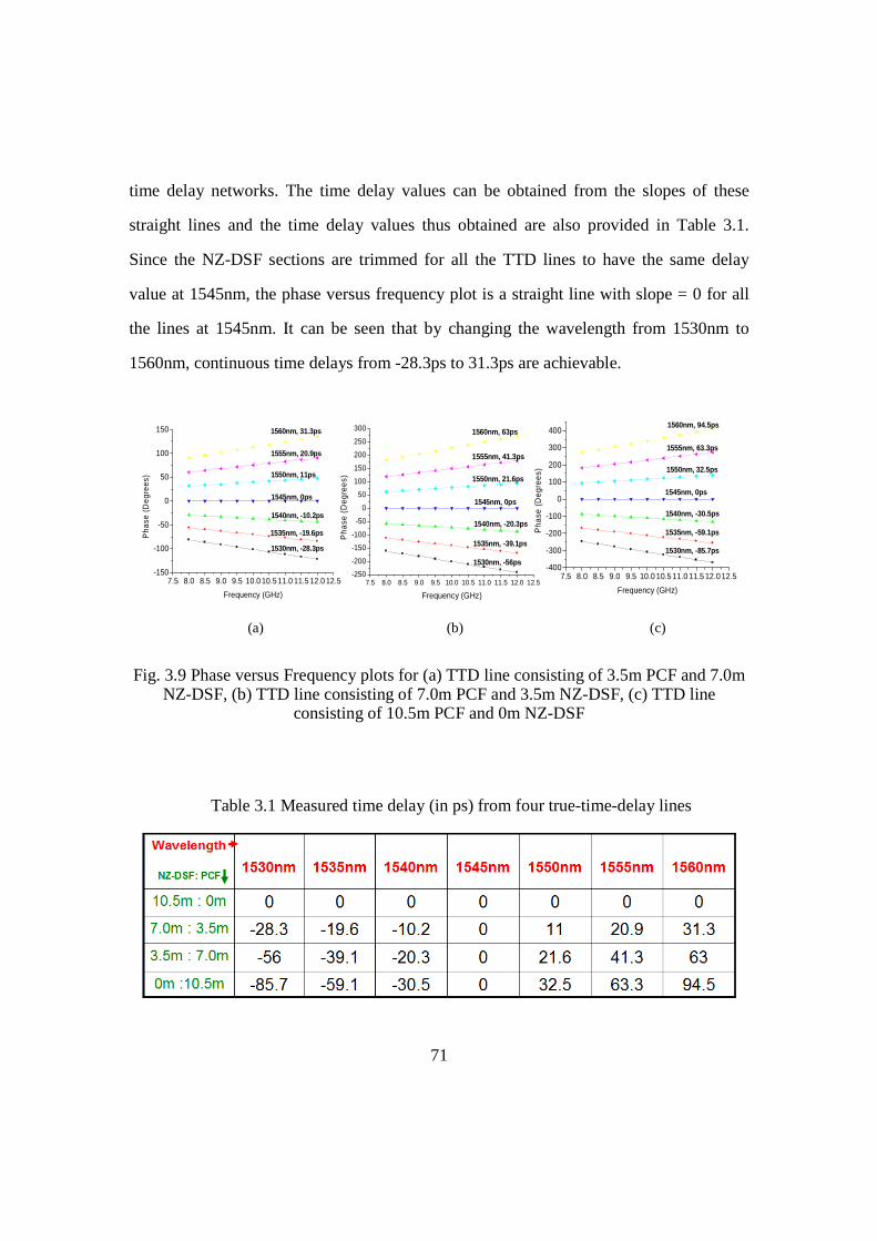
71
time delay networks. The time delay values can be obtained from the slopes of these
straight lines and the time delay values thus obtained are also provided in Table 3.1.
Since the NZ-DSF sections are trimmed for all the TTD lines to have the same delay
value at 1545nm, the phase versus frequency plot is a straight line with slope = 0 for all
the lines at 1545nm. It can be seen that by changing the wavelength from 1530nm to
1560nm, continuous time delays from -28.3ps to 31.3ps are achievable.
7.5 8.0 8.5 9.0 9.5 10.0 10.5 11.0 11.5 12.0 12.5-150
-100
-50
0
50
100
150
Pha
se (
Deg
rees
)
Frequency (GHz)
1530nm, -28.3ps
1535nm, -19.6ps
1540nm, -10.2ps
1545nm, 0ps
1550nm, 11ps
1555nm, 20.9ps
1560nm, 31.3ps
7.5 8.0 8.5 9.0 9.5 10.0 10.5 11.0 11.5 12.0 12.5-250
-200
-150
-100
-50
0
50
100
150
200
250
300
Pha
se (
Deg
rees
)
Frequency (GHz)
1560nm, 63ps
1555nm, 41.3ps
1550nm, 21.6ps
1545nm, 0ps
1540nm, -20.3ps
1535nm, -39.1ps
1530nm, -56ps
7.5 8.0 8.5 9.0 9.5 10.0 10.5 11.0 11.5 12.012.5-400
-300
-200
-100
0
100
200
300
400
Pha
se (
Deg
rees
)
Frequency (GHz)
1530nm, -85.7ps
1535nm, -59.1ps
1550nm, 32.5ps
1540nm, -30.5ps
1545nm, 0ps
1555nm, 63.3ps
1560nm, 94.5ps
(a) (b) (c)
Fig. 3.9 Phase versus Frequency plots for (a) TTD line consisting of 3.5m PCF and 7.0m NZ-DSF, (b) TTD line consisting of 7.0m PCF and 3.5m NZ-DSF, (c) TTD line
consisting of 10.5m PCF and 0m NZ-DSF
Table 3.1 Measured time delay (in ps) from four true-time-delay lines
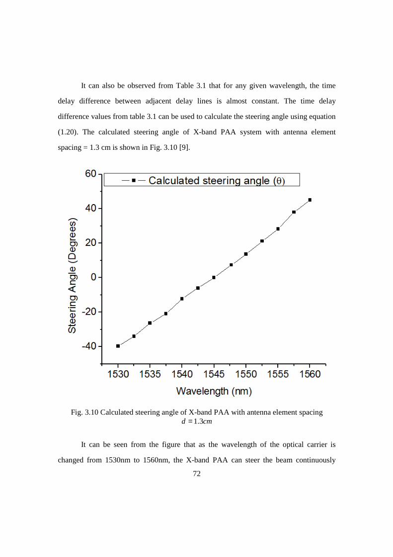
72
It can also be observed from Table 3.1 that for any given wavelength, the time
delay difference between adjacent delay lines is almost constant. The time delay
difference values from table 3.1 can be used to calculate the steering angle using equation
(1.20). The calculated steering angle of X-band PAA system with antenna element
spacing = 1.3 cm is shown in Fig. 3.10 [9].
Fig. 3.10 Calculated steering angle of X-band PAA with antenna element spacing cmd 3.1=
It can be seen from the figure that as the wavelength of the optical carrier is
changed from 1530nm to 1560nm, the X-band PAA can steer the beam continuously

73
from 041− to 046+ . This TTD network is used to demonstrate single and simultaneous
multiple RF beam transmission and reception in the subsequent chapters.
3.3 Summary
In this chapter, a practical design of a highly dispersive photonic crystal fiber was
presented. Chromatic dispersion of highly dispersive photonic crystal fiber was
theoretically simulated and experimentally measured. The dispersion of the fabricated
photonic crystal fiber, which is based on a dual concentric-core structure, was measured
to be as high as kmnmps //600− at 1550 nm. A true-time-delay network consisting of
four delay lines was formed using the fabricated highly dispersive PCF. Each delay line
in the module consisted of a length of highly dispersive PCF connected to a length of NZ-
DSF. The PCF length segment difference between adjacent delay lines in the module was
3.5m and the overall length of each delay line including PCF and NZ-DSF was 10.5m.
Time delay interval was measured using a femtosecond laser source operating at 1550nm
and a digital oscilloscope. Finally, true-time-delay nature of the TTD module was
verified by performing phase versus frequency measurements and showing linearity of
the phase-frequency plots. Time delay values at each wavelength were deduced by
calculating the slope of phase-frequency lines. The derived time delay values showed the
feasibility of steering an RF beam from -410 to +460 by tuning the wavelength from
1530nm to 1560nm for a 4-element X-band antenna array with inter-element spacing =
1.3cm.

74
3.4 References
[1] Y. Jiang, B. Howley, Z. Shi, Q. Zhou, R. T. Chen, M. Y. Chen, G. Brost, C. Lee, “Dispersion-Enhanced Photonic Crystal Fiber Array for A True-Time-Delay Structured X-band Phased Array Antenna,” IEEE. Photon. Technol. Letts. vol. 17, pp. 187-189 (2005)
[2] Y. Jiang, Z. Shi, B. Howley, X. Chen, M. Y. Chen, and R. T. Chen, “Delay Time Enhanced Photonic Crystal Fibers Array for Wireless Communications using 2-D X-band Phased Array Antennas,” Opt. Engineering. vol. 44, (2005)
[3] U. Peschel, T. Peschel, and F. Lederer, “A compact device for highly efficient dispersion compensation in fiber transmission,” Appl. Phys. Letts. vol. 67, pp. 2111-2113 (1995)
[4] RSoft Photonics CAD Suite, Version 5.1.7
[5] K. M. Ho, C. T. Chan, and C. M. Soukoulis, “Existence of a Photonic Gap in Periodic Dielectric Structures,” Phy. Rev. Letts. vol. 65, pp. 3152-3155 (1990)
[6] H. Subbaraman, M. Y. Chen, and R. T. Chen, Packaging and system demonstration of an X-band phased array antenna utilizing highly dispersive photonic crystal fiber based true-time-delay, in Proc. SPIE, vol. 7221, pp. 722107-1 (2009)
[7] H. Subbaraman, M. Y. Chen, and R. T. Chen, “Photonic dual RF beam reception of an X band phased array antenna using a photonic crystal fiber-based true-time-delay beamformer,” Appl. Opt. vol. 7, pp. 6448-6452 (2008)
[8] B. Howley, Z. Shi, Y. Jiang, and R. T. Chen, “Thermally tuned optical fiber for true time delay generation,” Opt. Laser Technol. vol. 37, pp. 29-32, (2004)
[9] H. Subbaraman, M. Y. Chen, and R. T. Chen, “Photonic Crystal Fiber-Based True-Time-Delay Beamformer for Multiple RF Beam Transmission and Reception of an X-Band Phased-Array Antenna,” J. Lightwav. Technol. vol. 26, pp. 2803-2809 (2008)
[10] M. Y. Chen, H. Subbaraman, and R. T. Chen, “Photonic Crystal Fiber Beamformer for Multiple X-band Phased-Array Antenna Transmissions,” IEEE. Photon. Technol. Letts. vol. 5, pp. 375-377 (2008)
75
Chapter 4 1x4 X-band phased array antenna subsystem for single beam transmission/reception
The PCF-TTD module described in Chapter 3 forms a continuously tunable time
delay system which can provide continuous beam steering capabilities apart from
advantages of compact size and low weight features over other optical TTD techniques
such as bulk optical TTD technique [1-5], optical non-dispersive fiber TTD technique [6],
wavelength-division-multiplexer TTD technique [7-12], holographic-grating based TTD
technique [13-14], wavelength-selective waveguide TTD technique [15], acoustic-optic
TTD technique [16-19], optical dispersion based TTD technique [20], chirped fiber
grating based TTD technique [21-22], and holographic-grating based TTD technique [23-
25] etc. In this chapter, the principle of operation and demonstration of single beam
transmission and reception of RF signals in the X-band using four true-time-delay lines
consisting of highly dispersive photonic crystal fibers and non-zero dispersion shifted
fibers will be described. By tuning the wavelength of the optical carrier, the transmission
and reception of two different RF signals will be demonstrated.
4.1 Demonstration of single RF beam transmission of PCF-TTD based X-band PAA
In this section, the principle of operation of the highly dispersive photonic crystal
fiber true-time-delay (TTD) based X-band phased array antenna system for transmitting a
single RF beam is described. Experiment is set up to transmit an RF signal with
frequency 8.4GHz to 7.4 degrees by tuning the wavelength to 1547.72nm. Similarly,
another RF signal with frequency 12GHz is transmitted to 21.2 degrees by tuning the
wavelength to 1552.52nm, thus showing the capability of the system to transmit RF

76
beams in the X-band. The experimental setup and the results are also explained in this
section.
4.1.1 PRINCIPLE OF SINGLE RF BEAM TRANSMISSION
Using the PCF based TTD module, single beam transmission can be realized by
using the schematic as shown in Fig. 4.1 [26]. A single set of PCF-TTD lines generates
the required time delay values for each element in the antenna array.
Fig. 4.1 Schematic of the Highly Dispersive PCF-TTD based PAA setup for single RF beam transmission (PCF is represented with red dots and non-zero dispersion shifted
fibers is represented with blue dots)
An external cavity tunable laser is used to provide an optical carrier wave. An RF
signal from a network analyzer is modulated onto the optical carrier wave using Lithium
Niobate Mach-Zehnder modulators (MZM). After passing through the MZM, the optical
carrier wave is amplified using an Erbium Doped Fiber Amplifier (EDFA). A 1-to-N
optical power splitter divides the amplified optical signal to N true-time-delay (TTD)
lines. As described in the previous chapter, each TTD line has consists of different
lengths of PCF and NZ-DSF segments, with overall length equal to L for each line. The
X-BAND ANTENNA
ARRAY
Y
Y
Y
Y
1:N EDFA MZM
TUNABLE LASER
TTD
PHOTODETECTOR
LNA RFIN
λ = λ0
λ < λ0
λ > λ0
L
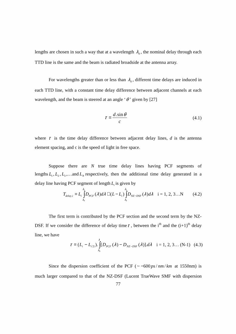
77
lengths are chosen in such a way that at a wavelength 0λ , the nominal delay through each
TTD line is the same and the beam is radiated broadside at the antenna array.
For wavelengths greater than or less than 0λ , different time delays are induced in
each TTD line, with a constant time delay difference between adjacent channels at each
wavelength, and the beam is steered at an angle ‘θ ’ given by [27]
c
d θτ sin.= (4.1)
where τ is the time delay difference between adjacent delay lines, d is the antenna
element spacing, and c is the speed of light in free space.
Suppose there are N true time delay lines having PCF segments of
lengths 1L , 2L , 3L ,…and NL respectively, then the additional time delay generated in a
delay line having PCF segment of lengthiL is given by
∫ ∫ −−+=1
0
1
0
)()()(,
λ
λ
λ
λ
λλλλ dDLLdDLT DSFNZiPCFiidelay i = 1, 2, 3…N (4.2)
The first term is contributed by the PCF section and the second term by the NZ-
DSF. If we consider the difference of delay timeτ , between the ith and the (i+1)th delay
line, we have
∫ −+ −−=λ
λ
λλλτ0
)].()([).( 1 dDDLL DSFNZPCFii i = 1, 2, 3… (N-1) (4.3)
Since the dispersion coefficient of the PCF ( kmnmps //600~ − at 1550nm) is
much larger compared to that of the NZ-DSF (Lucent TrueWave SMF with dispersion

78
coefficient kmnmps //3~ from 1530nm to 1560nm), for a fixed wavelength λ , the
difference of time delays between different channels are only determined by the lengths
of the PCF segments. Therefore, by making the lengths of the PCF an arithmetic
sequence, we can achieve equal time delay differences between adjacent TTD lines at any
given wavelength, thus, forming a wavelength-tuned TTD line. After the optical signals
pass through the TTD lines, they are converted back to electrical signals at the
photodetector bank. These electrical signals now provide the phase information for the
antenna array. Since for a fixed optical wavelength, the time delay is only related to the
lengths of PCF segments, the delay time of the each output electrical signal is controlled
continuously by tuning the optical wavelengths. Each optical wavelength creates a time
delay set corresponding to a specific steering angle as given by equation (4.1).
4.1.2 EXPERIMENTAL SETUP
Using the PCF-TTD module described in Chapter 3 in the X-band PAA setup, a
single RF beam can be transmitted and steered in space using an array antenna. The phase
control required to steer the beam is provided by wavelength tuning the TTD modules.
From the phase versus frequency measurements provided in Chapter 3, it is seen that
continuous time delay intervals from -28.3ps to 31.3ps can be achieved by tuning the
wavelength from 1530nm to 1560nm and using equation (4.1), the steering angle can be
obtained. Using the highly dispersive photonic crystal fiber TTD network, the RF beam
can be steered from -41 degrees to 46 degrees by tuning the wavelength from 1530nm to
1560nm.
In the setup, the lengths of the NZ-DSF segments in each delay line are trimmed
such that the delay difference between adjacent lines at 1545nm is zero. By tuning the

79
laser wavelength to1λ , the time delay difference (τ∆ ) from equation (1.17) can be
rewritten as
∫=−=∆ −
1
0
).(.1000
5.31
λ
λ
λλτττ dDPCFii econdspicos (4.4)
where )( 1−− ii LL in equation 1.17 is the length difference of the PCF segments between
adjacent elements (=3.5m) and )(λPCFD is the dispersion coefficient of the photonic
crystal fiber expressed in kmnmps // .
The actual experimental setup used for demonstrating single RF beam
transmission in Fig 4.2(a) [26]. Optical carrier from an external cavity tunable laser
source (Santec ECL-200) is modulated with an X-band RF signal generated by HP 8510C
vector network analyzer, using a high speed Lithium Niobate (LiNbO3) modulator. The
modulated optical signal is amplified using an Erbium-doped fiber amplifier (EDFA)
which provides a maximum output power of 13dBm. The amplified signal is split into 4
channels using a 1-to-4 optical power splitter and distributed to the four TTD lines. The
total length L, of each delay line is 10.5 meters, and the lengths of PCF segments used in
the 4 delay lines are 0m, 3.5m, 7m, and 10.5m respectively. The 4 delay lines are shown
in Fig. 4.2(b). The compositions of the lines are also shown in the inset [26].
The lengths are chosen such that at a wavelength of 1545nm, the nominal delay
through each TTD line is the same. This implies that at 1545nm, the RF signal is radiated
broadside at the X-band (8-12.5GHz) antenna array. At any other wavelength, the beam
is steered to a different direction depending on the time delay differences between

80
(c)

81
Fig. 4.2 Experimental setup of the PAA in transmitting mode (a) Overall setup along with an expanded view of the antenna array is shown. (b) The four TTD lines are shown. The
inset shows the composition of each line. (c) The receiving horn antenna and the microwave spectrum analyzer are shown
adjacent delay lines. A photodetector bank converts the optical signals into electrical
signals. Electrical tunable delay lines are used to fine tune the delays such that the delay
through all TTD lines are equal at a wavelength of 1545nm. These signals are then
amplified by an X-band low noise amplifier (LNA). After amplification, the electrical
signals are fed to the center 4 adjacent elements of an antenna array, which has an
element spacing of 1.3cm. An enlarged picture of the antenna array is also shown in the
inset of Fig. 4.2(a). The far field radiation pattern of the X-band PAA is measured by
fixing the antenna array on an accurate positioner and measuring the received power by a
fixed standard horn antenna connected to a microwave spectrum analyzer (MSA). The
receiving horn antenna and the microwave spectrum analyzer are shown in Fig. 4.2(c).
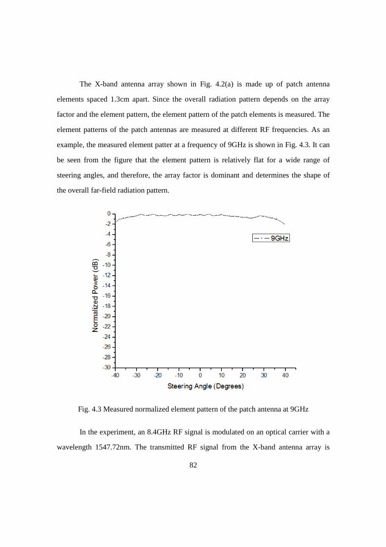
82
The X-band antenna array shown in Fig. 4.2(a) is made up of patch antenna
elements spaced 1.3cm apart. Since the overall radiation pattern depends on the array
factor and the element pattern, the element pattern of the patch elements is measured. The
element patterns of the patch antennas are measured at different RF frequencies. As an
example, the measured element patter at a frequency of 9GHz is shown in Fig. 4.3. It can
be seen from the figure that the element pattern is relatively flat for a wide range of
steering angles, and therefore, the array factor is dominant and determines the shape of
the overall far-field radiation pattern.
Fig. 4.3 Measured normalized element pattern of the patch antenna at 9GHz
In the experiment, an 8.4GHz RF signal is modulated on an optical carrier with a
wavelength 1547.72nm. The transmitted RF signal from the X-band antenna array is

83
received by the receiving horn antenna, which is placed at a distance greater than the far-
field distance (~ 4 meters). The antenna head is rotated on a precision micro-rotation
stage and the received power at the horn antenna is measured as a function of the steering
angle on the microwave spectrum analyzer. Similarly, the experiment is also performed
for a 12GHz signal using an optical carrier wavelength of 1552.52nm.
4.1.3 RESULTS AND DISCUSSION
Figs. 4.4(a) and 4.4(b) show the measured far-field radiation pattern of the
8.4GHz signal (curve marked as solid triangles) and the 12GHz signal (curve marked as
solid squares) at optical carrier wavelengths of 1547.72nm and 1552.52nm respectively
[26].

84
Fig. 4.4 Simulated and measured far field patterns for (a) RF signal with frequency = 8.4GHz at a wavelength of 1547.72nm. (b) RF signal with frequency = 12GHz at a
wavelength of 1552.52nm
The simulated far field radiation patterns are shown in both the figures as
continuous solid curves. It can be seen from the figures that the maximum received
powers occur at 7.4 degrees and 21.2 degrees for 8.4GHz and 12GHz respectively. These
angles are also shown as data points on Fig. 3.10. It can also be seen from the figures that
the measured patterns agree well with the simulated results, thus showing the capability
of single beam transmitting capability of the system. Therefore, by tuning the optical
wavelength of the carrier, the RF beam can be steered in space.
85
In order to bean squint-free nature of the PCF-TTD network, far field radiation
patterns of two RF signals at 8.4GHz and 10.3GHz respectively are measured by using an
optical carrier wavelength of 1523nm and the measured far-field radiation patterns are
shown in Fig. 4.5. It can be seen from the figure that the maximum transmitted power for
both 8.4GHz (curve marked with solid circles) and 10.3GHz (curve marked with solid
triangles) occur at -23 degrees. The measured and simulated results agree well with each
other. This result shows that the PCF-TTD has a frequency independent steering angle
capability and thus has a beam squint-free operation.
Fig. 4.5 Beam squint-free demonstration of the PCF-TTD based phased array antenna system
86
4.2 Demonstration of single RF beam reception of PCF-TTD based X-band PAA
The PCF-TTD based PAA architecture can also be used to receive an incoming
RF signal and determine the angle of arrival accurately. In this section, the principle of
operation of the highly dispersive photonic crystal fiber true-time-delay (TTD) based X-
band phased array antenna system for receiving a single RF beam is described.
Experiment is set up to receive an RF signal with frequency 8.4GHz from -7.4 degrees by
tuning the wavelength to 1547.72nm. Similarly, another RF signal with frequency 12GHz
is received from -21.2 degrees by tuning the wavelength to 1552.52nm, thus showing the
capability of the system to receive RF beams in the X-band. The experimental setup and
the results are also explained in this section.
4.2.1 PRINCIPLE OF SINGLE RF BEAM RECEPTION
Since the incoming RF beam travels a different path length in order to reach each
of the two antenna elements, a phase difference between the two signals is created. These
received RF signals from the antenna elements are amplified using LNAs and modulated
onto the optical carrier. The optical signal feeding each MZM is obtained by splitting the
optical carrier from a tunable laser source using a 1-to-N optical power splitter.
Depending on the wavelength of the optical carrier, the TTD lines also induce additional
phase shifts to the original signals. Therefore, if the additional phase shift has a sign
opposite to the once created by the incoming beams, then the two signals coming out of
the TTD lines will be in phase and they will add up at the N-to-1 power combiner and
produce a maximum power on the microwave spectrum analyzer. Thus, if the incoming
beam is arriving from a direction ‘θ ’, then the optical wavelength that can cancel the
phase difference is the one that would direct a beam at an angle of ‘-θ ’ in the

87
transmitting mode. Therefore, there is a peak on the plot of the combined power at the
photodetector versus wavelength. The wavelength at which the peak occurs can be used
in conjunction with steering angle data as shown in Fig. 3.10 to accurately determine the
angle of arrival.
Using the highly dispersive photonic crystal fiber TTD network, the incoming RF
beam can be detected from 41 degrees to -46 degrees by tuning the wavelength from
1530nm to 1560nm and its angle of arrival can be determined accurately.
4.2.2 EXPERIMENTAL SETUP
The beam receiving and angle of arrival determining capability of the PCF-TTD
based PAA system can be demonstrated by slightly modifying the single beam
transmission setup. A schematic of the setup used to detect and determine the angle of
arrival of the incoming RF beam is shown in Fig. 4.6 [26]. In the case of single beam
transmission, only one modulator is required to modulate the RF signal onto the optical
carrier. In the case of receiving mode operation however, since each element receives the
RF signal, one modulator per antenna element is required. Since we are limited by the
available hardware in the laboratory, the receiving mode experiment is performed using
center two adjacent antenna elements.
The RF signal impinging on the antenna array is generated by a HP 8620C sweep
oscillator. A horn antenna is used to transmit the signal towards the X-band antenna
array. The horn antenna is placed at an angle with respect to the antenna array. The
incoming signal is received by the two adjacent center antenna elements on the lower line
of X-band antenna array shown in the inset of Fig. 4.2(a).
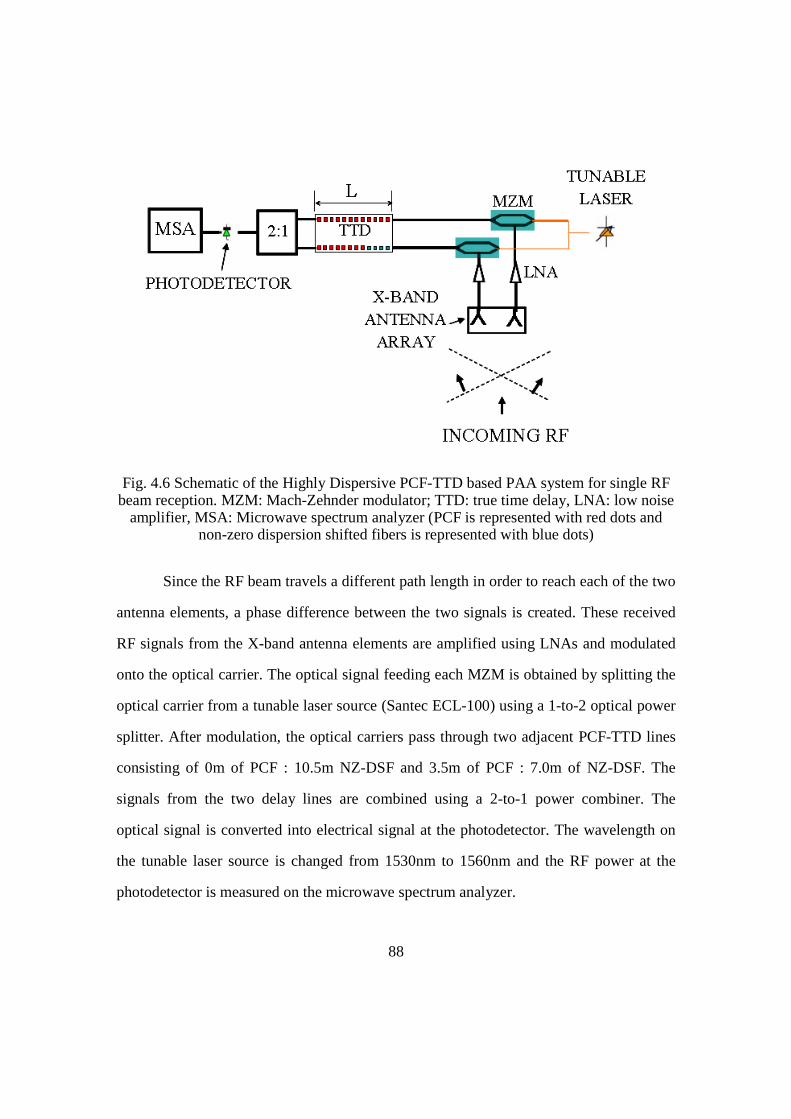
88
Fig. 4.6 Schematic of the Highly Dispersive PCF-TTD based PAA system for single RF beam reception. MZM: Mach-Zehnder modulator; TTD: true time delay, LNA: low noise
amplifier, MSA: Microwave spectrum analyzer (PCF is represented with red dots and non-zero dispersion shifted fibers is represented with blue dots)
Since the RF beam travels a different path length in order to reach each of the two
antenna elements, a phase difference between the two signals is created. These received
RF signals from the X-band antenna elements are amplified using LNAs and modulated
onto the optical carrier. The optical signal feeding each MZM is obtained by splitting the
optical carrier from a tunable laser source (Santec ECL-100) using a 1-to-2 optical power
splitter. After modulation, the optical carriers pass through two adjacent PCF-TTD lines
consisting of 0m of PCF : 10.5m NZ-DSF and 3.5m of PCF : 7.0m of NZ-DSF. The
signals from the two delay lines are combined using a 2-to-1 power combiner. The
optical signal is converted into electrical signal at the photodetector. The wavelength on
the tunable laser source is changed from 1530nm to 1560nm and the RF power at the
photodetector is measured on the microwave spectrum analyzer.
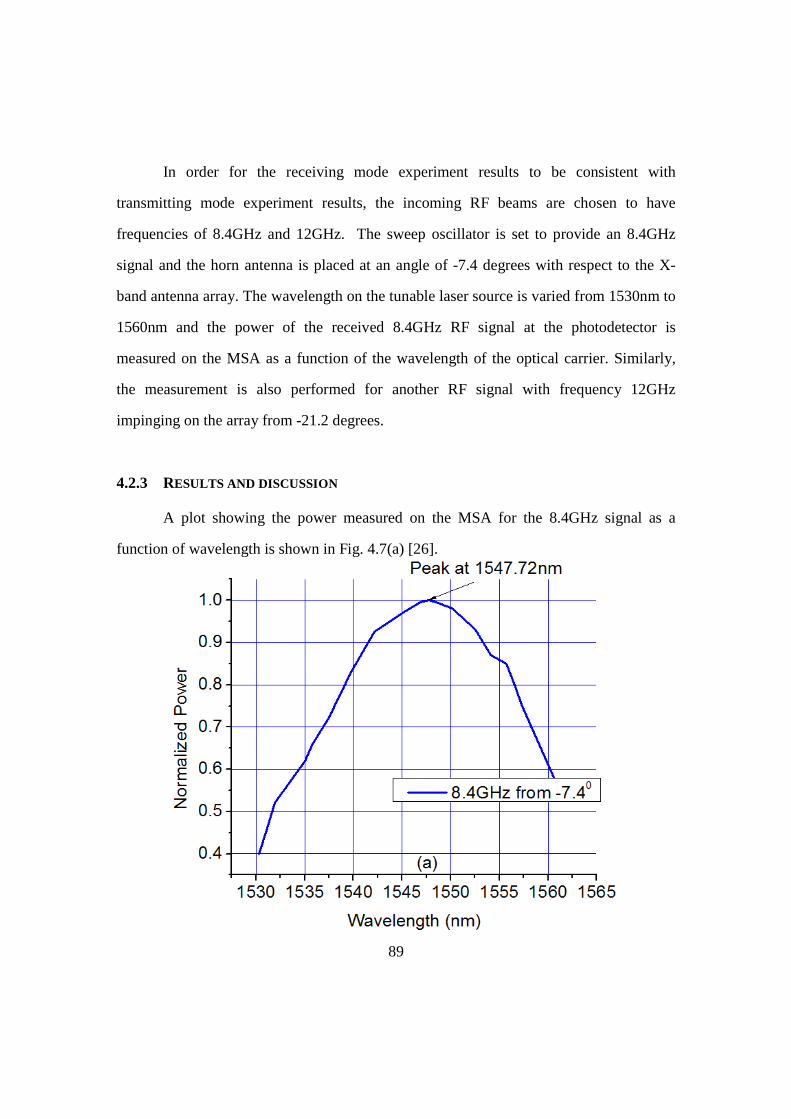
89
In order for the receiving mode experiment results to be consistent with
transmitting mode experiment results, the incoming RF beams are chosen to have
frequencies of 8.4GHz and 12GHz. The sweep oscillator is set to provide an 8.4GHz
signal and the horn antenna is placed at an angle of -7.4 degrees with respect to the X-
band antenna array. The wavelength on the tunable laser source is varied from 1530nm to
1560nm and the power of the received 8.4GHz RF signal at the photodetector is
measured on the MSA as a function of the wavelength of the optical carrier. Similarly,
the measurement is also performed for another RF signal with frequency 12GHz
impinging on the array from -21.2 degrees.
4.2.3 RESULTS AND DISCUSSION
A plot showing the power measured on the MSA for the 8.4GHz signal as a
function of wavelength is shown in Fig. 4.7(a) [26].

90
Fig. 4.7 Measured received power versus wavelength for (a) 8.4GHz RF signal impinging on the antenna array from -7.40 (b) 12GHz RF signal impinging on the antenna array
from -21.20
It can be seen from the figure that a peak in the power at the photodetector is
obtained at a wavelength of 1547.72nm. The wavelength at which the peak occurs can be
used in conjunction with steering angle data as shown in Fig. 3.10 to accurately
determine the angle of arrival. The peak wavelength in Fig. 4.7(a) corresponds to a
complementary angle of 7.4 degrees in the transmitting mode. Similarly, for the 12GHz
signal placed at an angle of -21.2 degrees with respect to the antenna array normal, the
plot of the measured power as a function of wavelength is shown in Fig. 4.7(b). It can be
seen from the figure that a peak in the power at the photodetector is obtained at a
wavelength of 1552.52nm. This corresponds to a complementary angle of 21.2 degrees in
91
the transmitting mode. These results prove the feasibility of using the PCF-TTD based X-
band PAA in the receiving mode.
4.3 Summary
In this chapter, the principle of operation and demonstration of single beam
transmission and reception of PCF-TTD based X-band PAA system was explained. By
tuning the optical wavelength, transmission of two RF signals with frequencies 8.4GHz
and 12GHz to 7.4 degrees and 21.2 degrees respectively was observed by tuning the
wavelengths respectively to 1547.72nm and 1552.52nm. Single RF beam receiving
capability was demonstrated by receiving two RF signals with frequencies 8.4GHz and
12GHz from -7.4 degrees and -21.2 degrees respectively by detecting peak in the
received power by tuning the optical wavelengths to 1547.72nm and 1552.52nm
respectively. Thus, the capability of the PAA system to transmit and receive single RF
beams was successfully demonstrated.
4.4 References
[1] D. Dolfi, J. P. Huignard, and M. Baril, “Optically controlled true-time delays for phased array antenna,” Proc. SPIE. vol. 1102, pp. 152 (1989)
[2] D. Dolfi, F. Michel-Gabriel, S. Bann, and J. P. Huignard, “Two-dimensional optical architecture for true-time-delay beam forming in a phased-array antenna,” Opt. Letts. vol. 16, pp. 255-257 (1991)
[3] D. Dolfi, P. Joffre, J. Antoine, J. P. Huignard, D. Philippet, and P. Granger, “Experimental demonstration of a phased-array antenna optically controlled with phase and time delays,” Appl. Opt. vol. 35, pp. 5293-5300 (1996)
[4] N. A. Riza, “Transmit/receive time-delay beam-forming optical architecture for phased-array antennas,” Appl. Opt. vol. 30, pp. 4594-4595 (1991)

92
[5] N. A. Riza, “Liquid crystal-based optical time delay control system for wideband phased arrays,” Proc. SPIE. vol. 1790, pp. 171-183 (1992)
[6] A. M. Levine, “Use of fiber optic frequency and phase determining element in radar,” in Proceedings of the 33rd Annual Symposium on Frequency Control, IEEE, 436-443 (1979)
[7] P. M. Freitag and S. R. Forrest, “A coherent optically controlled phased array antenna system,” IEEE. Microwav. Guided. Wav. Letts. vol. 3, pp. 293-295 (1993)
[8] L. Xu, R. Taylor, and S. R. Forrest, “True-time delay phased array antenna feed system based on optical heterodyne techniques,” IEEE. Photon. Technol. Letts. vol. 8, pp. 160-162 (1996)
[9] D. K. T. Tong, and M. C. Wu, “A novel multiwavelength optically controlled phased array antenna with a programmable dispersion matrix,” IEEE. Photon. Technol. Letts. vol. 8, pp. 812-814 (1996)
[10] P. Goutzoulis and D. K. Davies, “Hardware-compressive 2-D fiber-optic delay line architecture for time steering of phased-array antennas,” Appl. Opt. vol. 29, pp. 5353-5359 (1990)
[11] P. Goutzoulis and D. K. Davies, “All-optical hardware-compressive wavelength multiplexed fiber optic architecture for true-time delay steering of 2-D phased array antenna,” Proc. SPIE. vol. 1703, pp. 604-614 (1992)
[12] P. Goutzoulis and D. K. Davies, J. Zomp, P. Hrycak, and A. Johnson, “Development and field demonstration of a hardware-compressive fiber-optic true time delay steering system for phased array antennas,” Appl. Opt. vol. 33, pp. 8173-8185 (1994)
[13] Y. Chen and R. T. Chen, “A fully packaged true time delay module for a K-band phased array antenna system demonstration,” IEEE. Photon. Technol. Letts. vol. 14, pp. 1175 – 1177 (2002)
[14] Z. Fu and R. T. Chen, “Highly packing density optical true-time delay lines for phased array antenna applications,” Recent Research Developments Series, pp. 1, Dec. 1998
[15] S. Yegnanarayanan, P. D. Trinh, and B. Jalali, “Recirculating photonic filter: a wavelength-selective time delay for phased array antennas and wavelength code division multiple access,” Opt. Letts. vol. 21, pp. 740-742 (1996)
[16] W. D. Jemison and P. R. Herczfeld, “Acousto-optically controlled true-time delay,” IEEE. Microwav. Guided Wav. Letts. vol. 3, pp. 72-75 (1993)

93
[17] L. H. Gesell, R. E. Feinleib, J. L. Lafuse, and T. M. Turpin, “Acousto-optic control of time delays for array beam steering,” Proc. SPIE. vol. 2155, 194 (1994)
[18] E. N. Toughlian and H. Zmuda, “A photonic variable RF delay line for phased array antennas,” IEEE. J. Lightwav. Technol. vol. 8, pp. 1824-1828 (1990)
[19] E. H. Monsay, K. C. Baldwin, and M. J. Caucuitto, “Photonic true-time delay for high-frequency phased array systems,” IEEE. Photon. Technol. Letts. vol. 6, pp. 118-120 (1994)
[20] R. Soref, “Optical dispersion technique for time-delay beam steering,” Appl. Opt. vol. 31, pp. 7395-7397 (1992)
[21] J. L. Cruz, B. Ortega, M. V. Andres, B. Gimeno, D. Pastor, J. Capmany, and L. Dong, “Chirped fiber gratings for phased array antenna,” Electron. Letts. vol. 33, pp. 545-546 (1997)
[22] J. L. Corral, J. Marti, S. Regidor, J. M. Fuster, R. Laming, and M. J. Cole, “Continuously variable true time-delay optical feeder for phased-array antenna employing chirped fiber gratings,” IEEE. Trans. Microwav. Theory. Techniq. vol. 45, pp. 1531-1536 (1997)
[23] Z. Shi, Y. Jiang, B. Howley, Y. Chen, F. Zhao, and R. T. Chen, "Continuously delay time tunable-waveguide hologram module for X-band phased-array antenna,” IEEE. Photon. Technol. Letts. vol. 15, pp. 972-974 (2003)
[24] Z. Shi, L. Gu, B. Howley, Y. Jiang, Q. Zhou, R. T. Chen, M. Y. Chen, X. Wang, H. R. Fetterman, and G. Brost, “True-time-delay modules based on single tunable laser in conjunction with waveguide-hologram for phased-array antenna,” Opt. Engineering. vol. 44, 084301, (2005)
[25] X. Chen, Z. Shi, L. Gu, B. Howley, Y. Jiang, and R. T. Chen, “Miniaturized Delay time-enhanced Photopolymer Waveguide Hologram Module for Phased-Array Antenna,” IEEE. Photon. Technol. Letts. vol. 17, pp. 2182-2184, (2005)
[26] H. Subbaraman, M. Y. Chen, and R. T. Chen, “Packaging and system demonstration of an X-band phased array antenna utilizing highly dispersive photonic crystal fiber based true-time-delay,” in Proc. SPIE, vol. 7221, pp. 722107-1 (2009)
[27] W. Ng, A. A. Walston, G. L. Tangonan, J. J. Lee, I. L. Newberg, and N. Bernstein, “The first demonstration of an optically steered microwave phased array antenna using true-time-delay,” IEEE. J. Lightwav. Technol. vol. 9, pp. 1124- 1131 (1991)

94
Chapter 5 Simultaneous multiple-beam transmission and reception of a PCF TTD-based X-band phased array antenna
In the previous chapter, the results of the demonstration of single beam
transmission and reception of RF beams using the photonic crystal fiber true-time-delay
based X-band phased array antenna system was presented. In this chapter, application of
the TTD network will be extended to show simultaneous multiple RF beam transmission
and reception capability of the X-band phased antenna array utilizing PCF-TTD for the
first time. The principle of simultaneous multiple RF beam transmission and reception
will be described and experimental results of simultaneous dual RF beam transmission
and reception capability of the PAA system will be demonstrated.
5.1 Principle of simultaneous multiple RF beam transmission
Using the PCF based TTD module, multiple-beam transmission can be realized by
using the scheme as shown in Fig. 5.1 [1, 2]. A general system is shown in which a
multiple number (M) of RF signals are transmitted simultaneously using an X-band
antenna array having N elements.
External cavity tunable lasers are used to generate a multiple number of optical
carrier waves with wavelengths 1λ to Mλ . RF signals with different frequencies are
modulated onto these optical carrier waves using Lithium Niobate Mach-Zehnder
modulators (MZMs). After passing through the MZMs, the optical carrier waves are
combined together using an M-to-1 power combiner and these optical signals are
amplified using an Erbium Doped Fiber Amplifier (EDFA). A 1-to-N optical power
splitter divides the amplified optical signal to N true-time-delay (TTD) lines. Each TTD

95
line has consists of different lengths of PCF and NZ-DSF segments, with overall length
equal to L for each line. As described earlier, the lengths are chosen in such a way that at
a wavelength 0λ , the nominal delay through each TTD line is the same and the beam is
radiated broadside at the antenna array. Transition to multiple beam capability from
single beam setup is straightforward as only a single set of PCF-TTD lines generates the
required time delay values for each element in the antenna array and for all multiple
beams.
Fig. 5.1 Schematic setup for simultaneous transmission of multiple beams, EOM: electro-optic modulator, EDFA: Erbium doped fiber amplifier, TTD: true-time-delay. The
cross sectional schematic view of the PCF is also shown
From the previous chapter we know that the additional time delay generated in a
delay line having PCF segment of lengthiL by changing the wavelength from 0λ to 1λ is
given by

96
∫ ∫ −−+=1
0
1
0
)()()(,
λ
λ
λ
λ
λλλλ dDLLdDLT DSFNZiPCFiidelay i = 1, 2, 3…N (5.1)
where, the first term is contributed by the PCF section and the second term by the NZ-
DSF and the time delay difference (τ ), between the ith and the (i+1)th delay line is given
by
∫ −+ −−=λ
λ
λλλτ0
)].()([).( 1 dDDLL DSFNZPCFii i = 1, 2, 3…(N-1) (5.2)
We see from equation (5.2) that the time delay difference is independent of the RF
frequency. The steering angle given by
×= −
d
c τθ 1sin is also independent of the RF
frequency used [3]. Therefore, by modulating one RF signal on one optical carrier, the
different RF beams can be independently and simultaneously transmitted and steered.
Therefore, in order to simultaneously transmit N RF beams, N electro-optic modulators
and N tunable laser sources need to be used. After the optical signals pass through the
TTD lines, they are converted back to electrical signals at the photodetector bank. Since
for a fixed optical wavelength, the time delay is only related to the lengths of PCF
segments, the delay time of the each output electrical signal is controlled continuously by
tuning the optical wavelengths. Each optical wavelength creates a time delay set
corresponding to a specific steering angle as given by equation (5.1). Since different RF
signals are modulated on separate optical carriers, by injecting these multiple
wavelengths simultaneously, one can generate equivalent number of independently
steered RF far field patterns at the same time due to the squint-free nature of the TTD
lines.
97
5.2 Demonstration of simultaneous multiple beam transmission of a PCF-TTD based X-band PAA
Due to the limitation on the availability of hardware in the laboratory, a
simultaneous dual RF beam transmission experiment is performed. This section describes
the experimental setup and provides the results of simultaneous dual RF beam
transmission using PCF-TTD based X-band PAA system for the first time.
5.2.1 EXPERIMENTAL SETUP
The experimental setup used for the demonstration of simultaneous dual-beam
steering is shown in Fig. 5.2 [2]. Two tunable laser sources (Santec ECL-100) are used to
generate two optical carriers with different wavelengths. The tunable lasers have an
output power of 8dBm. An HP8620C sweep oscillator and an HP8510C network analyzer
generate two RF signals with frequencies 8.4GHz and 12GHz respectively, which are
independently modulated onto the two optical carriers using two high speed LiNbO3
modulators. A maximum of 7dB loss is encountered after passing through the modulator.
The optical signals are first combined through an optical combiner and amplified using
an EDFA. The EDFA has a maximum output of 13dBm. The amplified signal is split into
4 channels using a 1:4 optical power splitter and distributed to the four TTD lines. The
power splitting creates fan-out loss of 6dB for each delay line path. The maximum
insertion loss added due to the delay lines is 11dB. The photodetector bank converts the
optical signals into electrical signals. Tunable delay lines are used to fine tune the delays
as an initial calibration step such that the delay through the TTD lines are equal at
1545nm. These electrical signals are then amplified by the X-band low noise amplifiers
(LNA) that have a gain of 35dB. After amplification, the electrical signals are fed to a 4-
element X-band antenna array, which has an element spacing of 1.3cm.
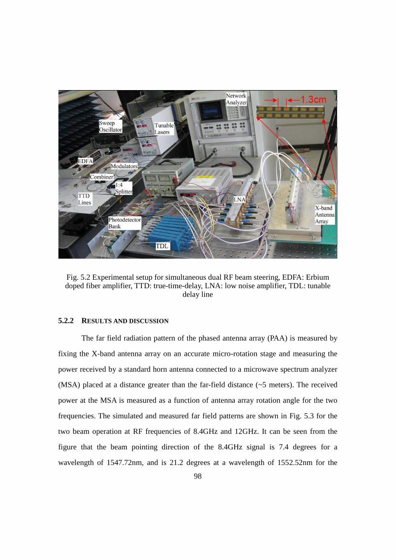
98
Fig. 5.2 Experimental setup for simultaneous dual RF beam steering, EDFA: Erbium doped fiber amplifier, TTD: true-time-delay, LNA: low noise amplifier, TDL: tunable
delay line
5.2.2 RESULTS AND DISCUSSION
The far field radiation pattern of the phased antenna array (PAA) is measured by
fixing the X-band antenna array on an accurate micro-rotation stage and measuring the
power received by a standard horn antenna connected to a microwave spectrum analyzer
(MSA) placed at a distance greater than the far-field distance (~5 meters). The received
power at the MSA is measured as a function of antenna array rotation angle for the two
frequencies. The simulated and measured far field patterns are shown in Fig. 5.3 for the
two beam operation at RF frequencies of 8.4GHz and 12GHz. It can be seen from the
figure that the beam pointing direction of the 8.4GHz signal is 7.4 degrees for a
wavelength of 1547.72nm, and is 21.2 degrees at a wavelength of 1552.52nm for the
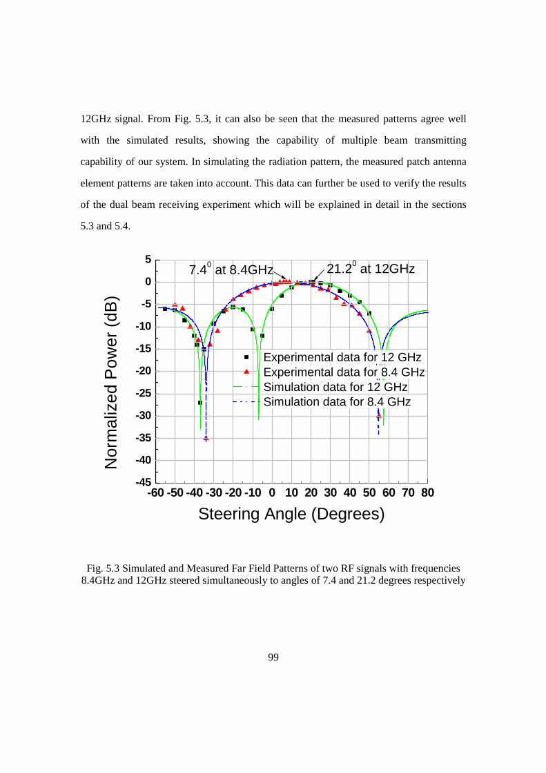
99
12GHz signal. From Fig. 5.3, it can also be seen that the measured patterns agree well
with the simulated results, showing the capability of multiple beam transmitting
capability of our system. In simulating the radiation pattern, the measured patch antenna
element patterns are taken into account. This data can further be used to verify the results
of the dual beam receiving experiment which will be explained in detail in the sections
5.3 and 5.4.
-60 -50 -40 -30 -20 -10 0 10 20 30 40 50 60 70 80-45
-40
-35
-30
-25
-20
-15
-10
-5
0
521.20 at 12GHz7.40 at 8.4GHz
Nor
mal
ized
Pow
er (
dB)
Steering Angle (Degrees)
Experimental data for 12 GHz Experimental data for 8.4 GHz Simulation data for 12 GHz Simulation data for 8.4 GHz
Fig. 5.3 Simulated and Measured Far Field Patterns of two RF signals with frequencies 8.4GHz and 12GHz steered simultaneously to angles of 7.4 and 21.2 degrees respectively
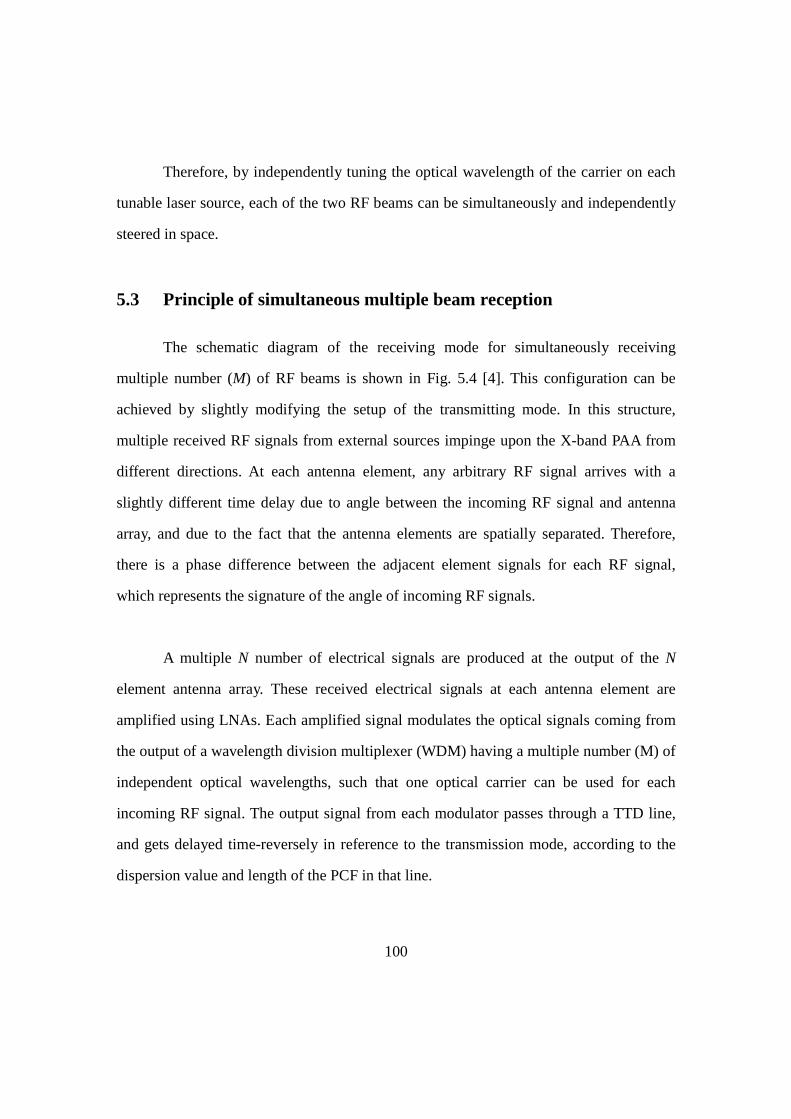
100
Therefore, by independently tuning the optical wavelength of the carrier on each
tunable laser source, each of the two RF beams can be simultaneously and independently
steered in space.
5.3 Principle of simultaneous multiple beam reception
The schematic diagram of the receiving mode for simultaneously receiving
multiple number (M) of RF beams is shown in Fig. 5.4 [4]. This configuration can be
achieved by slightly modifying the setup of the transmitting mode. In this structure,
multiple received RF signals from external sources impinge upon the X-band PAA from
different directions. At each antenna element, any arbitrary RF signal arrives with a
slightly different time delay due to angle between the incoming RF signal and antenna
array, and due to the fact that the antenna elements are spatially separated. Therefore,
there is a phase difference between the adjacent element signals for each RF signal,
which represents the signature of the angle of incoming RF signals.
A multiple N number of electrical signals are produced at the output of the N
element antenna array. These received electrical signals at each antenna element are
amplified using LNAs. Each amplified signal modulates the optical signals coming from
the output of a wavelength division multiplexer (WDM) having a multiple number (M) of
independent optical wavelengths, such that one optical carrier can be used for each
incoming RF signal. The output signal from each modulator passes through a TTD line,
and gets delayed time-reversely in reference to the transmission mode, according to the
dispersion value and length of the PCF in that line.
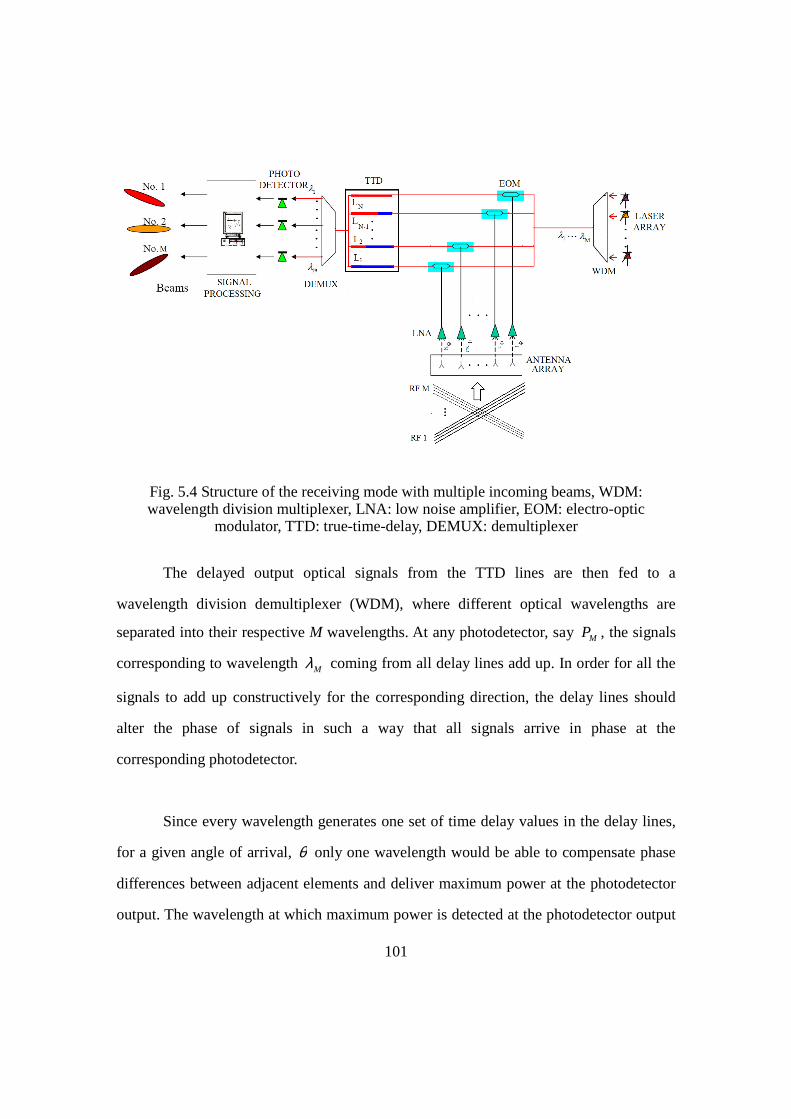
101
Fig. 5.4 Structure of the receiving mode with multiple incoming beams, WDM: wavelength division multiplexer, LNA: low noise amplifier, EOM: electro-optic
modulator, TTD: true-time-delay, DEMUX: demultiplexer
The delayed output optical signals from the TTD lines are then fed to a
wavelength division demultiplexer (WDM), where different optical wavelengths are
separated into their respective M wavelengths. At any photodetector, say MP , the signals
corresponding to wavelength Mλ coming from all delay lines add up. In order for all the
signals to add up constructively for the corresponding direction, the delay lines should
alter the phase of signals in such a way that all signals arrive in phase at the
corresponding photodetector.
Since every wavelength generates one set of time delay values in the delay lines,
for a given angle of arrival, θ only one wavelength would be able to compensate phase
differences between adjacent elements and deliver maximum power at the photodetector
output. The wavelength at which maximum power is detected at the photodetector output
102
corresponds to one angle of arrival. The angle of arrival can thus be determined for any
RF signal of interest due to the squint-free nature of the true-time delay lines.
5.4 Demonstration of simultaneous multiple beam reception of a PCF-TTD based X-band PAA
As was in the case of simultaneous dual RF beam transmission, hardware
limitation in the laboratory limits the demonstration of simultaneous multiple RF beam
reception to two beams. An experiment is performed to simultaneously receive and
determine the angle of arrival of two incoming RF signals. This section describes the
experimental setup and provides the results of simultaneous dual RF beam reception
using PCF-TTD based X-band PAA system for the first time.
5.4.1 EXPERIMENTAL SETUP
An experiment is performed in order to receive two RF beams simultaneously and
determine the angle of arrival of each incoming signal. The experimental setup used in
the demonstration is shown in Fig. 5.5 [4]. A schematic of the simultaneous dual beam
setup is also shown for clarity.
In order to perform the experiment, center two adjacent elements of the X-band
antenna array, two LiNbO3 modulators and two adjacent delay lines in the setup are used.
The 2 delay lines consist of 0 meters of PCF : 10.5 meters of NZ-DSF and 3.5 meters of
PCF : 7 meters of NZ-DSF respectively. As discussed previously, the lengths of the NZ-
DSF sections are trimmed such that at 1545nm, the delays in each of the delay lines are
equal. That is, for an RF signal incident normally on the antenna array, modulating a
103
wavelength of 1545nm, the signal detected at the photodetector will be a maximum.
Therefore, different angle of arrival of RF signal will require a different wavelength to
equalize the phase difference between adjacent elements in the TTD lines and generate a
maximum at the photodetector output. In order to receive a beam from positive ‘θ ’
direction, the experiment must be set up such that in the transmitting mode, the beam is
steered in the negative ‘θ ’ direction. The steering angle versus the wavelength is
calculated for our setup and the result is shown in Fig. 3.10. This calculated result is later
experimentally verified by detecting two beams impinging upon the X-band antenna
array from two different angles.
The 8.4GHz and 12GHz signals are generated using a HP 8620C sweep oscillator
and 8510C HP network analyzer respectively. In order to show consistency with the
transmitting mode experiment results, the 8.4GHz and 12GHz signals emitted by
standard horn antennas are placed at -7.4 degrees and -21.2 degrees respectively with
respect to the antenna array normal. These external RF signals impinge on the antenna
array and the signals received by the center low adjacent antenna elements are amplified
using two low noise amplifiers (LNAs). The tunable delay lines (TDL) are used to fine
tune the delay through the lines for initial calibration of the setup at 1545nm. The
amplified signals modulate the output signal of WDM, comprising of two optical
wavelengths coming from two external cavity tunable laser sources. The modulated
optical signals are amplified using Erbium doped fiber amplifiers (EDFA) and fed to two
adjacent delay lines. After passing through the TTD lines, the wavelengths are
demultiplexed at the output of the delay lines and fed to a photodetector bank. A
microwave spectrum analyzer (MSA) is used to monitor the detected RF output power
from the photodetectors.

104

105
Fig.5.5 Schematic of simultaneous dual beam operation setup and photograph of actual (a) RF reception and electro-optical conversion setup (b) True-Time-Delay lines and
signal processing setup; the output from the modulators in (a) are connected to the inputs of EDFAs in (b). (The RF sources and the transmitting horn antennas of the setup are not
shown in the figure)
Although one tunable laser source is sufficient to detect all of the impinging RF
signals, one tunable laser source per RF signal will enable us to lock one signal with one
tunable laser source while scanning for another RF signal using the other laser source.
Therefore, we use two tunable lasers for locking and detecting the 8.4GHz and 12GHz
signals independently. The wavelengths on the tunable lasers are tuned from 1530nm to
1560nm, and the outputs from the photodetectors are measured. The data is first
measured for 8.4GHz and 12GHz signal sources placed at -7.4 degrees and -21.2 degrees
respectively and then measured for 8.4GHz and 12GHz signal sources placed at -21.2
degrees and -7.4 degrees respectively. The four measured data curves are shown in Fig.

106
5.6 [4]. Note that the true-time delay (TTD) setup provides squint-free steering covering
the whole RF spectrum of interest.
Fig. 5.6 Signal power measured at the photodetector vs. wavelength. The signal power peaks appear at 1547.72nm for 8.4GHz and 12GHz signals placed at -7.4 degrees and at
1552.52nm for 8.4GHz and 12GHz signals placed at -21.2 degrees

107
5.4.2 RESULTS AND DISCUSSION
It can be seen clearly from the figure that at a wavelength of 1547.72nm, there is a
peak in the detected output power for 8.4GHz and 12GHz signals arriving from -7.4
degrees, and at a wavelength of 1552.52nm, there is a peak in the detected power for
8.4GHz and 12GHz signals arriving from -21.2 degrees. These wavelengths correspond
to complementary angles of 7.4 degrees and 21.2 degrees respectively in the transmission
mode, which are also shown as two data points in Fig. 3.10, thus showing the
simultaneous multiple RF beam receiving capability of our system. It can also be seen
from Fig. 5.6 that there is no beam squint effect observed using the PCF-TTD technique.
Since the wavelength on the tunable laser source can be tuned to within 0.01nm accuracy,
the error in determining the angle is very small. For example, for a change in 0.01nm in
the wavelength of the source at 1550nm, the error in determining the angle is less than
0.027 degrees which corresponds to 0.2% error in determining the angle at 1550nm.
Although the peaks in Fig. 5.6 are moderately distinguishable, by incorporating more
number of adjacent elements to receive the impinging RF signals, we can achieve sharper
peaks and distinguish very closely spaced signals.
The above result is rather rudimentary with N = 2 elements due to hardware
constraint in the laboratory. It is possible to scale the working principle to a larger array
consisting of N antenna elements by using one modulator per antenna element and N
TTD lines with the largest length of PCF equal to (N-1)*3.5 meters for PCF with
dispersion coefficient of -600ps/nm/km at 1550nm. The easy scalability is due to the fact
that a very long length of PCF can be fabricated in a single draw of the fiber and the
required lengths can be cut in precise lengths from the spool. The cut lengths of PCF can
then be spliced to single mode fibers in order to achieve the required TTD network
108
consisting of N delay lines. The cost of the PCF-TTD network is reduced as the number
of delay lines is increased due to the shared cost of fiber fabrication. Such an ‘all-fiber’
TTD system does not require intermediate electro-optic conversion and provides a very
large bandwidth extending to several hundred GHz with beam squint free operation.
Apart from the above advantages, the PCF-TTD network can also provide continuous
beam scanning capability.
Compared to other optical TTD techniques [5-12], this method provides a
relatively compact and extremely low weight feature with tremendous scope for
scalability and extendibility to two dimensions. Although conventional FPGA-based
electronic counterparts are extremely dense, small in size and cheaper with respect PCF
approach, they suffer from beam squint effect and their operation is limited to several
tens of GHz. By utilizing very high dispersive PCFs, the length of PCF required, and
hence the overall size and weight of the system can further be reduced.
The operation can also be easily extended to two dimensions for (a) X-Y
separable case by using two sets of PCF-TTD networks, one for each dimension as
shown in [13] (b) non-separable X-Y case by making use of TTD networks in two
dimensions and choosing the lengths of the PCF in the individual delay lines according to
the location of the antenna element in the array. The received signal can then be
processed by the signal processing unit to give the angle of arrival.
We are limited by the available hardware to conduct multi-beam reception. In
principle, the total number of RF beams that can be simultaneously detected is limited by
109
the bandwidth (∆λ) of the WDM. As a result, hundreds of RF beams are detectable in the
same time domain.
5.5 Summary
In this chapter, the principle of operation of simultaneous multiple RF beam
transmission and reception were described and the experimental results of the
demonstration of simultaneous dual RF beam transmission and reception of the PCF TTD
based X-band PAA system were presented. By tuning the optical wavelengths on two
tunable laser sources, simultaneous transmission of two RF signals with frequencies
8.4GHz and 12GHz to 7.4 degrees and 21.2 degrees respectively was observed by tuning
the wavelengths respectively to 1547.72nm and 1552.52nm. Simultaneous dual RF beam
receiving capability was demonstrated by receiving two RF signals with frequencies
8.4GHz and 12GHz from -7.4 degrees and -21.2 degrees respectively by detecting peak
in the received power by simultaneously tuning the optical wavelengths on two tunable
laser sources to 1547.72nm and 1552.52nm respectively. Thus, the capability of the PAA
system to simultaneously and independently transmit and receive dual RF beams using
PCF TTD-based X-band PAA system was successfully demonstrated for the first time.
5.6 References
[1] M. Y. Chen, H. Subbaraman, and R. T. Chen, “Photonic Crystal Fiber Beamformer for Multiple X-Band Phased-Array Antenna Transmissions,” IEEE. Photon. Technol. Letts. vol. 20, pp. 375-377 (2008)
[2] H. Subbaraman, M. Y. Chen, and R. T. Chen, “Photonic Crystal Fiber-Based True-Time-Delay Beamformer for Multiple RF Beam Transmission and Reception of an X-Band Phased-Array Antenna,” J. Lightwav. Technol. vol. 26, pp. 2803-2809 (2008)

110
[3] G. A. Koepf, “Optical processor for phased-array antenna beam formation,” Proc. SPIE. vol. 477, pp. 75–81 (1984)
[4] H. Subbaraman, M. Y. Chen, and R. T. Chen, “Photonic dual RF beam reception of an X band phased array antenna using a photonic crystal fiber-based true-time-delay beamformer,” Appl. Opt. vol. 7, pp. 6448-6452 (2008)
[5] L. H. Gesell, R. E. Feinleib, J. L. Lafuse, and T. M. Turpin, “Acousto-optic control of time delays for array beam steering,” Proc. SPIE. vol. 2155, pp. 194–204 (1994)
[6] N. A. Riza, “Liquid crystal-based optical time delay units for phased array antennas,” J. Lightwave Technol. vol. 12, pp. 1440–1447 (1994)
[7] R. Soref, “Optical dispersion technique for time-delay beam steering,” Appl. Opt. vol. 31, pp. 7395–7397 (1992)
[8] R. D. Esman, M. J. Monsma, J. L. Dexter, and D. G. Cooper, “Microwave true time-delay modulator using fibre-optic dispersion,” Electron. Letts. vol. 28, pp. 1905–1907 (1992)
[9] M. Y. Frankel, P. J. Matthews, and R. D. Esman, “Fiber optic true time steering of an ultrawideband receive array,” IEEE Trans. Microwave Theory Tech. vol. 45, pp. 1522–1526 (1997)
[10] M. Y. Frankel, R. D. Esman, and M. G. Parent, “Phased-array transmitter/receiver controlled by a true-time-delay fiber optic beamformer,” IEEE Photon. Technol. Letts. vol. 7, pp. 1216–1218 (1995)
[11] A. Moloney, C. Edge, and I. Bennion, “Fiber grating time delay elements for phased array antennas,” Electron. Letts. vol. 31, pp. 1485–1486 (1995)
[12] J. E. Roman, M. Y. Frankel, P. J. Matthews, and R. D. Esman, “Time-steered array with a chirped grating beamformer,” Electron. Letts. vol. 33, pp. 652–653 (1997)
[13] Y. Jiang, Z. Shi, B. Howley, X. Chen, M. Y. Chen, and R. T. Chen, “Delay time enhanced photonic crystal fiber array for wireless communications using 2-D X-band phased-array antennas,” Opt. Engineering. vol. 44, 125001 (2005)

111
Chapter 6 Characterization and RF performance evaluation of PCF-TTD analog subsystem
In the previous chapters, a true-time-delay module utilizing highly dispersive
photonic crystal fibers was described. The TTD module was used to demonstrate single
and simultaneous multiple RF beam transmission and reception. In this chapter,
important RF performance characteristics of the PCF TTD-based phased array antenna
system will be described. Noise performance and distortion characteristics of the system
will be the primary focus. Experiments to measure the noise figure and different types of
distortion will be performed and experimental results will be presented. An important
parameter related to the performance of the system, namely the Spurious-Free Dynamic
Range (SFDR) will be presented and a method on improving the SFDR of the system will
also be explained.
6.1 Noise in analog links
Noise is a term used for any unwanted and undesired signal present in the system.
Noise limits the performance of any system because if the signal power is sufficiently
low, noise can dominate and over shadow the desired signal. Every component in an
analog system contributes to the overall noise. For good performance, the desired signal
should be well resolvable over noise, and hence, the ratio of signal to noise (S/N) should
be as high as possible. Therefore, it is important to evaluate the noise performance of the
PCF-TTD module based X-band PAA system. In this section, the different noise sources
that affect the performance of the analog link are briefly discussed and an important
parameter called the noise figure is introduced and measured for our system.

112
6.1.1 NOISE SOURCES
There are three major noise sources that adversely affect the performance of an
analog link [1]
1. Thermal noise
2. Shot noise
3. Relative intensity noise (RIN)
Thermal noise:
Thermal noise is generated due to the random movement of charge carriers in
conductors. The noise voltagetv that appears across a resistor R at an absolute
temperature T, measure in a bandwidth f∆ is given by [1]
R
fkTi
Riv
fkTRv
t
tt
t
∆=∴
=
∆=
4
4
2
2
(6.1)
where k is the Boltzmann’s constant (k = 1.38 x 10⁻²³ J/K). 2ti is the square of the
average noise current.
The available power tP can be obtained by dividing 2tv in equation (6.1) by 4R.
If we assume Hzf 1=∆ , T=290K, then dBmPt 174−≈ . The thermal noise has a flat
spectrum and most of the device’s working bandwidth falls within this range. Therefore,
thermal noise can be considered as ‘flat’ or ‘white’ for the evaluation of the performance
of PCF-TTD network.
113
Shot noise:
Due to discrete nature of electrons and photons, there is a fluctuation in the
current generated at the photodetector. Therefore, the current generated at the
photodetector has an average value over which there is a random ‘noise like current’
superimposed in a statistical manner. Such a superimposed noise term is termed as shot
noise. For example, in an optical link, photons do not reach the photodetector
continuously, but in discrete packets. At some instants in time, there might be more
photons reaching the photodetector than at other instants in time. An average
photodetector current is established over which the randomness is added. This contributes
to shot noise. The bandwidth of such a noise is not flat as was the case with thermal
noise. However, for the frequencies used (8-12.5GHz), the spectrum can be considered
flat because the shot noise spectrum is relatively flat in the small localized bandwidth
considered. The shot noise current over a bandwidthf∆ is given by [1]
fIqi Dsn ∆= 22 (6.2)
where q is the charge of the carrier, 2sni is the square of the average shot noise current
and DI is the average photodetector current.
From equation (6.2), we see that the shot noise term decreases as the average
photodetector current is reduced. Therefore, by reducing the average photodetector
current, it is possible to reduce the shot noise below thermal noise term. It is easy to
determine which of the noise terms, shot or thermal, dominate in a system. By equating
currents from equations (6.1) and (6.2), and using the values of various constants
with Ω= 50R (most common matching impedance), T=290K, it can be seen that as long
114
as the average photodetector current is less than 1mA, shot noise is less than thermal
noise, and thermal noise with the flat spectrum is the dominant term.
Relative intensity noise (RIN):
Relative intensity noise (RIN) is referred to the instability in the output from a
laser source. There are several factors such as changes in laser pump current, fluctuations
in laser gain medium, vibration of cavity, temperature etc that contribute to this
fluctuation in the laser’s output power. The effect of RIN is observed at the electrical
output from a photodiode [1]. If RINi is the average RIN noise current in the system,
then RIN in the system is given by [1]
∆=
fI
tiRIN
D
RIN
2
2 )(2log10 (6.3)
where DI and f∆ are the average diode current and bandwidth respectively.
Unlike the shot noise and thermal noise spectra, the noise spectrum of RIN is not
flat. For relatively low optical power (~1mW), shot noise increases linearly with average
photodetector current and RIN power increases as average photodetector current squared.
This means that at relatively low optical powers, the RIN decreases faster than the shot
noise and it falls to a value below the shot noise level. For links that do not use a directly
modulated laser source (links using external modulation in conjunction with a
continuous-wave (CW) laser source), RIN is negligible compared to shot noise as long as
average photodetector current is less than 100mA [1]. In our application, the average
photodetector current is well below this limit and therefore, shot noise dominates over
RIN.
115
6.1.2 NOISE FIGURE (NF) MEASUREMENT
A standard factor that measures the effect of noise on the system is given by the
noise factor (f). The noise factor contains the most important information about the RF
system noise performance. The noise factor is the ratio of the available output noise
power per unit bandwidth to the fraction of the noise caused by the actual sources at the
input or it is the ratio of the signal-to-noise ratio at the input to the signal-to-noise ratio at
the output. Therefore, the noise factor gives a measure of additive noises in the system
referred to the input.
Noise Factor (f) = Total Output Noise Power/Output Noise due to Input Source Only
)( ,
,
InputN
OutputN
PGain
Pf
∗= (6.4)
In the above definition, ‘Noise’ comes from two effects. In the first, undesired
signals comes to the input of the RF system in the form of interference. In the second,
random fluctuation of carriers introduces noise. The available noise power, InputNP , is
given by [1]
fkTP InputN ∆=, (6.5)
where, k is the Boltzmann’s constant which has a value of KJ /1038.1 23−× , T is the
temperature in Kelvin andf∆ is the bandwidth of the system. Therefore, for Hzf 1=∆
and dBmP InputN 174, −= , the noise spectral density at 290K is HzdBm/174− .
The system Noise Figure (NF) is given by [1]
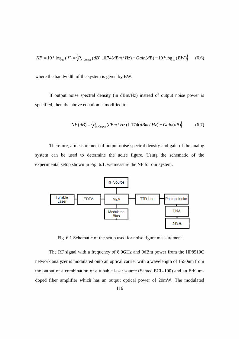
116
)(log*10)()/(174)()(log10 10,10 BWdBGainHzdBmdBPfNF OutputN −−+=∗= (6.6)
where the bandwidth of the system is given by BW.
If output noise spectral density (in dBm/Hz) instead of output noise power is
specified, then the above equation is modified to
)()/(174)/()( , dBGainHzdBmHzdBmPdBNF OutputN −+= (6.7)
Therefore, a measurement of output noise spectral density and gain of the analog
system can be used to determine the noise figure. Using the schematic of the
experimental setup shown in Fig. 6.1, we measure the NF for our system.
Fig. 6.1 Schematic of the setup used for noise figure measurement
The RF signal with a frequency of 8.0GHz and 0dBm power from the HP8510C
network analyzer is modulated onto an optical carrier with a wavelength of 1550nm from
the output of a combination of a tunable laser source (Santec ECL-100) and an Erbium-
doped fiber amplifier which has an output optical power of 20mW. The modulated
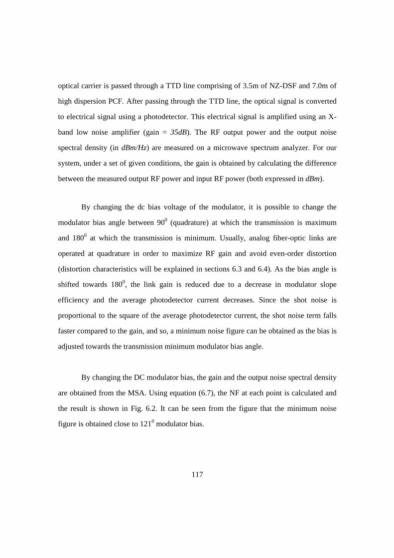
117
optical carrier is passed through a TTD line comprising of 3.5m of NZ-DSF and 7.0m of
high dispersion PCF. After passing through the TTD line, the optical signal is converted
to electrical signal using a photodetector. This electrical signal is amplified using an X-
band low noise amplifier (gain = 35dB). The RF output power and the output noise
spectral density (in dBm/Hz) are measured on a microwave spectrum analyzer. For our
system, under a set of given conditions, the gain is obtained by calculating the difference
between the measured output RF power and input RF power (both expressed in dBm).
By changing the dc bias voltage of the modulator, it is possible to change the
modulator bias angle between 900 (quadrature) at which the transmission is maximum
and 1800 at which the transmission is minimum. Usually, analog fiber-optic links are
operated at quadrature in order to maximize RF gain and avoid even-order distortion
(distortion characteristics will be explained in sections 6.3 and 6.4). As the bias angle is
shifted towards 1800, the link gain is reduced due to a decrease in modulator slope
efficiency and the average photodetector current decreases. Since the shot noise is
proportional to the square of the average photodetector current, the shot noise term falls
faster compared to the gain, and so, a minimum noise figure can be obtained as the bias is
adjusted towards the transmission minimum modulator bias angle.
By changing the DC modulator bias, the gain and the output noise spectral density
are obtained from the MSA. Using equation (6.7), the NF at each point is calculated and
the result is shown in Fig. 6.2. It can be seen from the figure that the minimum noise
figure is obtained close to 1210 modulator bias.
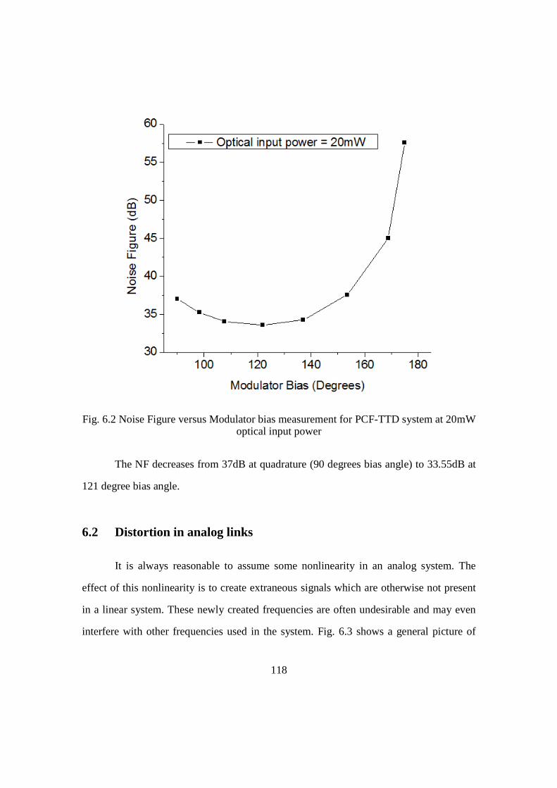
118
Fig. 6.2 Noise Figure versus Modulator bias measurement for PCF-TTD system at 20mW optical input power
The NF decreases from 37dB at quadrature (90 degrees bias angle) to 33.55dB at
121 degree bias angle.
6.2 Distortion in analog links
It is always reasonable to assume some nonlinearity in an analog system. The
effect of this nonlinearity is to create extraneous signals which are otherwise not present
in a linear system. These newly created frequencies are often undesirable and may even
interfere with other frequencies used in the system. Fig. 6.3 shows a general picture of
119
different distortion terms that affect an analog system within a given working bandwidth
(indicated by a yellow box).
Fig 6.3 Spectrum plot of output RF signals from a component having a nonlinear transfer function
6.2.1 HARMONIC DISTORTION
Any transfer function f(x) can be expanded in terms of a Taylor series as [2]
( )
hx
i
i
i
i
dx
fd
i
hxxf
∆=
∞
=
∆−+= ∑1 !
1)( (6.8)
For a linear device, all derivatives of the transfer function, except i=1 are zero.
Therefore, the output frequency follows the input frequency and no additional frequency
terms are generated. In the case of a non-linear transfer function, the derivatives are non
zero. Therefore, additional frequency components are generated in the output that differs

120
from the input frequency. If the additional components generated are such that they are
integral multiples fundamental frequency, then these components represent harmonic
(overtone) distortion. For example, if the fundamental frequency is f, then the harmonics
occur at 2f, 3f, 4f ….. mf etc, where m is an integer. The harmonic distortion components
are illustrated in Fig. 6.3 wherein two fundamental RF signals (represented with red
arrows) with frequencies f1 and f2 respectively produce second harmonic distortion
components 2f1 and 2f2 (represented with black dashed arrows). The higher order
harmonic distortion components are not shown for clarity. The useful bandwidth of the
analog system is also highlighted as a yellow box. If the bandwidth of the system is such
that the harmonic distortion terms appear outside the bandwidth, then these components
do not pose a problem for the system. If, however, the bandwidth of the system is large
enough to accommodate these harmonic terms, then addition band-pass filters need to be
used to eliminate these components. In practice, the bandwidth of systems is less than an
octave, and therefore, the harmonic powers lie outside the bandwidth of the system and
can be ignored.
6.2.2 INTERMODULATION DISTORTION
When two or more fundamental frequencies are present in the system, then apart
from components generated at integral multiples of fundamental frequencies, additional
components at the sum and difference of the any two fundamental frequencies also occur.
These sum and difference frequencies (second order) can in turn generate additional sum
and difference frequencies with other frequencies, providing components at sum and
difference of twice one frequency and the other frequency (third order) and so on. These
sum and difference frequency components are termed as intermodulation distortion
components. It can be seen from Fig. 6.3 that the second order intermodulation
121
components for fundamental frequencies f1 and f2 occur at (f1 + f2) and (f2 – f1)
(represented with blue arrows). These second order intermodulation terms usually lie
outside the useful bandwidth of the system and can be filtered out. The third order
intermodulation terms occur at (2f1 - f2) and (2f2 – f1) (represented with dashed green
arrows). However, these third order intermodulation terms occur inside the useful
bandwidth and can interfere with other useful signals at those frequencies. Therefore, it
becomes necessary to evaluate third order intermodulation distortion and determine how
these ‘spurious’ signals affect the working of the overall system.
6.3 Sources of distortion
Although noise in the system is present whether or not a signal source is present,
distortion on the other hand is present only when at least one signal source is present. In
our link, the optical signal from a CW laser source is modulated with the RF signal using
an electro-optic modulator. The modulated optical carrier is then transmitted using the
TTD lines and finally the optical signals are converted back to electrical signals at the
photodetector. For the levels of optical power carried by the delay lines, they can be
assumed to be linear devices. Therefore, the only sources of distortion in our link are the
modulator and the photodetector. Usually, in such analog optical links, distortion due to
modulator is more significant compared to that from the photodiode [1]. Therefore,
distortion measurement based on modulator will be described in this chapter.
122
6.4 Harmonic distortion measurement
The schematic diagram of the setup shown in Fig. 6.1 can be used to measure the
harmonic distortion in the highly dispersive photonic crystal fiber true time delay based
phased array antenna system.
An RF signal at a frequency of 8.0GHz with a power of 1mW is generated using
an HP 8510C network analyzer. Optical carrier from a tunable laser source with a
wavelength of 1550nm is amplified using an Erbium-doped fiber amplifier (EDFA). The
RF signal is modulated onto the amplified optical carrier using a Mach-Zehnder
modulator. This modulated signal is passed through a TTD line comprising of 3.5m of
NZ-DSF and 7.0m of highly dispersive PCF. After passing through the TTD line, the
optical signal is converted to electrical signal using a photodetector and amplified using a
low noise amplifier (LNA). The modulator bias is varied and the fundamental, second
harmonic and the third harmonic powers are measured on the microwave spectrum
analyzer and the measurement results are shown in Fig. 6.4.
It can be seen from the figure, that as the modulator bias is increased, the
fundamental, second and third harmonic signal powers become oscillatory. This is
because the transfer function of the modulator has a 2)(cosine relation. It can also be
seen that at the bias points wherein the fundamental power is maximum, the second
harmonic power is minimum. Therefore, by selecting the bias point as the maximum
transmission point (quadrature), second harmonic terms can be minimized. However, the
shape of the third order harmonic term follows that of the fundamental curve. It is
possible to select a bias point to eliminate the second order term, but not the third

123
harmonic term as even the fundamental signal is minimum at the point of minimum third
order power and is practically not useful.
In the PCF-TTD based phased array antenna system, the RF signals are in the X-
band (8-12.5GHz). Therefore, the second and third harmonic components at 16GHz and
24GHz respectively lie outside the useful bandwidth of the system and hence can be
neglected.
Fig. 6.4 Measured fundamental (black curve), second harmonic (red curve) and third harmonic (green) powers as a function of modulator bias
124
6.5 Intermodulation distortion measurement
It is clear from earlier discussion that the third order intermodulation distortion
products are important in any system as they appear within the useful bandwidth of the
system. For example, let us consider two closely spaced frequencies 9.0GHz and 9.1GHz
respectively which are in the X-band. The third order intermodulation products occur at
8.9GHz and 9.2GHz. Both these terms also appear within the useful bandwidth of the
system. If there are useful signals present at those frequencies, then these intermodulation
terms can interfere with the useful signal. These intermodulation terms are also termed
spurious as these are not the intended signals.
6.5.1 SPURIOUS-FREE DYNAMIC RANGE (SFDR)
A common way to measure distortion is to plot various output RF powers
(fundamental, second order, third-order etc) as a function of input signal power on a log-
log scale. The minimum power of the fundamental signal ( minP ) that the link can convey
information is when the fundamental power is equal to the noise power. The maximum
power of the fundamental signal (maxP ) that the link can convey information without
producing intermodulation products is when the distortion power is equal to the noise
power. Beyond this maximum input power, the distortion powers rise above the noise
floor and become appreciable. A measure of the intermodulation distortion is given by
the Spurious-Free Dynamic Range (SFDR) which is given by minmax PP − . Since the SFDR
is dependent on the noise power in the system, it is often convenient to provide the
dynamic range in a 1-Hz bandwidth.
125
On the log-log plot, the slope of the fundamental signal is unity and that of the
third-order IM is three. The slope of the lines gives the order of the output signal. A slope
of unity indicates fundamental signal and a slope of three indicates third order terms. This
means that the third-order intermodulation terms (IMD-3) rise or fall thrice as fast as the
fundamental signal. Therefore, as the input power is increased, the intermodulation
powers quickly rise above the noise floor. The point on the plot at which the fundamental
and third order intermodulation output powers intersect is called the third-order intercept
point (IIP3). The SFDR of an RF link limited by third-order intermodulation distortion
is given by [3, 4]
))174(3(3
2 −−∗= NFIIPSFDR (6.9)
where IIP3 is the linearly extrapolated input power (in dBm) where the fundamental and
third order curves intersect and NF is the link noise figure (in dB). The value of -174
refers to the noise power in dBm at a noise temperature of 290 K in a 1-Hz bandwidth.
6.5.2 SFDR MEASUREMENT
The experimental setup used to measure SFDR is shown in Fig. 6.5. An external
cavity laser source emits an optical carrier with wavelength 1550nm with an output
power of 5mW.
A high power Erbium-doped fiber amplifier (EDFA) from Amonics (which has a
maximum output power of 1Watt) is used to amplify the optical input power as required
and the amplified signal is passed through a polarization controller to the modulator. For
the current measurement, the gain of the EDFA is set to provide an optical output power
of 20mW. The closely spaced RF signals with frequencies 8GHz and 8.01GHz are
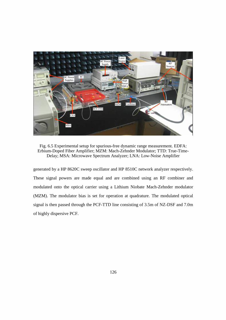
126
Fig. 6.5 Experimental setup for spurious-free dynamic range measurement. EDFA: Erbium-Doped Fiber Amplifier; MZM: Mach-Zehnder Modulator; TTD: True-Time-
Delay; MSA: Microwave Spectrum Analyzer; LNA: Low-Noise Amplifier
generated by a HP 8620C sweep oscillator and HP 8510C network analyzer respectively.
These signal powers are made equal and are combined using an RF combiner and
modulated onto the optical carrier using a Lithium Niobate Mach-Zehnder modulator
(MZM). The modulator bias is set for operation at quadrature. The modulated optical
signal is then passed through the PCF-TTD line consisting of 3.5m of NZ-DSF and 7.0m
of highly dispersive PCF.

127
Fig. 6.6 Fundamental and IMD-3 output powers as observed on a microwave spectrum analyzer
A high speed photodetector is used to convert the optical signal to electrical
signal. The electrical output signal is amplified using a low noise amplifier (LNA) and
the various output RF powers are measured on a microwave spectrum analyzer (MSA).
For the given fundamental frequencies, the third-order intermodulation products are
generated at 7.99GHz and 8.02 GHz. The fundamental and IMD-3 products are shown in
Fig. 6.6.
The fundamental input RF powers are changed and the corresponding
fundamental and IMD-3 output RF powers are measured and the results are plotted in
Fig. 6.7. The point of intersection of the fundamental RF output power line with the
vertical axis at the point where the fundamental input RF power is 0dBm gives the RF

128
gain of the system. Therefore, the RF gain of our system is 11dB. The third-order
intercept point (IIP3) is found to be 22dBm from the figure. The measured output noise
spectral density is also shown in the figure as a horizontal line.
Fig. 6.7 Fundamental (red squares) and IMD-3 (blue circles) RF output powers as a function of input RF power. Optical input power of 20mW and modulator bias angle of 90 degrees are used. Extrapolated straight line fits to the data points are also shown. The extrapolated lines intersect at a point whose corresponding RF input power gives IIP3
For the operating conditions of 20mW input optical power and 90 degrees
modulator bias, the noise figure of the system can be obtained from Fig. 6.2 as 37dB.
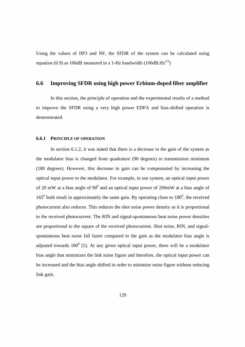
129
Using the values of IIP3 and NF, the SFDR of the system can be calculated using
equation (6.9) as 106dB measured in a 1-Hz bandwidth (106dB.Hz2/3)
6.6 Improving SFDR using high power Erbium-doped fiber amplifier
In this section, the principle of operation and the experimental results of a method
to improve the SFDR using a very high power EDFA and bias-shifted operation is
demonstrated.
6.6.1 PRINCIPLE OF OPERATION
In section 6.1.2, it was stated that there is a decrease in the gain of the system as
the modulator bias is changed from quadrature (90 degrees) to transmission minimum
(180 degrees). However, this decrease in gain can be compensated by increasing the
optical input power to the modulator. For example, in our system, an optical input power
of 20 mW at a bias angle of 900 and an optical input power of 200mW at a bias angle of
1650 both result in approximately the same gain. By operating close to 1800, the received
photocurrent also reduces. This reduces the shot noise power density as it is proportional
to the received photocurrent. The RIN and signal-spontaneous beat noise power densities
are proportional to the square of the received photocurrent. Shot noise, RIN, and signal-
spontaneous beat noise fall faster compared to the gain as the modulator bias angle is
adjusted towards 1800 [5]. At any given optical input power, there will be a modulator
bias angle that minimizes the link noise figure and therefore, the optical input power can
be increased and the bias angle shifted in order to minimize noise figure without reducing
link gain.
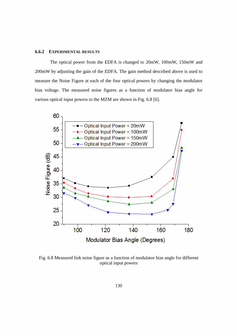
130
6.6.2 EXPERIMENTAL RESULTS
The optical power from the EDFA is changed to 20mW, 100mW, 150mW and
200mW by adjusting the gain of the EDFA. The gain method described above is used to
measure the Noise Figure at each of the four optical powers by changing the modulator
bias voltage. The measured noise figures as a function of modulator bias angle for
various optical input powers to the MZM are shown in Fig. 6.8 [6].
Fig. 6.8 Measured link noise figure as a function of modulator bias angle for different optical input powers
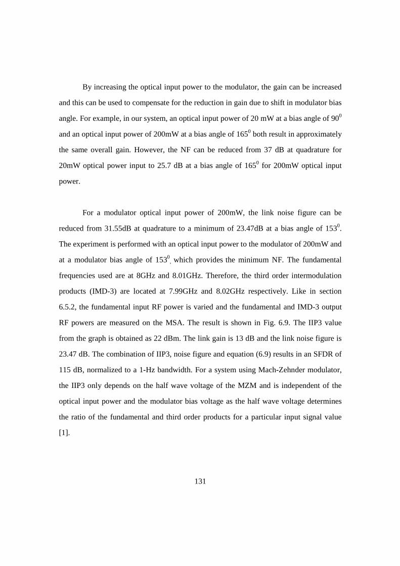
131
By increasing the optical input power to the modulator, the gain can be increased
and this can be used to compensate for the reduction in gain due to shift in modulator bias
angle. For example, in our system, an optical input power of 20 mW at a bias angle of 900
and an optical input power of 200mW at a bias angle of 1650 both result in approximately
the same overall gain. However, the NF can be reduced from 37 dB at quadrature for
20mW optical power input to 25.7 dB at a bias angle of 1650 for 200mW optical input
power.
For a modulator optical input power of 200mW, the link noise figure can be
reduced from 31.55dB at quadrature to a minimum of 23.47dB at a bias angle of 1530.
The experiment is performed with an optical input power to the modulator of 200mW and
at a modulator bias angle of 1530, which provides the minimum NF. The fundamental
frequencies used are at 8GHz and 8.01GHz. Therefore, the third order intermodulation
products (IMD-3) are located at 7.99GHz and 8.02GHz respectively. Like in section
6.5.2, the fundamental input RF power is varied and the fundamental and IMD-3 output
RF powers are measured on the MSA. The result is shown in Fig. 6.9. The IIP3 value
from the graph is obtained as 22 dBm. The link gain is 13 dB and the link noise figure is
23.47 dB. The combination of IIP3, noise figure and equation (6.9) results in an SFDR of
115 dB, normalized to a 1-Hz bandwidth. For a system using Mach-Zehnder modulator,
the IIP3 only depends on the half wave voltage of the MZM and is independent of the
optical input power and the modulator bias voltage as the half wave voltage determines
the ratio of the fundamental and third order products for a particular input signal value
[1].

132
It can be seen that the improvement in the SFDR of the system from 106dB.Hz2/3
to 115dB.Hz2/3 can be achieved by simply controlling the dc modulator bias and using a
very high power EDFA without using any other optical or electronic linearization
schemes. Although the EDFA can provide up to 1W of optical power, the fundamental
limitation in achieving very high SFDR is the optical power handling capacity of the
modulator, which is 200mW for our device. Utilizing higher power handling MZMs, the
SFDR can further be improved.
Fig. 6.9 Fundamental (red squares) and IMD-3 (blue circles) RF output powers as a function of input RF power. Optical input power of 200mW and modulator bias angle of 153 degrees are used. Extrapolated straight line fits to the data points are also shown. The extrapolated lines intersect at a point whose corresponding RF input power gives IIP3

133
6.7 Summary
In this chapter, RF performance characterization of the PCF TTD-based phased
array antenna system was performed. Experiments were performed to evaluate the noise
performance and distortion characteristics of the system by measuring the noise figure
and harmonic distortion. An important parameter related to the performance of the
system, namely the Spurious-Free Dynamic Range (SFDR) was presented and measured
to be 106dB for the system with 20mW optical input power to the modulator at
quadrature in a 1-Hz bandwidth. The SFDR of the system was improved using a high
power EDFA and bias shifted operation. SFDR as high as 115dB in a 1-Hz bandwidth
was achieved for an optical power input of 200mW and bias shifted to 153 degrees.
6.8 References
[1] C. H. Cox, Analog Optical Links: Theory and Practice. Cambridge, U.K. Cambridge Univ. Press (2004)
[2] P. Dienes, The Taylor Series, An Introduction to the Theory of Functions of a Complex Variable, Clarendon Press, Oxford (1931), reprint: Dover, New York (1957)
[3] A. Karim and J. Devenport, “High Dynamic Range Microwave Photonic Links for RF Signal Transport and RF-IF Conversion,” J. Lightwave. Technol. 26, pp. 2718-2724 (2008)
[4] A. Karim and J. Davenport, “Noise Figure Reduction in Externally Modulated Analog Fiber-Optic Links,” IEEE. Photon. Technol. Letts. 19, pp. 312-314 (2007)
[5] G. E. Betts, J. P. Donnelly, J. N.Walpole, S. H. Groves, F. J. O’Donnell, L. J. Missaggia, R. J. Bailey, and A. Napoleone, “Semiconductor laser sources for externally modulated microwave analog links,” IEEE Trans. Microw. Theory Tech. vol. 45, pp. 1280–1287 (1997)
[6] H. Subbaraman, M. Y. Chen, and R. T. Chen, “Spurious-Free Dynamic Range (SFDR) improvement in a true-time-delay system based on highly dispersive

134
photonic crystal fiber,” in IEEE/LEOS Winter Topical Meeting Series, pp. 58-59, Innsbruck, Austria (2009)

135
Chapter 7 X-band Sparse Array Antenna Demonstration
In this Chapter, the need to use a sparse array antenna for modern applications
will be briefly discussed. Characteristic features of such antennas along with simulation
results will be provided. Using the PCF-TTD module, experiment will be setup and
preliminary beam steering results will be demonstrated for an X-band sparse array using
3 horn antennas which is equivalent to a 29 element standard array. Due to the limitation
of the lengths of PCF in the TTD module, wider steering angles cannot be demonstrated.
Therefore, another dispersive fiber module will be constructed using dispersion
compensation fibers and the sparse array beam steering will be demonstrated.
7.1 Why do we require a sparse array?
A standard antenna array consists of antenna elements which are spaced half a
wavelength apart according to the relation given in equation (1.11) in order to avoid
grating lobes. In order to achieve a very narrow beam, a very large array needs to be used
as the beam width is inversely proportional to the size of the array [1]. However, the
weight and size of the antenna elements becomes extremely critical for applications such
as phased array radar and satellite communications. Therefore, it becomes very important
to be able to synthesize the required radiation pattern by using a minimum number of
antenna elements. Also, the use of such a sparse array will eliminate complex
computational capability that would otherwise be required in a standard array consisting
of a large number of elements. The reduction in the number of elements also reduces the
cost and the eases the construction of the array. It is possible to create an antenna array

136
with fewer elements to produce narrow beam widths. Such antenna arrays are called
sparse antenna arrays.
7.1.1 SIMULATION RESULTS
The simulated array factor of a 100 element standard antenna array is shown in
Fig. 7.1. The inter-element spacing is equal to half wavelength at 12.5GHz. The
normalized pattern for a beam radiated broadside is shown. It can be seen from the figure
that the large array provides a characteristic narrow ‘pencil’ like beam. However, such an
array is not only cost prohibitive, but is also heavy and congested. Complex computation
for large number of signals received from all the elements is also required.
Fig. 7.1 Array factor simulation of a 100 element standard array with inter-element
spacing 2λ=d at 12.5GHz
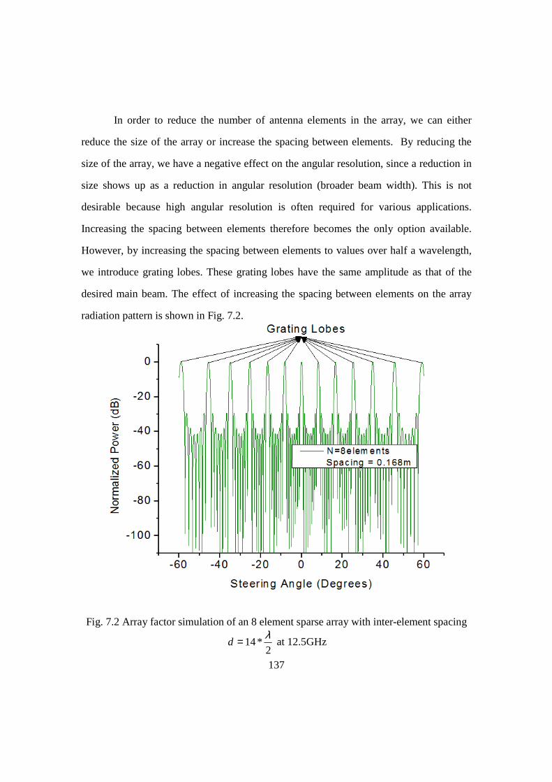
137
In order to reduce the number of antenna elements in the array, we can either
reduce the size of the array or increase the spacing between elements. By reducing the
size of the array, we have a negative effect on the angular resolution, since a reduction in
size shows up as a reduction in angular resolution (broader beam width). This is not
desirable because high angular resolution is often required for various applications.
Increasing the spacing between elements therefore becomes the only option available.
However, by increasing the spacing between elements to values over half a wavelength,
we introduce grating lobes. These grating lobes have the same amplitude as that of the
desired main beam. The effect of increasing the spacing between elements on the array
radiation pattern is shown in Fig. 7.2.
Fig. 7.2 Array factor simulation of an 8 element sparse array with inter-element spacing
2*14
λ=d at 12.5GHz

138
The figure shows the normalized array factor of a sparse array consisting of 8
elements with inter-element distance equal to2
*14λ
. The overall dimension of the array
is approximately equal to that of a standard 100 element array. It can be seen from the
figure that although the beam width of the central beam at 0 degree steering angle is
small, there are several lobes which have almost the same characteristics as that of the
desired beam. These grating lobes or aliases occur at equal angle separations and are
undesirable and hence need to be minimized or eliminated.
The overall far-field radiation pattern is obtained by multiplying the array factor
with the antenna element pattern. If however, we choose an antenna element radiation
pattern that has nulls at the places where there are grating lobes in the array factor, then
the grating lobes can be totally eliminated. However, such an array antenna can only
radiate broadside without grating lobes and the antenna head has to be rotated
mechanically in order to steer the beam. This is because, if the beam is steered
electronically, then the nulls do not exactly line up with the grating lobes, and the effect
of grating lobes starts getting predominant. Mechanically moving the antenna array head
defeats the purpose of a phased array antenna which has the advantage of beam steering
without mechanical movement of the antenna array.
It is possible to form a sparse array wherein the antenna elements are
aperiodically spaced [2-3]. Due to non-uniform antenna element spacing, the grating
lobes no longer appear at equal angle separations. The grating lobes become wider and
less sensitive. Many groups [4-7] have demonstrated sparse arrays designed with
aperiodic spacing with reduced grating lobe levels.

139
In this chapter, preliminary work on the use of highly dispersive photonic crystal
fibers and another highly dispersive fiber TTD module for a 3 element periodically
spaced X-band sparse array are presented. The three elements are spaced to imitate a 29
element standard array. A three element sparse array is chosen because of the limitation
of availability of minimum far-field distance in the laboratory.
7.2 Sparse Array Antenna
The X-band sparse antenna array constructed using 3 horn antenna elements is
shown in Fig. 7.3. The base plate is fixed on a precision rotation stage.
Fig. 7.3 X-band sparse array antenna consisting of three periodically spaced horn antennas spaced 0.168m apart, equivalent to a 29-element standard array (precision
rotation stage is also shown)
The antenna element has a gain of 6dB. The three horn antennas are spaced
0.168m apart, and this is equivalent to a 29 element standard array. In order to ascertain
the frequency of maximum transmission, the reflection coefficient (S11) of 3 antenna

140
elements as a function of frequencies is measured using the network analyzer. The
measured result is shown in Fig. 7.4. It can be seen from the figure that minimum
reflections (minimum S11) occur near 9GHz and 10GHz. Therefore, all experiments are
performed at these two frequencies.
Fig. 7.4 Measured S11 parameter of three antenna elements
In order to simulate the far-field radiation pattern, the element pattern needs to be
incorporated into the simulation. By multiplying the simulated array factor with a
measured element pattern, the far-field radiation pattern of the sparse array can be
simulated. In order to measure the element pattern of the antenna element, the antenna is

141
placed on a precision rotation stage and the radiated power is measured using the MSA at
a distance greater than the antenna’s far-field as a function of angle. The element patterns
of the antenna element are measured at 9GHz and 10GHz and are shown in figures 7.5(a)
and 7.5(b) respectively.
Fig. 7.5 Measured normalized patterns of 3 antenna elements at a frequency of (a) 9GHz and (b) 10GHz
Compared to the element pattern of the patch antenna that was shown in Fig. 4.3,
the radiation pattern of the horn antenna has a strong dependence on the steering angle.
Therefore, the beams at larger angles experience suppression compared to beams closer
to broadside. This element pattern acts as a filter at larger angles and so, the desired beam
at larger angles will have a lower power.
7.3 Highly dispersive PCF TTD based sparse array system
Since one of the primary objectives of a sparse array system is to reduce the size
and weight of the system, the sparse array system can greatly benefit from highly
dispersive photonic crystal fibers. In order to demonstrate the working of the sparse
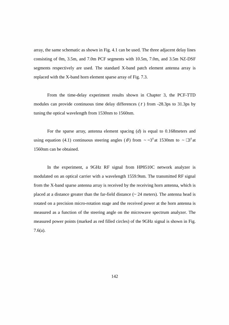
142
array, the same schematic as shown in Fig. 4.1 can be used. The three adjacent delay lines
consisting of 0m, 3.5m, and 7.0m PCF segments with 10.5m, 7.0m, and 3.5m NZ-DSF
segments respectively are used. The standard X-band patch element antenna array is
replaced with the X-band horn element sparse array of Fig. 7.3.
From the time-delay experiment results shown in Chapter 3, the PCF-TTD
modules can provide continuous time delay differences (τ ) from -28.3ps to 31.3ps by
tuning the optical wavelength from 1530nm to 1560nm.
For the sparse array, antenna element spacing (d) is equal to 0.168meters and
using equation (4.1) continuous steering angles (θ ) from 03~ − at 1530nm to 03~ + at
1560nm can be obtained.
In the experiment, a 9GHz RF signal from HP8510C network analyzer is
modulated on an optical carrier with a wavelength 1559.9nm. The transmitted RF signal
from the X-band sparse antenna array is received by the receiving horn antenna, which is
placed at a distance greater than the far-field distance (~ 24 meters). The antenna head is
rotated on a precision micro-rotation stage and the received power at the horn antenna is
measured as a function of the steering angle on the microwave spectrum analyzer. The
measured power points (marked as red filled circles) of the 9GHz signal is shown in Fig.
7.6(a).
143
Fig. 7.6 Simulated and Measured far-field radiation patterns of the sparse array antenna at an optical wavelength of (a) 1559.9nm corresponding to +3degree beam steering and (b)
1529.9nm corresponding to -3degree beam steering (blue arrows indicate the desired beam, dashed red arrows at 0degree indicate the beam steering angle at center wavelength
of 1545nm)
144
Similarly, the experiment is also performed for a 10GHz signal. The measured far
field radiation pattern points (marked as green squares) of a 10GHz signal modulated on
an optical carrier with wavelength 1559.9nm is shown in the same figure. The simulated
far field radiation patterns are shown in figure as dashed curves. The far-field radiation
patterns at the two frequencies are also measured by tuning the optical wavelength to
1529.9nm and the result is shown in Fig. 7.6(b). In both the figures, the desired beam is
marked with a blue arrow. At the central wavelength of 1545nm, the desired beam would
be directed at 0 degrees (indicated by dashed red arrows).
It can be seen from the figures that the maximum transmitted power occurs at +3
degrees at a wavelength of 1559.9nm and -3 degrees at a wavelength of 1529.9nm
respectively, for 9GHz and 10GHz signals, thus showing a beam squint free operation.
The different grating lobes that occur due to the spacing of the antenna elements are also
evident. These lobes are lower in amplitude compared to the main lobe due to the
filtering action of the horn element pattern. However, due to the limitation in the
maximum achievable time delay due to the available length of PCF in the TTD modules,
angles beyond 3 degrees from the sparse array system cannot been demonstrated using
PCF-TTD module.
7.4 Highly dispersive fiber-based sparse array antenna system
In order to demonstrate angles greater than 3± degrees, we constructed another
true-time-delay module with 4 delay lines, each consisting of a length of dispersion
compensation fiber (Corning® Vast Dispersion Compensating Fiber) connected to a
length of NZ-DSF (Corning® LEAF fiber). The total length of fibers (DCF and NZ-DSF)
145
in each delay line is equal to 720meters. The lengths of DCF in the 4 lines are 0m, 230m,
460m, and 690m. The dispersion coefficient of the DCF is equal to kmnmps //5.120− at
1545nm.
7.4.1 TIME DELAY MEASUREMENT
In order to obtain the chromatic dispersion of the DCF, the time delay difference
( T∆ ) between optical wavelengths of 1.0±λ nm was measured at each wavelength
according to the setup explained in [8]. The delay line consisting of 690m of DCF and
30m of NZ-DSF was used for this purpose. In order to measure the time delay difference,
the phase difference as a function of microwave frequency is measured at optical
wavelengths of ( 1.0+λ nm) and ( 1.0−λ nm). The slope of the phase versus frequency
curve gives the time delay. The dispersion coefficient is calculated using
)/( LTD ⋅∆∆= λ (7.1)
where λ∆ is the wavelength difference = 0.2 nm and L is the length of DCF = 690m
(contribution to time delay difference from non-zero dispersion shifted fiber is
negligible). The measured group velocity dispersion curve as a function of wavelength is
shown in table 7.1.
Using the dispersion coefficient values and equations (1.14) and (1.20), the
steering angles can be calculated at a central wavelength chosen as 1555nm. A TTD
module consisting of 3 delay lines if formed by connecting different lengths of DSF with
different lengths of NZ-DSF in each line.
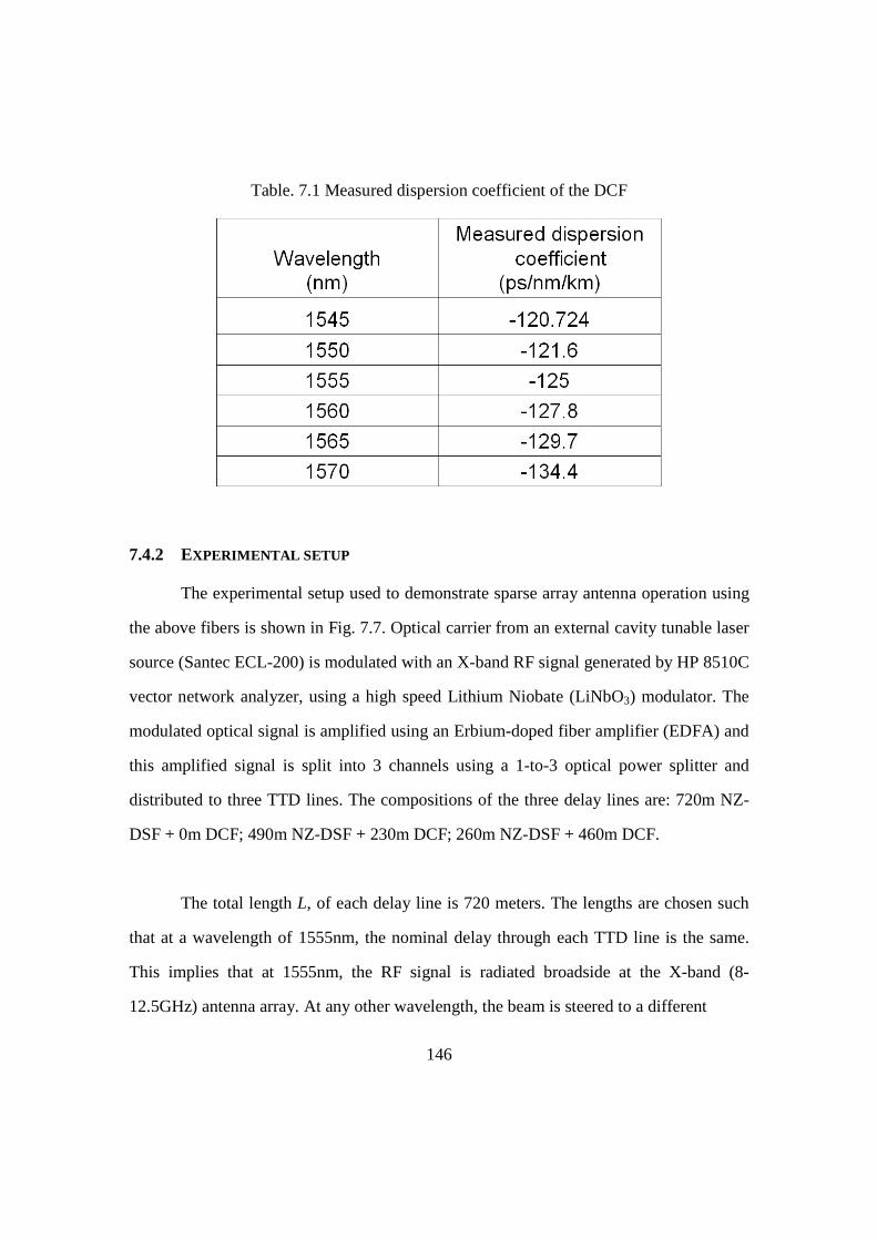
146
Table. 7.1 Measured dispersion coefficient of the DCF
7.4.2 EXPERIMENTAL SETUP
The experimental setup used to demonstrate sparse array antenna operation using
the above fibers is shown in Fig. 7.7. Optical carrier from an external cavity tunable laser
source (Santec ECL-200) is modulated with an X-band RF signal generated by HP 8510C
vector network analyzer, using a high speed Lithium Niobate (LiNbO3) modulator. The
modulated optical signal is amplified using an Erbium-doped fiber amplifier (EDFA) and
this amplified signal is split into 3 channels using a 1-to-3 optical power splitter and
distributed to three TTD lines. The compositions of the three delay lines are: 720m NZ-
DSF + 0m DCF; 490m NZ-DSF + 230m DCF; 260m NZ-DSF + 460m DCF.
The total length L, of each delay line is 720 meters. The lengths are chosen such
that at a wavelength of 1555nm, the nominal delay through each TTD line is the same.
This implies that at 1555nm, the RF signal is radiated broadside at the X-band (8-
12.5GHz) antenna array. At any other wavelength, the beam is steered to a different

147
Fig. 7.7 Experimental setup for sparse array antenna demonstration, LNA: low-noise amplifier; MZM: Mach-Zehnder modulator; TTD: true-time-delay
direction depending on the time delay differences between adjacent delay lines. A
photodetector bank converts the optical signals into electrical signals. Electrical tunable
delay lines are used to fine tune the delays such that the delay through all TTD lines are
equal at a wavelength of 1555nm. These signals are then amplified by an X-band low
noise amplifier (LNA). After amplification, the electrical signals are fed to the 3 horn
antenna elements of an antenna array, which has an element spacing of 0.168m. The far
field radiation pattern of the X-band PAA is measured by fixing the antenna array on an
accurate positioner and measuring the received power by a fixed standard horn antenna
connected to a microwave spectrum analyzer (MSA) at a distance greater than the far-
field distance.
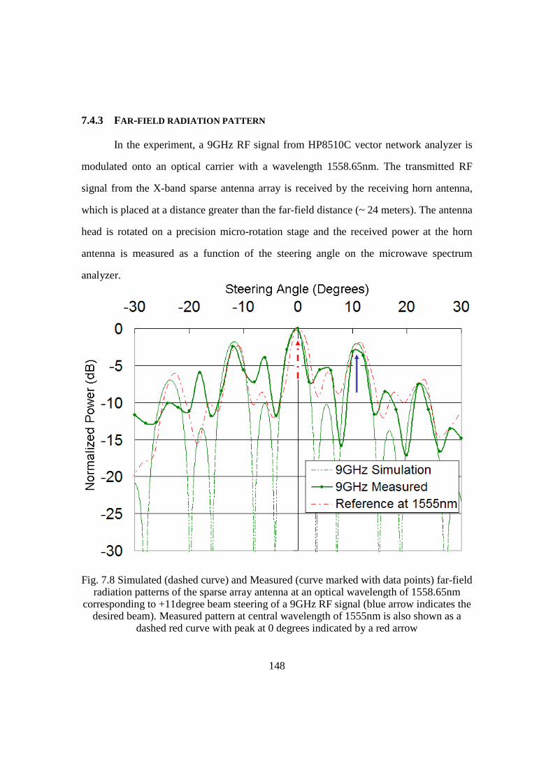
148
7.4.3 FAR-FIELD RADIATION PATTERN
In the experiment, a 9GHz RF signal from HP8510C vector network analyzer is
modulated onto an optical carrier with a wavelength 1558.65nm. The transmitted RF
signal from the X-band sparse antenna array is received by the receiving horn antenna,
which is placed at a distance greater than the far-field distance (~ 24 meters). The antenna
head is rotated on a precision micro-rotation stage and the received power at the horn
antenna is measured as a function of the steering angle on the microwave spectrum
analyzer.
Fig. 7.8 Simulated (dashed curve) and Measured (curve marked with data points) far-field radiation patterns of the sparse array antenna at an optical wavelength of 1558.65nm
corresponding to +11degree beam steering of a 9GHz RF signal (blue arrow indicates the desired beam). Measured pattern at central wavelength of 1555nm is also shown as a
dashed red curve with peak at 0 degrees indicated by a red arrow

149
The far field radiation pattern of a 9GHz signal at the central wavelength of
1555nm is measured and the result is shown in Fig. 7.8 by a dashed red curve. It can be
seen that the central wavelength, the beam is steered to 00 as indicated by a dashed red
arrow. Next, the far field radiation pattern is measured by tuning the wavelength to
1558.65nm. It can be seen that the beam is steered to +110 (marked by a blue arrow). The
simulated and measured patterns are shown by dashed and solid green patterns,
respectively. Unequal levels of the intended main lobe (indicated by a blue arrow) and
the grating lobes are due to the filtering action of the horn antenna radiation pattern. The
individual horn element pattern is measured separately and included in the simulation. It
can be seen from the figure that the measured and simulated curves agree well with each
other. Beam squint-free operation is also demonstrated by steering 9GHz and 10GHz
signals to -150 (with respect to 00 at 1555nm) by tuning the wavelength to 1550nm as
shown in Fig. 7.9. The intended beam (indicated by blue arrow) has peak at -150.
By employing highly dispersive photonic crystal fibers along with a properly
designed aperiodic sparse array antenna, the size and weight of the system along with the
levels of grating lobes can be reduced, thus providing a very useful system for air-borne
and satellite applications. In this work, we designed a simple sparse array with periodic
spacing between elements to show the working of the sparse array system.

150
Fig. 7.9 Simulated (dashed smooth curves) and Measured (curves marked with data points) far-field radiation patterns of the sparse array antenna at an optical wavelength of 1550nm corresponding to -15degree beam steering of a 9GHz (red curves) and a 10GHz
RF signal (green curves)
7.5 Summary
In this chapter, the need for a sparse array antenna was briefly discussed. An X-
band sparse array antenna was constructed using 3 horn antenna elements with spacing
such that the array was equivalent to a 29 element standard array. The working of the
sparse array was shown by utilizing PCF-TTD module and demonstrating beam steering
of two frequencies, 9GHz and 10GHz, to +3 degrees and -3 degrees by tuning the
wavelength to 1559.9nm and 1529.9nm respectively. Another TTD module was created
using dispersion compensation fibers and NZ-DSF fibers and beam steering results

151
beyond 3± degrees were demonstrated. 9GHz and 10GHz RF signals were steered to -15
degrees and +11 degrees by tuning the wavelength to 1550nm and 1558.65nm
respectively. Such a sparse antenna array has the potential to reduce the size and weight
of future systems.
7.6 References
[1] H. J. Visser, Array and Phased Array Antenna Basics, John Wiley and Sons Ltd (2005)
[2] Y. Liu, Z. Nie, and Q. Liu, “Reducing the number of elements in a linear antenna array by the matrix pencil method,” IEEE. Trans. Antennas. Propag. vol. 56, pp. 2955-2962 (2008)
[3] B. P. Kumar and G. R. Branner, “Design of Unequally Spaced Arrays for Performance Improvement,” IEEE. Trans. Antennas. Propag. vol. 47, pp. 511-523 (1999)
[4] R. L. Haupt, “Thinned arrays using genetic algorithms,” IEEE Trans. Antennas. Propag. vol. 42, pp. 993–999 (1994)
[5] M. G. Bray, D. H. Werner, D. W. Boeringer, and D. W. Machuga, “Optimization of thinned aperiodic linear phased arrays using genetic algorithms to reduce grating lobes during scanning,” IEEE. Trans. Antennas. Propag. vol. 50, pp. 1732–1742 (2002)
[6] T. G. Spence and D. H. Werner, “Design of Broadband Planar Arrays Based on the Optimization of Aperiodic Tilings,” IEEE. Trans. Antennas. Propag. vol. 56, pp. 76-86 (2008)
[7] D. S. Goshi, K. M. K. H. Leong, and T. Itoh, “A Sparsely Designed Retrodirective Transponder,” IEEE. Antennas. Wireless. Propag. Letts. vol. 5, pp. 339-342 (2006)
[8] B. Howley, Z. Shi, Y. Jiang, and R. T. Chen, “Thermally tuned optical fiber for true time delay generation,” Opt. Laser Technol. vol. 37, pp. 29-32, (2004)
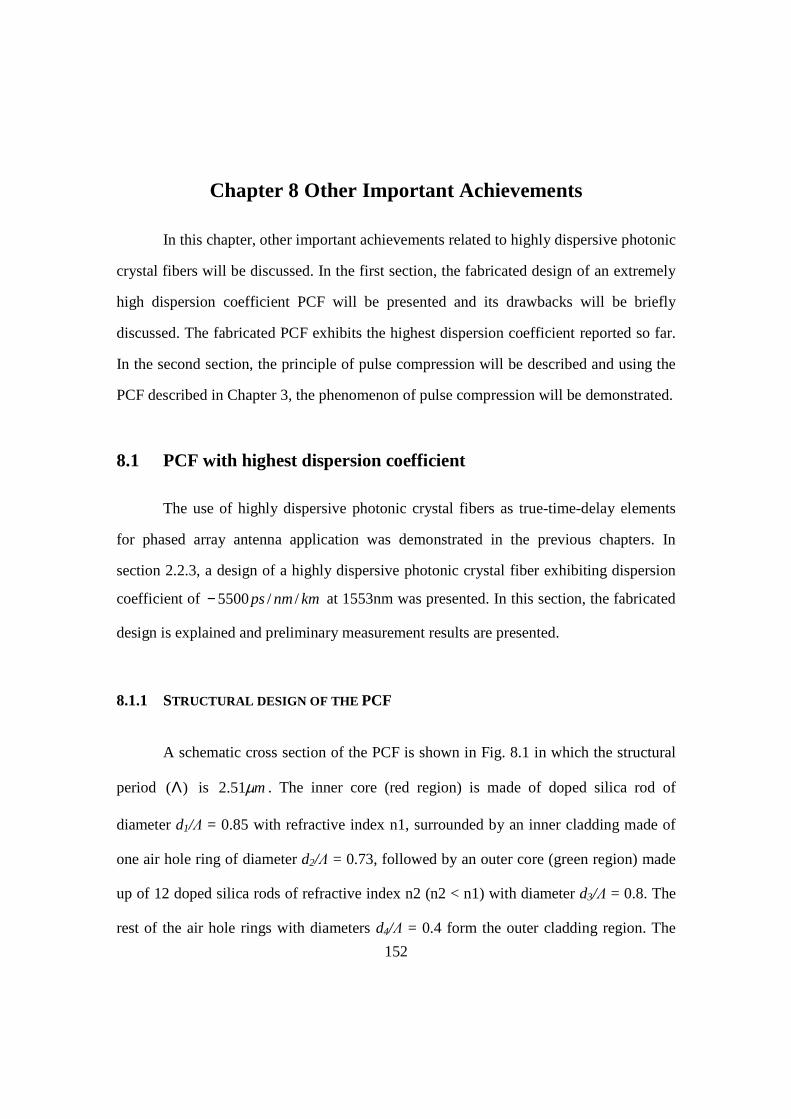
152
Chapter 8 Other Important Achievements
In this chapter, other important achievements related to highly dispersive photonic
crystal fibers will be discussed. In the first section, the fabricated design of an extremely
high dispersion coefficient PCF will be presented and its drawbacks will be briefly
discussed. The fabricated PCF exhibits the highest dispersion coefficient reported so far.
In the second section, the principle of pulse compression will be described and using the
PCF described in Chapter 3, the phenomenon of pulse compression will be demonstrated.
8.1 PCF with highest dispersion coefficient
The use of highly dispersive photonic crystal fibers as true-time-delay elements
for phased array antenna application was demonstrated in the previous chapters. In
section 2.2.3, a design of a highly dispersive photonic crystal fiber exhibiting dispersion
coefficient of kmnmps //5500− at 1553nm was presented. In this section, the fabricated
design is explained and preliminary measurement results are presented.
8.1.1 STRUCTURAL DESIGN OF THE PCF
A schematic cross section of the PCF is shown in Fig. 8.1 in which the structural
period )(Λ is mµ51.2 . The inner core (red region) is made of doped silica rod of
diameter d1/Λ = 0.85 with refractive index n1, surrounded by an inner cladding made of
one air hole ring of diameter d2/Λ = 0.73, followed by an outer core (green region) made
up of 12 doped silica rods of refractive index n2 (n2 < n1) with diameter d3/Λ = 0.8. The
rest of the air hole rings with diameters d4/Λ = 0.4 form the outer cladding region. The

153
central core with refractive index n1 is positively doped and has a doping concentration
that raises its refractive index by 1.35% compared to background silica (yellow region).
The outer core with refractive index n2 is negatively doped and has a doping
concentration that lowers its refractive index by -0.7% compared to background silica [1].
The values of the parameters are chosen in such a way that the phase matched
wavelength is around 1.55 µm.
Λ
d1d2 d3d4
Λ
d1d2 d3d4
Fig. 8.1 Cross section of the designed photonic crystal fiber. The periodicity of the structure is given by Λ. A high index central core (d1) is surrounded by an inner cladding (d2) consisting of air holes. Outer core (d3) has slightly lower refractive index compared
to the central core. All other air holes (d4) form the outer cladding region
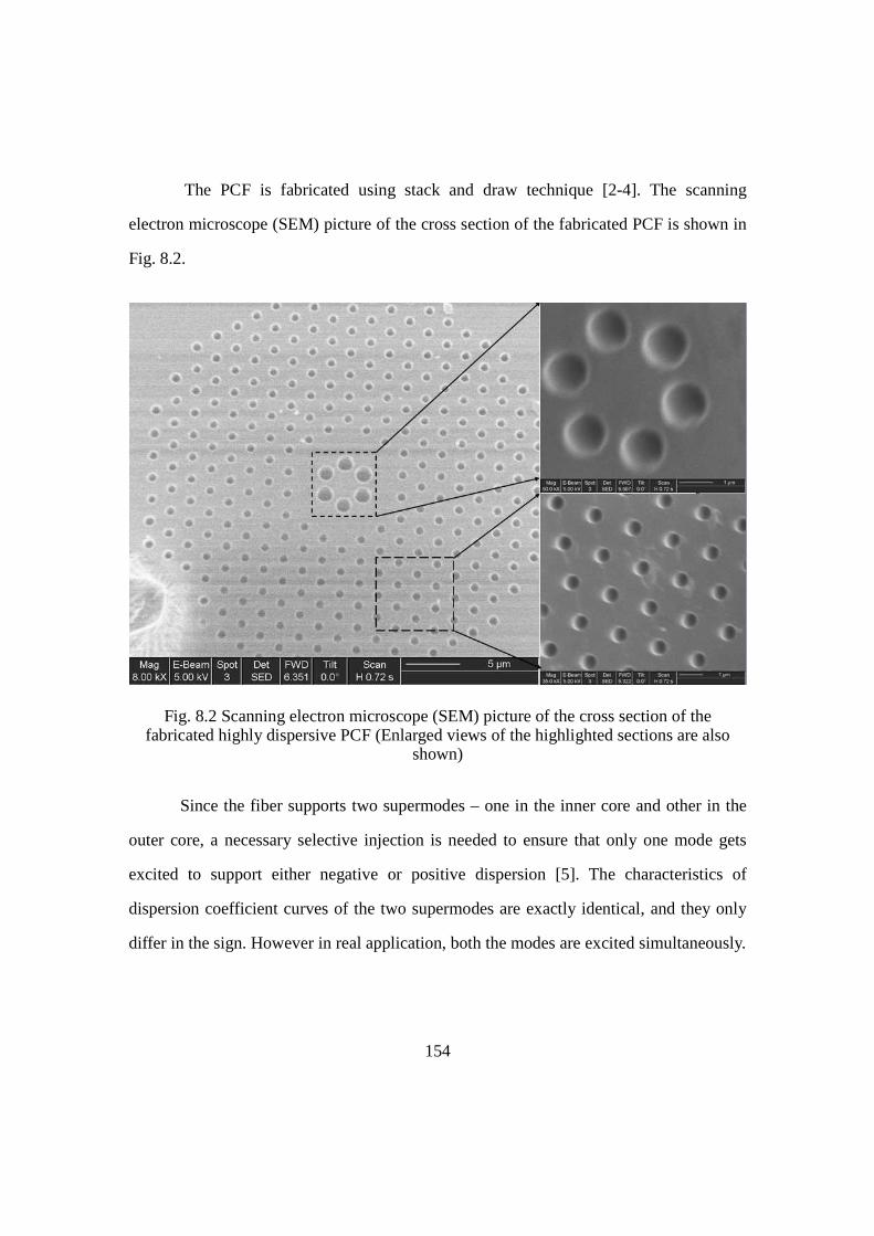
154
The PCF is fabricated using stack and draw technique [2-4]. The scanning
electron microscope (SEM) picture of the cross section of the fabricated PCF is shown in
Fig. 8.2.
Fig. 8.2 Scanning electron microscope (SEM) picture of the cross section of the fabricated highly dispersive PCF (Enlarged views of the highlighted sections are also
shown)
Since the fiber supports two supermodes – one in the inner core and other in the
outer core, a necessary selective injection is needed to ensure that only one mode gets
excited to support either negative or positive dispersion [5]. The characteristics of
dispersion coefficient curves of the two supermodes are exactly identical, and they only
differ in the sign. However in real application, both the modes are excited simultaneously.
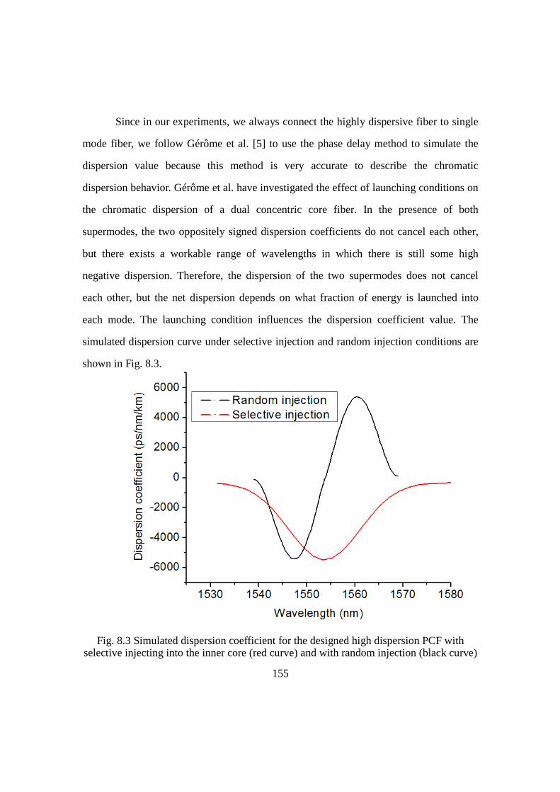
155
Since in our experiments, we always connect the highly dispersive fiber to single
mode fiber, we follow Gérôme et al. [5] to use the phase delay method to simulate the
dispersion value because this method is very accurate to describe the chromatic
dispersion behavior. Gérôme et al. have investigated the effect of launching conditions on
the chromatic dispersion of a dual concentric core fiber. In the presence of both
supermodes, the two oppositely signed dispersion coefficients do not cancel each other,
but there exists a workable range of wavelengths in which there is still some high
negative dispersion. Therefore, the dispersion of the two supermodes does not cancel
each other, but the net dispersion depends on what fraction of energy is launched into
each mode. The launching condition influences the dispersion coefficient value. The
simulated dispersion curve under selective injection and random injection conditions are
shown in Fig. 8.3.
Fig. 8.3 Simulated dispersion coefficient for the designed high dispersion PCF with selective injecting into the inner core (red curve) and with random injection (black curve)
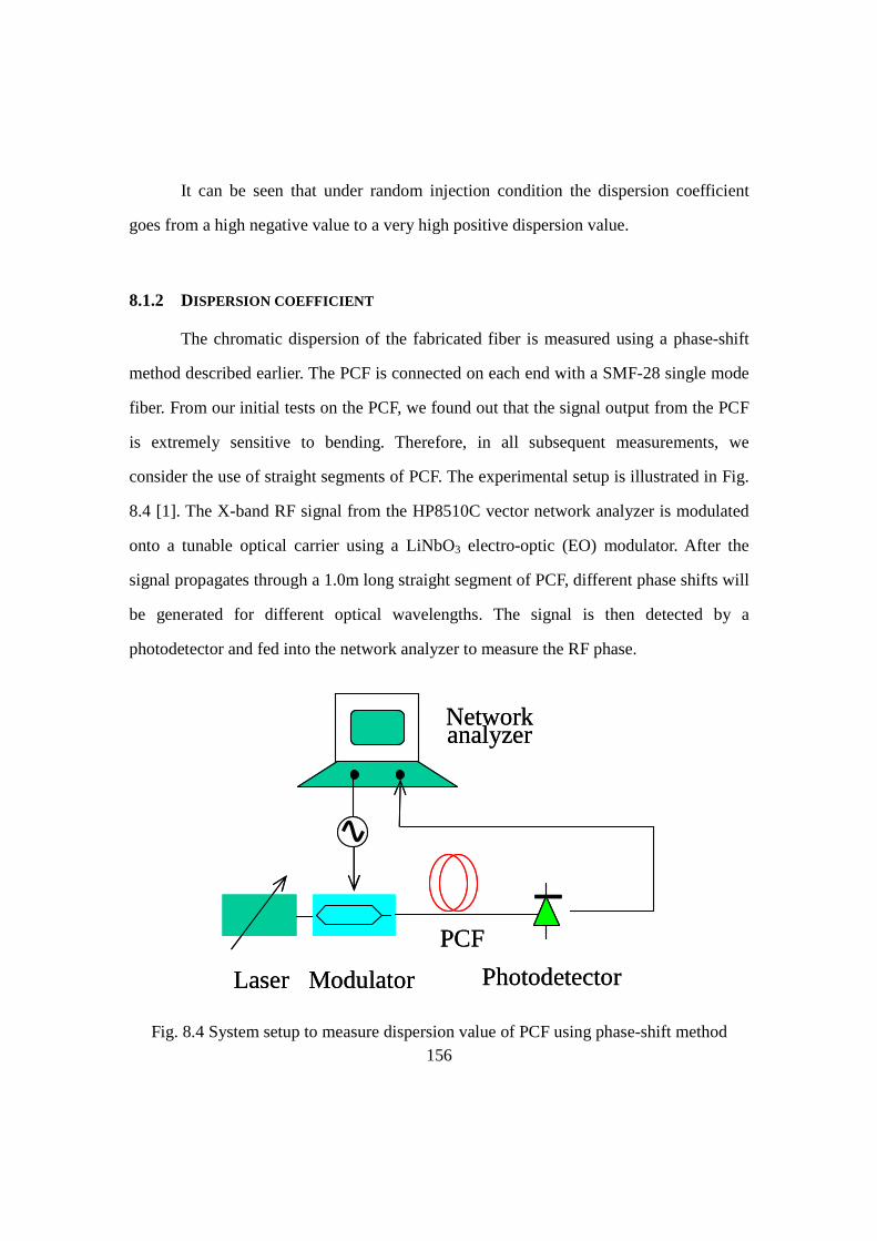
156
It can be seen that under random injection condition the dispersion coefficient
goes from a high negative value to a very high positive dispersion value.
8.1.2 DISPERSION COEFFICIENT
The chromatic dispersion of the fabricated fiber is measured using a phase-shift
method described earlier. The PCF is connected on each end with a SMF-28 single mode
fiber. From our initial tests on the PCF, we found out that the signal output from the PCF
is extremely sensitive to bending. Therefore, in all subsequent measurements, we
consider the use of straight segments of PCF. The experimental setup is illustrated in Fig.
8.4 [1]. The X-band RF signal from the HP8510C vector network analyzer is modulated
onto a tunable optical carrier using a LiNbO3 electro-optic (EO) modulator. After the
signal propagates through a 1.0m long straight segment of PCF, different phase shifts will
be generated for different optical wavelengths. The signal is then detected by a
photodetector and fed into the network analyzer to measure the RF phase.
Network analyzer
PhotodetectorModulatorLaser
PCF
Network analyzer
PhotodetectorModulatorLaser
PCF
Fig. 8.4 System setup to measure dispersion value of PCF using phase-shift method
157
The time delay (t) generated when the wavelength is tuned from 1λ to 2λ is given
by
∫⋅=2
1
)(λ
λ
λλ dDLt (8.1)
where D(λ) is the dispersion coefficient, λ is the optical wavelength, and L is the length
of the PCF. The phase difference measured by the network analyzer at an RF frequency f
is expressed as
ft ⋅⋅=∆ πθ 2 (8.2)
Making use of the values of t derived from equation (8.2) into equation (8.1), the
dispersion coefficient of the fiber is derived. The dispersion curve of the PCF thus
derived is shown in Fig. 8.5 [1]. The simulation results with selective injection and
random injection criteria are also drawn in Fig. 8.5 for comparison.
From the measurement it can be seen that the curve shows a negative peak around
kmnmps //5400− at 1549nm. The dispersion becomes null almost halfway between the
two peaks near 1555nm. There is a sudden change in the sign of the dispersion
coefficient, and the value becomes highly positive kmnmps //3900+ at 1560nm. The
experimental data are in reasonably good agreement with simulation results. The
fluctuations are attributed to the variation of the opto-geometrical parameters of the fiber
during drawing. This is the highest reported dispersion coefficient thus far.

158
Fig. 8.5 Simulated dispersion curves for selective injection (dashed red curve), random injection (dashed green curve) and measured dispersion curve (green curve with marked
circles) of the PCF
8.1.3 LIMITATIONS OF THE PCF
Since there is a strong coupling between the two super modes, a very high
fluctuation in the mode energies in the two cores is observed due to bending. This
bending induced fluctuation alters the dispersion coefficient appreciably. Therefore,
straight segments of the fabricated PCF need to be used. Due to this limitation, TTD
module required to steer RF beams could not be formed.

159
8.2 Pulse Compression
In this section, the principle of operation of pulse compression is explained. Using
the PCF with a dispersion coefficient of kmnmps //600− at 1550nm, an experiment is
performed to compress an input pulse with a pulse width of 1.848ps to an output pulse
with of 0.402ps.
8.2.1 PRINCIPLE OF OPERATION
The dispersion parameter, D which is commonly used in fiber optics, is related to
the group velocity dispersion (GVD) parameter 2β given by [6]
22
2 βλ
πcD
−= (8.3)
Depending on the sign of 2β parameter, the nonlinear effects in a fiber can be
used to control the behavior of a pulse propagating through the fiber. If 2β is positive,
the fiber is said to exhibit normal dispersion, and if 2β is negative, the fiber is said to
exhibit anomalous dispersion [6].
In the normal dispersion region, the higher frequency components of an optical
pulse travel slower compared to the lower frequency components of the pulse (blue
components of the pulse travel slower compared to the red components). The opposite
occurs in the case of anomalous dispersion (red components travel slower than the blue
components). In the absence of non-linear effects and propagation through a dispersive
fiber, both the regimes tend to broaden a pulse during the course of its propagation
160
through the fiber. Due to unequal speeds of the different frequency components, a
frequency chirp is induced across the pulse. The chirp induced by normal dispersion is
termed as positive and that induced by anomalous dispersion is termed as negative.
When the intensity of the light coupled into the fiber is very high, the refractive
index of the fiber also begins to nonlinearly depend on the intensity of light inside the
fiber. The general expression for the refractive index of the fiber is given by the relation
[6]
2
2
2)(),( EnnEn += ωω (8.4)
where, the first term on the right hand side of the equation gives the linear refractive
index term, and the second term on the right hand side of the equation gives the intensity
dependence of refractive index. E and 2n are the electric field and non-linear refractive
index coefficient respectively.
The phase of an optical pulse changes as it propagates through the fiber due to the
dependence of the refractive index on the intensity of light. This dependence of phase on
the optical intensity is termed as self phase modulation (SPM). The effect of SPM on a
pulse is to red shift the wavelength at the leading edge and blue shift the wavelength at
the trailing edge (positive chirp) [6].
Depending on the initial pulse power (P0), the effective area of the fiber mode
( effA ) and initial width (T0) of the pulse, the evolution of the pulse through the fiber
based on the interplay between the dispersive and nonlinear effects can be studied. P0 and
T0 determine whether the dispersive or the non linear effects play a predominant role. It
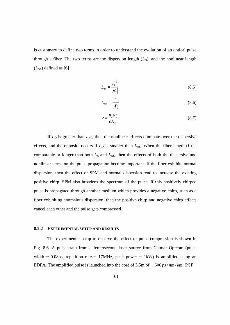
161
is customary to define two terms in order to understand the evolution of an optical pulse
through a fiber. The two terms are the dispersion length (LD), and the nonlinear length
(LNL) defined as [6]
2
20
βT
LD = (8.5)
0
1
PLNL γ
= (8.6)
effcA
n 02ωγ = (8.7)
If LD is greater than LNL, then the nonlinear effects dominate over the dispersive
effects, and the opposite occurs if LD is smaller than LNL. When the fiber length (L) is
comparable or longer than both LD and LNL, then the effects of both the dispersive and
nonlinear terms on the pulse propagation become important. If the fiber exhibits normal
dispersion, then the effect of SPM and normal dispersion tend to increase the existing
positive chirp. SPM also broadens the spectrum of the pulse. If this positively chirped
pulse is propagated through another medium which provides a negative chirp, such as a
fiber exhibiting anomalous dispersion, then the positive chirp and negative chirp effects
cancel each other and the pulse gets compressed.
8.2.2 EXPERIMENTAL SETUP AND RESULTS
The experimental setup to observe the effect of pulse compression is shown in
Fig. 8.6. A pulse train from a femtosecond laser source from Calmar Optcom (pulse
width ~ 0.08ps, repetition rate = 17MHz, peak power = 1kW) is amplified using an
EDFA. The amplified pulse is launched into the core of 3.5m of kmnmps //600− PCF

162
Fig. 8.6 Experimental setup for demonstrating pulse compression
using a manual 3-axis alignment stage. After passing through the PCF, the pulse
propagates through another length segment of single mode fiber (SMF). The pulse traces
are measured using an autocorrelator from Femtochrome, Inc which displays the pulse
trace on a laptop screen connected to it. The trace of the pulse entering the EDFA and
that exiting the SMF section after passing through the PCF are shown in Fig. 8.7. It can
be seen from the figures that the input pulse (shown in Fig. 8.7(a)) with a pulse width of
1.848ps is compressed to a width of 401.94fs after passing through the PCF (shown in
Fig. 8.7(b)). Since the chirp cancellation occurs effectively only in the linear portion
(center of the pulse), compression takes place most
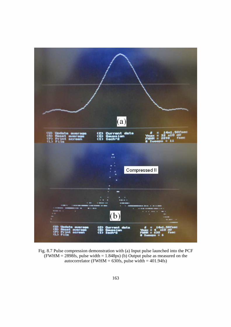
163
Fig. 8.7 Pulse compression demonstration with (a) Input pulse launched into the PCF (FWHM = 2898fs, pulse width = 1.848ps) (b) Output pulse as measured on the
autocorrelator (FWHM = 630fs, pulse width = 401.94fs)

164
efficiently in the center of the pulse [6]. This creates a characteristic pedestal wherein the
chirp cancellation is not complete.
8.3 Summary
In this chapter, the fabricated design of a highly dispersive photonic crystal fiber
was presented. This photonic crystal fiber possessed the highest dispersion coefficient
demonstrated so far. Application of highly dispersive PCF beyond its use in PAA systems
was also demonstrated. For this purpose, the PCF with the dispersion coefficient of
kmnmps //600− at 1550nm was used. A PCF-based compression system was setup and
compression of a pulse with a pulse width of 1.848ps to a pulse with a pulse width of
401.94fs was demonstrated.
8.4 References
[1] M. Y. Chen, H. Subbaraman, and R. T. Chen, “Dual-concentric-core Photonic Crystal Fiber with -5400ps/nm/km Dispersion Coefficient,” in OFC/NFOEC Technical Conference, 24-26 Mar 2009, San Diego (2009)
[2] J. C. Knight, T. A. Birks, P. St J. Russell, and D. M. Atkin, “All-silica single-mode optical fiber with photonic crystal cladding,” Opt. Letts. vol. 21, pp. 1547−1549 (1996)
[3] P. Kaiser and H. W. Astle, “Low loss single material fibers made from pure fused silica,” J. Bell Syst. Tech. vol. 53, pp. 1021−1039 (1974)
[4] A. Bjarklev, J. Broeng, and A. S. Bjarklev, Photonic crystal fibers, Kluwer Academic Publishers (2003)
[5] F. Gérôme, J. –L. Auguste, J. Maury, J. –M. Blondy, and J. Marcou, “Theoretical and Experimental Analysis of a Chromatic Dispersion Compensating Module Using a Dual Concentric Core Fiber,” J. Lightwav. Technol. vol. 24, pp. 442-228 (2006)

165
[6] G. P. Agrawal, Nonlinear Fiber Optics, Academic Press (1995)
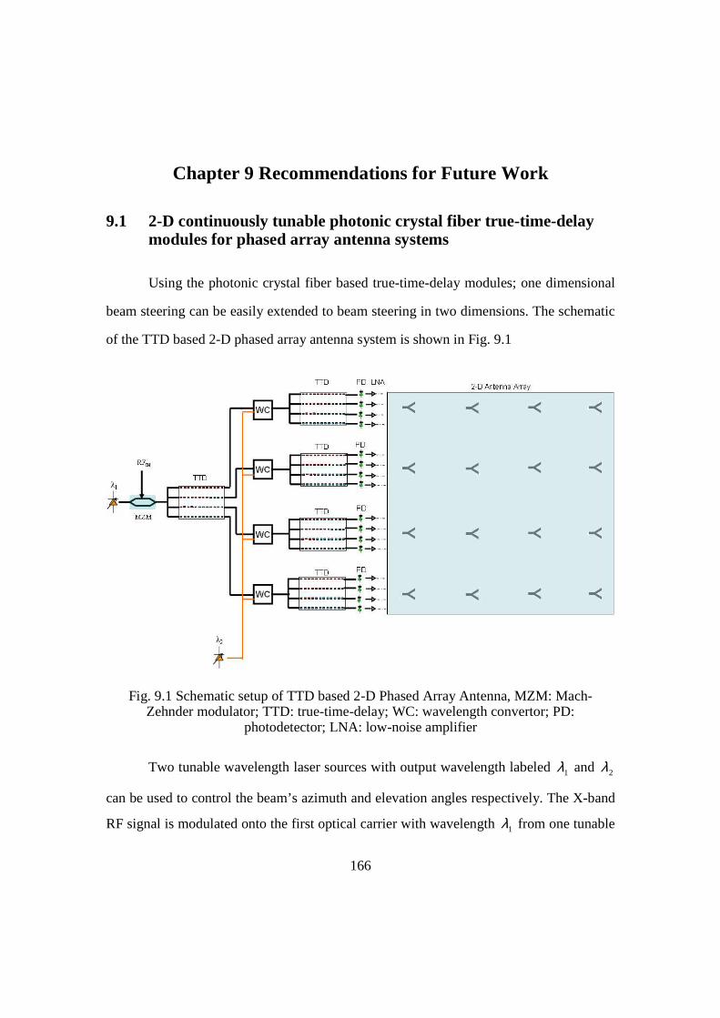
166
Chapter 9 Recommendations for Future Work
9.1 2-D continuously tunable photonic crystal fiber true-time-delay modules for phased array antenna systems
Using the photonic crystal fiber based true-time-delay modules; one dimensional
beam steering can be easily extended to beam steering in two dimensions. The schematic
of the TTD based 2-D phased array antenna system is shown in Fig. 9.1
Fig. 9.1 Schematic setup of TTD based 2-D Phased Array Antenna, MZM: Mach-Zehnder modulator; TTD: true-time-delay; WC: wavelength convertor; PD:
photodetector; LNA: low-noise amplifier
Two tunable wavelength laser sources with output wavelength labeled 1λ and 2λ
can be used to control the beam’s azimuth and elevation angles respectively. The X-band
RF signal is modulated onto the first optical carrier with wavelength 1λ from one tunable

167
laser source using a Mach-Zehner modulator. This modulated carrier is split to the TTD
lines, just as in the 1-D case. After passing through each TTD line comprising of different
lengths of PCF and NZ-DSF lines, each of the outputs is passed through a wavelength
convertor (WC). By feeding the WC with an optical carrier with wavelength 2λ from a
second tunable laser source, the phase information carrier by wavelength 1λ can be
transferred to 2λ . Each of the four outputs from the WC device is further split into 4
channels using an optical power splitter and fed to the four delay lines of four respective
TTD networks. The sixteen outputs from the four TTD modules are converted to
electrical signals using photodetectors (PD) and amplified using low-noise amplifiers
(LNA). These amplified signals feed corresponding antenna elements on a 4x4 antenna
array. Thus, by changing 1λ and 2λ , the elevation and azimuth angles of the radiated
beam can be changed continuously.
9.2 Other applications of highly dispersive PCF
Highly dispersive PCFs can be designed to achieve positive dispersion in the
wavelength range of operation. An interplay between the nonlinearity and positive
dispersion can be used to launch a pulse in the PCF that does not change its shape for a
very long distance, thus finding great application in high speed optical communications.
9.2.1 SOLITON PROPAGATION The dispersive and nonlinear lengths in a fiber are given by equations (8.5), (8.6)
and (8.7). In order for an input pulse to retain its shape, DL and NLL should be equal. By
equating equations (8.5) and (8.6) we get

168
0022
20
Pn
cATLL eff
NLD ωβ=== (9.1)
In a hollow core photonic crystal fiber, the core is made of air. Therefore, the
nonlinear refractive index coefficient is over 1000 times lower than that of silica.
Therefore, for a fixed 0T and 2β , a hollow core PCF can support 1000 times higher peak
power compared to a conventional single mode fiber. Even higher peak powers can be
supported since the effA can also be tuned in PCF.
An input pulse with a pulse width of 2.5ps is launched into one end of a 2m long
air core photonic crystal fiber from Crystal Fiber A/S (HC - 1550 - 02 ) with a dispersion
coefficient of kmnmps //100 at 1550nm and 244 mAeff µ= . The pulse from the other end
of the PCF is observed using an autocorrelator connected to a laptop. The variation in the
shape of the pulse as a function of the power of the pulse (by tuning the pump current of
the pulse source) is also measured and the results are shown in Fig. 9.2. It can be seen
that at a pump current of 110mA, the pulse output from the PCF has a width equal to the
input pulse, thus showing a soliton. By further increasing the current, second order
solitons start appearing at the output. The second order soliton can be clearly seen at a
pump current of 210mA, wherein wings at the sides are prominent. The higher order
solitons have pulse widths smaller than that of the fundamental soliton, which is also
confirmed in Fig. 9.2

169
Fig. 9.2 Measured pulse traces of soliton from the PCF at different pump current levels
Therefore, by using a hollow core PCF with a dispersion coefficient of
kmnmps //100 , a pulse with an energy of 0.1 microJoule and pulse width of 1ps, a
soliton with a peak power of 44kW can be propagated. If, on the other hand, a pulse with
an energy of 1microJoule and a pulse width of 1ps is launched into a hollow core PCF
with a dispersion coefficient of kmnmps //1000 , 0.5MW peak power soliton can be
propagated through the fiber. These results are impossible to achieve with a conventional
fiber due to the limitation of damage threshold of silica core.
9.3 Summary
In this chapter, the architecture for a 2-D phased array antenna system employing
highly dispersive photonic crystal fibers was presented. Two tunable laser sources, in

170
conjunction with wavelength convertors can be to control the elevation and azimuth
angles of the radiated RF beam. Another application of highly dispersive photonic crystal
fibers for use in soliton generation was also presented. A PCF with a dispersion
coefficient of kmnmps //100 at 1550nm was used to generate and support a soliton.
With an increase in laser pump current, higher order solitons were also generated. By
utilizing hollow core photonic crystal fibers, extremely high peak power solitons can be
propagated without damaging the fiber.
171
Chapter 10 Summary
This doctoral research focused on the design and experimental use of highly
dispersive photonic crystal fibers for use in single and simultaneous multiple RF beam
transmission and reception. RF performance of the overall system was evaluated and
other potential applications of highly dispersive photonic crystal fibers were also
explored.
Designs of highly dispersive photonic crystal fibers for both index-guiding as well
as photonic bandgap guiding PCFs showed that very high negative or positive dispersion
coefficients could be achieved by proper design. In the case of index-guiding PCF based
on dual concentric-core structure, dispersion coefficient as high as kmnmps //9500− at
1550nm with a full width at half maximum of about 55nm was obtained. Another highly
dispersive fiber with a dispersion coefficient greater than kmnmps //5400− near
1550nm was designed and fabricated. The measured dispersion coefficient is the highest
reported so far. In the case of a photonic bandgap PCF, dispersion coefficient greater than
kmnmps //4000 at 1550nm was obtained. Such highly dispersive PCF designs show
great promise in phased array antenna applications.
A true-time-delay module consisting of four delay lines was formed using the
fabricated highly dispersive PCF with a dispersion coefficient of kmnmps //600− at
1550nm and non-zero dispersion shifted fibers (NZ-DSF) such that the overall length of
each delay line was 10.5m with 3.5m length difference of PCF segments between
adjacent delay lines. The delay lines were characterized and time delays through the
delay lines as a function of wavelength were measured. The NZ-DSF sections in each
172
delay line were trimmed to produce zero time delay differences between adjacent delay
lines at a central wavelength of 1545nm.
Using the PCF-TTD based X-band phased array antenna system, single RF beam
transmission and receiving capability of the system was demonstrated first. Two RF
signals were transmitted to and received from two different directions by tuning the
wavelength on a tunable laser source. Single beam results were then extended to
demonstrate simultaneous dual beam transmission and receiving capabilities of the PAA
system by transmitting and receiving two RF beam simultaneously to/from two different
directions by simultaneously controlling the wavelengths of two tunable laser sources for
the first time. The X-band PAA system with an antenna array with inter-element spacing
= 1.3cm is capable of transmitting and receiving single or multiple RF beams from -410
to +460 by tuning the wavelength on tunable laser sources from 1530nm to 1560nm.
The noise and distortion characteristics of the PCF-TTD based PAA system were
evaluated. Noise figure (NF) and spurious-free dynamic range (SFDR) of the system with
the modulator set to operate at quadrature were measured to be 37dB and 106dB.Hz2/3
respectively at an input optical power of 20mW. Using a high power Erbium-doped fiber
amplifier (EDFA) at the input of the modulator, the NF and SFDR are improved to
23.47dB and 115dB.Hz2/3 by setting the modulator bias at 1530 and optical power to
200mW.
The feasibility of a sparse antenna array based PAA system employing highly
dispersive fibers was demonstrated by building a sparse array with 3 horn antenna
elements spaced 0.165m apart, mimicking a 29 element standard antenna array and

173
measuring the far-field radiation patterns to -30 and +30 due to PCF length limitation in
the TTD module. In order to demonstrate beam steering at larger angles, another TTD
module was constructed using dispersion compensation fibers (DCF) with a dispersion
coefficient of kmnmps //100− . Using the DCF-based sparse antenna array system, RF
beams were able to be transmitted to -450 and +450 by tuning the laser wavelength.
The fabricated photonic crystal fiber structure exhibiting the highest dispersion
coefficient reported so far was presented. This PCF exhibited a very high dispersion
coefficient of kmnmps //5400− at 1549nm and kmnmps //3900+ at 1560nm. Other
interesting applications of highly dispersive PCFs were also explored and pulse
compression effect and soliton propagation effects were demonstrated. The PCF with the
dispersion coefficient of kmnmps //600− at 1550nm was used in conjunction with an
EDFA and a femtosecond laser source to compress a 1.848ps pulse to a pulse width of
401.94fs. A hollow core PCF with a dispersion coefficient of kmnmps //100 at 1550nm
respectively was used to demonstrate soliton propagation.

174
Appendix
Publications of Harish Subbaraman
[1] M. Y. Chen, X. Lu, and Harish Subbaraman, “Conformal Ink-jet Printed C- band Phased-Array Antenna Incorporating Carbon Nanotube Field-effect Transistor Switch based True-time Delay Line,” submitted to IEEE. Trans. Antenna. Propag (2009)
[2] M. Y. Chen, X. Lu, Harish Subbaraman, and R. T. Chen, “Fully printed phased- array antenna for space communications,” in Proc. SPIE. vol. 7318, pp. 731814-1 (2009)
[3] M. Y. Chen, Harish Subbaraman, and R. T. Chen, “Dual-concentric-core Photonic Crystal Fiber with -5400ps/nm/km Dispersion Coefficient,” in OFC/NFOEC Technical Conference, 24-26 Mar 2009, San Diego (2009)
[4] Harish Subbaraman, M. Y. Chen, and R. T. Chen, “Packaging and system demonstration of an X-band phased array antenna utilizing highly dispersive photonic crystal fiber based true-time-delay,” in Proc. SPIE, vol. 7221, pp. 722107-1 (2009)
[5] Harish Subbaraman, M. Y. Chen, and R. T. Chen, “Spurious-Free Dynamic Range (SFDR) improvement in a true-time-delay system based on highly dispersive photonic crystal fiber,” in IEEE/LEOS Winter Topical Meeting Series, pp. 58-59, 12-14 Jan 2009, Innsbruck, Austria (2009)
[6] J. Vaillancourt, H. Zhang, P. Vasinajindakaw, H. Xia, X. Lu, X. Han, D. C. Janzen, W.-S. Shih, C. S. Jones, M. Stroder, M. Y. Chen, Harish Subbaraman, R. T. Chen, U. Berger, and M. Renn, “All ink-jet-printed carbon nanotube thin- film transistor on a polyimide substrate with an ultrahigh operating frequency of over 5 GHz,” Appl. Phys. Letts. vol. 93, pp. 243301 (2008)
[7] Harish Subbaraman, M. Y. Chen, and R. T. Chen, “Photonic Dual RF Beam Reception of an X-band Phased Array Antenna using Photonic Crystal Fiber based True-Time-Delay Beamformer,” Appl. Opt, vol. 47, pp. 6448-6452 (2008)
[8] Harish Subbaraman, M. Y. Chen, and Ray. T. Chen, “Photonic Crystal Fiber Based True-Time-Delay Beamformer for Multiple RF Beam Transmission and Reception of an X-Band Phased Array Antenna,” IEEE/OSA J. Lightwav. Technol. vol. 26, pp. 2803-2809 (2008)
175
[9] Harish Subbaraman, M. Y. Chen, Y. Jiang, and R. T. Chen, “Reply to Comment on Design of a broadband highly dispersive pure silica photonic crystal fiber,” Appl. Opt. vol. 44, pp. 3330-3332 (2008)
[10] M. Y. Chen, Harish Subbaraman, and R. T. Chen, “Photonic Crystal Fiber Beamformer for Multiple X-band Phased-Array Antenna Transmissions,” IEEE. Photon. Technol. Letts. vol. 5, pp. 375-377 (2008)
[11] Harish Subbaraman, M. Y. Chen, and R. T. Chen, “Simultaneous Dual RF Beam Reception of an X-Band Phased Array Antenna Utilizing Highly Dispersive Photonic Crystal Fiber Based True-Time-Delay,” AOE 2008 Technical Conference, Oct 30 - Nov 2, Shanghai, China (2008)
[12] Harish Subbaraman, T. Ling, Y. Jiang, M. Y. Chen, P. Cao, and R. T. Chen, “Design of a Broadband Highly Dispersive Pure Silica Photonic Crystal Fiber,” Appl. Opt. vol. 46, pp. 3263-3268 (2007)
[13] M. Y. Chen, Harish Subbaraman, and R. T. Chen, “Highly dispersive photonic crystal fiber for beamforming,” in Proc. SPIE. vol. 6838, 683801, (2007) (Invited Paper)
[14] Harish Subbaraman, P. Cao, M. Y. Chen, and R. T. Chen, “The Design and Fabrication of a Highly Dispersive Photonic Crystal Fiber for Phased Array Antenna Systems,” Proceedings of The OSA Topical Conference on Nanophotonics (NANO), pp. 92, Hangzhou, China, June 18-21, (2007)

176
Bibliography
Chapter 1
[1] H. J. Visser, Array and Phased Array Antenna Basics, John Wiley and Sons Ltd (2005)
[2] C. A. Balanis, Antenna theory: Analysis and design, 3rd Edition, John Wiley & Sons (2005)
[3] R. C. Hansen, Phased array antennas, Wiley-Interscience (1998)
[4] S. Barker and G. M. Rebeiz, “Distributed MEMS true-time delay phase shifters and wide-band switches,” IEEE. Trans. Microwav. Theory. Techniq. vol. 46, pp. 1881 - 1890 (1998)
[5] W. Ng, A. A. Walston, G. L. Tangonan, J. J. Lee, I. L. Newberg, and N. Bernstein, “The first demonstration of an optically steered microwave phased array antenna using true-time-delay,” IEEE. J. Lightwav. Technol. vol. 9, pp. 1124- 1131 (1991)
[6] R. D. Esman, M. Y. Frankel, J. L. Dexter, L. Goldberg, M. G. Parent, D. Stilwell, and D. G. Cooper, “Fiber-optic prism true time-delay antenna feed,” IEEE Photon. Technol. Letts. vol. 11, pp. 1347-1349 (1993)
[7] R. Soref, “Optical dispersion technique for time-delay beam steering,” Appl. Opt. vol. 31, pp. 7395-7397 (1992)
[8] Y. Chen and R. T. Chen, “A fully packaged true time delay module for a K-band phased array antenna system demonstration,” IEEE. Photon. Technol. Letts. vol. 14, pp. 1175 – 1177 (2002)
[9] S. Yegnanarayanan and B. Jalali, “Wavelength-selective true time delay for optical control of phased-array antenna,” IEEE. Photon. Technol. Letts. vol. 12, pp. 1049 – 1051 (2000)
[10] D. Dolfi, J. P. Huignard, and M. Baril, “Optically controlled true-time delays for phased array antenna,” Proc. SPIE. vol. 1102, pp. 152 (1989)
[11] D. Dolfi, F. Michel-Gabriel, S. Bann, and J. P. Huignard, “Two-dimensional optical architecture for true-time-delay beam forming in a phased-array antenna,” Opt. Letts. vol. 16, pp. 255-257 (1991)
177
[12] D. Dolfi, P. Joffre, J. Antoine, J. P. Huignard, D. Philippet, and P. Granger, “Experimental demonstration of a phased-array antenna optically controlled with phase and time delays,” Appl. Opt. vol. 35, pp. 5293-5300 (1996)
[13] N. A. Riza, “Transmit/receive time-delay beam-forming optical architecture for phased-array antennas,” Appl. Opt. vol. 30, pp. 4594-4595 (1991)
[14] N. A. Riza, “Liquid crystal-based optical time delay control system for wideband phased arrays,” Proc. SPIE. vol. 1790, pp. 171-183 (1992)
[15] A. M. Levine, “Use of fiber optic frequency and phase determining element in radar,” in Proceedings of the 33rd Annual Symposium on Frequency Control, IEEE, 436-443 (1979)
[16] P. M. Freitag and S. R. Forrest, “A coherent optically controlled phased array antenna system,” IEEE. Microwav. Guided. Wav. Letts. vol. 3, pp. 293-295 (1993)
[17] L. Xu, R. Taylor, and S. R. Forrest, “True-time delay phased array antenna feed system based on optical heterodyne techniques,” IEEE. Photon. Technol. Letts. vol. 8, pp. 160-162 (1996)
[18] D. K. T. Tong, and M. C. Wu, “A novel multiwavelength optically controlled phased array antenna with a programmable dispersion matrix,” IEEE. Photon. Technol. Letts. vol. 8, pp. 812-814 (1996)
[19] P. Goutzoulis and D. K. Davies, “Hardware-compressive 2-D fiber-optic delay line architecture for time steering of phased-array antennas,” Appl. Opt. vol. 29, pp. 5353-5359 (1990)
[20] P. Goutzoulis and D. K. Davies, “All-optical hardware-compressive wavelength multiplexed fiber optic architecture for true-time delay steering of 2-D phased array antenna,” Proc. SPIE. vol. 1703, pp. 604-614 (1992)
[21] P. Goutzoulis and D. K. Davies, J. Zomp, P. Hrycak, and A. Johnson, “Development and field demonstration of a hardware-compressive fiber-optic true time delay steering system for phased array antennas,” Appl. Opt. vol. 33, pp. 8173-8185 (1994)
[22] Z. Fu and R. T. Chen, “Highly packing density optical true-time delay lines for phased array antenna applications,” Recent Research Developments Series, pp. 1, Dec. 1998
[23] S. Yegnanarayanan, P. D. Trinh, and B. Jalali, “Recirculating photonic filter: a wavelength-selective time delay for phased array antennas and wavelength code division multiple access,” Opt. Letts. vol. 21, pp. 740-742 (1996)

178
[24] W. D. Jemison and P. R. Herczfeld, “Acousto-optically controlled true-time delay,” IEEE. Microwav. Guided Wav. Letts. vol. 3, pp. 72-75 (1993)
[25] L. H. Gesell, R. E. Feinleib, J. L. Lafuse, and T. M. Turpin, “Acousto-optic control of time delays for array beam steering,” Proc. SPIE. vol. 2155, 194 (1994)
[26] E. N. Toughlian and H. Zmuda, “A photonic variable RF delay line for phased array antennas,” IEEE. J. Lightwav. Technol. vol. 8, pp. 1824-1828 (1990)
[27] E. H. Monsay, K. C. Baldwin, and M. J. Caucuitto, “Photonic true-time delay for high-frequency phased array systems,” IEEE. Photon. Technol. Letts. vol. 6, pp. 118-120 (1994)
[28] R. D. Esman, M. J. Monsma, J. L. Dexter, and D. G. Cooper, “Microwave True Time-Delay Modulator Using Fibre-Optic Dispersion,” Electron. Letts. vol. 28, pp. 1905-1907 (1992)
[29] M. Y. Frankel and R. D. Esman, “True time-delay fiber-optic control of an ultra wideband array transmitter/receiver with multibeam capability,” IEEE. Trans. Microwav. Theory. Techniq. vol. 43, pp. 2387–2394 (1995)
[30] S. T. Johns, D. A. Norton, C. W. Keefer, R. Erdmann, and R. A. Soref, “Variable time delay of microwave signals using high dispersion fibre,” Electron. Letts. vol. 29, pp. 555-556 (1993)
[31] J. L. Cruz, B. Ortega, M. V. Andres, B. Gimeno, D. Pastor, J. Capmany, and L. Dong, “Chirped fiber gratings for phased array antenna,” Electron. Letts. vol. 33, pp. 545-546 (1997)
[32] J. L. Corral, J. Marti, S. Regidor, J. M. Fuster, R. Laming, and M. J. Cole, “Continuously variable true time-delay optical feeder for phased-array antenna employing chirped fiber gratings,” IEEE. Trans. Microwav. Theory. Techniq. vol. 45, pp. 1531-1536 (1997)
[33] Z. Shi, Y. Jiang, B. Howley, Y. Chen, F. Zhao, and R. T. Chen, "Continuously delay time tunable-waveguide hologram module for X-band phased-array antenna,” IEEE. Photon. Technol. Letts. vol. 15, pp. 972-974 (2003)
[34] Z. Shi, L. Gu, B. Howley, Y. Jiang, Q. Zhou, R. T. Chen, M. Y. Chen, X. Wang, H. R. Fetterman, and G. Brost, “True-time-delay modules based on single tunable laser in conjunction with waveguide-hologram for phased-array antenna,” Opt. Engineering. vol. 44, 084301, (2005)
[35] X. Chen, Z. Shi, L. Gu, B. Howley, Y. Jiang, and R. T. Chen, “Miniaturized Delay time-enhanced Photopolymer Waveguide Hologram Module for Phased-Array Antenna,” IEEE. Photon. Technol. Letts. vol. 17, pp. 2182-2184, (2005)

179
[36] G. P. Agrawal, Nonlinear Fiber Optics, Academic Press (1995)
[37] K. Thyagarajan, R. K. Varshney, P. Palai, A. K. Ghatak, and I. C. Goyal, “A Novel Design of a Dispersion Compensating Fiber,” IEEE. Photon. Technol. Letts. vol. 8, pp. 1510-1512 (1996)
[38] J. -L. Auguste, R. Jindal, J. -M. Blondy, M. Clapeau, J. Marcou, B. Dussardier, G. Monnom, D. B. Ostrowsky, B. P. Pal, and K. Thyagarajan, “-1800ps/(nm.km) chromatic dispersion at 1.55µm in dual concentric core fibre,” Electron. Letts. vol, pp. 1689-1690 (2000)
[39] Y. Ni, L. Zhang, L. An, J. Peng, and C. Fan, “Dual-Core Photonic Crystal Fiber for Dispersion Compensation,” IEEE. Photon. Technol. Letts. vol. 16, pp. 1516-1518 (2004).
[40] F. Gerome, J. -L. Auguste, and J. –M. Blondy, “Design of dispersion-compensating fibers based on a dual-concentric-core photonic crystal fiber,” Opt. Letts. vol. 29, pp. 2725-2727 (2004)
[41] A. Huttunen, P. Torma, “Optimization of dual-core and microstructure fiber geometried for dispersion compensation and large mode area,” Opt. Express. vol. 13, pp. 627-635 (2005)
[42] P. J. Roberts, B. J. Mangan, H. Sabert, F. Couny, T. A. Birks, J. C. Knight, and P. St. J. Russell, “Control of dispersion in photonic crystal fibers,” J. Opt. Fiber. Commun. Rep. 2, pp. 435-461 (2005)
Chapter 2
[1] [1] J. C. Knight, T. A. Birks, P. St. J. Russell, and D. M. Atkin, “All-silica single-mode optical fiber with photonic crystal cladding,” Opt Letts. vol. 21, pp. 1547-1549 (1996); Also “errata,” vol. 22, 484 (1997)
[2] J. Broeng, D. Mogilevstev, S. E. Barkou, and A. Bjarklev, “Photonic crystal fibres : A new class of optical waveguides,” Opt. Fiber. Tech. vol. 5, pp. 305-330 (1999)
[3] Bjarklev, J. Broeng, A. S. Bjarklev, Photonic crystal fibers, Kluwer Academic Publishers (2003)
[4] P. St J. Russell, "Photonic crystal fibers," Science. vol. 299, pp. 358-362 (2003)
180
[5] T. A. Birks, D. Mogilevtsev, J. C. Knight, P. St. J. Russell, “Dispersion compensation using single-material fibers,” IEEE Photon. Technol. Letts. vol. 11, pp. 674 – 676 (1999)
[6] L. P. Shen, W. P. Huang, G. X. Chen, S. S. Jian, “Design and optimization of photonic crystal fibers for broad-band dispersion compensation,” IEEE. Photon. Technol. Letts. vol. 15, pp. 540-542 (2003)
[7] A. Huttunen and P. Torma, “Optimization of dual-core and microstructure fiber geometried for dispersion compensation and large mode area,” Opt. Express. vol. 13, pp. 627-635 (2005)
[8] Y. Ni, L. Zhang, L. An, J. Peng, and C. Fan, “Dual-Core Photonic Crystal Fiber for Dispersion Compensation,” IEEE. Photon. Technol. Letts. vol. 16, pp. 1516-1518 (2004)
[9] K. Thyagarajan, R. K. Varshney, P. Palai, A. K. Ghatak, and I. C. Goyal, “A Novel Design of a Dispersion Compensating Fiber,” IEEE. Photon. Technol. Letts. vol. 8, pp. 1510-1512 (1996)
[10] J. -L. Auguste, R. Jindal, J. -M. Blondy, M. Clapeau, J. Marcou, B. Dussardier, G. Monnom, D. B. Ostrowsky, B. P. Pal, and K. Thyagarajan, “-1800ps/(nm.km) chromatic dispersion at 1.55µm in dual concentric core fibre,” Electron. Letts. vol. 36, pp. 1689-1690 (2000)
[11] F. Gérôme, J. -L. Auguste, and J. –M. Blondy, “Design of dispersion-compensating fibers based on a dual-concentric-core photonic crystal fiber,” Opt. Letts. vol. 29, pp. 2725-2727 (2004)
[12] P. J. Roberts, B. J. Mangan, H. Sabert, F. Couny, T. A. Birks, J. C. Knight, and P. St. J. Russell, “Control of dispersion in photonic crystal fibers,” J. Opt. Fiber. Commun. Rep. vol. 2, pp. 435-461 (2005)
[13] R. Amezcua-Correa, F. G´erˆome, S. G. Leon-Saval, N.G. R. Broderick, T. A. Birks, and J. C. Knight, “Control of surface modes in low loss hollow-core photonic bandgap fibers,” Opt. Express. vol. 16, pp. 1142-1149 (2008)
[14] J. D. Joannopoulos, R. D. Meade, and J. N. Winn, Photonic Crystals, Princeton University Press (1995)
[15] J. D. Joannopoulos, S. G. Johnson, J. N. Winn, and R. D. Meade, Photonic Crystals: Molding the flow of light, Princeton University press, 2nd ed. (2008)
[16] B. Jopson and A. Gnauck, “Dispersion compensation for optical fiber systems,” IEEE. Comm. Mag. vol. 33, pp. 96-102 (1995)

181
[17] T. A. Birks, J. C. Knight, and P. St J. Russell, “Endlessly single-mode photonic crystal fiber,” Opt. Letts. vol. 22, pp. 961-963 (1997)
[18] Z. Yusoff, J. H. Lee, W. Belardi, T. M. Monro, P. C. Teh, and D. J. Richardson, “ Raman effects in a highly nonlinear holey fiber: amplification and modulation,” Opt. Letts. vol. 27, pp. 424-426 (2002)
[19] K. Tajima, J. Zhou, K. Nakajima, and K. Sato, “Ultralow Loss and Long Length Photonic Crystal Fiber,” J. Lightwav. Technol. vol. 22, pp. 7-10 (2004)
[20] M. Koshiba and K. Saitoh, “Simple evaluation of confinement losses in holey fibers,” Opt. Comm. vol. 253, pp. 95-98 (2005)
[21] S. K. Varshney, K. Saitoh, and M. Koshiba, “A Novel Design for Dispersion Compensating Photonic Crystal Fiber Raman Amplifier,” IEEE. Photon. Technol. Letts. vol. 17, pp. 2062-2064 (2005)
[22] S. K. Varshney, T. Fujisawa, K. Saitoh, and M. Koshiba, “Design and analysis of a broadband dispersion compensating photonic crystal fiber Raman amplifier operating in S-band,” Opt. Express. vol. 14, pp. 3528-3540 (2006)
[23] B. J. Mangan, F. Couny, L. Farr, A. Langford, P. J. Roberts, D. P. Williams, M. Banham, M. W. Mason, D. F. Murphy, E. A. M. Brown, and H. Sabert, “Slope-matched dispersion-compensating photonic crystal fibre,” Lasers and Electro-Optics, 2004. (CLEO). (Conference on Vol. 2, 16-21 May 2004), pp. 1069-1070.
[24] U. Peschel, T. Peschel, and F. Lederer, “A compact device for highly efficient dispersion compensation in fiber transmission,” Appl. Phys. Letts. vol. 67, pp. 2111-2113 (1995)
[25] V. M. Schneider and J. A. West, “Analysis of wideband dispersion slope compensating optical fibres by supermode theory,” Electron. Letts, vol. 38, pp. 306-307 (2002)
[26] H. Subbaraman, T. Ling, Y. Q. Jiang, M. Y. Chen, P. Y. Cao, and R. T. Chen, “Design of a broadband highly dispersive pure silica photonic crystal fiber,” Appl. Opt. vol. 46, pp. 3263 – 3268 (2007)
[27] K. M. Ho, C. T. Chan, and C. M. Soukoulis, “Existence of a Photonic Gap in Periodic Dielectric Structures,” Phy. Rev. Letts. vol. 65, pp. 3152-3155 (1990)
[28] RSoft Photonics CAD Suite, Version 5.1.7
[29] R. Scarmozzino, A. Gopinath, R. Pregla, and S. Helfert, “Numerical Techniques for Modeling Guided-Wave Photonic Devices,” J. Selected Topics in Quantum Electronics. vol. 6, pp. 150-162 (2000)
182
[30] R. Scarmozzino and R. M. Osgood, Jr, “Comparison of finite-difference and Fourier-transform solutions of the parabolic wave equation with emphasis on integrated-optics applications,” J. Opt. Soc. Amer. A. vol. 8, 724-731 (1991)
[31] J. C. Knight, T. A. Birks, P. St J. Russell, and D. M. Atkin, “All-silica single-mode optical fiber with photonic crystal cladding,” Opt. Letts. vol. 21, pp. 1547−1549 (1996)
[32] P. Kaiser, and H. W. Astle, “Low loss single material fibers made from pure fused silica,” J. Bell Syst. Tech. vol. 53, pp. 1021−1039 (1974)
[33] M. van Eijkelenborg, M. Large, A. Argyros, J. Zagari, S. Manos, N. Issa, I. Bassett, S. Fleming, R. McPhedran, C. M. de Sterke, and N. A. Nicorovici, “Microstructured polymer optical fiber,” Opt. Express. vol. 9, pp. 319−317 (2001)
[34] K. Kiang, K. Frampton, T. Monro, R. Moore, J. Tucknott, D. Hevak, N. Broderick, D. Richardson, H. Rutt, “Extruded singlemode non-silica glass holey optical fibres,” Electron. Letts. vol. 38, pp. 546-547 (2002)
[35] D. C. Allan et al. Photonic crystal fibers: effective index and band gap guidance. In Photonic Crystals and Light Localization in the 21st Century (ed. C. M. Soukoulis) pp. 305−320 (Kluwer, Netherlands, 2001).
[36] R. Buczynski, “Photonic Crystal Fibers,” Acta Physica Polonica A, vol. 106, pp. 141-167 (2004)
[37] D. Pysz, R. Stepien, P. Szarniak, R. Buczynski, and T. Szoplik, “Comparing characteristics and prospects of fabrication of multicomponent photonic crystal fibers with different lattice structures,” Proc. SPIE, vol. 5576, pp. 74-80 (2004)
[38] T. Guo, S. Lou, H. Fang, and S. Jian, “Research on the fabrication of photonic crystal fiber,” Proc. SPIE. vol. 6352, 63523C (2006)
[39] H. Subbaraman, M. Yihong Chen, Y. Jiang, and R. T. Chen, “Reply to Comment on Design of a broadband highly dispersive pure silica photonic crystal fiber,” Appl. Opt. vol. 44, pp. 3330-3332 (2008)
Chapter 3
[1] Y. Jiang, B. Howley, Z. Shi, Q. Zhou, R. T. Chen, M. Y. Chen, G. Brost, C. Lee, “Dispersion-Enhanced Photonic Crystal Fiber Array for A True-Time-Delay Structured X-band Phased Array Antenna,” IEEE. Photon. Technol. Letts. vol. 17, pp. 187-189 (2005)
183
[2] Y. Jiang, Z. Shi, B. Howley, X. Chen, M. Y. Chen, and R. T. Chen, “Delay Time Enhanced Photonic Crystal Fibers Array for Wireless Communications using 2-D X-band Phased Array Antennas,” Opt. Engineering. vol. 44, (2005)
[3] U. Peschel, T. Peschel, and F. Lederer, “A compact device for highly efficient dispersion compensation in fiber transmission,” Appl. Phys. Letts. vol. 67, pp. 2111-2113 (1995)
[4] RSoft Photonics CAD Suite, Version 5.1.7
[5] K. M. Ho, C. T. Chan, and C. M. Soukoulis, “Existence of a Photonic Gap in Periodic Dielectric Structures,” Phy. Rev. Letts. vol. 65, pp. 3152-3155 (1990)
[6] Harish Subbaraman, M. Y. Chen, and R. T. Chen, Packaging and system demonstration of an X-band phased array antenna utilizing highly dispersive photonic crystal fiber based true-time-delay, in Proc. SPIE, vol. 7221, pp. 722107-1 (2009)
[7] H. Subbaraman, M. Y. Chen, and R. T. Chen, “Photonic dual RF beam reception of an X band phased array antenna using a photonic crystal fiber-based true-time-delay beamformer,” Appl. Opt. vol. 7, pp. 6448-6452 (2008)
[8] B. Howley, Z. Shi, Y. Jiang, and R. T. Chen, “Thermally tuned optical fiber for true time delay generation,” Opt. Laser Technol. vol. 37, pp. 29-32, (2004)
[9] H. Subbaraman, M. Y. Chen, and R. T. Chen, “Photonic Crystal Fiber-Based True-Time-Delay Beamformer for Multiple RF Beam Transmission and Reception of an X-Band Phased-Array Antenna,” J. Lightwav. Technol. vol. 26, pp. 2803-2809 (2008)
[10] M. Y. Chen, H. Subbaraman, and R. T. Chen, “Photonic Crystal Fiber Beamformer for Multiple X-band Phased-Array Antenna Transmissions,” IEEE. Photon. Technol. Letts. vol. 5, pp. 375-377 (2008)
Chapter 4
[1] D. Dolfi, J. P. Huignard, and M. Baril, “Optically controlled true-time delays for phased array antenna,” Proc. SPIE. vol. 1102, pp. 152 (1989)
[2] D. Dolfi, F. Michel-Gabriel, S. Bann, and J. P. Huignard, “Two-dimensional optical architecture for true-time-delay beam forming in a phased-array antenna,” Opt. Letts. vol. 16, pp. 255-257 (1991)
184
[3] D. Dolfi, P. Joffre, J. Antoine, J. P. Huignard, D. Philippet, and P. Granger, “Experimental demonstration of a phased-array antenna optically controlled with phase and time delays,” Appl. Opt. vol. 35, pp. 5293-5300 (1996)
[4] N. A. Riza, “Transmit/receive time-delay beam-forming optical architecture for phased-array antennas,” Appl. Opt. vol. 30, pp. 4594-4595 (1991)
[5] N. A. Riza, “Liquid crystal-based optical time delay control system for wideband phased arrays,” Proc. SPIE. vol. 1790, pp. 171-183 (1992)
[6] A. M. Levine, “Use of fiber optic frequency and phase determining element in radar,” in Proceedings of the 33rd Annual Symposium on Frequency Control, IEEE, 436-443 (1979)
[7] P. M. Freitag and S. R. Forrest, “A coherent optically controlled phased array antenna system,” IEEE. Microwav. Guided. Wav. Letts. vol. 3, pp. 293-295 (1993)
[8] L. Xu, R. Taylor, and S. R. Forrest, “True-time delay phased array antenna feed system based on optical heterodyne techniques,” IEEE. Photon. Technol. Letts. vol. 8, pp. 160-162 (1996)
[9] D. K. T. Tong, and M. C. Wu, “A novel multiwavelength optically controlled phased array antenna with a programmable dispersion matrix,” IEEE. Photon. Technol. Letts. vol. 8, pp. 812-814 (1996)
[10] P. Goutzoulis and D. K. Davies, “Hardware-compressive 2-D fiber-optic delay line architecture for time steering of phased-array antennas,” Appl. Opt. vol. 29, pp. 5353-5359 (1990)
[11] P. Goutzoulis and D. K. Davies, “All-optical hardware-compressive wavelength multiplexed fiber optic architecture for true-time delay steering of 2-D phased array antenna,” Proc. SPIE. vol. 1703, pp. 604-614 (1992)
[12] P. Goutzoulis and D. K. Davies, J. Zomp, P. Hrycak, and A. Johnson, “Development and field demonstration of a hardware-compressive fiber-optic true time delay steering system for phased array antennas,” Appl. Opt. vol. 33, pp. 8173-8185 (1994)
[13] Y. Chen and R. T. Chen, “A fully packaged true time delay module for a K-band phased array antenna system demonstration,” IEEE. Photon. Technol. Letts. vol. 14, pp. 1175 – 1177 (2002)
[14] Z. Fu and R. T. Chen, “Highly packing density optical true-time delay lines for phased array antenna applications,” Recent Research Developments Series, pp. 1, Dec. 1998

185
[15] S. Yegnanarayanan, P. D. Trinh, and B. Jalali, “Recirculating photonic filter: a wavelength-selective time delay for phased array antennas and wavelength code division multiple access,” Opt. Letts. vol. 21, pp. 740-742 (1996)
[16] W. D. Jemison and P. R. Herczfeld, “Acousto-optically controlled true-time delay,” IEEE. Microwav. Guided Wav. Letts. vol. 3, pp. 72-75 (1993)
[17] L. H. Gesell, R. E. Feinleib, J. L. Lafuse, and T. M. Turpin, “Acousto-optic control of time delays for array beam steering,” Proc. SPIE. vol. 2155, 194 (1994)
[18] E. N. Toughlian and H. Zmuda, “A photonic variable RF delay line for phased array antennas,” IEEE. J. Lightwav. Technol. vol. 8, pp. 1824-1828 (1990)
[19] E. H. Monsay, K. C. Baldwin, and M. J. Caucuitto, “Photonic true-time delay for high-frequency phased array systems,” IEEE. Photon. Technol. Letts. vol. 6, pp. 118-120 (1994)
[20] R. Soref, “Optical dispersion technique for time-delay beam steering,” Appl. Opt. vol. 31, pp. 7395-7397 (1992)
[21] J. L. Cruz, B. Ortega, M. V. Andres, B. Gimeno, D. Pastor, J. Capmany, and L. Dong, “Chirped fiber gratings for phased array antenna,” Electron. Letts. vol. 33, pp. 545-546 (1997)
[22] J. L. Corral, J. Marti, S. Regidor, J. M. Fuster, R. Laming, and M. J. Cole, “Continuously variable true time-delay optical feeder for phased-array antenna employing chirped fiber gratings,” IEEE. Trans. Microwav. Theory. Techniq. vol. 45, pp. 1531-1536 (1997)
[23] Z. Shi, Y. Jiang, B. Howley, Y. Chen, F. Zhao, and R. T. Chen, "Continuously delay time tunable-waveguide hologram module for X-band phased-array antenna,” IEEE. Photon. Technol. Letts. vol. 15, pp. 972-974 (2003)
[24] Z. Shi, L. Gu, B. Howley, Y. Jiang, Q. Zhou, R. T. Chen, M. Y. Chen, X. Wang, H. R. Fetterman, and G. Brost, “True-time-delay modules based on single tunable laser in conjunction with waveguide-hologram for phased-array antenna,” Opt. Engineering. vol. 44, 084301, (2005)
[25] X. Chen, Z. Shi, L. Gu, B. Howley, Y. Jiang, and R. T. Chen, “Miniaturized Delay time-enhanced Photopolymer Waveguide Hologram Module for Phased-Array Antenna,” IEEE. Photon. Technol. Letts. vol. 17, pp. 2182-2184, (2005)
[26] Harish Subbaraman, M. Y. Chen, and R. T. Chen, Packaging and system demonstration of an X-band phased array antenna utilizing highly dispersive photonic crystal fiber based true-time-delay, in Proc. SPIE, vol. 7221, pp. 722107-1 (2009)
186
[27] W. Ng, A. A. Walston, G. L. Tangonan, J. J. Lee, I. L. Newberg, and N. Bernstein, “The first demonstration of an optically steered microwave phased array antenna using true-time-delay,” IEEE. J. Lightwav. Technol. vol. 9, pp. 1124- 1131 (1991)
Chapter 5
[1] M. Y. Chen, H. Subbaraman, and R. T. Chen, “Photonic Crystal Fiber Beamformer for Multiple X-Band Phased-Array Antenna Transmissions,” IEEE. Photon. Technol. Letts. vol. 20, pp. 375-377 (2008)
[2] H. Subbaraman, M. Y. Chen, and R. T. Chen, “Photonic Crystal Fiber-Based True-Time-Delay Beamformer for Multiple RF Beam Transmission and Reception of an X-Band Phased-Array Antenna,” J. Lightwav. Technol. vol. 26, pp. 2803-2809 (2008)
[3] G. A. Koepf, “Optical processor for phased-array antenna beam formation,” Proc. SPIE. vol. 477, pp. 75–81 (1984)
[4] H. Subbaraman, M. Y. Chen, and R. T. Chen, “Photonic dual RF beam reception of an X band phased array antenna using a photonic crystal fiber-based true-time-delay beamformer,” Appl. Opt. vol. 7, pp. 6448-6452 (2008)
[5] L. H. Gesell, R. E. Feinleib, J. L. Lafuse, and T. M. Turpin, “Acousto-optic control of time delays for array beam steering,” Proc. SPIE. vol. 2155, pp. 194–204 (1994)
[6] N. A. Riza, “Liquid crystal-based optical time delay units for phased array antennas,” J. Lightwave Technol. vol. 12, pp. 1440–1447 (1994)
[7] R. Soref, “Optical dispersion technique for time-delay beam steering,” Appl. Opt. vol. 31, pp. 7395–7397 (1992)
[8] R. D. Esman, M. J. Monsma, J. L. Dexter, and D. G. Cooper, “Microwave true time-delay modulator using fibre-optic dispersion,” Electron. Letts. vol. 28, pp. 1905–1907 (1992)
[9] M. Y. Frankel, P. J. Matthews, and R. D. Esman, “Fiber optic true time steering of an ultrawideband receive array,” IEEE Trans. Microwave Theory Tech. vol. 45, pp. 1522–1526 (1997)
[10] M. Y. Frankel, R. D. Esman, and M. G. Parent, “Phased-array transmitter/receiver controlled by a true-time-delay fiberoptic beamformer,” IEEE Photonics Technol. Lett. vol. 7, pp. 1216–1218 (1995)

187
[11] A. Moloney, C. Edge, and I. Bennion, “Fiber grating time delay elements for phased array antennas,” Electron. Letts. vol. 31, pp. 1485–1486 (1995)
[12] J. E. Roman, M. Y. Frankel, P. J. Matthews, and R. D. Esman, “Time-steered array with a chirped grating beamformer,” Electron. Letts. vol. 33, pp. 652–653 (1997)
[13] Y. Jiang, Z. Shi, B. Howley, X. Chen, M. Y. Chen, and R. T. Chen, “Delay time enhanced photonic crystal fiber array for wireless communications using 2-D X-band phased-array antennas,” Opt. Engineering. vol. 44, 125001 (2005)
Chapter 6
[1] C. H. Cox, Analog Optical Links: Theory and Practice. Cambridge, U.K. Cambridge Univ. Press (2004)
[2] P. Dienes, The Taylor Series, An Introduction to the Theory of Functions of a Complex Variable, Clarendon Press, Oxford (1931), reprint: Dover, New York (1957)
[3] A. Karim and J. Devenport, “High Dynamic Range Microwave Photonic Links for RF Signal Transport and RF-IF Conversion,” J. Lightwave. Technol. 26, pp. 2718-2724 (2008)
[4] A. Karim and J. Davenport, “Noise Figure Reduction in Externally Modulated Analog Fiber-Optic Links,” IEEE. Photon. Technol. Letts. 19, pp. 312-314 (2007)
[5] G. E. Betts, J. P. Donnelly, J. N.Walpole, S. H. Groves, F. J. O’Donnell, L. J. Missaggia, R. J. Bailey, and A. Napoleone, “Semiconductor laser sources for externally modulated microwave analog links,” IEEE Trans. Microw. Theory Tech. vol. 45, pp. 1280–1287 (1997)
[6] H. Subbaraman, M. Y. Chen, and R. T. Chen, “Spurious-Free Dynamic Range (SFDR) improvement in a true-time-delay system based on highly dispersive photonic crystal fiber,” in IEEE/LEOS Winter Topical Meeting Series, pp. 58-59, Innsbruck, Austria (2009)
Chapter 7
[1] H. J. Visser, Array and Phased Array Antenna Basics, John Wiley and Sons Ltd (2005)
188
[2] Y. Liu, Z. Nie, and Q. Liu, “Reducing the number of elements in a linear antenna array by the matrix pencil method,” IEEE. Trans. Antennas. Propag. vol. 56, pp. 2955-2962 (2008)
[3] B. P. Kumar and G. R. Branner, “Design of Unequally Spaced Arrays for Performance Improvement,” IEEE. Trans. Antennas. Propag. vol. 47, pp. 511-523 (1999)
[4] R. L. Haupt, “Thinned arrays using genetic algorithms,” IEEE Trans. Antennas. Propag. vol. 42, pp. 993–999 (1994)
[5] M. G. Bray, D. H. Werner, D. W. Boeringer, and D. W. Machuga, “Optimization of thinned aperiodic linear phased arrays using genetic algorithms to reduce grating lobes during scanning,” IEEE. Trans. Antennas. Propag. vol. 50, pp. 1732–1742 (2002)
[6] T. G. Spence and D. H. Werner, “Design of Broadband Planar Arrays Based on the Optimization of Aperiodic Tilings,” IEEE. Transactions. Antennas. Propag. vol. 56, pp. 76-86 (2008)
[7] D. S. Goshi, K. M. K. H. Leong, and T. Itoh, “A Sparsely Designed Retrodirective Transponder,” IEEE. Antennas. Wireless. Propag. Letts. vol. 5, pp. 339-342 (2006)
[8] B. Howley, Z. Shi, Y. Jiang, and R. T. Chen, “Thermally tuned optical fiber for true time delay generation,” Opt. Laser Technol. vol. 37, pp. 29-32 (2004)
Chapter 8
[1] M. Y. Chen, H. Subbaraman, and R. T. Chen, “Dual-concentric-core Photonic Crystal Fiber with -5400ps/nm/km Dispersion Coefficient,” in OFC/NFOEC Technical Conference, 24-26 Mar 2009, San Diego (2009)
[2] J. C. Knight, T. A. Birks, P. St J. Russell, and D. M. Atkin, “All-silica single-mode optical fiber with photonic crystal cladding,” Opt. Letts. vol. 21, pp. 1547−1549 (1996)
[3] P. Kaiser and H. W. Astle, “Low loss single material fibers made from pure fused silica,” J. Bell Syst. Tech. vol. 53, pp. 1021−1039 (1974)
[4] Bjarklev, J. Broeng, A. S. Bjarklev, Photonic crystal fibers, Kluwer Academic Publishers (2003)
[5] F. Gérôme, J. –L. Auguste, J. Maury, J. –M. Blondy, and J. Marcou, “Theoretical and Experimental Analysis of a Chromatic Dispersion Compensating Module

189
Using a Dual Concentric Core Fiber,” J. Lightwav. Technol. vol. 24, pp. 442-228 (2006)
[6] G. P. Agrawal, Nonlinear Fiber Optics, Academic Press (1995)
190
Vita
Harish Subbaraman was born in Hyderabad, India on October 13, 1982. He is the
son of Subbaraman Sundaresan and Dr. Anuradha Raman. He received the Bachelor of
Engineering degree in Electronics and Communication Engineering from Chaitanya
Bharathi Institute of Technology, India. He entered the graduate school at The University
of Texas at Austin in 2004 and earned the degree of Master of Science in Engineering
from Department of Electrical and Computer Engineering in 2006.
Permanent address: 1399, Street 20, Nagarjuna Nagar
Tarnaka, Secunderabad,
Andhra Pradesh, India.
500017
This dissertation was typed by the author