control system of steel battery charger
TRANSCRIPT
FACTA UNIVERSITATIS
Series: Automatic Control and Robotics Vol. 16, No 3, 2017, pp. 241 - 252
https://doi.org/10.22190/FUACR1703241D
CONTROL SYSTEM OF STEEL BATTERY CHARGER
UDC ((621.3.077.5+621.43.044.7):681.518.52)
Nikola Danković1
, Dragan Antić1,
Zoran Icić1, Stanko Stankov
1, Dejan Mitić
1, Marko Živković
2
1University of Niš, Faculty of Electronic Engineering, Department of Control Systems,
Niš, Republic of Serbia 2University of Niš, University Computer Center, Niš, Republic of Serbia
Abstract. A practical realization of control of a diode–thyristor bridge is provided in
this paper. The proposed control logic is applied to an NiCd accumulator charger.
These accumulators are used for power supply of electrical devices and equipment in
CFR locomotives. The control system provides a regular mode of NiCd accumulators
charging and discharging, and, in this way, their long lifespan. A hardware
configuration and a control algorithm for efficient NiCd accumulator charging and
preventing overcharging and overheating are provided.
Key words: steel accumulator, charger, control logic, thyristor, ignition angle
1. INTRODUCTION
Steel (NiCd) batteries are reliable sources of electricity and they have various good
performances: long lifespan, wide range of operating temperatures, resistance to mechanic
and electric loads, high discharge currents. These batteries also do not generate corrosive
gasses, they are can be recharged rapidly, and they are very easy for maintenance. It has
been shown that this type of batteries retain service performances even during a multiyear
storage without electrolyte and for the electricity empty state. From the aspect of
environmental protection NiCd batteries are a green source of energy because 99% metal
for construction of batteries can be recycled [1].
Steel (NiCd) batteries are widely used in the systems with required permanent power
supply (diesel and electrical locomotives, motor trains, trams, trolleybuses, etc.).
Accumulators with lamellar electrodes [2] are usually used in such systems. A typical
characteristic of KPL series accumulators (low discharge rate cells) is shown in Fig. 1. The
nominal voltage of the battery (operating voltage) is 1.2 V. The nominal capacity of the
Received September 10, 2017
Corresponding author: Nikola Danković
Faculty of Electronic Engineering, Aleksandra Medvedeva 14, 18000 Niš, Republic of Serbia
E-mail: [email protected]

242 N. DANKOVIĆ, D. ANTIĆ, Z. ICIĆ, S. STANKOV, D. MITIĆ, M. ŽIVKOVIĆ
battery is the five-hour capacity (C5) at the temperature 20 ± 5°C. Nominal charge/discharge
current is: I=0.2 C5A.
Fig. 1 Typical discharge characteristic of KPL accumulators at 20⁰C
Accumulator performances (lifetime, good battery usage, and operational readiness)
mostly depend on a charging strategy and the rectifier–accumulator–receiver system. The
simplest way is on/off charge and discharge of accumulators. A charger is usually a diode
rectifier where the consumer is off during charging and the charger is off when the
consumer is connected. A more efficient system is obtained when the controlled charger is
inserted between the accumulator and the consumer [3].
A block diagram of the controlled charger (rectifier) of an NiCd accumulator is shown
in Fig. 2. A power supply of a consumer within a locomotive (lighting, heating system,
ventilation, air condition, communication, etc.) consists of a diode–thyristor bridge, an
accumulator, a control unit, and an LCD module.
A rectifier is used for charging, monitoring, and keeping an NiCd accumulator in a
charged state, and also for power supply of DC consumers at CFR type of electrical
locomotives. An accumulator consists of 84 1.2V voltage units connected in series.
Voltage regulation is in the range of 100V up to 126V, and current regulation is in the
range of 7A up to 20A. The power supply of a diode–thyristor unit is led from the
locomotive generator, i.e. from AC1, AC2 connectors. For one semi-period the thyristor
TH1 and the diode D2 are conductive, and for another semi period the thyristor TH2 and
the diode D1 are conductive [3]. A regulation circuit holds a constant output voltage of
the thyristor unit by adjusting the thyristor ignition angle. The above mentioned voltage
and current ranges can be extended from 0 up to 250V and from 0 to 20A, respectively,
by an appropriate power supply and choice of components of the diode–thyristor bridge.
The LCD modules for monitoring of the set and current values of current and voltage are
connected with control unit via an RS232 communication.

Control System of Steal Battery Charger 243
C1 R1
TH1
a c
C1 R1
TH2
b d
C2 R2
D1
C2 R2
D2
AV
a
b
c
d
1
2
3
s
s
L
Rsh
F
R LOAD
- +-
TxRxGNDVcc+24VDC
Tx Rx GND Vcc +24VDC
LCD MODULE
CONTROL UNIT
THYRISTOR MODULE
100 ÷ 126 V
Rs
1
2
L
AC1 AC2
+--
BATTERIES 84*1,2V
V~
V~
AGND
Io
L
2*16 CHARACTERS
Fig. 2 A block diagram of charging an NiCd accumulator in the locomotive
2. THE CONTROL SYSTEM OF AN NICD ACCUMULATOR CHARGER
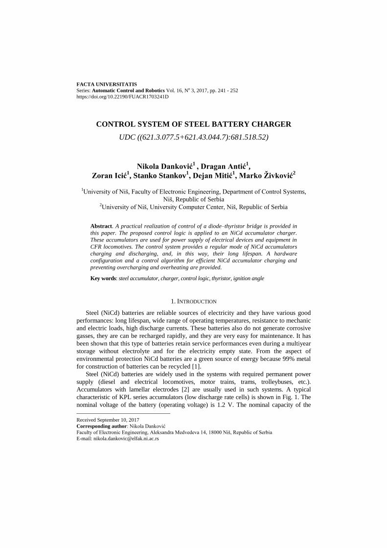
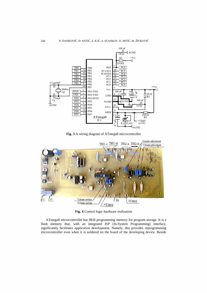
Rectifier control is performed by using ATmega8 microcontroller. A scheme of this
controller is given in Fig. 3, and hardware realization in Fig. 4. It is a cheap component
with ˝hardware concept˝ and AVR RISC architecture designed in CMOS technology, and
it is well-known for its low consumption [4].
244 N. DANKOVIĆ, D. ANTIĆ, Z. ICIĆ, S. STANKOV, D. MITIĆ, M. ŽIVKOVIĆ
PB0 RES
PB1PB2PB3PB4PB5
PC5/SCLPC4/SDA
PC3PC2PC1PC0PB6
PB7
PD1/TXD
PD1/TXD
PD2/INTO
PD3
PD4
PD5
PD6
PD7
Vcc
GND
AGND
AVcc
AREF
ATmega8IC1
+++
+++
1
PB1
PB2
PB3
PB4
PB5
PC6
C8
100 nF
AGND
2
1516171819
3
4
5
6
11
12
13
RXD
TXD
PD2
PD3
PD4
PD5
PD6
PD7
7
8
22
20
21
C34
.7 µ
F
C1
PB0
10pF
10pF
8MHzQ1
C5
C6
AGND
910
AGND
+VREF
AGND
+Vcc
282726252423
PC3PC2PC1PC0
PC4PC5
10 k
R1 +Vcc
R210
250 R3
4.7
µF
C4100 nF
GND
TL431IC2 (2.5V)
C2
100 nF
Fig. 3 A wiring diagram of ATmega8 microcontroller
Fig. 4 Control logic hardware realization
ATmega8 microcontroller has 8KB programming memory for program storage. It is a
flash memory that, with an integrated ISP (In-System Programming) interface,
significantly facilitates application development. Namely, this provides reprogramming
microcontroller even when it is soldered on the board of the developing device. Beside

Control System of Steal Battery Charger 245
programming the memory, the microcontroller has 1KB static RAM memory for data
storage, and 512B EEPROM memory whose role is to store data that must not be lost
when there is no voltage supply. Programming FLASH memory is organized as 4K*16
bits, because commands at the AVR microcontroller are 16 or 32 B. The Pipeline
mechanism, which allows downloading the next instruction during the execution of the
previous one, is integrated, as well. The concept of the RISC architecture and pipeline
mechanism provides that each instruction is executed in one interval of the system tact.
An important characteristic of an AVR microcontroller is that frequencies of a tact and
oscillator, used for generating pulses, are equal. It means that the ATmega8 processor on
16MHz has a speed of 16 MIPS, which is very good for 8-bit processors [4, 5].
AVR microcontrollers have 32 8-bit registers of general purpose. Each register can be
used as an accumulator in executing arithmetic operations, wherein there are some
restrictions of usage of certain registers for some instructions. Registers are mapped in
SRAM memory at first 32 addresses. At next 64 addresses the I/O registers of peripheral
microcontroller units are mapped. Intern SRAM memory starts from address 60H.
ATmega8 microcontroller has three I/O ports: port B with eight derived pins on the
processor case, port C with seven pins, and port D with eight pins. Each pin has
multiplexed additional functions depending on which the peripheral unit is used. For
example, on port C pins, analogue inputs of A/D convertor are located.
Pins can be configured as either input or output, independently of how other pins of
the same port are configured. Pins PB1, PB0 trigger optothyristors TH1.1 and TH1.2, and
galvanic separated pulses are sent in this way (Fig. 5).
R1390 k
PB1
R347 1W
a
c
R222 k
TLP541
R5390 k
R747 1W
b
d
R622 k
TLP541
L
R8100 1W
R4100 1W
A
K
G
A
K
G
TH1-1
TO ENERGETIC MODULETH1-2
PB0
Fig. 5 Galvanic isolated signals for thyristor ignition in the rectifier

246 N. DANKOVIĆ, D. ANTIĆ, Z. ICIĆ, S. STANKOV, D. MITIĆ, M. ŽIVKOVIĆ
Optothyristors open gates of energetic thyristor TH1, TH2 of a diode–thyristor bridge
are shown in Fig. 2.
Power supply with zero-crossing detection of control unit and following electronics is
taken from a voltage source given in Fig. 6 [4].
PC0GND
BDX33C
GN
DVin Vout
7824
C5
35
V1000 µ
F
+ C6
100 n
FDC/DC
24/±5V
+
+
F10.5A
F20.5A
AC1
GR1
AC2
4*1N 4007
C1
100 nF250 V
R1100 1W
Var
C235 V
R22,2 k1W
47 µF
1N4007
ZPD30V
C3
35
V1000 µ
F
+ C4
100 n
F
C7+
C8+
+Vcc
-Vee
GND
470µ
F470µ
F
100 kR3
10 kR4
ZPD5,1V
Fig. 6 A scheme for rectifier power supply
This is a classical configuration with diodes, serial transistor, stabilized integrated
source 7824, integrated DC/DC converter, and a certain number of passive components.
A voltage oscillogram on the rectifier output, in the case of resistor load, is shown in
Fig. 7. Voltage level depends on the thyristor ignition angle.
Fig. 7 Wave form of the rectifier voltage output
Control System of Steal Battery Charger 247
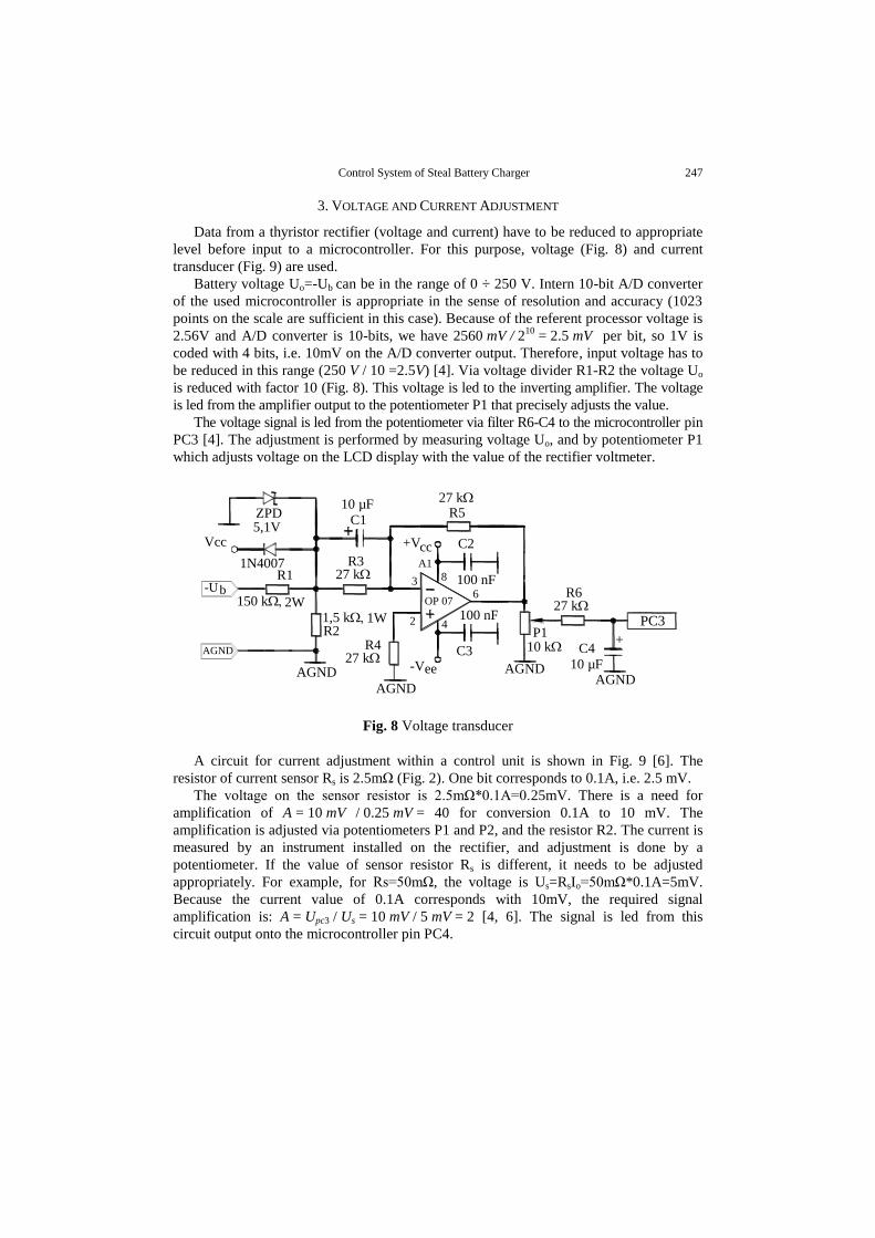
3. VOLTAGE AND CURRENT ADJUSTMENT
Data from a thyristor rectifier (voltage and current) have to be reduced to appropriate
level before input to a microcontroller. For this purpose, voltage (Fig. 8) and current
transducer (Fig. 9) are used.
Battery voltage Uo=-Ub can be in the range of 0 ÷ 250 V. Intern 10-bit A/D converter
of the used microcontroller is appropriate in the sense of resolution and accuracy (1023
points on the scale are sufficient in this case). Because of the referent processor voltage is
2.56V and A/D converter is 10-bits, we have 2560 mV / 210
= 2.5 mV per bit, so 1V is
coded with 4 bits, i.e. 10mV on the A/D converter output. Therefore, input voltage has to
be reduced in this range (250 V / 10 =2.5V) [4]. Via voltage divider R1-R2 the voltage Uo
is reduced with factor 10 (Fig. 8). This voltage is led to the inverting amplifier. The voltage
is led from the amplifier output to the potentiometer P1 that precisely adjusts the value.
The voltage signal is led from the potentiometer via filter R6-C4 to the microcontroller pin
PC3 [4]. The adjustment is performed by measuring voltage Uo, and by potentiometer P1
which adjusts voltage on the LCD display with the value of the rectifier voltmeter.
+V cc C2
C3
100 nF
100 nF
-Vee
3
2
6
8
4
R427 k
A1
OP 07
+
10 µF
C4
R627 k
R527 k
R327 k
C1
10 µF
R1
150 k 2Wb
R21,5 k 1W PC3
P110 k
ZPD5,1V
1N4007
Vcc
AGND
AGNDAGND
AGND
AGND
-U
Fig. 8 Voltage transducer
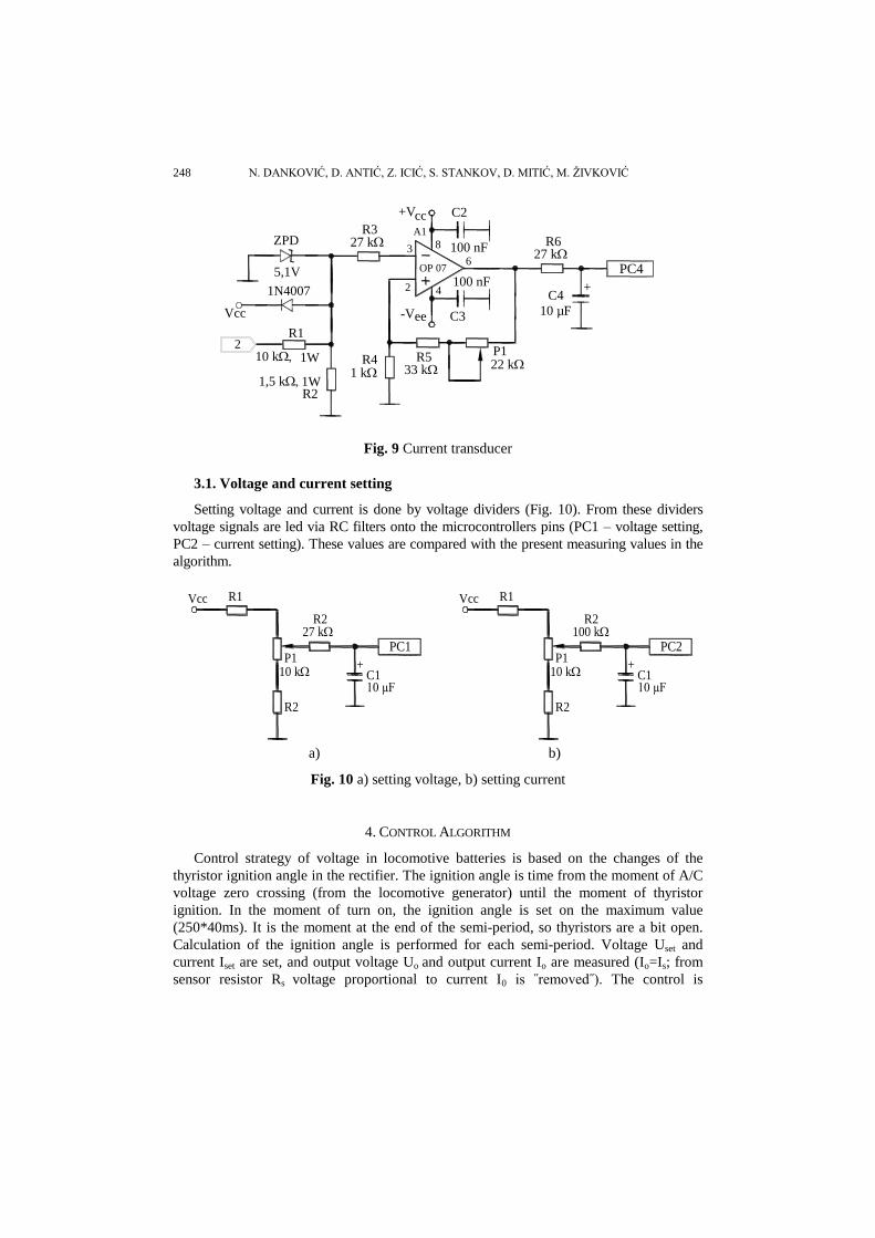
A circuit for current adjustment within a control unit is shown in Fig. 9 [6]. The
resistor of current sensor Rs is 2.5mΩ (Fig. 2). One bit corresponds to 0.1A, i.e. 2.5 mV.
The voltage on the sensor resistor is 2.5mΩ*0.1A=0.25mV. There is a need for
amplification of A = 10 mV / 0.25 mV = 40 for conversion 0.1A to 10 mV. The
amplification is adjusted via potentiometers P1 and P2, and the resistor R2. The current is
measured by an instrument installed on the rectifier, and adjustment is done by a
potentiometer. If the value of sensor resistor Rs is different, it needs to be adjusted
appropriately. For example, for Rs=50mΩ, the voltage is Us=RsIo=50mΩ*0.1A=5mV.
Because the current value of 0.1A corresponds with 10mV, the required signal
amplification is: A = Upc3 / Us = 10 mV / 5 mV = 2 [4, 6]. The signal is led from this
circuit output onto the microcontroller pin PC4.
248 N. DANKOVIĆ, D. ANTIĆ, Z. ICIĆ, S. STANKOV, D. MITIĆ, M. ŽIVKOVIĆ
+V cc C2
C3
100 nF
100 nF
-Vee
3
2
6
8
4
R41 k
A1
OP 07
+
10 µF
C4
R627 k
R327 k
R1
10 k 1W2
R21,5 k 1W
PC4
ZPD
5,1V
1N4007
Vcc
R533 k
P122 k
Fig. 9 Current transducer
3.1. Voltage and current setting
Setting voltage and current is done by voltage dividers (Fig. 10). From these dividers
voltage signals are led via RC filters onto the microcontrollers pins (PC1 – voltage setting,
PC2 – current setting). These values are compared with the present measuring values in the
algorithm.
+
10 µFC1
R227 k
PC1P1
10 k
R2
R1Vcc
+
10 µFC1
R2100 k
PC2P1
10 k
R2
R1Vcc
a) b)
Fig. 10 a) setting voltage, b) setting current
4. CONTROL ALGORITHM
Control strategy of voltage in locomotive batteries is based on the changes of the
thyristor ignition angle in the rectifier. The ignition angle is time from the moment of A/C
voltage zero crossing (from the locomotive generator) until the moment of thyristor
ignition. In the moment of turn on, the ignition angle is set on the maximum value
(250*40ms). It is the moment at the end of the semi-period, so thyristors are a bit open.
Calculation of the ignition angle is performed for each semi-period. Voltage Uset and
current Iset are set, and output voltage Uo and output current Io are measured (Io=Is; from
sensor resistor Rs voltage proportional to current I0 is ˝removed˝). The control is

Control System of Steal Battery Charger 249
performed based on the set and measured values: if output current I0 is less than set Iset
and voltage Uo is less than Uset, the program reduces the thyristor ignition angle for 1 bit
(40µs). This angle is constant for the next two semi-periods (n=2). After n semi-periods
the ignition angle is again calculated in the previously described way. When Uo=Uset, Iset>Io the microprocessor increases the ignition angle for 1 bit. In this way the output
voltage is decreased. If in the next iteration Uo<Uset the ignition angle is decreased for 1
bit to increase voltage. In this way, the output voltage Uo is oscillating within the range
1V around the set value. If Io>Iset then the ignition angle is increased for 1 bit that causes
decreasing voltage. The procedure is continued until Io≤Iset. Then, the condition Uo≤Uset is
checked, and if it is valid, the ignition angle is decreased for 1 bit that causes increasing
voltage. In the next moment, if Io>Iset the ignition angle is increased for 1 bit, etc. In the
case, when there is no voltage in the thyristor (control unit), the control circuit decreases
the ignition angle (maximal openness of a thyristor) to increase voltage. If in this moment
maximal voltage level is reached, the control logic has a role to reduce it to the set level.
This voltage reduction is performed in the following procedure: if Uset>0, Uo=0, Io=0, the
ignition angle α>50 (the condition when there is no rectifier voltage), the processor sets a
certain value for the ignition angle (e.g. 200*40μs) instead of the minimum value. If there
is a voltage on thyristors, the control is performed by the described algorithm. The wave
forms of output rectifier voltage and current for resistance and battery load are given,
respectively in Figs. 11, 12, and 13.
Fig. 11 Oscillogram of voltage and current for resistance load
a) voltage on the load (minimum) b) load current
Fig. 12 Oscillogram of voltage and current for resistance load
a) voltage on the load (minimal ignition angle) b) load current

250 N. DANKOVIĆ, D. ANTIĆ, Z. ICIĆ, S. STANKOV, D. MITIĆ, M. ŽIVKOVIĆ
Fig. 13 Oscillogram of voltage and current for battery load
a) voltage on the load b) load current
5. DISPLAYING SET AND MEASURED VALUES
Displaying characteristic variables and parameters is provided via an LCD monitor
(2*16 characters) with an integrated controller and DDRAM (Display Data Random
Access Memory) with capacity of 80B (memory for 80 characters). CGRAM (Character
Generator Random Access Memory) of 64B provides defining 8 characters in the form of
5*8 pixel matrixes. CGROM (Character Generator Read Only Memory) includes predefined
characters of 8320 bits. Display has a backlight. Hardware realization is shown in Fig. 14.
Fig. 14 LCD display hardware realization
An LCD module (Fig. 15) can communicate via 8-bit or 4-bit data bus depending on
sending certain functional instructions during initialization. In the case of 8-bit Data
Interface, data transfer is done at once via pins DB0 ÷ DB7. In the case of 4-bit Data
Interface, data transfer is performed in two steps via pins DB4 ÷ DB7; firstly upper and
then lower nibble is transferred. At the moment of turning on the voltage supply the LCD
module automatically starts initialization process by an intern reset circuit. An LCD
controller has 11 instructions which are actually combinations of bits on RS, R/W, and
LCD data bus pins, when Enable pin on the level of a logic unit.
Control System of Steal Battery Charger 251
1 R21200 Vcc
10 k
2.2 k
BC 337T1
Vcc
GND
10 k GND
GND
2 3 4 5 6 7 8 9 10 11 12 14 15
PC
5
PC
4
PB
0
PB
1
PB
2
PB
3
PB
4
PB
5
PD
6
PD
7
P
2*16 CHARACTERS LCD MODULE
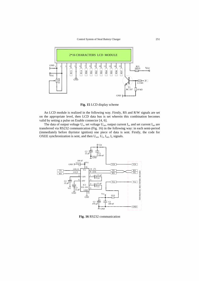
Fig. 15 LCD display scheme
An LCD module is realized in the following way. Firstly, RS and R/W signals are set
on the appropriate level, then LCD data bus is set wherein this combination becomes
valid by setting a pulse on Enable connector [4, 6].
The data of output voltage Uo, set voltage Uset, output current Io, and set current Iset are
transferred via RS232 communication (Fig. 16) in the following way: in each semi-period
(immediately before thyristor ignition) one piece of data is sent. Firstly, the code for
OXEE synchronization is sent, and then Uset, Uo, Iset, Io signals.
Vcc
+10V
16
-10V
2
6
IC3
ICL 232
GND
GND
Vcc100 nF
GND
Vcc
TH
YR
IST
OR
R
EC
TIF
IER
B
OA
RD
V24
RXTX
GND
C222 µF
+
V24
TX
RX
C322 µF
TX
RX22 µF
22 µF
C4
C5
+
+
1
8 (13)
14 (7)
3
4
5
(12) 9
(10) 12
C1
15
+
C222 µF
+
GND
C2100 nF
V24
C2470 µF
+
GND
C2100 nF
Vcc10
VccVcc
GND
Fig. 16 RS232 communication

252 N. DANKOVIĆ, D. ANTIĆ, Z. ICIĆ, S. STANKOV, D. MITIĆ, M. ŽIVKOVIĆ
6. CONCLUSION
In this paper, a regulation of a thyristor charger for NiCd accumulators that have wide
range of applications (in this case CFR-type locomotive), is presented. The advantages of
these accumulators are high reliability, long lifespan, temperature, mechanical and electrical
stability, and easy maintenance. The control system is based on ATmega8 microcontroller.
The control algorithm consists of measuring output current and voltage, and of comparing
the obtained values with the ones set in advance. On the basis of this, the ignition angle is
calculated. An integrated LCD display gives set and measured values of the current and
voltage.
The control algorithm given in this paper was proved in practical realization as good
enough. However, in some future work, it could be improved with some intelligent
control as fuzzy logic or neural networks.
Acknowledgement: This paper was realized as a part of the projects "Studying climate change and
its influence on the environment: impacts, adaptation and mitigation" (III 43007), and "Research and
Development of New Generation Wind Turbines of High-energy Efficiency" (TR 35005), financed by
the Ministry of Education and Science of the Republic of Serbia within the framework of integrated
and interdisciplinary research for the period 2011-2018.
REFERENCES
[1] D. Linden, T. B. Ready, Handbook of batteries, McGraw-Hill, New York, 2002.
[2] S. Newman, K. E. Thomas-Alyea, Electrochemical Systems, 3rd ed., Englewood Cliffs: Prentice-Hall,
2004.
[3] R. Bernd, Maintenance-Free Batteries, 3rd ed., Overseas Press India, New Delhi, 2010.
[4] S. Stankov, Z. Icić, S. Nikolić, "Sawmill control device," in Proceedings of 23th International conf.
process industry, Procesing, Tara, Serbia, pp. 151-158, 2010, (in Serbian).
[5] C. Kuhnel, AVR RISC Microcontroller Handbook, 1st ed., Newnes, 1998.
[6] H. Zumbahlen, Linear Circuit Design Handbook, Newnes/Elsevier, 2008.