continuous‑time delta‑sigma modulator in advanced digital
TRANSCRIPT
This document is downloaded from DR‑NTU (https://dr.ntu.edu.sg)Nanyang Technological University, Singapore.
Continuous‑time delta‑sigma modulator inadvanced digital CMOS process
Qiu, Xiaobo
2011
Qiu, X. (2011). Continuous‑time delta‑sigma modulator in advanced digital CMOS process.Master’s thesis, Nanyang Technological University, Singapore.
https://hdl.handle.net/10356/43569
https://doi.org/10.32657/10356/43569
Downloaded on 25 Mar 2022 18:12:39 SGT

I
Continuous-Time Delta-Sigma Modulator in Advanced
Digital CMOS Process
QIU XIAOBO
SCHOOL OF ELECTRICAL AND ELECTRONIC
ENGINNERING
2011
Con
tinu
ou
s-Tim
e Delta
-Sig
ma M
od
ula
tor in
Ad
van
ced D
igita
l
CM
OS
Pro
cess
2011
QIU
XIA
OB
O

Continuous-Time Delta-Sigma Modulator in Advanced
Digital CMOS Process
QIU XIAOBO
SCHOOL OF ELECTRICAL AND ELECTRONIC ENGINNERING
2011
3
Continuous-Time Delta-Sigma Modulator in Advanced
Digital CMOS Process
QIU XIAOBO
SCHOOL OF ELECTRICAL AND ELECTRONIC ENGINNERING
A thesis submitted to the Nanyang Technological University
In fulfillment of requirement for the degree of
Master of Engineering
2011

Statement of Originality
I hereby certify that the work embodied in this thesis is the result of
original research and has not been submitted for a higher degree to any
other University or Institution.
…………………. ………………….
Date QIU XIAOBO

I
Acknowledgments
This project would not have been possible without the collaboration and support from
many individuals.
Most importantly, I would like to express my appreciation to my supervisor,
Prof. Siek Liter, for his indefatigable encouragement, inspiring and edificatory
supervision and guidance throughout the whole research process.
I would like to extend my gratitude to Prof. Tiew Kei Tee, for generously
sharing his precious knowledge and expertise in the field of analog-to-digital
data convertor design.
Special thank goes to GLOBALFOUNDRIES (formally known as Chartered
Semiconductor Manufacturing), without whose technical and financial support,
the completeness of this project will be impossible.
I would also be very grateful to my friends, Leow Yoon Hwee, Teh Li Lian,
Zhang Fan, He Jin and Trans Xuan Ann in CICS. They have shared their fun
and experience with me from time to time. I would also like to thank them for
their technical discussions.
Finally, I would also like to give my sincere appreciation to the technical staffs
in CICS lab for all their helping hands giving to me.

II
Abstract
The rapid development of fast digital signal processors implemented in
Complementary metal-oxide-semiconductor (CMOS) very-large-scale integration
(VLSI) technology has dramatically increased the demand for high speed and high
resolution analog-to-digital converters (ADCs). These ADCs can be integrated in the
fabrication technologies and optimized for digital circuit and systems. As the scaling of
the VLSI technology also severely constrains the available dynamic range for the
interface of the analog and digital signals, the ADCs are the bottleneck in most of the
mixed-signal designs. One of the ADC architectures, delta-sigma oversampling ADCs
realize an optimum tradeoff between circuit complexity, cost, and power dissipation.
High accuracy is achieved with low precision analog components.
Delta-sigma modulators with continuous-time (CT) loop filters have become more and
more popular due to some advantages over their discrete-time (DT) counterparts.
Compared with DT delta-sigma modulators, CT delta-sigma modulators are faster,
consume less power, and do not require sample-and-hold front-ends and anti-aliasing
filters. As a result, the CT delta-sigma modulators are more suitable for
telecommunication applications, which require wideband, high accuracy and high
sampling rate ADCs.
In this report, the design of a continuous-time delta-sigma ADC targeting at dynamic
range of 60dB is discussed in detail. The working principles of delta-sigma
oversampling ADCs are presented. The advantages of delta-sigma oversampling
architecture over other types are also shown based on the deviation of formulas. Some
system level simulations in MATLAB are performed to determine the block
coefficients, which are used in the circuit level design in Cadence environment. Some
nonidealities of the blocks are also modeled in MATLAB for improvement. The design
of integrator is shown in detail and the circuits for other components, such as the
multi-bit quantizer, the multi-bit feedback digital-to-analog converter (DAC), are also
discussed.
III
Table of Contents
List of Figures ......................................................................................................... VI
List of Tables ....................................................................................................... VIII
Chapter 1 Introduction ............................................................................................ 1
1.1 Background ....................................................................................................................... 1
1.2 Motivation ......................................................................................................................... 3
1.3 Objective ........................................................................................................................... 4
1.4 Report Organization ........................................................................................................... 5
Chapter 2 Literature Review ................................................................................... 7
2.1 Delta-Sigma Modulator Fundamentals................................................................................ 7
2.1.1 General Operation.......................................................................................................... 8
2.1.2 Oversampling Technique................................................................................................ 9
2.1.3 Noise Shaping Concept ................................................................................................ 12
2.2 Design Architectures ........................................................................................................ 14
2.2.1 High-Order Delta-Sigma Modulator ............................................................................. 15
2.2.2 Multi-Stage Delta-Sigma Modulator............................................................................. 17
2.2.3 Multi-Bit Delta-Sigma Modulator ................................................................................ 19
2.3 Continuous-time Delta-Sigma Modulator ......................................................................... 20
2.3.1 Introduction to Continuous-Time Delta-Sigma Modulator ............................................ 21
2.3.2 Comparison between DT and CT Delta-Sigma Modulator ............................................ 22
2.3.2.1 Modulator Implementation .................................................................................. 22
2.3.2.2 Operation Speed .................................................................................................. 23
2.3.2.3 Anti-aliasing Filter Requirement .......................................................................... 23
2.3.2.4 Power Consumption ............................................................................................ 23
2.3.2.5 Loop Filter Scalability with Clock Frequency ...................................................... 24
2.3.3 DT-to-CT Conversion of Delta-Sigma Modulators ........................................................ 24
2.3.4 Review of Prior Works ................................................................................................. 27
2.4 Summary of Chapter 2 ..................................................................................................... 31
Chapter 3 System Level Design ..............................................................................33
3.1 Modulator Topology ........................................................................................................ 33
3.1.1 System Level Parameters ............................................................................................. 33
3.1.2 Loop Filter Architecture ............................................................................................... 36

IV
3.1.2.1 CIFF versus CIFB Structure ................................................................................ 36
3.1.2.2 Excess Loop Delay Impact ......................................................................................... 39
3.1.3 Loop Filter Coefficient Assignment .............................................................................. 44
3.1.4 Coefficient Scaling ...................................................................................................... 48
3.2 Nonidealities in Continuous-Time Delta-Sigma Modulators .............................................. 52
3.2.1 Integrator Nonidealities................................................................................................ 53
3.2.1.1 Finite Integrator DC Gain .................................................................................... 55
3.2.1.2 Finite Gain Bandwidth Product (GBW) of Op Amp.............................................. 58
3.2.2 Clock Jitter Effect ........................................................................................................ 62
3.2.3 DAC Non-linearity ...................................................................................................... 66
3.2.4 Summary of Nonidealities ............................................................................................ 70
3.3 Summary of Chapter 3 ..................................................................................................... 72
Chapter 4 Circuit Implementation .........................................................................75
4.1 Top Level Circuit ............................................................................................................. 75
4.2 RC-Integrator Design ....................................................................................................... 78
4.2.1 The Op Amp in the RC-Integrator ................................................................................ 78
4.2.2 Common-Mode Feedback (CMFB) Circuit................................................................... 81
4.2.3 Op Amp Simulation Results ......................................................................................... 83
4.3 GmC-Integrator Design .................................................................................................... 85
4.3.1 The Transconductor in the GmC-Integrator .................................................................. 85
4.3.2 Transconductor Simulation Results .............................................................................. 89
4.3.3 Other GmC-Integrators ................................................................................................ 91
4.4 Summing Circuit Design .................................................................................................. 93
4.5 Multi-bit Quantizer Design............................................................................................... 96
4.5.1 Comparator Kick-back effect ....................................................................................... 98
4.5.2 Clock Feed-Through Effect .......................................................................................... 99
4.5.3 Comparator Offset ..................................................................................................... 101
4.5.4 Comparator performance ........................................................................................... 102
4.6 Feedback DAC Design ................................................................................................... 104
4.7 D Flip-Flop (DFF) ......................................................................................................... 106
4.8 Summary of Chapter 4 ................................................................................................... 109
Chapter 5 Results and Discussions ....................................................................... 112
5.1 Circuit Level Simulation Results .................................................................................... 112
5.2 Modulator Performance Summary .................................................................................. 117

V
Chapter 6 Conclusions .......................................................................................... 119
6.1 Conclusions ...................................................................................................................... 119
6.2 Future works ..................................................................................................................... 121
Publications ........................................................................................................... 123
References .............................................................................................................. 123
Appendix A ............................................................................................................ 132

VI
List of Figures
Figure 2. 1 Block diagram of a first-order single-bit delta-sigma modulator ........................................ 8
Figure 2. 2 Frequency spectrum of (a) Nyquist-rate sampling (b) Oversampling ADC ....................... 10
Figure 2. 3 (a) Quantizer voltage transfer curve (b) quantization error function of the quantizer......... 11
Figure 2. 4 In-band quantization noise power comparison between Nyquist-rate ADCs and
oversampling ADCs .......................................................................................................................... 12
Figure 2. 5 Linearized model for 1st-order delta-sigma modulator ..................................................... 13
Figure 2. 6 Linearized model of a second-order delta-sigma modulator ............................................. 16
Figure 2. 7 A second-order modulator formed by cascading two first-order delta-sigma modulators ... 18
Figure 2. 8 Block diagram for a continuous-time delta-sigma oversampling ADC ............................. 21
Figure 2. 9 Block Diagram for a (a) DT delta-sigma modulator (b) CT delta-sigma modulator........... 25
Figure 2. 10 Feedback signal path of the (a) DT delta-sigma modulator (b) CT delta-sigma modulator
........................................................................................................................................................ 26
Figure 3. 1 Maximum out-of-band gain versus peak SNR and overload level .................................... 36
Figure 3. 2 Frequency response of the STF of a fifth-order CIFF modulator ...................................... 38
Figure 3. 3 Frequency response of the STF of a fifth-order CIFF modulator with peak removed ........ 39
Figure 3. 4 Impulse response of NRZ DAC feedback pulse (a) ideal (b) delayed ............................... 40
Figure 3. 5 Impulse response of RZ DAC feedback pulse (a) ideal (b) delayed .................................. 40
Figure 3. 6 Impulse response of HRZ DAC feedback pulse (a) ideal (b) delayed ............................... 41
Figure 3. 7 Peak SNR and input level plots versus excess loop delay................................................. 42
Figure 3. 8 PSD plots for the modulator output with ELD of 0, 0.16Ts and 0.2Ts ............................... 43
Figure 3. 9 CT modulator with additional feedback path to alleviate excess loop delay effect ............ 44
Figure 3. 10 Pole and zero plot of the synthesized DT NTF............................................................... 45
Figure 3. 11 Frequency responses of transfer functions ..................................................................... 47
Figure 3. 12 SNR plot versus input amplitude ................................................................................... 48
Figure 3. 13 Integrator outputs of un-scaled integrators ..................................................................... 49
Figure 3. 14 (a) Blocks before coefficient scaling (b) blocks after coefficient scaling......................... 50
Figure 3. 15 Internal states maximum values plot after scaling .......................................................... 51
Figure 3. 16 Integrator outputs of scaled integrators .......................................................................... 52
Figure 3. 17 SNR versus input level plot comparisons between both sets of coefficients .................... 52
Figure 3. 18 Simplified schematic for fully differential (a) RC-integrator (b) GmC-integrator ........... 53
Figure 3. 19 Single-end models for (a) RC-integrator with finite DC gain (b) GmC-integrator with finite
output resistance ............................................................................................................................... 56
Figure 3. 20 SNDR plot versus DC gain of (a) first and second integrator (b) third to fifth integrator . 57
Figure 3. 21 An n-input RC integrator .............................................................................................. 59
Figure 3. 22 First stage of the CT delta-sigma modulator with the nonideal model for RC integrator . 60
Figure 3. 23 Equivalent model for the first stage of the CT delta-sigma modulator ............................ 61
Figure 3. 24 SNDR versus GBW plot with input at -2dB of full scale................................................ 61
Figure 3. 25 Single-bit NRZ, RZ and HRZ DAC pulses with clock jitter effect ................................. 63

VII
Figure 3. 26 Multi-bit NRZ, RZ and HRZ DAC pulses with clock jitter effect ................................... 63
Figure 3. 27 SNDR versus clock jitter plot at -2dB full scale input .................................................... 66
Figure 3. 28 Delta-sigma modulator model for DAC element mismatch error .................................... 67
Figure 3. 29 Illustration of DWA ...................................................................................................... 68
Figure 3. 30 PSD plot for DAC pulses .............................................................................................. 69
Figure 3. 31 SNR versus full dynamic range ..................................................................................... 71
Figure 3. 32 PSD plot for modulators ............................................................................................... 71
Figure 4. 1 Top-level circuit block diagram ...................................................................................... 77
Figure 4. 2 RC-integrator Op Amp topology ..................................................................................... 79
Figure 4. 3 Common-mode feedback circuit topology ....................................................................... 82
Figure 4. 4 Op Amp AC response plot .............................................................................................. 84
Figure 4. 5 Op Amp phase margin .................................................................................................... 84
Figure 4. 6 Op Amp characteristic voltage-transfer-curve .................................................................. 85
Figure 4. 7 GmC-Integrator transconductor topology ........................................................................ 86
Figure 4. 8 Transconductor AC response plot .................................................................................... 90
Figure 4. 9 Transconductor phase margin ......................................................................................... 90
Figure 4. 10 Transconductor characteristic voltage-transfer-curve ..................................................... 91
Figure 4. 11 Summing circuit topology ............................................................................................. 94
Figure 4. 12 General structure of a comparator ................................................................................. 96
Figure 4. 13 Latched comparator structure ........................................................................................ 97
Figure 4. 14 feed-through effects from the parasitic capacitance........................................................ 99
Figure 4. 15 Regenerative node output signals with clock feed-through effect ................................. 100
Figure 4. 16 New comparator topology to solve the clock feed-through problem ............................. 100
Figure 4. 17 Regenerative node output signals with clock feed-through effect reduced .................... 101
Figure 4. 18 Comparator offset measurement .................................................................................. 102
Figure 4. 19 Comparator output with input pulses ........................................................................... 103
Figure 4. 20 Comparator output with differential sinusoidal input signal ......................................... 103
Figure 4. 21 Current steering NRZ DAC topology .......................................................................... 105
Figure 4. 22 D flip-flop topology .................................................................................................... 107
Figure 4. 23 DFF output with square wave input signal................................................................... 107
Figure 4. 24 Simplified clock generator .......................................................................................... 108
Figure 4. 25 Clock signal waveforms.............................................................................................. 109
Figure 5. 1 Modulator circuit topology by cascading all the block components ................................ 113
Figure 5. 2 Modulator low-frequency performance ......................................................................... 114
Figure 5. 3 Modulator high-frequency performance ........................................................................ 114
Figure 5. 4 Modulator low-frequency PSD plot .............................................................................. 115
Figure 5. 5 Modulator high-frequency PSD plot ............................................................................. 116

VIII
List of Tables
Table 2. 1 Summary of CT delta-sigma modulator performance from year 2006 to year 2009 ............ 28
Table 3. 1 Block Coefficients before Dynamic Scaling ...................................................................... 47
Table 3. 2 Block Coefficients after Dynamic Scaling......................................................................... 51
Table 3. 3 Minimum DC gain requirements of integrators ................................................................. 58
Table 3.4 Nonidealities summary ...................................................................................................... 70
Table 4. 1 Design specifications for GmC-integrators and transconductors ........................................ 92
Table 4. 2 Integration capacitances for each stage ............................................................................. 93
Table 5. 1 Modulator performance summary with low-frequency input ........................................... 117
Table 5. 2 Performance comparison between reported designs and this delta-sigma modulator......... 118

1
Chapter 1
Introduction
1.1 Background
The real world signal is analog by nature. However, it is always desirable to convert the
analog signals to the digital domain to make use of the robust, flexible and reliable
digital signal processing. Some applications of the analog to digital conversion are wide
dynamic range digital audio, radar signal processing systems, digital time-base
correction and digital enhancement of images. Due to the advancement in CMOS VLSI
technology, the digital signal processing becomes more powerful, and hence results in a
stronger need for high resolution, high speed analog-to-digital converter (ADC). There
are various kinds of ADCs that provide different ranges of resolution and speed. One of
the ADC architectures, the delta-sigma oversampling ADC, gains more and more
attention in recent years because of its relaxed requirement on the analog circuit
components. It‟s one of the favorable options in VLSI systems. The most significant
advantage of the delta-sigma ADC is its low sensitivity to the nonidealities of the
building blocks; whereas conventional ADCs show high sensitivity to the circuit
imperfections or at least need correction mechanisms. This advantage is due to the post
digital signal processing of the delta-sigma architecture, which is very favorable in
VLSI systems, because the dense and fast signal processing can be better realized in

2
digital domain than in analog circuits.
The delta-sigma technology was invented by Culter in 1960 and first published by
Inose and Yasuda in 1962 [1]. However, this technology didn‟t break through until the
integrated switch capacitor and filter implementation became common and well
understood twenty years later. After then, the easy mapping of the modulator
mathematics onto circuit level became possible. The tremendous application of the
delta-sigma modulator began after the paper on the implementation of the double
integration modulator published by Candy in 1985 [2]. At that time, the development
on delta-sigma technology was mostly on discrete-time (DT) domain.
The developments in communication industry have continuously pushed the
conversion bandwidth higher. However, the respectively long settling time of the DT
delta-sigma modulator limited the sampling frequency, and the signal bandwidth was
constrained in a rather narrow region consequently. Therefore, architecture alternatives
were necessary for further applications. As a result, the continuous-time (CT)
delta-sigma modulator became popular in the mid 1990s. In CT implementations, the
loop filters are built of continuous-time circuits such as transconductors or integrators.
The sampling frequency can be boosted up to gigahertz (GHz). Generally speaking,
most of the advantages of the CT delta-sigma ADC over its DT counterpart come from
the displacement of the sampler inside the modulator loop, which provides an implicit
anti-aliasing filter and eliminates the use of precise sample-and-hold circuit.

3
1.2 Motivation
Thanks to the development of CMOS VLSI technology, the digital signal processing is
becoming more and more powerful. Due to the increasing digital processing speed in
the Digital Signal Processor (DSP), the IEEE 802.11e standard was developed to meet
the demand for wireless transfer of large amount of data over a short distance.
According to these standards, data is transferred in a channel bandwidth of 20 MHz by
applying orthogonal frequency-division multiplexing (OFDM) modulation [3]. It is
reasonable to believe that the signal bandwidth of the next generation wireless
applications will be higher than the current one, for example, two to three times of the
current one. Therefore, requirements for high-speed building blocks are raised. One of
the key blocks in the front-end of the Wireless Local Area Network (WLAN) receiver is
the ADC. The challenge to build a high resolution, high speed ADC makes it a
bottleneck of many circuit designs.
Comparing to other types of ADCs, delta-sigma oversampling ADCs are preferred for
this application because they provide the most economic speed-accuracy tradeoff for
signal bandwidths up to 50 MHz [4]. Due to the stringent requirement on amplifier
bandwidth, discrete-time delta-sigma ADCs are less suitable for high-speed
applications. While for continuous-time implementation, besides the possible higher
sampling rates, it provides additional benefits: no sample-and-hold circuit in front, an
inherent anti-aliasing filter and low thermal noise generated by the filter circuits. Even

4
though it suffers more from excess loop delay and clock jitter problems, solutions have
already been proposed [5-6].
Multi-bit continuous-time delta-sigma ADCs are even more suitable for broadband
communications. The internal multi-bit quantizer reduces both the over sampling ratio
(OSR) and the clock jitter effect. What‟s more, the modulator stability is also improved.
The disadvantage of the multi-bit delta-sigma ADC is the presence of a less linear
multi-bit DAC in the feedback path. However, this problem can be solved by the
Dynamic Element Matching (DEM) or digital calibration method as discussed [7].
1.3 Objective
In view of the foregoing, the increasing demand of the multi-bit CT delta-sigma ADC
stimulates this project.
The project is conceived to study the working principles of delta-sigma modulators and
design a low-pass multi-bit CT delta-sigma ADC for next generation wireless
communications. The target signal band width of this modulator is 50MHz, which is
approximately two times of the current one and predicted to be necessary for next
generation wireless communication [3]. Multi-bit quantizer is used in the ADC to
reduce the oversampling ratio and improve the system stability. The modulator should
achieve dynamic range of 60dB and effective number of bits (ENOB) of around 10bits.
Assuming that the other specifications of the receiver do not alter much from previous

5
generations, the resolution of this modulator is adequate for application. The power
consumption of the modulator is restricted to be lower than 25mW. The modulator
system level design is performed in MATLAB and the transistor level design is carried
out in Cadence Virtuoso Custom Design Platform. ST Microelectronics 65nm CMOS
process is used and the supply voltage is 1.2V. This CT delta-sigma ADC will be a
good candidate for next generation wireless communications.
1.4 Report Organization
The subsequent chapters report the research study carried out within the past two years.
The report is organized in the following way.
Chapter 2 provides detailed descriptions of the delta-sigma oversampling modulator
working principle and the derivations of the formulas for quantization noise and
signal-to-noise ratio (SNR). The continuous-time implementation of the modulator and
the comparison to the discrete-time counterpart are discussed. The method for
DT-to-CT conversion is also introduced. A general review of the previous works on the
CT delta-sigma modulator is presented as well.
Chapter 3 focuses on the system level synthesis. The modulator architecture is selected
to make it more immune to the block nonidealities. The block coefficients are also
determined for the circuit implementation. The nonidealities of various blocks are
properly modeled and methods are proposed to reduce these effects.

6
Chapter 4 presents the circuit level designs of various components. The circuits are
designed to satisfy the system level requirements. Some design challenges are also
elaborated.
Chapter 5 presents the final results and discussions of this project. The comparisons
between the circuit level and system level simulation results are also included.
Chapter 6 concludes the report and recommendations for future work are given.
7
Chapter 2
Literature Review
In this chapter, basic background knowledge of delta-sigma modulators is introduced to
make the rest of the thesis easily understood. The concepts of oversampling and
noise-shaping are illustrated in detail. The comparison between DT and CT delta-sigma
analog-to-digital converters (ADCs) are also presented.
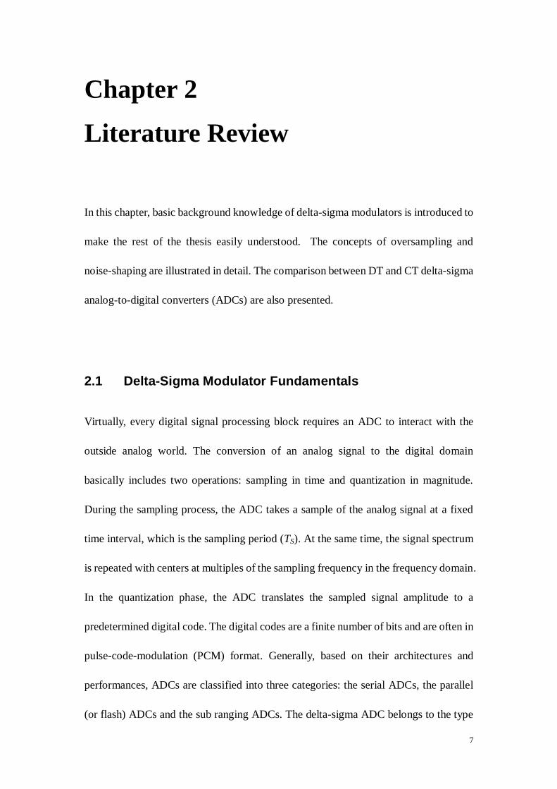
2.1 Delta-Sigma Modulator Fundamentals
Virtually, every digital signal processing block requires an ADC to interact with the
outside analog world. The conversion of an analog signal to the digital domain
basically includes two operations: sampling in time and quantization in magnitude.
During the sampling process, the ADC takes a sample of the analog signal at a fixed
time interval, which is the sampling period (TS). At the same time, the signal spectrum
is repeated with centers at multiples of the sampling frequency in the frequency domain.
In the quantization phase, the ADC translates the sampled signal amplitude to a
predetermined digital code. The digital codes are a finite number of bits and are often in
pulse-code-modulation (PCM) format. Generally, based on their architectures and
performances, ADCs are classified into three categories: the serial ADCs, the parallel
(or flash) ADCs and the sub ranging ADCs. The delta-sigma ADC belongs to the type

8
of serial ADCs, because only one output is generated in each clock cycle. In the
following sections, detailed descriptions of the delta-sigma modulator are given.
2.1.1 General Operation
The block diagram of a first-order single-bit delta-sigma modulator is shown in Figure
2.1. The delta-sigma ADC consists of an integrator, a comparator (quantizer) and a
feedback digital-to-analog converter (DAC). The closed loop forces the DAC output,
which is the estimation of the input signal, to be equal to the actual sampled analog
input. The difference between the real input signal and estimated value is the input to
the integrator. The output from the integrator is sent to the comparator, which is used as
a one-bit quantizer and operates at the sampling rate. The digital output from the
quantizer is fed into the digital decimator, which consists of a low pass filter and a down
sampler. The digital decimator converts the quantizer output into a high-resolution
digital signal at a lower speed. The speed is approximately twice of the highest signal
frequency. The design of the digital decimator is not included in this project. The
working principles of the delta-sigma architecture are discussed in the following
sections.
Figure 2. 1 Block diagram of a first-order single-bit delta-sigma modulator
Low Pass
Filter
↓D
DAC
__
Integrator Comparator Analog Input

9
2.1.2 Oversampling Technique
For Nyquist-rate converters, the sampling frequencies (fS) are usually around twice of
the signal bandwidth (fb). The sampling effect in the frequency domain is shown in
Figure 2.2(a). As shown in this figure, the signal spectrum is repeated close to each
other with centers at the integer multiples of the sampling frequency. For these ADCs,
the input signal bandwidth must be restricted within half of the sampling frequency;
otherwise interferences between the repeated signal spectra will occur. Therefore, for
Nyquist-rate ADCs, anti-aliasing filters with sharp cut-off at the signal bandwidth
should be added before the sample-and-hold (S/H) circuits. However, a filter with sharp
cut-off is quite difficult to implement in reality. Fortunately, the oversampling
technique relaxes the requirement on the anti-aliasing filter. The sampling frequency of
the oversampling ADC is much higher than that of the Nyquist-rate one. The frequency
spectrum of the input signal after oversampling is shown in Figure 2.2(b). As shown in
this figure, the repeated versions of the signal spectrum are separated far away from
each other. Hence the anti-aliasing filter is not required to be so accurate and can even
be omitted in some designs. This is one of the reasons for the expanding applications of
delta-sigma oversampling ADCs.
fb fs 2fs
f 0
Nyquist-rate sampling
fs=2fb
(a)

10
Figure 2. 2 Frequency spectrum of (a) Nyquist-rate sampling (b) Oversampling ADC
The relaxed requirement on the anti-aliasing filter is one of the advantages from the
oversampling technique. Another benefit is the reduced in-band quantization noise
power. After passing through the quantizer, the analog signal is converted to digital
codes, as shown in Figure 2.3(a). The difference between the analog signal and the
quantized output is referred to as the quantization error (Q), as depicted in Figure 2.3(b).
The maximum absolute value for the quantization error is δ/2, where δ stands for the
quantization step size, which is also named the Least Significant Bit (LSB). The
expression for δ is given by Equation (2.1).
(2.1)
where VFull-scale is the full-scale amplitude of the input signal and N stands for the
number of internal quantizer bits. Assuming that the quantization error is uniformly
distributed from -δ/2 to +δ/2, the average quantization noise power ( ) is derived as
shown by Equation (2.2).
(2.2)
fb fs 2fs
f 0
Oversampling
fs>>2fb
(b)

11
From the derivation procedure, it is obvious that the quantization noise power is
independent of the sampling frequency.
(a) (b)
Figure 2. 3 (a) Quantizer voltage transfer curve (b) quantization error function of the quantizer
Generally, the quantization noise is assumed to be a white noise and the noise power is
evenly distributed between –fS/2 and +fS/2 in the frequency domain. As a result, the
quantization noise power falling in the signal band (fb), or the so-called in-band
quantization noise power, is described by Equation (2.3).
(2.3)
where M=fS/(2fb) and stands for the oversampling ratio (OSR). From this equation, for
a specified signal bandwidth, the in-band quantization noise power will be reduced by
half if the sampling frequency is doubled. The signal-to-noise ratio (SNR) will increase
by 3dB consequently.
For Nyquist-rate ADCs, the sampling frequency fS is approximately twice of fb.
Therefore, M equals to one and all the quantization noise power falls in the signal band.

12
While for oversampling ADCs, the sampling frequency is much larger than the
Nyquist-rate. Hence M is much bigger than one and the in-band quantization noise
power is reduced a lot. The comparison of the two ADCs is shown in Figure 2.4.
Figure 2. 4 In-band quantization noise power comparison between Nyquist-rate ADCs and
oversampling ADCs
In summary, the oversampling ADC not only relaxes the accuracy requirement on the
anti-aliasing filter, but also reduces the in-band quantization noise power and increases
the SNR consequently.
2.1.3 Noise Shaping Concept
Besides the use of the oversampling technique, another special property of the
delta-sigma modulator is the noise shaping capability. Due to the delta-sigma algorithm,
the quantization noise power is pushed away from the signal band, and the SNR is
improved as a result. To analyze this property, it is helpful to use the linearized model
for the delta-sigma modulator. The linearized model for a first-order delta-sigma
modulator is shown in Figure 2.5.
Nyquist-Rate
Oversampled
fb=fs1/2 fs2/2 f
Quantization Noise

13
Figure 2. 5 Linearized model for 1st-order delta-sigma modulator
In this model, X stands for the sampled analog input and Y for the digital output. The
integrator is represented by the transfer function
and acts as an accumulator. The
added signal E stands for the quantization noise which is introduced in the quantization
process. Since the DAC just estimates the input signal, there is no actual symbol to
represent it. Using this model, the transfer function for the output signal Y is derived as
shown by Equation (2.4).
(2.4)
From this equation, it is obvious that the quantization noise pass through a network with
the transfer function , which actually represents a high-pass filter. Therefore,
the output signal is the sum of the delayed input and the high-pass filtered quantization
noise. The in-band quantization noise power is given by the following equation.
(2.5)
Comparing Equation (2.5) with Equation (2.3), it is obvious that, the in-band
quantization noise power of the delta-sigma architecture is reduced even more than that
of the oversampling ADC without the noise shaping capability. The maximum SNR
1
1
1
z
z
X
E
Y
__

14
achievable for a first-order delta-sigma ADC is shown by Equation (2.6).
(2.6)
where N stands for the number of the internal quantizer bits and , where M is the
oversampling ratio. According to this equation, if the sampling frequency of the
first-order delta-sigma modulator is doubled, the SNR will increase by 9dB and the
effective number of bits will increase by 1.5 bits.
In conclusion, comparing to the ADC using the oversampling technique only, the
delta-sigma oversampling ADC reduces the in-band quantization noise power even
more, and increases the SNR further.
2.2 Design Architectures
As explained in the above sections, for the same input signal, the SNR of a delta-sigma
oversampling modulator is much better than that of a Nyquist-rate one. However, the
resolution provided by a first-order single-bit discrete-time (DT) delta-sigma
modulator is still not high enough, even for normal audio operation, as proven by the
following example. For a CD audio with good quality, the desired resolution is 16bits,
corresponding to the SNR of 98dB. Using Equation (2.6) for a first-order delta-sigma
modulator with 1-bit internal quantizer, the required oversampling frequency is 96.78

15
MHz if the signal bandwidth is 20 kHz. In nowadays CMOS technology, the 1-bit
quantizer can operate at 96.78MHz. However, it‟s difficult for the switched-capacitor
integrators, based on which the DT delta-sigma modulators are built, to operate at such
a high speed. As a result, some other design architectures must be investigated to ensure
the high speed performance of the delta-sigma oversampling ADCs [8]. In the
following sections, some optional design architectures are described, such as the
high-order delta-sigma modulator, the multi-stage delta-sigma modulator and the
multi-bit delta-sigma modulator.
2.2.1 High-Order Delta-Sigma Modulator
In high-order delta-sigma ADCs, more than one integrators are cascaded in the
modulators to provide more suppression on the in-band quantization. Figure 2.6 shows
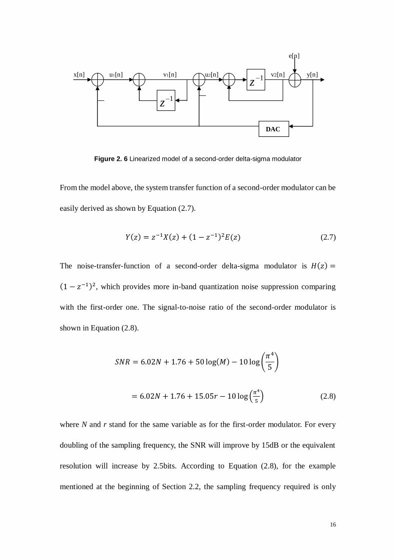
the linearized model of a second-order delta-sigma modulator. As shown in this figure,
two integrators are cascaded. The output from the first integrator, subtracted by the
DAC output, is the input to the second integrator. The second integrator input can be
treated as a more fined version of the modulator error. Thus the integrated version of the
“fined error” is quantized by the comparator. Consequently, the output is more accurate
than that of a first-order one.
16
Figure 2. 6 Linearized model of a second-order delta-sigma modulator
From the model above, the system transfer function of a second-order modulator can be
easily derived as shown by Equation (2.7).
(2.7)
The noise-transfer-function of a second-order delta-sigma modulator is
, which provides more in-band quantization noise suppression comparing
with the first-order one. The signal-to-noise ratio of the second-order modulator is
shown in Equation (2.8).
(2.8)
where N and r stand for the same variable as for the first-order modulator. For every
doubling of the sampling frequency, the SNR will improve by 15dB or the equivalent
resolution will increase by 2.5bits. According to Equation (2.8), for the example
mentioned at the beginning of Section 2.2, the sampling frequency required is only
1z
1z
DAC
x[n] y[n]
e[n]
u1[n] v1[n] u2[n] v2[n]
__ __

17
about 6.12MHz, which is much lower than that needed for the first-order one.
A second-order delta-sigma modulator consists of two integrators, thus a third-order
one consists of three integrators and so on. The peak SNR achievable for an Lth
-order
delta-sigma modulator is given by Equation (2.9).
(2.9)
where N and r stand for the same variable as for the first and second-order modulators.
Therefore, the higher the modulator order, the lower the oversampling frequency is
required to achieve the same resolution. However, the stability issue is always a
problem for high-order modulators due to the unbounded signal accumulation at the
integrator output. To solve this problem, multi-stage and multi-bit sigma-delta
modulators are usually used as substitutions.
2.2.2 Multi-Stage Delta-Sigma Modulator
High-order noise-transfer-function can also be realized by cascading several low-order
delta-sigma modulators, which are usually referred to as multi-stage noise shaping
(MASH). In this manner, the stability problem of the high-order modulator
architectures can be avoided. A second-order modulator generated by cascading two
first-order modulators is shown in Figure 2.7.
18
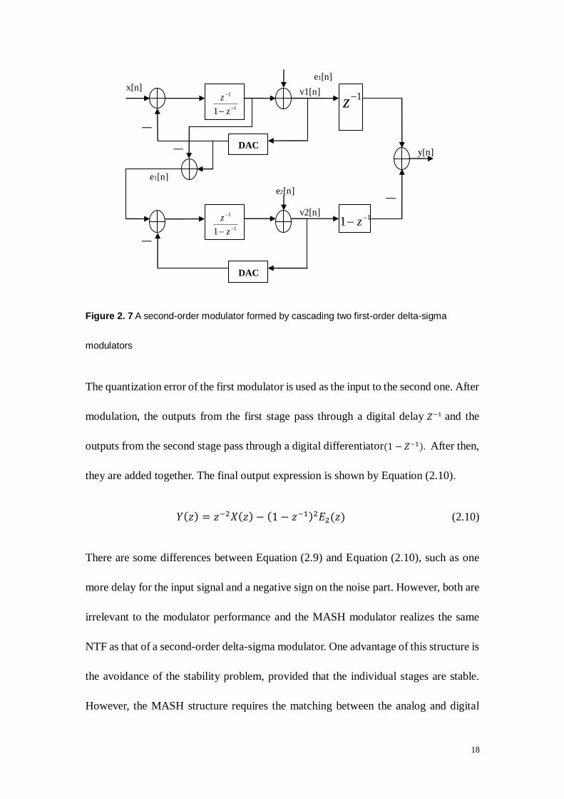
Figure 2. 7 A second-order modulator formed by cascading two first-order delta-sigma
modulators
The quantization error of the first modulator is used as the input to the second one. After
modulation, the outputs from the first stage pass through a digital delay and the
outputs from the second stage pass through a digital differentiator . After then,
they are added together. The final output expression is shown by Equation (2.10).
(2.10)
There are some differences between Equation (2.9) and Equation (2.10), such as one
more delay for the input signal and a negative sign on the noise part. However, both are
irrelevant to the modulator performance and the MASH modulator realizes the same
NTF as that of a second-order delta-sigma modulator. One advantage of this structure is
the avoidance of the stability problem, provided that the individual stages are stable.
However, the MASH structure requires the matching between the analog and digital
1z
DAC
x[n] v1[n]
1
1
1
z
z
__
__
__ y[n]
e1[n]
1
1
1
z
z
11 z
DAC
e2[n]
__
v2[n]
e1[n]

19
transfer functions as well as the matching among the DAC output levels from different
stages. Otherwise, mismatches may lead to the leakage of unshaped or poorly shaped
noise from an earlier stage. The problem of noise leakage in the continuous-time
MASH modulators is more serious than that in the discrete-time counterparts, because
the accuracy of the CT analog transfer function depends on the absolute RC time
constant, which is more difficult to control than the ratio of the capacitors. As a result,
single-stage structure is more popular in the CT delta-sigma modulator
implementations.
2.2.3 Multi-Bit Delta-Sigma Modulator
As stated in Section 2.2.1, the stability issue limits the order and the aggressiveness of
the noise shaping. The oversampling ratio is also limited by the device speed and the
power consumption in wideband delta-sigma modulators. As a result, the use of
multi-bit internal quantizer has become a popular method to improve the
signal-to-noise ratio for the delta-sigma oversampling ADC. Each additional quantizer
bit will increase the SNR by 6dB, as shown in Equation (2.9). For the CD example, a
second-order modulator with a 5-bit internal quantizer only requires an oversampling
frequency of 1.53MHz, which is much smaller than that needed by a second-order
single-bit modulator. However, the use of multi-bit quantizer leads to the use of
multi-bit feedback DAC. The nonlinearity of the DAC severely limits the modulator
performance. Fortunately, some methods have already been proposed to solve the DAC
element mismatch problem, such as the dynamic element matching (DEM) algorithm

20
[9-11] and self-calibration technique [12].
2.3 Continuous-time Delta-Sigma Modulator
In recent years, there is a growing need of high resolution (more than 10bits) and wide
bandwidth (more than 1MHz) analog-to-digital converters for communication
applications [13]. The delta-sigma oversampling ADCs are traditionally used for low
frequency, medium-to-high resolution applications. However, with the advanced
CMOS process, the target signal frequency range of the delta-sigma modulators has
been extended to the mega hertz. Thanks to the mature design methodologies and
robustness, switched-capacitor (SC) techniques are mostly used in wideband
delta-sigma oversampling ADCs [14-16], and these ADCs are usually referred to as the
discrete-time (DT) delta-sigma modulators. However, the conversion speed of the DT
delta-sigma ADC is limited by the settling time of the SC integrators. Hence, the DT
modulators are not fast enough to meet the current communication requirements. To
make up this shortcoming, continuous-time (CT) delta-sigma ADCs have attracted
more attention in recent years. In CT delta-sigma modulators, continuous-time
integrators are used in the loop filters. Generally, they are much faster than the DT
integrators and impose no special requirements on the setting time. Therefore, the CT
delta-sigma ADCs are capable to convert signals at a speed up to several hundred mega
hertz, which is not possible for their DT counterparts. What‟s more, the decreased
power consumption and inherent anti-aliasing filter provided by the CT modulators

21
extend the battery life and reduce the system complexity, which are especially
important for portable wireless devices.
In the following sections, some brief introductions of the CT delta-sigma modulator are
given. The comparison and the conversion method between the DT and CT delta-sigma
modulators are also presented in detail.
2.3.1 Introduction to Continuous-Time Delta-Sigma Modulator
Actually, CT delta-sigma modulator is the historical origin of delta-sigma modulation,
which is firstly mentioned in [1]. This technique is then implemented in some
applications [17-19]. The block diagram of a CT delta-sigma ADC is shown in Figure
2.8.
Figure 2. 8 Block diagram for a continuous-time delta-sigma oversampling ADC
In Figure 2.8, the analog input signal is passed through an anti-aliasing filter before
being fed into the modulator. Actually, the anti-aliasing filter can be neglected in some
cases, for which the reason will be given in the next section. In the CT modulator,
continuous-time integrators are used, which can be active RC-integrators,
fs
d(n) Anti-aliasing
Filter
H(s) Low Pass
Filter ↓D
DAC
u(t)
y(t)
q(t) y(n)
__

22
GmC-integrators [20] or even LC-resonators [21]. The internal quantizer used in the
CT modulator is clocked at the modulator‟s sampling frequency fS. Since the errors in
the feedback signal will be added to the modulator output directly, the linearity
requirement on the DAC of the CT modulator is very stringent. The decimator in the CT
system is similar to that used in the DT system.
2.3.2 Comparison between DT and CT Delta-Sigma Modulator
The differences between the DT and CT delta-sigma modulators generally lie in five
aspects: the modulator implementation, the operation speed, the requirement on the
anti-aliasing filter, the power consumption and the loop filter scalability. The five
points are discussed in the following several subsections.
2.3.2.1 Modulator Implementation
For discrete-time delta-sigma modulators, the sampling processes take place at the
front-end of the circuit. Therefore, high quality front-end switches are necessary to
ensure the modulator performance. These switches can only be realized by CMOS
transistors. As a result, DT delta-sigma modulators can only be implemented with
CMOS process. While for the CT counterparts, since the sampling circuit is inside the
loop and the sampling errors are shaped by the loop filter, the requirements on the
sampling circuits are relaxed. As a result, CT delta-sigma modulators can be fabricated
with metal-oxide-semiconductor (MOS), BiCMOS and bipolar process. A bipolar CT
delta-sigma modulator which can achieve a clock rate of 3.2GHz has been reported in
[22].

23
2.3.2.2 Operation Speed
For the DT delta-sigma modulator, the sampling frequency is limited by the front-end
sampling circuit and the SC integrators. While for the CT modulator, the sampling
process takes place inside the delta-sigma loop and is just before the quantization
process, so the sampling errors are pushed away from the signal band. What‟s more, the
speeds of the CT integrators are much faster than that of the SC integrators. As a result,
the CT modulator is able to operate at a much higher clock speed than its DT
counterpart.
2.3.2.3 Anti-aliasing Filter Requirement
Another benefit provided by the CT modulator is the implicit anti-aliasing filter. The
filter is introduced by placing the sampling operation after the continuous-time
integration process in the forward path [23-25]. Due to the implicit anti-aliasing effect,
the requirements on the front-end anti-aliasing filters are relaxed quite a lot, and
sometimes they can even be neglected. Whereas for DT modulators, anti-aliasing filters
with sufficient attenuation are necessary to filter out signals that stand in the aliasing
band. Therefore, CT delta-sigma modulators are more suitable for wideband
applications when the oversampling ratio is low.
2.3.2.4 Power Consumption
Generally, for the same input signal, the gain bandwidth product requirement on the CT
integrator is much lower than that for the DT integrator [21]. For DT modulators, the
24
unity-gain frequency of the Op Amp has to be at least five times of the clock rate due to
the settling problems. While for CT modulators, the unity-gain frequency can be just as
low as the clock rate. Therefore, for the same signal bandwidth and resolution
requirements, the CT modulators need less power than their DT counterparts do.
2.3.2.5 Loop Filter Scalability with Clock Frequency
One advantage of the DT delta-sigma modulator comparing to the CT modulator is the
loop filter scalability. The block coefficients for the DT modulator do not depend on
clock frequencies. Therefore, a DT modulator is adaptable for different signal
bandwidths and sampling rates. However, the loop filter coefficients of the CT
modulator depend on the clock frequency, so the modulator can only be used for
applications with predetermined signal bandwidth and sampling rate.
2.3.3 DT-to-CT Conversion of Delta-Sigma Modulators
Before the exploration in the continuous-time domain, most of the delta-sigma designs
focus on the DT implementations. As a result, a great number of software tools and
innovative architectures have been investigated to support the DT delta-sigma
modulator development in the last two decades. Therefore, the design of a CT
delta-sigma modulator normally starts with a DT system level construction, which is
much faster and easier [26-27]. The DT modulator is synthesized to satisfy the
performance requirements, such as the peak SNR and the ENOB. After that, the
conversion from the DT to the CT domain is performed to get the equivalent CT
25
modulator.
Some commonly used methods for the DT-to-CT transformation are the
impulse-invariant transformation [28] and the Z-transformation [29]. Some build in
functions in MATLAB can also be used to perform this transformation. In this project,
the MATLAB transformation function is used. However, a short description of the
impulse-invariant transformation method is still presented to give a better
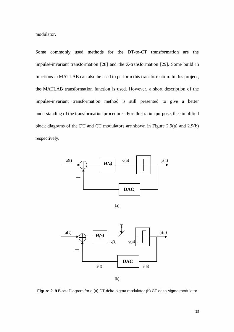
understanding of the transformation procedures. For illustration purpose, the simplified
block diagrams of the DT and CT modulators are shown in Figure 2.9(a) and 2.9(b)
respectively.
(a)
(b)
Figure 2. 9 Block Diagram for a (a) DT delta-sigma modulator (b) CT delta-sigma modulator
H(s)
DAC
u(t)
q(n)
y(n)
__
T
y(n) y(t)
q(t)
H(z)
DAC
u(t) q(n) y(n)
__
26
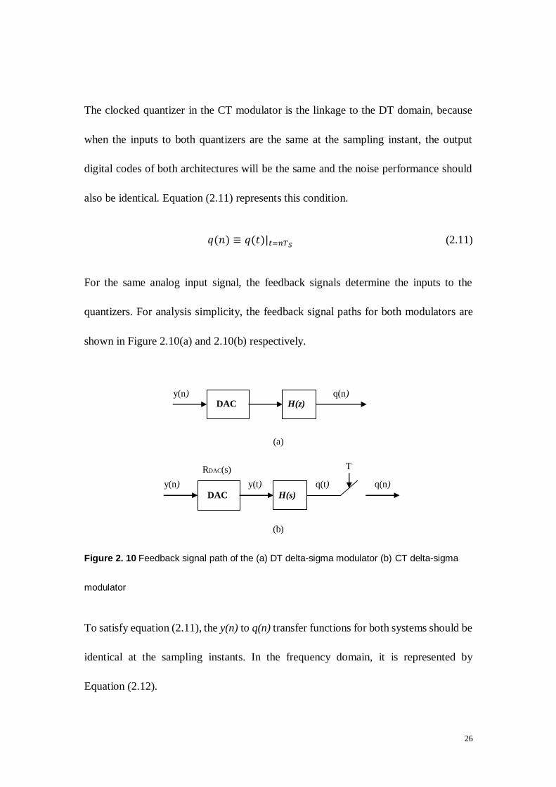
The clocked quantizer in the CT modulator is the linkage to the DT domain, because
when the inputs to both quantizers are the same at the sampling instant, the output
digital codes of both architectures will be the same and the noise performance should
also be identical. Equation (2.11) represents this condition.
(2.11)
For the same analog input signal, the feedback signals determine the inputs to the
quantizers. For analysis simplicity, the feedback signal paths for both modulators are
shown in Figure 2.10(a) and 2.10(b) respectively.
(a)
(b)
Figure 2. 10 Feedback signal path of the (a) DT delta-sigma modulator (b) CT delta-sigma
modulator
To satisfy equation (2.11), the y(n) to q(n) transfer functions for both systems should be
identical at the sampling instants. In the frequency domain, it is represented by
Equation (2.12).
DAC H(s)
y(n) q(t) y(t) q(n)
RDAC(s) T
DAC H(z) y(n) q(n)

27
(2.12)
In the time domain, Equation (2.12) leads to:
(2.13)
where represents the feedback waveform in the time domain and is the
frequency domain representation.
In the above procedures, the open-loop impulse responses for both modulators are
made equal at the sampling times, so this method is called the impulse-invariant
transformation [30]. With the use of this method, the CT loop filter can be designed to
exactly match the noise-shaping behavior of the DT loop filter. Therefore, the
performances of both modulators are identical and the transformation is successful.
2.3.4 Review of Prior Works
A summary of recently reported (year 2006-2009) low-pass CT delta-sigma modulators
is shown in Table 2.1 on the next page. Most of them are published in IEEE journal
papers. From year 2006 to 2009, there are amounts of papers published about
continuous-time delta-sigma modulators. In this work, only CT modulators with input
signal bandwidth of at least 10MHz are summarized.
The modulator performance is usually quantified by a figure of merit (FOM) as defined
by Equation (2.14).
(2.14)

28
where P is the total power consumption of the modulator and fB is the input signal
bandwidth. ENOB stands for the effective number of bits and is used to represent the
modulator resolution. It is given by Equation (2.15).
(2.15)
where DR is the dynamic range of the modulator. FOM represents the total amount of
energy required for a successful analog-to-digital conversion with specified signal
bandwidth and accuracy. The smaller the FOM is, the better the modulator overall
performance.
Table 2. 1 Summary of CT delta-sigma modulator performance from year 2006 to year 2009
Reference FOM
(pJ/conversion)
Loop Filter
Implementation Technology Order Architecture
Quantizer
(bit)
fB
(Hz)
fS
(Hz)
DR
(dB)
Supply
(V)
Power
(mW)
[7] 0.273 GmC
0.18um
1p6M
CMOS
5 CIFF 4 10M 640M 87 1.8 100
[31] 0.319 RC 65nm
CMOS 3 CIFF 3 20M 250M 60 1.2 10.5
[32] 0.55
Integrator1 and 3: SC
filter
Integrator2 :GmC
0.13um
CMOS 3 CIFB 1 10M 640M 54 1.2 5.5
[33] 0.63 RC 90nm
CMOS 2 CIFB 3 62.5M 1G 45 1 10.8
[34] 0.12 RC 0.13um
CMOS 2 CIFB 5 10M 950M 86 1.2 40
[35] 0.069 Integrator 1: RC
Integrator 2-5: GmC
90nm
CMOS 5 CIFF 4 25M 800M 75 1 16.4
[36] 0.87/1.11 RC 0.18um
CMOS 5
Modified
CIFF 4
20M/
25M 400M
60/5
5 1.8 18
[37] 0.115 GmC 0.18um
CMOS 3 CIFB 1 10M 640M 72 1.8 7.5
[38] 0.122 RC 0.13um
CMOS 3 CIFB 4 20M 640M 80 1.2 20
[39] 0.164 GmC 0.18um
CMOS 3 CIFB 1 10M 640M 67 1.8 6
[40] 6.18/5.6 RC 0.18um
CMOS 3 CIFB 4
10M
20M
100M
200M
60/5
5 1.8
101
103
As shown in the table, the input signal bandwidths of all the listed CT modulators are at

29
least 10MHz and the sampling rates are hundreds of mega hertz. The modulator orders
are generally higher than two to provide sufficient dynamic range. But the orders are
also kept below five for loop stability concerns.
In the listed publications, the modulators are implemented with either
Cascade-of-Integrator Feed-forward (CIFF) architecture or Cascade-of-Integrator
Feedback (CIFB) architecture. Both architectures belong to the single-stage topology.
Most of the referenced modulators use the CIFB structure, such as [32-34] and [37-40].
The signal-transfer-function (STF) of the CIFB modulator possess low-pass
characteristic, so any high-frequency interferences or noises to the input signal will be
filtered out. However, the signal swing at the CIFB modulator first stage output is
usually large. Therefore, this architecture is not suitable for deep sub-micron processes,
such as the 65nm CMOS process. While for CIFF modulators, the output swing at the
first stage output is much smaller. Hence, this topology is more suitable for sub-micron
technologies [31]. The drawback of this topology is the out-of-band peak in its STF.
This peak may reduce the dynamic range of the modulator in wireless applications. In
the reference paper [36], a modified CIFF architecture is used. This modulator targets
on the wireless applications, so the out-of-band peak is a very serious threat to its
performance. The modified architecture uses an extra feed-in branch to remove the
peak, which is firstly mentioned in [41]. The modulators mentioned in [7], [31] and [35]
are not specially designed for wireless applications, so normal CIFF topology is used.
More detailed discussions on the CIFF and CIFB architectures are given in Section
3.1.2.1.

30
As observed form the Table 2.1, multi-bit internal quantizers are frequently used to
increase the SNR and maintain the loop stability. Especially for the modulator with
order of five, a 4-bit internal quantizer is usually necessary to ensure the loop filter
stability [7] [35-36]. The multi-bit quantizer also reduces the clock jitter effect if the
non-return-to-zero (NRZ) feedback DAC pulse is used, as stated in [35] and [40].
However, the power consumption of the modulator using the multi-bit internal
quantizer is generally higher than that using the single-bit quantizer. The modulators
mentioned in [32] and [38] are both implemented with 0.13um CMOS process.
Comparing the two modulators, the power consumption of the multi-bit one is around
four times higher than that of the single-bit one. But the dynamic range of the single-bit
one is much smaller than that of the multi-bit one and the FOM is more than four times
higher. Therefore, the overall performance of the modulator with the multi-bit quantizer
is better. The benefits of the multi-bit quantizer are also presented later in Section 3.2.2.
With the use of the multi-bit quantizer, the multi-bit feedback DAC is inevitable in the
modulator. The elements mismatch errors of the multi-bit DAC are directly added to
the modulator output and hence degrade the overall performance [36]. Some solutions
are proposed in the listed publications. In [33], a scrambler circuit based on the data
weighted averaging algorithm (DWA) is used to suppress the mismatch error. This
method requires additional control logic in the feedback path and increases the
feedback delay. The modulator stability will be affected if the introduced delay is too
large. In [34], the DAC is directly connected to the Voltage Controlled Oscillator (VCO)
based quantizer, which provides intrinsic dynamic element matching (DEM). However,

31
the VCO based quantizer increases the design complexity and consumes lots of power.
Some of the designs adjust the transistor sizes to meet the required DAC linearity,
which is simple and straightforward as stated in [35] and [39]. The comparisons of the
possible solutions are shown in detail later in Section 3.2.3.
2.4 Summary of Chapter 2
In this chapter, some background knowledge about the delta-sigma modulator is
introduced.
The general working principles of the delta-sigma modulator are reviewed. By using
the oversampling technique, the modulator relaxes the requirements on the anti-aliasing
filter and reduces the in-band quantization noise. The delta-sigma modulator also
shapes the in-band quantization noise and increases the SNR even more.
Several optional design architectures are also discussed. For the delta-sigma modulator,
the higher order is, the larger the peak SNR. However, the loop filter stability concern
always limits the order of the modulator. The multi-stage noise shaping (MASH)
modulator solves this problem. This architecture achieves high resolution by cascading
several low-order modulators. But it is not suitable for continuous-time modulators due
to the circuit matching issues. The multi-bit delta-sigma modulator increases the SNR
by using multi-bit internal quantizer. In this architecture, the multi-bit feedback DAC
introduces some mismatch errors. Luckily, some solutions have already been proposed
[9-12].

32
In recent year, the growing need for high speed ADCs makes the CT delta-sigma
modulator more popular than its DT counterpart. A general introduction of the CT
delta-sigma modulator is presented and the comparison to the DT modulator is also
discussed. Generally, the CT delta-sigma modulator is easier to implement and operates
faster. The elimination of the anti-aliasing filter and the reduced power consumption
makes the CT modulator more suitable for high speed wideband communication
applications. The CT modulator design normally starts with the DT system synthesis.
Then the DT modulator is converted to the equivalent CT modulator. A commonly used
transformation method, the impulse invariant transformation [30], is also illustrated to
give a better understanding of the transformation procedures.
Finally, some prior works on CT delta-sigma modulators are reviewed. The design
features of the referenced modulators are presented in Table 2.1. The advantages and
drawbacks of various modulator architectures are also briefly discussed. More
systematic discussions on the architectures and building blocks are shown in detail in
the next chapter.

33
Chapter 3
System Level Design
This chapter focuses on the system level design of the modulator. Various nonideal
effects of the building blocks are described and some solutions are also proposed. The
well-developed MATLAB delta-sigma design toolbox written by Richard Schreier [42]
is used for the system level synthesis. The finalized system level model of the
modulator is determined and the modulator performance is evaluated. The system level
design results are used as references for the subsequent circuit level design.
3.1 Modulator Topology
3.1.1 System Level Parameters
For CT modulators, the single-stage topology is generally preferred to the multi-stage
one, because the matching between the analog loop and the digital cancellation logic is
difficult to achieve due to the large loop filter coefficient variations. Therefore, the
single-stage topology is selected for this design. The first step of the delta-sigma
modulator design is to determine some important system level parameters. The
decisions are made based on the performance specifications and the semiconductor
process technology to be used. In this project, 65nm CMOS process is used to

34
implement the modulator. The target signal bandwidth is 50MHz and the desired
dynamic range is around 60dB. The important system level parameters are listed below:
the oversampling ratio (OSR)
the loop filter order (L)
the number of internal quantizer bit (N)
the noise shaping or Noise Transfer Function (NTF) out-of-band gain (OOBG)
The sampling clock rate of the continuous-time delta-sigma modulator is limited by the
maximum device speed. For 65nm CMOS process, 800MHz is a quite reasonable upper
limit for the modulator sampling rate considering the gain-bandwidth requirement of
the Op Amp and the power consumption budget. Therefore, the sampling frequency is
set at 800MHz. For signal bandwidth of 50MHz, the OSR is 8. According to Equation
(2.9) in Section 2.2.1, the higher the modulator order, the higher the peak SNR. The
equation is shown below.
(2.9)
However, the modulator stability problem often limits the loop filter order. Usually, the
order should not be higher than 5 [36]. The use of multi-bit internal quantizer is an
effective way to reduce the in-band quantization noise power. Each additional quantizer
bit will improve the dynamic range (DR) by around 6dB according to Equation (2.9). In
addition, it also introduces other benefits. More aggressive noise transfer function can

35
be implemented because a multi-bit quantizer is more difficult to saturate comparing to
a single-bit comparator. The modulator loop stability is also improved due to the
significantly reduced quantization noise power. The clock jitter effect can be reduced as
well if a non-return-to-zero (NRZ) multi-bit digital-to-analog convertor (DAC) is used
in the feedback path. However, the power consumption of the quantizer also increases
proportionally to the number of quantization levels. So for a low-power design, the
quantizer bits should be optimized to get the best tradeoff between the modulator
performance and the power consumption. The target peak SNR of this project is around
60dB. At this design stage, about 20dB safety margin should be ensured. Therefore, the
SNR calculated from Equation (2.9) must be around 80dB. With the loop filter L set at
5 and oversampling ratio OSR of 8, the internal quantizer bit should be 4.
Although the last parameter NTF out-of-band gain does not appear in Equation (2.9), it
is also an important factor that affects the modulator performance a lot. Figure 3.1
shows the effect of the NTF out-of-band gain on the peak SNR. The overload input
signal levels with different NTF out-of-band gain are also plotted. Both curves are
based on MATLAB simulations. As shown in the plot, the higher the NTF out-of-band
gain is, the higher the peak SNR. However, the overload input level decreases, meaning
that the modulator becomes less stable. Based on analysis and simulations, the NTF
out-of-band gain is decided to be 3.5 to give the best tradeoff between the peak SNR
and the stability.

36
Figure 3. 1 Maximum out-of-band gain versus peak SNR and overload level
Based on extensive simulations and analysis, a fifth-order, 4-bit single-stage modulator
topology with NTF out-of-band gain of 3.5 is finally determined. The OSR is 8 and the
sampling clock rate is 800MHz.
3.1.2 Loop Filter Architecture
3.1.2.1 CIFF versus CIFB Structure
With the system level parameters determined, the second step is to determine the loop
filter architecture. For delta-sigma modulators, there are two commonly used
architectures: Cascade-of-Integrators Feedback (CIFB) and Cascade-of-Integrators
Feed-forward (CIFF). For both structures, the noise-transfer-function can be
synthesized to be the same using the delta-sigma design toolbox [42]. Therefore, the
system level performance, which is mainly measured by SNR, has no big difference.
The signal-transfer-function (STF) always affects the choice between the two structures.
One of the advantages of the CIFB structure is that its STF includes the low-pass
76.65
78.76
80.42
-0.99
-1.29-1.35
-1.6
-1.4
-1.2
-1
-0.8
-0.6
-0.4
-0.2
0
74
75
76
77
78
79
80
81
3 3.25 3.5
peak SNDR(dB)
overlod input level(dB)
NTF out-of-band gain
Peak S
NR
(d
B)
Overl
oad
in
pu
t le
vel
(dB
)

37
characteristic. What‟s more, no large adder circuit is required before the quantizer.
However, the signal swing at the output of the first stage Op Amp is usually large in the
CIFB modulator, making it difficult to implement them in the low-voltage, deep
sub-micron technology. Whereas for the CIFF architecture, the output swing of the first
stage is much smaller. Hence the first stage gain can be made large and the performance
requirements on the following stages are relaxed. Therefore, the CIFF structure is more
suitable for low-voltage applications.
However, the CIFF topology has a drawback comparing to its CIFB counterpart. There
is an unavoidable out-of-band peak in its STF. This peak equivalently reduces the
dynamic range of the modulator in wireless applications where a lot of big out-of-band
interferences exist. Figure 3.2 shows the frequency response of the STF for a fifth-order
CIFF modulator. As shown in this figure, the STF has a peak at around fS/8. If the
modulator is used in a wireless device and the interferences happen to be close to the
peaking frequency, they will be folded into the signal band due to the modulator
non-linearity. Hence the in-band noise will increase and the modulator performance
will be degraded.
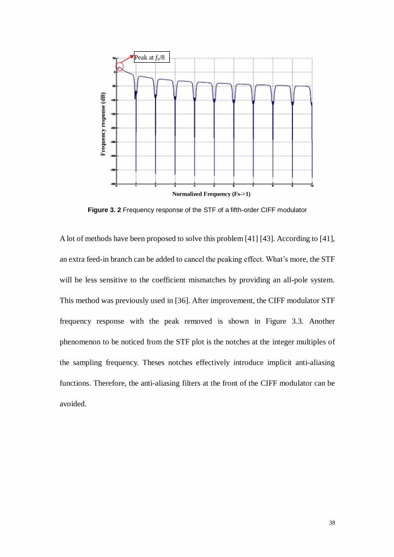
38
Figure 3. 2 Frequency response of the STF of a fifth-order CIFF modulator
A lot of methods have been proposed to solve this problem [41] [43]. According to [41],
an extra feed-in branch can be added to cancel the peaking effect. What‟s more, the STF
will be less sensitive to the coefficient mismatches by providing an all-pole system.
This method was previously used in [36]. After improvement, the CIFF modulator STF
frequency response with the peak removed is shown in Figure 3.3. Another
phenomenon to be noticed from the STF plot is the notches at the integer multiples of
the sampling frequency. Theses notches effectively introduce implicit anti-aliasing
functions. Therefore, the anti-aliasing filters at the front of the CIFF modulator can be
avoided.
Peak at fS/8
Normalized Frequency (Fs->1)
Fre
qu
ency
res
pon
se (
dB
)

39
Figure 3. 3 Frequency response of the STF of a fifth-order CIFF modulator with peak removed
3.1.2.2 Excess Loop Delay Impact
In continuous-time delta-sigma modulators, the quantizers are usually composed of
latched comparators. The quantizer outputs drive the differential input nodes of the
feedback DACs. Ideally, the DAC current should respond immediately to the quantizer
clock edge. However, in practice, the transistors in the latch and the DAC have nonzero
switching time. Thus, there exists a delay between the quantizer clock and the DAC
current pulse, which is referred to as the excess loop delay (ELD). The excess loop
delay usually consists of the delays introduced by the quantizer, the DAC and the loop
filter. The delay caused by loop filter is due to the Op Amp nonidealities, which will be
discussed in Section 3.2.1.2. For multi-bit feedback DACs, dynamic element matching
(DEM) or digital calibration circuitry are usually adapted to suppress the element
mismatch errors. These extra signal processing logics will add more delays.
Fre
qu
ency
res
pon
se (
dB
)
Normalized Frequency (Fs->1)
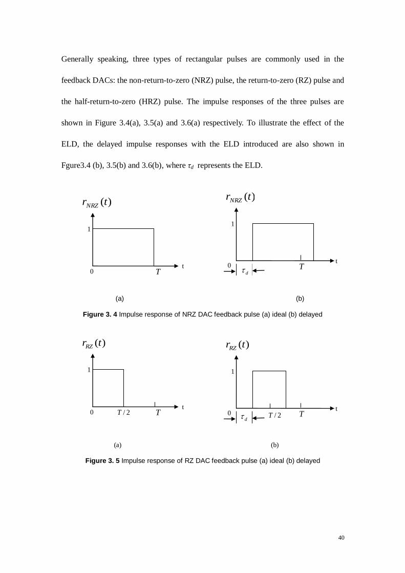
40
Generally speaking, three types of rectangular pulses are commonly used in the
feedback DACs: the non-return-to-zero (NRZ) pulse, the return-to-zero (RZ) pulse and
the half-return-to-zero (HRZ) pulse. The impulse responses of the three pulses are
shown in Figure 3.4(a), 3.5(a) and 3.6(a) respectively. To illustrate the effect of the
ELD, the delayed impulse responses with the ELD introduced are also shown in
Fgure3.4 (b), 3.5(b) and 3.6(b), where τd represents the ELD.
(a) (b)
Figure 3. 4 Impulse response of NRZ DAC feedback pulse (a) ideal (b) delayed
(a) (b)
Figure 3. 5 Impulse response of RZ DAC feedback pulse (a) ideal (b) delayed
T d
d 0
1
)(trRZ
t 2/T T 2/T 0
1
)(trRZ
t
T d
d 0
1
)(trNRZ
t
T 0
1
)(trNRZ
t

41
(a) (b)
Figure 3. 6 Impulse response of HRZ DAC feedback pulse (a) ideal (b) delayed
As shown in Figure 3.6(b), if the HRZ DAC pulse is used, part of the excess loop delay
can be absorbed by the explicit half clock delay of the pulse. As stated in [44], if the
falling edge of the DAC pulse is pushed out of one period T by the ELD, the effective
order of the CT modulator will be higher by one than that of under the ideal condition.
Hence the modulator will become unstable and the performance will be distorted.
Observing from the figures above, when HRZ DAC pulses are used, there is no such
problem as long as the delay is within half of the period. While for both NRZ and RZ
DAC pulses, even a little delay will push them out of one period T. So considering the
excess loop delay problem only, HRZ DAC is the best choice [45-46]. However, the
HRZ DAC is more sensitive to clock jitter than the NRZ DAC, as will be discussed
later in Section 3.2.2 and it‟s hard to control the excess loop delay to be within half
period. Therefore, NRZ DAC is used as the feedback signal in this project. More
detailed discussions about the choice of the feedback DAC pulse will be given in
Section 3.2.2.
Using the NRZ DAC, the tolerable excess loop delay is only about 16% of the sampling
T
d
d
0
1
)(trHRZ
t 2/T T 2/T 0
1
)(trHRZ
t

42
period TS, as shown by the simulation results in Figure 3.7. This figure shows the plot of
the peak SNR versus varying excess loop delays. The input level where the peak SNR
occurs is also displayed. When the delay is 16% of TS, the SNR decreases less than 3dB.
After passing though the point 0.16Ts, the peak SNR drops suddenly and the dynamic
range shrinks a lot. The power spectra density (PSD) plots for the modulator output
with excess loop delay of 0, 0.16Ts and 0.2Ts are shown in Figure 3.8 for comparison.
As can be observed from the figure, when the excess loop delay is 0.2Ts, the modulator
becomes unstable and the loop filter response is out of control.
Figure 3. 7 Peak SNR and input level plots versus excess loop delay
-9
-8
-7
-6
-5
-4
-3
-2
-1
0
0
10
20
30
40
50
60
70
80
90
0.02 0.04 0.06 0.08 0.1 0.12 0.14 0.16 0.18
Psndr(dB)
input level(dB)
Excess loop delay (Ts)
Peak S
NR
(d
B)
Inp
ut
level (d
B)

43
Figure 3. 8 PSD plots for the modulator output with ELD of 0, 0.16Ts and 0.2Ts
As proposed in [7] and [47], to solve the excess loop delay problem, an explicit
one-period delay is inserted at the quantizer output to absorb the varying excess loop
delay. A second feedback path is also added to the input of the quantizer to make the
impulse response of the CT modulator equivalent to its DT counterpart. The block
diagram of the modulator is shown in Figure 3.9. The additional feed-in branch b1 is
used to flatten the STF peak, as mentioned before in Section 3.1.2.1.
Normalized Frequency (Fs->1)
PS
D (
dB
)

44
Figure 3. 9 CT modulator with additional feedback path to alleviate excess loop delay effect
3.1.3 Loop Filter Coefficient Assignment
With the loop filter topology confirmed, the next step is to determine the block
coefficients. Using the delta-sigma design toolbox, the noise-transfer-function of the
modulator‟s DT counterpart is determined as shown below.
(3.1)
The zeros of NTF transfer function are optimized to suppress the in-band quantization
noise. The locations of the zeros and poles are shown in Figure 3.10.
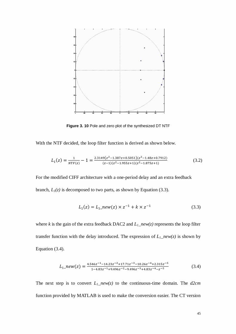
45
Figure 3. 10 Pole and zero plot of the synthesized DT NTF
With the NTF decided, the loop filter function is derived as shown below.
(3.2)
For the modified CIFF architecture with a one-period delay and an extra feedback
branch, L1(z) is decomposed to two parts, as shown by Equation (3.3).
(3.3)
where k is the gain of the extra feedback DAC2 and L1_new(z) represents the loop filter
transfer function with the delay introduced. The expression of L1_new(z) is shown by
Equation (3.4).
(3.4)
The next step is to convert L1_new(z) to the continuous-time domain. The d2cm
function provided by MATLAB is used to make the conversion easier. The CT version

46
of L1_new (z) is shown by Equation (3.5) below.
(3.5)
The CT loop filter transfer function can also be derived from the system level
architecture based on the block coefficients. The additional input branch is not taken
into consideration firstly. The numerator and denominator part of the transfer function
are extracted from MATLAB simulations as shown by Equation (3.6) and (3.7)
respectively.
(3.7)
By matching the numerator and denominator of Equation (3.5) with Equation (3.6) and
(3.7) respectively, the block coefficients before dynamic scaling are determined as
shown in Table 3.1. The MATLAB simulation codes are attached in Appendix A.

47
Table 3. 1 Block Coefficients before Dynamic Scaling
k1 3.2785 g1 1 gz1 1 C2 1
k2 2 g2 0.3052 gz2 0.1
k3 0.0633 g3 2.13 k 2.3149
k4 1 g4 0.9312 b1 -5.5
k5 0.4471 g5 0.1695 c1 1
As explained in previous sections, the additional feed-in branch b1 is added to remove
the peak in the modulator signal-transfer-function. The new loop filter transfer function
L0(s) with the additional input branch is shown by Equation 3.8. Figure 3.11 plots the
frequency responses of L0(s), STF(s) and NTF (z).
(3.8)
Figure 3. 11 Frequency responses of transfer functions
The SNR is plotted versus the input level in Figure 3.12. The peak SNR is 80.63dB and
occurs at -2dB of full scale input level, VFS. The PSD plot for peak point has already
STF
NTF
L0
Normalized Frequency (Fs->1)
Gain
(d
B)
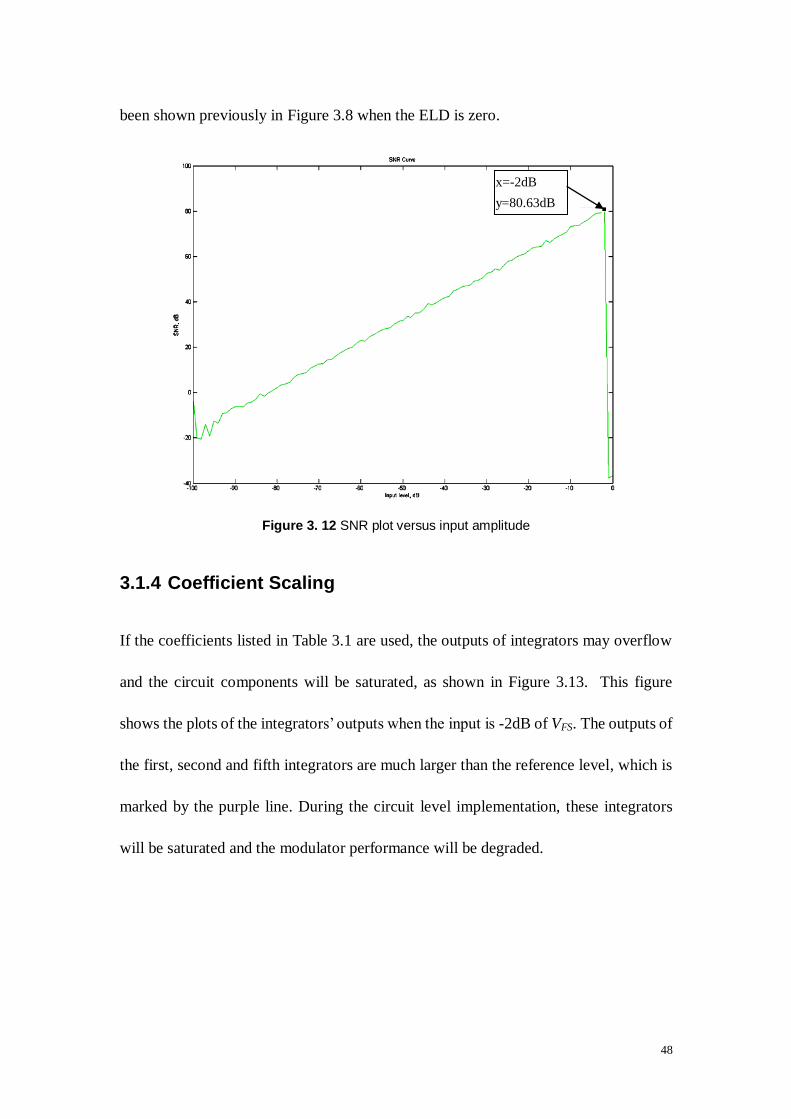
48
been shown previously in Figure 3.8 when the ELD is zero.
Figure 3. 12 SNR plot versus input amplitude
3.1.4 Coefficient Scaling
If the coefficients listed in Table 3.1 are used, the outputs of integrators may overflow
and the circuit components will be saturated, as shown in Figure 3.13. This figure
shows the plots of the integrators‟ outputs when the input is -2dB of VFS. The outputs of
the first, second and fifth integrators are much larger than the reference level, which is
marked by the purple line. During the circuit level implementation, these integrators
will be saturated and the modulator performance will be degraded.
x=-2dB
y=80.63dB

49
Figure 3. 13 Integrator outputs of un-scaled integrators
Generally the integrator output is desired to be 20% less than the reference voltage at
-2dB of full scale input to ensure system stability [48]. In this design, more safety
margin is given to ensure the proper performance of the modulator. The maximum
values of the integrators‟ outputs should not exceed 40% of the reference voltage.
Besides, the optimization of power consumption also needs to be taken into account
when scaling the coefficients. Because the larger the integrator coefficient is, the larger
its gain-bandwidth product (GBW). The current consumption of the integrator will be
higher as well. The detailed discussion of how the integrator coefficient is related to its
power consumption will be presented later in the circuit level design.
In general, the internal states may not reach their maximum values when a single-tone
sinusoidal signal is placed at the input. In practice, other signals may present at the

50
same time. According to [48], to make the internal states reach their maximum values
before the modulator becomes unstable, a slowly raised DC input with certain level of
random noise can be employed. The random noise is set to have mean zero with
standard deviation of 5% of the DC amplitude. As depicted in Figure 3.14, the dynamic
scaling is performed by reducing the incoming branches by a factor k and increasing the
outgoing branches by the same factor k to compensate the attenuation [49]. In this
manner, only the integrators‟ outputs are altered without affecting the loop filter
characteristic. The coefficients after scaling are shown in Table 3.2 and the maximum
values of the internal states against different input magnitudes are plotted in Figure
3.15.
(a)
(b)
Figure 3. 14 (a) Blocks before coefficient scaling (b) blocks after coefficient scaling
b
c
f(z) or f(s)
a d
e
f
x
f(z) or f(s)
a/k
b/k
c/k
d*k
e*k
f*k
x/k

51
Figure 3. 15 Internal states maximum values plot after scaling
Table 3. 2 Block Coefficients after Dynamic Scaling
k1 0.2786 g1 11.7648 gz1 9.1 c2 12.195
k2 0.164 g2 3.7218 gz2 0.8876
k3 0.007 g3 19.383 k 2.3149
k4 0.6667 g4 9.0792 b1 -5.5
k5 0.075 g5 9.7812 c1 11.7648
With the new coefficients, the integrator outputs are all bounded within 40% of the
reference level, as proven by Figure 3.16. Figure 3.17 presents the SNR versus the input
plots before and after the coefficient scaling. The two curves overlap, meaning that the
loop filter characteristic is not affected after the coefficient scaling.
0
20
40
60
80
100
120
140
0 -1 -2 -3 -4 -5 -10 -15 -20 -25 -30 -35 -40 -50 -60 -70
max. value of 1st integrator output
max. value of 2nd integrator output
max. value of 3rd integrator output
max. value of 4th integrator output
max. value of 5th integrator output
Internal States Maximum Values in CT Modulator after Dynamic Scaling
Input Level (dBFS)
Max.
Inte
gra
tor
Ou
tpu
t R
ela
tiv
e t
o F
S (
%)

52
Figure 3. 16 Integrator outputs of scaled integrators
Figure 3. 17 SNR versus input level plot comparisons between both sets of coefficients
3.2 Nonidealities in Continuous-Time Delta-Sigma Modulators
After the CT loop filter topology and block coefficients determined, the modulator must
-60
-40
-20
0
20
40
60
80
100
0 -4 -8
-12
-16
-20
-24
-28
-32
-36
-40
-44
-48
-52
-56
-60
-64
-68
-72
-76
-80
-84
-88
-92
-96
-10
0
SNR(dB) with unscaledcoefficients
SNR(dB) with scaledcoefficients
SN
R (
dB
)
Input Level (dBFS)

53
be implemented using real circuit blocks. Different from the components used in
Section 3.1, real circuits have many inherent nonideal effects, which may degrade the
modulator performance and even cause system instability. In this section, various
nonidealities are discussed, including the integrator nonidealities, the clock jitter noise
and the multi-bit DAC element mismatch error. Each issue is investigated and proper
models are built to examine their influences on the modulator performance. Some
possible methods to reduce the impacts are also discussed.
3.2.1 Integrator Nonidealities
As one of the most important building blocks of a delta-sigma modulator, the integrator
design affects the loop filter response significantly. Therefore, the selection of the
integrators must be carried out carefully. As well known, there are three commonly
used types of integrators, GmC-integrators, RC-integrators and LC-resonators.
Generally, LC-resonators are mostly used as loop filters in band-pass delta-sigma
modulators [50]. Therefore, it‟s not used in the low-pass modulator design. The
simplified schematic of GmC and RC integrators are shown in Figure 3.18 (a) and (b)
respectively.
(a) (b)
Figure 3. 18 Simplified schematic for fully differential (a) RC-integrator (b) GmC-integrator
54
Assuming that the operational amplifier (Op Amp) is ideal for the RC-integrator and
the transconductor is ideal for the GmC-integrator, the output transfer functions of the
two blocks are derived as shown by Equation (3.9) and (3.10) respectively.
(3.9)
(3.10)
Generally speaking, RC-integrators have higher linearity and larger input signal swing
comparing to their GmC counterparts [28]. Due to the closed-loop structure of the
RC-integrator, the Op Amp‟s inputs are virtual ground and experience very small signal
swings regardless how large the integrator‟s input signals are. While for
GmC-integrators, open-loop structures are used. The transconductor‟s inputs have to
experience the full swing of the integrator‟s input signals, so the linearity of the
integrators is degraded.
The first stage of the loop filter is the most critical part in the modulator, because any
noise or distortions from this stage will be added directly to the modulator output
without any attenuation. Therefore, to ensure the modulator performance, both the first
integrator and the first feedback DAC have to be very linear. As a result, the first
integrator in the loop filter is implemented with RC-integrator for its superior linearity.
Another benefit provided by using RC-integrator is the improvement of the feedback
DAC linearity. Because the DAC output is connected to the Op Amp‟s virtual ground
input nodes, it will not experience large signal variations. If a GmC-integrator is used,
the DAC‟s output has to be connected to the output of the integrator and sustain full

55
signal swing. The DAC linearity will degrade a lot.
On the other hand, due to the open-loop working condition, the GmC-integrators are
generally faster than the RC-integrators [27]. Therefore, for a given bandwidth
requirement, the power consumption of the GmC-integrator is lower. As a result, the
second to fifth integrators are implemented using the GmC structure. For both types of
integrators, there are some nonidealities that must be taken into consideration during
the design process. In the following subsections, these nonidealities are discussed in
detail.
3.2.1.1 Finite Integrator DC Gain
Under ideal conditions, it is common to assume that the Op Amps have infinite gain and
the transconductors have infinite output resistance. The transfer functions of an ideal
RC-integrator and an ideal GmC-integrator are shown by Equation (3.9) and (3.10)
respectively. However, in deep sub-micron applications, the Op Amp‟s DC gain can
seldom be boosted up to 60dB and the transconductors usually have finite output
impedances. The simplified single-end models for both integrators are shown in Figure
3.19 (a) and (b) respectively, where Ao stands for the finite Op Amp DC gain and Rout
represents the limited transconductor output resistance.

56
(a) (b)
Figure 3. 19 Single-end models for (a) RC-integrator with finite DC gain (b) GmC-integrator
with finite output resistance
Using the above models, the transfer functions for the integrators are derived as shown
by Equation (3.11) and (3.12) respectively.
For RC-integrator:
(3.11)
For GmC-integrator:
(3.12)
where stands for the DC gain of the transconductor. The effect from the
finite transconductor output resistance is often referred to as leaky integration [28]. The
noise floor will be raised by this nonideality.
To find out the effect of the integrator finite gain on the modulator performance, the
signal to noise and distortion ratio (SNDR) is plotted versus the integrator DC gain. The
input signal is set at -2dB of full scale voltage level. The plots are shown in Figure
3.20(a) and (b).

57
(a)
(b)
Figure 3. 20 SNDR plot versus DC gain of (a) first and second integrator (b) third to fifth
integrator
As observed from the plots, the SNDR drops with the integrators‟ gains. To constrain
the drop of the SNDR within 3dB, the minimum gain requirements on integrators are
summarized in Table 3.3. The gain requirement of the first integrator is the highest,
because any nonidealities from this stage will affect the modulator SNDR directly. For
the following stages, the requirements are relaxed subsequently. In the circuit design,
0
10
20
30
40
50
60
70
80
90
20 22 24 26 28 30 32 34 36 38 40 42 44 46 48 50 52 54 56 58 60
1st integrator DC gain(dB)
2nd integrator DC gain(dB)
-40
-20
0
20
40
60
80
100
0 1 2 3 4 5 6 7 8 9 10 11 12 13 14 15 16 17 18 19 20
3rd integrator DC gain(dB)
4th integrator DC gain(dB)
5th integrator DC gain(dB)
Integrator DC Gain (dB)
SN
DR
[d
B]
SN
DR
[d
B]
Integrator DC Gain (dB)

58
Table 3.3 will be used as a reference to design the integrators.
Table 3. 3 Minimum DC gain requirements of integrators
First Integrator minimum DC gain 40dB
Second Integrator minimum DC gain 30dB
Third Integrator minimum DC gain 15dB
Forth Integrator minimum DC gain 15dB
Fifth Integrator minimum DC gain 10dB
3.2.1.2 Finite Gain Bandwidth Product (GBW) of Op Amp
An ideal Op Amp is always treated as a voltage-controlled voltage source with an
infinitely large gain across the whole frequency domain. While in reality, an Op Amp
has a finite DC gain and several poles and zeros in its transfer function. To make the
analysis simple, it‟s common and reasonable to approximate the real Op Amp‟s transfer
function by a single-pole system, as shown by Equation (3.13).
(3.13)
where Ao stands for the DC gain and is the pole frequency. For a general n-input RC
integrator shown in Figure 3.21, the transfer function from the ith
input to the output is
derived with the single-pole model, as shown by Equation (3.14) [36].
(3.14)
Since Ao is always much larger than 1 in real case, Equation (3.14) can be simplified as
shown by Equation (3.15).

59
(3.15)
where is the gain bandwidth product of the Op Amp.
Figure 3. 21 An n-input RC integrator
The RC time constant is usually normalized to the sampling frequency fS of the CT
modulator, as show below.
(3.16)
where is the integrator block coefficient.
Comparing Equation (3.15) with the ideal transfer function shown by Equation (3.9),
two additional terms are introduced by the finite GBW, the gain error (GE) and a second
pole ( ). The expressions for the two items are derived as shown below.
(3.17)
(3.18)
Therefore, Equation (3.15) can be simplified as below.

60
(3.19)
With finite GBW, the first integrator of the modulator can be represented using the
model derived above. It is shown in Figure 3.22, where Ku and Kb1 are the input feed-in
and DAC feedback coefficients respectively. In this design, Ku and Kb1 have the same
value.
Figure 3. 22 First stage of the CT delta-sigma modulator with the nonideal model for RC
integrator
The effect of the gain error can be simply compensated by adjusting the block
coefficients. The second pole effectively adds a low-pass filter in both the feed-in
and feedback paths, as depicted by the model in Figure 3.23. Since is normally much
higher than the input signal frequency, the additional pole has little effect on the feed-in
path. Whereas for the feedback branch, the low-pass filter effectively adds in a delay,
which affects the modulator performance in the same way as the excess loop delay.
Ku
DAC
Kb1
-
u

61
Kb1
-
u
Ku
Figure 3. 23 Equivalent model for the first stage of the CT delta-sigma modulator
To find out the acceptable GBW range of the first integrator Op Amp, the model shown
in Figure 3.22 is used for the RC-integrator in MATLAB simulations. The SNDR
versus Op Amp GBW plot with -2dB of full scale input is shown in Figure 3.24. As
observed from the plot, to ensure the SNDR drops within 3dB, the GBW of the first
integrator Op Amp has to be around 3fS. In this project, the sampling frequency fS is set
at 800MHz. Therefore, during the circuit implementation, the Op Amp should have a
GBW of around 2.4GHz.
Figure 3. 24 SNDR versus GBW plot with input at -2dB of full scale
-60
-40
-20
0
20
40
60
80
100
1 1.2 1.4 1.6 1.8 2 2.2 2.4 2.6 2.8 3 3.2 3.4 3.6 3.8 4 4.2 4.4 4.6 4.8 5
SNR (dB) @ input =-3dB Full Scale
DAC
RC-Integrator Op Amp GBW (fs)
SN
DR
[d
B]

62
3.2.2 Clock Jitter Effect
In continuous-time delta-sigma modulators, both the quantizer and feedback DACs are
controlled by clock signals. For CT modulators, the sampling process takes place at the
input of the quantizer. Therefore, similar to the quantization noise, the sampling error
caused by the clock jitter is shaped by the loop filter. As a result, this error induced by
the clock jitter is suppressed and may be neglected. However, the DAC feedback signal
error due to the clock jitter is very important, especially in CT delta-sigma modulators
[51]. Since the DAC output of the CT modulator is continuous, the feedback signal
affects the loop filter all the time instead of just at the sampling instants. What‟s more,
the timing error of the DAC feedback signal appears at the modulator output without
any attenuation. As a result, the modulator performance will be degraded. Therefore,
the DAC clock jitter is one of the most important design issues for the CT modulators.
The choice of the feedback DAC pulse shape plays an important role on the effect of the
clock jitter error. Figure 3.25 shows the single-bit NRZ, RZ and HRZ pulses with clock
jitter error injected. The solid lines indicate that the clock edges are affected by jitter. As
can be observed from the figure, the NRZ DACs are affected by the jitter only when the
output changes. While for the RZ and HRZ DACs, both rising and falling edges of
pulses occur in each clock cycle, so they are affected by clock jitter more frequently.

63
Figure 3. 25 Single-bit NRZ, RZ and HRZ DAC pulses with clock jitter effect
If multi-bit NRZ feedback DAC pulses are used, the jitter noise power will be lower,
because the standard deviation of the adjacent modulator output difference is reduced.
The multi-bit feedback DAC pulses are shown in Figure 3.26. By intuition, the
multi-bit NRZ DAC pulse provides better clock jitter immunity than the other two types,
because its output does not need to return back to zero for every clock cycle and hence
the average adjacent output difference is smaller. The following equations prove this
statement.
Figure 3. 26 Multi-bit NRZ, RZ and HRZ DAC pulses with clock jitter effect
1 -1 1 -1 -1
NRZ
RZ
HRZ
NRZ
RZ
HRZ

64
The error sequence expression for the NRZ DAC is derived and shown by Equation
(3.20) below.
(3.20)
where y(n) is the nth
output bit, Δt is the clock edge timing error and TS is the sampling
clock period.
Assuming that the wideband clock jitters are uncorrelated, the energy of the jitter error
for the NRZ pulse is derived as below.
(3.21)
where is the standard deviation of the adjacent output difference, and is the
standard deviation of the clock jitter. Similarly, the jitter error energy equation for the
RZ and HRZ DAC pulses are shown by Equation (3.22) and (3.23) respectively.
(3.22)
(3.23)
Different from the NRZ DAC, the jitter energy of the RZ and HRZ pulses are
proportional to the output values other than the output differences. Since the pulses are
affected twice in one clock cycle, there are coefficients „2‟ in the above two equations.
The three pulses with clock jitter are compared and the ratios of the jitter error energy
equations are derived, as shown by the following two equations.

65
(3.24)
(3.25)
If the three types of multi-bit DAC pulses have the same full scale output level, both
Equation (3.24) and (3.25) will be smaller than one, meaning that the NRZ pulse is less
sensitive to clock jitter than the other two types do. A good rule of thumb is that CT
modulators employing RZ or HRZ DACs experience jitter noise about 6dB worse than
if NRZ DACs are used [51]. Therefore, the NRZ DAC is chosen as the feedback pulse.
To simulate the effect of clock jitter, a random error is added to the feedback signal to
model the error caused by the DAC clock jitter. After that, a series of simulations are
performed and the results are shown in Figure 3.27. The SNDR is plotted against the
clock jitter at -2dB of full scale input. The higher the clock jitter is, the lower the peak
SNDR. If 3dB degradation of SNDR is allowable, the clock jitter should not be higher
than 0.09%TS, which is 1.125ps.
According to [36], some of the off-chip circuit, such as the clock generators based on
LC voltage-controlled oscillators (VCOs), can achieve sub-picoseconds jitter
performance. In this project, these external clock sources can be used to generate the
clock control signals. Therefore, the clock jitter can be controlled to be lower than
0.09%TS and an ideal clock generator is used in the circuit level design.

66
Figure 3. 27 SNDR versus clock jitter plot at -2dB full scale input
3.2.3 DAC Non-linearity
As stated in previous sections, the use of multi-bit quantizer provides several benefits:
the SNR is increased, the modulator stability is improved and the clock jitter effect is
reduced. However, there are also some side effects of using a multi-bit quantizer. For
the multi-bit system, the multi-bit feedback DAC is inevitable, for which the element
mismatch problem is unavoidable. Figure 3.28 shows the simplified block diagram of a
multi-bit modulator with the DAC element mismatch error. The mismatch error is
represented by the signal d. The output transfer function can be easily derived from this
model, as shown by Equation (3.26).
(3.26)
where MTF(z) represents the mismatch error transfer function and D(z) is the mismatch
0
10
20
30
40
50
60
70
80
90
0.0
1
0.0
5
0.0
9
0.1
3
0.1
7
0.2
1
0.2
5
0.2
9
0.3
3
0.3
7
0.4
1
0.4
5
0.4
9
0.5
3
0.5
7
0.6
1
0.6
5
0.6
9
0.7
3
0.7
7
0.8
1
0.8
5
0.8
9
0.9
3
0.9
7
4bit PSNDR @ input of -2dBFS (dB)
Clock Jitter Effect (%fs)
SN
DR
[d
B]
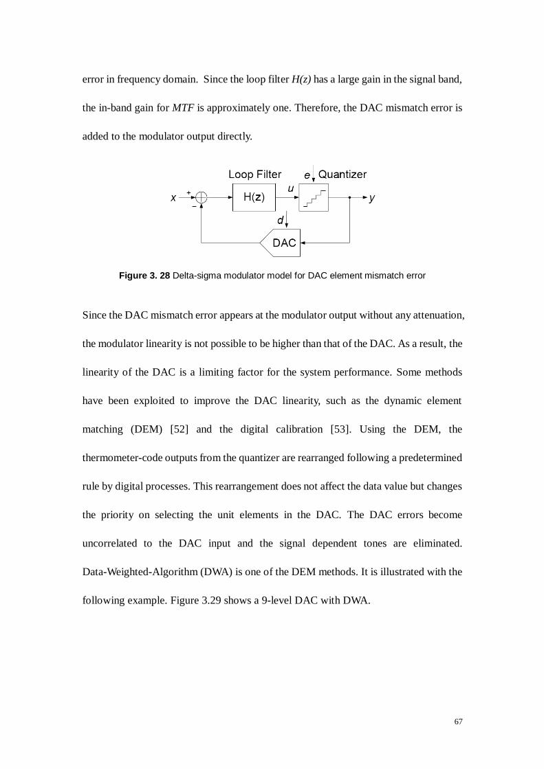
67
error in frequency domain. Since the loop filter H(z) has a large gain in the signal band,
the in-band gain for MTF is approximately one. Therefore, the DAC mismatch error is
added to the modulator output directly.
Figure 3. 28 Delta-sigma modulator model for DAC element mismatch error
Since the DAC mismatch error appears at the modulator output without any attenuation,
the modulator linearity is not possible to be higher than that of the DAC. As a result, the
linearity of the DAC is a limiting factor for the system performance. Some methods
have been exploited to improve the DAC linearity, such as the dynamic element
matching (DEM) [52] and the digital calibration [53]. Using the DEM, the
thermometer-code outputs from the quantizer are rearranged following a predetermined
rule by digital processes. This rearrangement does not affect the data value but changes
the priority on selecting the unit elements in the DAC. The DAC errors become
uncorrelated to the DAC input and the signal dependent tones are eliminated.
Data-Weighted-Algorithm (DWA) is one of the DEM methods. It is illustrated with the
following example. Figure 3.29 shows a 9-level DAC with DWA.

68
Figure 3. 29 Illustration of DWA
The grey grids represent the currently used elements and the white ones show the idle
elements. The number of elements to be used is equal to the input data value, which is
shown on the left of the element array. The elements are selected in a circular way, so
that each element has the same probability of usage. Therefore, the mismatch among
the cells can average out and the error is effectively first-order shaped.
Another commonly used technique to improve the DAC linearity is the digital
calibration. In this method, a reference current source is used as a standard to trim each
current cell circularly. Since a current cell cannot produce valid output during the
calibration phase, a spare one is needed to ensure the accuracy of the DAC output.
Therefore, for a 15-level feedback DAC, 16 current sources are required in total.
Both methods mentioned above require extra signal processing logics in the feedback
path. In real circuit implementations, these extra logics will add more excess loop delay
and the modulator will become less stable. Therefore, the above two methods are not
suitable for this project. According to some publications [35], the element matching
accuracy can also be improved by adjusting the size of the current source transistor in
1 2 3 4 5 6 7 8 9
2
4
5
7
6
3
Data
DAC Elements

69
each cell. The formula of Bosch et al.[54] and the Pelgrom model [55] are used to
calculate the proper transistor size to achieve the required DAC linearity. Since this
method is easy to implement and the modulator stability is not affected, it is used in this
project to improve the DAC linearity.
The PSD curves for the modulator with an ideal DAC and a 12-bit linearity DAC are
shown in Figure 3.30. For the modulator with the DAC linearity of 12bits, the peak
SNR is around 80dB. It is quite close to that of the ideal one and the modulator
performance does not degrade too much. Therefore, the DAC linearity of 12bits is
acceptable for this design. In the circuit level design, the DAC current source transistors
sizes should be adjusted to achieve the linearity of 12bits.
Figure 3. 30 PSD plot for DAC pulses

70
3.2.4 Summary of Nonidealities
Table 3.4 below summarizes all the nonidealities that have been mentioned above. They
are all included to test the modulator performance. The input signal is swept across the
entire dynamic range to evaluate the modulator SNR, as shown in Figure 3.31. The
system level design of the modulator achieves a dynamic range of 74dB and the ENOB
is 12bits. The peak SNDR is around 74 dB. The PSD plot for the modulator output is
also shown in Figure 3.32.
Table 3.4 Nonidealities summary
Modulator Nonidealities Value
Excess loop delay TS
First Integrator minimum DC gain 40dB
Second Integrator minimum DC gain 30dB
Third Integrator minimum DC gain 15dB
Forth Integrator minimum DC gain 15dB
Fifth Integrator minimum DC gain 10dB
First integrator Op Amp GBW 3fS
Clock jitter 0.09%TS
DAC linearity 12bits

71
Figure 3. 31 SNR versus full dynamic range
Figure 3. 32 PSD plot for modulators

72
3.3 Summary of Chapter 3
In this chapter, the system level design of the modulator is described in detail. The
MATLAB delta-sigma toolbox is used for the system level synthesis.
The four important system level parameters are determined firstly. The modulator
order is set at 5 due to the stability consideration [36]. The sampling rate is limited by
the maximum device speed. For 65nm CMOS process, 800MHz is a quite reasonable
sampling frequency and hence the oversampling ratio is 8. A 4-bit internal quantizer is
chosen for the modulator to give the best performance and power consumption tradeoff.
Finally, based on extensive simulations, the noise-transfer-function out-of-band gain is
set at 3.5.
The Cascade-of-Integrators Feed-forward topology is selected to implement the
modulator due to its low swing at the first stage output. An extra feed-in branch is added
to remove the inherit peak in its signal-transfer-function. To make the modulator more
immune to the excess loop delay, a one-period delay is inserted to absorb the delay and
an extra feedback branch is also added. The final modulator topology is shown in
Figure 3.9.
The loop filter block coefficients are determined with enormous use of the delta-sigma
toolbox. The coefficients are calculated based on the modulator topology. The
frequency responses of the modulator transfer functions are shown in Figure 3.11.
Proper scaling is also performed on the coefficients to bind the integrators‟ outputs
within the safety level. The final coefficients are shown in Table 3.2. The peak SNR of
73
the ideal modulator is around 80dB as shown in Figure 3.17.
In the circuit level implementations, there will be various nonidealities for the block
components. The effects from the nonidealities are also investigated in this chapter.
Some possible solutions are discussed as well.
The first integrator of the modulator is to be implemented with the RC-integrator
topology for its superior linearity. For the second to fifth integrators, the
GmC-integrator topology will be used due to its lower power consumption. For both
types of integrators, the DC gain cannot be infinite and hence the integrator‟s transfer
function is different from that of the ideal one. The peak SNR of the modulator
degrades consequently. The effects from the finite DC gain are shown in Figure 3.20(a)
and (b). The minimum gain requirement on each integrator is shown in Table 3.3. This
table will be used as a reference for the integrators design. For the RC-integrator, the
finite gain bandwidth product of the Op Amp effectively introduces an extra delay in
the feedback path (Fig. 3.23). Figure 3.24 shows the effect of the limited GBW on the
modulator‟s performance. The Op Amp‟s GBW must be around three times of the
sampling frequency (fS) to ensure that the SNDR drops less than 3dB. Hence, during
the circuit design, the GBW of the Op Amp should be around 2.4GHz.
The CT modulator is very sensitive to the clock jitters, especially in its feedback path.
The timing errors of the DAC feedback signals will appear at the modulator output
directly and hence degrade the modulator performance. Based on analysis, NRZ pulses
are more immune to the clock jitters comparing to RZ and HRZ pulses. Therefore, the

74
NRZ DAC is selected for the feedback path. The clock jitter effect is shown in Figure
3.27. To ensure the modulator performance, the clock jitter should be lower than 0.09%
of the sampling period (TS).
In this project, a multi-bit internal quantizer is used to improve the modulator
performance. Therefore, multi-bit DACs must also be used in the feedback paths. The
unavoidable element mismatch error in the multi-bit DAC will be added to the
modulator output directly and hence the modulator linearity is limited. Some methods,
such as dynamic element matching [52] and digital calibration [53], have been
proposed to solve this problem. However, using these methods will introduce more
delays in the feedback path, which affects the modulator stability. Therefore, they are
not adapted. In this design, the DAC linearity is to be improved by adjusting the size of
the current source transistor in each feedback element [35]. Based on simulations, the
acceptable DAC linearity is around 12bits, as proven by Figure 3.30. Therefore, the
DAC transistor sizes should be adjusted to achieve the linearity of 12bits in the circuit
design.
Finally, with all the nonidealities included (Table 3.4), the system level design of the
modulator achieves a dynamic range of 74dB with about 12dB margin reserved for the
circuit design. The effective number of bit is 12bits. With the system level synthesis of
the modulator completed, the circuit level design will be carried on in the next chapter.

75
Chapter 4
Circuit Implementation
With the system level coefficients determined and the nonideal effects checked, the
next step is to implement the blocks using real circuit components. In this chapter, the
circuit design of various blocks is discussed in detail.
4.1 Top Level Circuit
The top level circuit diagram is shown in Figure 4.1. As shown in this figure, the first
integrator is a RC-integrator and the second to fifth integrators are implemented using
GmC-integrator configuration. The integration capacitors are placed on each side of the
integrator output branch to balance the output stage. All the gain stages are realized by
transconductors to convert voltages into currents. The currents are then added together
and then converted back to voltage by the summing circuit. The quantizer takes
samples from the summing circuit outputs and then generates thermometer codes,
which are used to control the two current steering feedback DACs. As can be observed,
there is a D-latch delay between the two DACs. It is used to absorb the excess loop
delay from the quantizer. The DAC2 is added to compensate the inserted delay and its
output is directly feed into the quantizer. The output of DAC1 is connected to the
RC-integrator input nodes, which are actually virtual ground. Hence the linearity of the

76
DAC is ensured. All the circuit components mentioned above are built based on 65nm
CMOS technology.

77
Figure 4. 1 Top-level circuit block diagram

78
4.2 RC-Integrator Design
As shown in the top level circuit diagram, the first integrator is a RC-integrator due to
the stringent requirement on the linearity despite the fact that the power consumption of
the RC-integrator is generally higher than that of the GmC-integrator. Another
advantage compared to using the GmC-integrator is the virtual ground at the input
nodes, which provides stable output biasing for the current steering feedback DAC and
hence good DAC linearity can be achieved.
4.2.1 The Op Amp in the RC-Integrator
For low-voltage design, two types of Op Amp structures are usually used: the two-stage
and the folded-cascode Op Amps. Since in this project, the amplifier of the
RC-integrator does not need to drive a pure resistive load, a single-stage amplifier is
more suitable for fast operation and consumes less power [39]. Comparing to the
telescopic cascode single-stage topology, folded-cascode one is slower and the power
consumption is generally larger. However, it uses less voltage headroom and hence
provides larger output signal swing, which is highly desired for the system
implemented with nanometer technology [32]. One problem associated with the
folded-cascode amplifier implemented with 65nm CMOS process is that the DC gain
can hardly exceed 40dB, which is the minimum gain requirement for the first integrator,
as set in the MATLAB simulations. Therefore, if the designed amplifier cannot achieve
the DC gain of 40dB, a gain-boosting method will be utilized, which increases the gain
by additional gain stage without compromising the signal swing and gain bandwidth
product (GBW) of the original amplifier [35].
The selected folded-cascode topology is shown in Figure 4.2 below. This topology is

79
chosen for its low power consumption and simplicity of transistor‟s size adjustment.
Common-mode feedback (CMFB) circuit is required to generate the cmfb signal to
maintain the output common-mode voltage.
Figure 4. 2 RC-integrator Op Amp topology
The first stage of the loop filter has the most stringent noise requirement, because the
noise from this stage is directly added to the output signal without any attenuation.
Therefore, the design of the first integrator is mainly concerned with the noise
requirements other than power consumption. There are two noise sources from the
RC-integrator: the input resistor and the amplifier. The noise power spectra density
(PSD) generated by the two input resistors is shown by Equation (4.1).
(4.1)
where k is Boltzmann‟s constant with a value of and T is the absolute
temperature. R represents the input resistor. To reduce the thermal noise from the
resistors, large resistor value should not be used.
The differential input-referred thermal noise from the amplifier is given by the
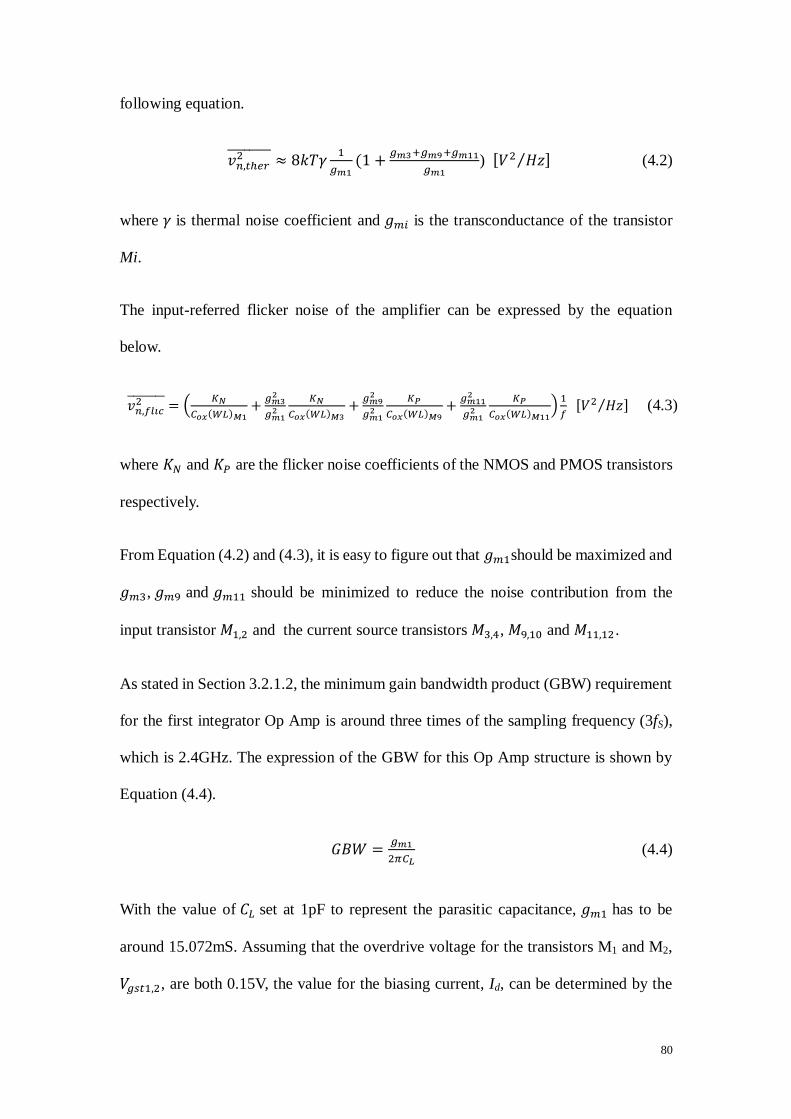
80
following equation.
) (4.2)
where is thermal noise coefficient and is the transconductance of the transistor
Mi.
The input-referred flicker noise of the amplifier can be expressed by the equation
below.
(4.3)
where and are the flicker noise coefficients of the NMOS and PMOS transistors
respectively.
From Equation (4.2) and (4.3), it is easy to figure out that should be maximized and
, and should be minimized to reduce the noise contribution from the
input transistor and the current source transistors , and .
As stated in Section 3.2.1.2, the minimum gain bandwidth product (GBW) requirement
for the first integrator Op Amp is around three times of the sampling frequency (3fS),
which is 2.4GHz. The expression of the GBW for this Op Amp structure is shown by
Equation (4.4).
(4.4)
With the value of set at 1pF to represent the parasitic capacitance, has to be
around 15.072mS. Assuming that the overdrive voltage for the transistors M1 and M2,
, are both 0.15V, the value for the biasing current, Id, can be determined by the

81
following equation.
(4.5)
Taking 30% safety margin, the biasing current is set to be 1.5mA. Wide-swing current
mirror is used to generate the biasing voltage for the Op Amp. The input and output
common mode voltages are both fixed at 0.6V to achieve a high voltage swing. A
CMFB circuit is used to fix the output common mode voltage and the detailed
description of the circuit is given in the next subsection. The gain expression of the
folded-cascode structure is given by the following equation.
(4.6)
According to the finite gain effect simulation result in Section 3.2.1.1, the minimum
DC gain requirement for the first integrator Op Amp is 40dB. Therefore, the transistors‟
sizes are adjusted to make the gain as high as possible.
4.2.2 Common-Mode Feedback (CMFB) Circuit
To maintain the output common-mode voltage level of the differential Op Amp, a
common-mode feedback circuit is necessary. A CMFB topology using two differential
pairs is implemented in this design [52]. The CMFB scheme is shown in Figure 4.3
below.

82
Figure 4. 3 Common-mode feedback circuit topology
The voltage VCM is the desired output common mode voltage level. Transistors Mc1-Mc4
are matched and so are Mc5-Mc6. The source-coupled pairs Mc1-Mc2 and Mc3-Mc4
together sense the common-mode output voltage (Voc) and generate the output signal
cmfb. The signal cmfb is proportional to the difference between Voc and VCM and
controls the current source transistors . To analyze how the CMFB circuit works,
firstly assume that the differential inputs to the two source-coupled pairs, which are
Voutp – VCM and Voutn – VCM, are small enough to allow the use of small-signal analysis.
Under this assumption, the drain currents in Mc2 and Mc3 are shown by the following
two equations respectively.
(4.7)
(4.8)
The current flow through the diode-connected transistor Mc7 is the sum of the above
two currents, as shown by Equation 4.9.

83
(4.9)
The current Idc7 is mirrored by transistors M11 and M12 in Figure 4.2 to generate the tail
current in the Op Amp, which controls the output common-mode voltage. Using this
CMFB topology, the Op Amp output swing must be designed to ensure that the
transistors Mc1-Mc4 remain on through the entire output range.
4.2.3 Op Amp Simulation Results
With proper adjustments on the transistor size and the biasing condition, the
performance of the first integrator Op Amp meets the requirements set in the MATLAB
simulations. The gain of the Op Amp is larger than 40dB and the gain bandwidth
product is also approximately 3fS, which is 2.4GHz. The phase margin of the Op Amp is
around 60 degree to ensure stable operation. The simulation results are shown in the
following figures.

84
AC Gain
Figure 4. 4 Op Amp AC response plot
Gain=41.52dB GBW=2.399GHz
Phase Margin
Figure 4. 5 Op Amp phase margin
Phase Margin=58.7°

85
Characteristic voltage-transfer-curve
Figure 4. 6 Op Amp characteristic voltage-transfer-curve
4.3 GmC-Integrator Design
The filters implemented using GmC-integrators have several benefits: easy to tune, low
current consumption and small excess phase shift. Therefore, in this project, besides the
first integrator, which is required to be as linear as the whole system, all the other
integrators are implemented using the GmC-integrator structure. The gain stages are
also implemented using the same transconductor topology. In this section, only the
design of the second integrator is discussed in detail. For other transconductors, only
the biasing currents need to be adjusted to match the transfer functions.
4.3.1 The Transconductor in the GmC-Integrator
Figure 4.7 shows the transconductor structure used in the GmC-integrator. Similar as
the differential Op Amp used in the RC-integrator, common-mode feedback (CMFB)

86
circuit is necessary to ensure that the output common mode voltage remains unchanged.
The CMFB circuit used for the transconductor is the same as that for the RC-integrator
Op Amp.
Figure 4. 7 GmC-Integrator transconductor topology
One of the disadvantages of the GmC-integrator is its low linearity due to the open loop
operation. The low linearity of the transconductor limits the total harmonic distortion
(THD) of the integrator. A solution to reduce the THD is to use the source degeneration
technique [27], which improves the transconductor linearity. In the transconductor
shown in Figure 4.7, degeneration resistors and , with the same resistance
value, are added at the sources of the input transistors M1a and M1b to increase the
linearity of the transconductor. Thus the effective transconductance of the input stage is
derived as shown by Equation (4.10).
(4.10)
where is the transconductance of the input transistors M1a and M1b, and
represents the resistance value of the degeneration resistor. When the
degeneration product is much larger than one, the effective transconductance

87
is mostly determined by the resistor , and the harmonic distortions are suppressed
according to Equation (4.11).
(4.11)
In the above equation, STHD stands for the signal-to-total-harmonic-distortion ratio
and is the overdrive voltage of the input transistors M1a and M1b.
To improve the DC gain of the integrator, cascading technique is used. The
input-referred thermal noise power is determined according the following two
equations.
(4.12)
(4.13)
where is the coefficient of the second integrator and β is the current ratio between
the transconductor input and output branches. , and represent the
overdrive voltages for the current source transistors, M4a,b,c,d, M5a,b and M6a,b. From
Equation (4.12) and (4.13), it is obvious that for the GmC-integrators with the same
degeneration product, the higher the overdrive voltage for the current source transistors,
the lower the input-referred thermal noise power. So the overdrive voltages for
transistors M4-M6 should be high enough. However, to maintain the dynamic range, full
signal swing is desired at the transconductor output. Therefore, the size of the current
source transistors must be optimized to give the best tradeoff between the input-referred
thermal noise suppression and the output signal swing enlargement.
By incorporating the block coefficient determined in Section 3.1.4, the transfer function
88
of the second integrator is shown by Equation (4.14) below.
(4.14)
The transfer function for an ideal GmC-integrator is shown by Equation (3.10) in
Section 3.2.1, which is shown again as below.
(3.10)
The GBW of this integrator topology is given by Equation (4.15).
(4.15)
Therefore, dividing 1.543GHz by , the GBW for the second integrator should be
245.79MHz.
The GmC-integrator architecture is very sensitive to the parasitic capacitance, which
affects the accuracy of the integration time constant. Therefore, the parasitic
capacitance must be taken into consideration when determine the integration capacitor
value. Generally, the integration capacitor should be one order of magnitude higher
than the load capacitance. Based on calculation and analysis, the integration capacitor
is set at around 0.7pF. With this value, the integrator effective transconductance
should be about 1.08mS and is 925.5Ω. The harmonic distortion is related to the
degeneration product according to Equation (4.11). Therefore, the higher the
degeneration product, the more linear the integrator is. In this design, a degeneration
product of 10 is high enough to suppress the harmonic distortions. As a result, the
transconductance of the input transistors should be around 10.8mS. The transistor
transconductance is related to the DC biasing current according to Equation (4.16),
which is the same as Equation (4.5).

89
(4.16)
where stands for the overdrive voltage of the input transistor. With the overdrive
voltage of the input transistors set to be 0.15V, the biasing current is about 810µA. To
give 20% safety margin, the input branch current is designed to be 1mA. As stated
above, the overdrive voltages of the current source transistors must be designed
carefully to give the best tradeoff between the noise performance and the output signal
swing. After analysis, the overdrive voltages for M4-M6 are designed to be 0.2V. Since
the following integrators are all implemented using the same circuit topology and they
are either cascaded or connected in parallel, the input and output common mode
voltages for all the integrators should be the same. To get the optimized input and
output voltage swings, the common-mode voltages for both input and output of the
integrators are biased at 0.6V, same as that for the RC-integrator Op Amp.
The gain expression for this transconductor is quite similar to that of the RC-integrator
Op Amp, which is shown by Equation (4.6), except that is used instead of .
According to the MATLAB simulation results, the minimum DC gain requirement for
the second integrator is 30dB. It is lower than that for the first integrator and relatively
easier to achieve.
4.3.2 Transconductor Simulation Results
The simulation results for the second integrator are shown in the following figures. The
DC gain of the transconductor is slightly larger than 30dB and the phase margin is 82.3°.
The GBW of the designed integrator is larger than 245.79MHz to add some safety
margin. The exact integrator block coefficient can be achieved by adjusting the
integration capacitance.

90
AC Gain
Figure 4. 8 Transconductor AC response plot
Gain=30.01dB GBW=296.5MHz
Phase Margin
Figure 4. 9 Transconductor phase margin
Phase Margin=82.3°
91
Characteristic voltage-transfer-curve
Figure 4. 10 Transconductor characteristic voltage-transfer-curve
4.3.3 Other GmC-Integrators
All the other integrators and gain stages use the same transconductor topology as that
for the second one. The biasing current and transistor sizes are scaled proportional to
the coefficient ratios. The gain requirements of the integrators are all satisfied. The
design specifications for all the GmC-integrators and transconductors are listed in the
table below.

92
Table 4. 1 Design specifications for GmC-integrators and transconductors
Integrator DC Gain GBW (MHz) Biasing Current
(µA)
Degeneration
Resistance (kΩ)
Gm1 >30dB 115 700 1.51
Gm2 >30dB 245.79 1000 0.68
Gm3 >15dB 10.8 50 14.1
Gm4 >15dB 84.93 300 2.508
Gm5 >10dB 9.55 50 14.1
Gm6 >15dB 190.11 700 0.968
Gm7 >10dB 75.38 300 2.855
Gm8 - - 30 22.031
Gm9 - - 10 69.64
Gm10 - - 50 13.371
Gm11 - - 24 28.55
Gm12 - - 27 26.5
Transconductors Gm8 to Gm12 are used to realize the five feed-forward gain stages,
therefore, there is no special requirements on their GBWs. The only design concern is
that their transconductance ratios should be exactly the same as the block coefficient
ratios, that is:
11.795 : 3.722 : 19.383 : 9.079 : 9.781 (4.17)
The integration capacitance value for each integrator stage is also listed in the Table 4.2.
They are adjusted to match the exact integrator block coefficients.

93
Table 4. 2 Integration capacitances for each stage
GmC-Integrator Integration capacitance value (pF)
Second stage (2Cb) 0.902
Third stage (2Cc) 1.068
Forth stage (2Cd) 1.118
Fifth stage (2Ce) 1.735
4.4 Summing Circuit Design
One of the important blocks that are not shown in Figure 4.1 is the summing block,
which adds together the feed-forward currents from the different gain stages and the
feedback current from the current steering digital-to-analog convertor (DAC). In CT
modulators, the speed of the summing circuit is the most crucial issue. If a passive
adder is used, it will be very sensitive to the parasitic capacitance from the input stage
of the quantizer. If an active voltage adder is used, an extremely fast Op Amp is
necessary, which is very power hungry. In this project, a fast and low-power active
current adder is used to realize the summation operation [53]. The general structure of
the summing circuit is shown in Figure 4.11. The five gain stages are all implemented
using transconductors (Gm8-Gm12) as explained in the last section. The circuit design
of the current feedback block DAC2 will be discussed in detail later in Section 4.6.

94
Figure 4. 11 Summing circuit topology
The currents from the loop filter stages are fed into the cascode nodes A and B, which
are inherently stable. The feedback DAC currents are fed into the lower points C and D
of the resistor ladder. The resistor ladder converts all the currents back into voltage and
automatically generates the threshold levels needed by the quantizer. Observing from
Figure 4.11, the input voltage to the ith comparator is derived as below.
(4.18)
The three components in Equation (4.18) are described below respectively. The first
component (Vout_gm) represents the effect from the loop filter current, , as
shown by Equation (4.19).
(4.19)

95
The second item is the contribution from the second DAC feedback current, which is
shown by Equation (4.20). This component depends on the DAC input Din<1:15>.
(4.20)
The above two components are both independent on the comparator index number i.
Hence they are the same for each comparator in the array. Oppositely, the last
component ( ) of Equation (4.18) does not depend on the input signals, but is
determined by the comparator number i, the summing circuit biasing current and
the resistance value of the ladder. Therefore, the quantizer threshold voltage is
generated by this part. Its expression is derived as shown by Equation (4.21).
(4.21)
To determine the biasing current , the worst case current flows from the loop filter
and the feedback DAC are both simulated to determine the minimum and maximum
amount of current that flow through each branch of the summing circuit. After that, the
quiescent biasing current is calculated accordingly. For this design, the biasing current
is determined to be 80µA.
The speed of the current adder is determined by its poles. The main pole of this current
adder is related to the resistor ladder and the distributed parasitic capacitances across
the ladder. In order to increase this pole frequency, small resistors should be used in the
ladder and the input capacitance of the comparator must be minimized. However,
according to Equation (4.21), for a specified biasing current, the smaller the resistance
value of R, the lower the threshold voltage, and hence the full scale signal amplitude is
smaller. Therefore, the determination of the resistance of R is actually a tradeoff
between the modulator speed and the input signal dynamic range. Based on extensive

96
calculations and simulations, with the biasing current of 80µA, the resistance value for
R and Rd are set at156.25Ω and 945.66Ω respectively. With this setting, the input full
scale is 0.96V peak-to-peak, which is adequate for this project.
4.5 Multi-bit Quantizer Design
A voltage comparator generally consists of three parts: the preamplifier, the decision
circuit and the post- amplification stage, as shown in Figure 4.12 below. The
comparator generates a digital „1‟ or „0‟ when its input is larger or smaller than the
reference level [56].
Figure 4. 12 General structure of a comparator
In this project, the multi-bit quantizer is composed of fifteen latched comparators. Each
latched comparator consists of a preamplifier and a master-slave latch. Figure 4.13
shows the structure of such a comparator. The regenerative latch (in the dotted line box)
provides positive feedback and is actually the decision circuit. The R-S flip-flop
following the regenerative latch provides two benefits: firstly, it can further amplify the
input differences to reduce the metastability; secondly, it will keep the quantizer output
stable when the output nodes of the regenerative latch are pulled down to ground during
the reset phase.
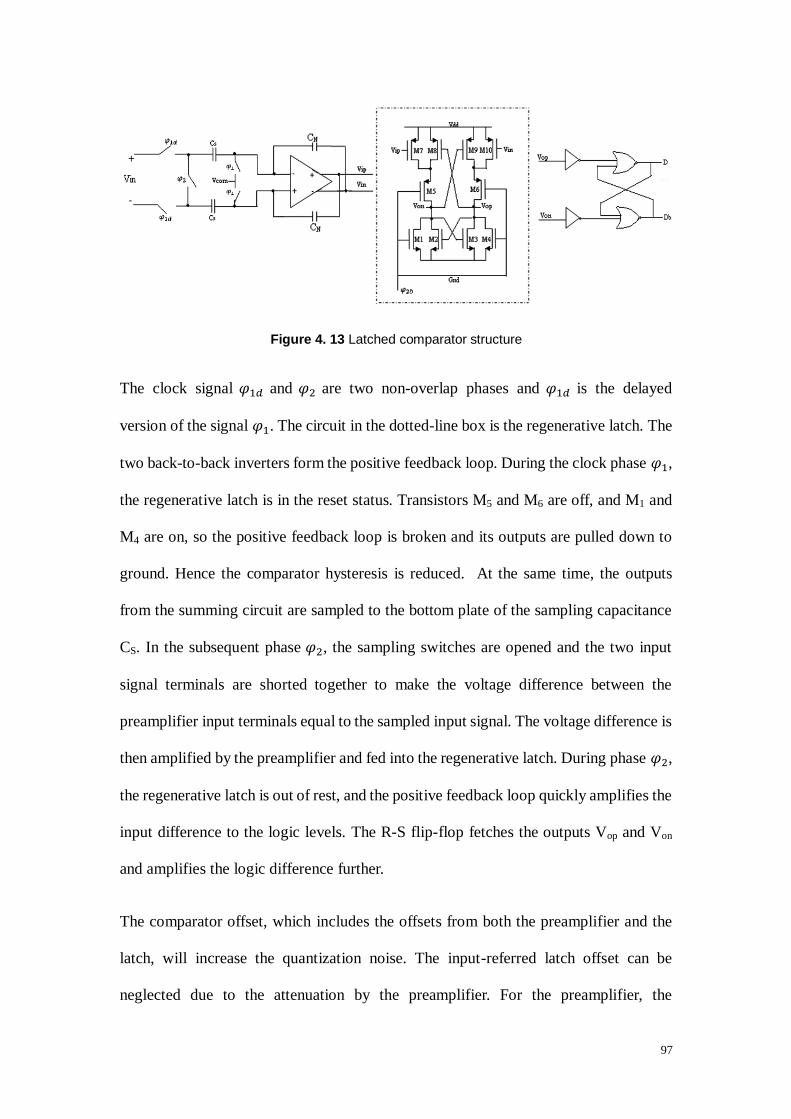
97
Figure 4. 13 Latched comparator structure
The clock signal and are two non-overlap phases and is the delayed
version of the signal . The circuit in the dotted-line box is the regenerative latch. The
two back-to-back inverters form the positive feedback loop. During the clock phase ,
the regenerative latch is in the reset status. Transistors M5 and M6 are off, and M1 and
M4 are on, so the positive feedback loop is broken and its outputs are pulled down to
ground. Hence the comparator hysteresis is reduced. At the same time, the outputs
from the summing circuit are sampled to the bottom plate of the sampling capacitance
CS. In the subsequent phase , the sampling switches are opened and the two input
signal terminals are shorted together to make the voltage difference between the
preamplifier input terminals equal to the sampled input signal. The voltage difference is
then amplified by the preamplifier and fed into the regenerative latch. During phase ,
the regenerative latch is out of rest, and the positive feedback loop quickly amplifies the
input difference to the logic levels. The R-S flip-flop fetches the outputs Vop and Von
and amplifies the logic difference further.
The comparator offset, which includes the offsets from both the preamplifier and the
latch, will increase the quantization noise. The input-referred latch offset can be
neglected due to the attenuation by the preamplifier. For the preamplifier, the

98
dimension of the input differential-pair transistors has to be enlarged to minimize its
input offset. However, the large transistor size causes big parasitic capacitances Cp at
the preamplifier input nodes. In this case, during phase , the voltage difference at the
preamplifier input nodes and is derived as given by Equation (4.22).
(4.22)
As mentioned in Section 4.4, the speed of the summing circuit is affected by the
distributed capacitances across the resistor ladder, of which the sampling capacitance
from the quantizer is the main component. Therefore, the value of CS has to be
minimized to speed up the current adder. However, the right side of Equation (4.22)
will become even smaller and the preamplifier input signal will be significantly
attenuated. The effective gain of the amplifier is reduced as a result. To solve this
problem, two neutralization capacitors are added to cancel the effect from the
parasitic capacitances.
The comparator is the core of the quantizer. In the following sections, the
characteristics of the latched comparator are discussed in detail.
4.5.1 Comparator Kick-back effect
The latched comparator regenerates the input signal to a full scale digital level.
However, the high voltage level variations at the regeneration nodes may be coupled to
the comparator inputs through the parasitic capacitances of the transistors and hence
disturb the input voltage levels. This phenomenon is referred to as kick-back effect
[57]. The solutions to this problem have already been proposed in some papers [57-58].
One of the most common solutions is to add a preamplifier before the comparator.

99
Although the amplifier increases the power consumption, the kick-back effect is
suppressed significantly and the input-referred comparator offset is also reduced.
Meanwhile, the speed of the system can be improved. In this design, the preamplifier
uses exactly the same topology as that for the RC- integrator, but the sizes of the input
differential pair transistors are enlarged to minimize the input-referred offset. The gain
of this stage does not need to be very high, as 10 to 20 is enough to suppress the
kick-back effect and the input-referred latch offset. In addition, transistors M5 and M6
in the regeneration circuit also isolate the input signals from the regenerative output
nodes. Therefore, the kick-back effect is reduced even further.
4.5.2 Clock Feed-Through Effect
During the reset phase, clock signal is used to break the positive feedback loop and
bring the differential nodes of the comparator to ground. Therefore, the comparator
hysteresis is reduced effectively. However, this signal also introduces clock
feed-through effect through the transistor parasitic capacitances, as shown in Figure
4.14. The regenerative node output signal is shown in Figure 4.15, where the sharp
glitches are due to the clock feed-through effect, as marked by the label.
Figure 4. 14 feed-through effects from the parasitic capacitance
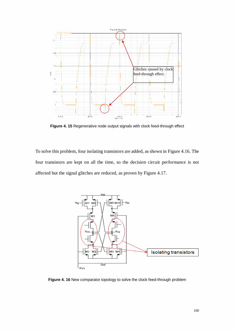
100
Figure 4. 15 Regenerative node output signals with clock feed-through effect
To solve this problem, four isolating transistors are added, as shown in Figure 4.16. The
four transistors are kept on all the time, so the decision circuit performance is not
affected but the signal glitches are reduced, as proven by Figure 4.17.
Figure 4. 16 New comparator topology to solve the clock feed-through problem
Glitches caused by clock
feed-through effect.

101
Figure 4. 17 Regenerative node output signals with clock feed-through effect reduced
4.5.3 Comparator Offset
Due to the circuit asymmetries and parasitizes, the comparator exhibits input-referred
offset. The offset is measured as the difference between the input point of Vdd/2 and the
point where Vout is at Vdd/2. As stated in Section 4.5.1, besides suppressing the
kick-back effect, the preamplifier also reduces the comparator input-referred offset. In
this design, the DC gain of the preamplifier is set at 27dB, which is high enough to
attenuate the input-referred offset. As shown in Figure 4.18, the offset of the designed
comparator is around 70µV. It is quite small comparing to the multi-bit quantizer step
size and can be neglected.

102
Figure 4. 18 Comparator offset measurement
4.5.4 Comparator performance
With the negative input set at Vdd/2, a pulse is applied at the positive input of the
comparator. The output of the comparator is shown in Figure 4.19. It is easy to observe
that besides the glitches caused by the clock feed-through effect, there are also other
glitches. These glitches are introduced when signal transition takes place at the
regenerative latch output nodes. Since sufficient time is allocated for the decision
circuit to make signal transitions and the glitch peaks are very small, these glitches will
not affect the comparator outputs.
Comparator offset

103
Figure 4. 19 Comparator output with input pulses
Figure 4.20 shows the output of the comparator when a differential sinusoidal signal is
applied at the input. As can be observed, the output changes its pulses according to the
input signal amplitudes.
Figure 4. 20 Comparator output with differential sinusoidal input signal

104
4.6 Feedback DAC Design
As shown in Figure 4.1, two current steering non-return-to-zero (NRZ) DACs are used
in this modulator. The first one, DAC1, converts the 15-bit thermometer code output to
the analog current signal and feeds it to the loop filter input, which forms a negative
feedback loop. In this manner, the quantizer output estimates the modulator input. The
second one, DAC2, is directly connected to the quantizer input to compensate the
one-period delay, as explained in Section 3.1.2.2.
The topology for DAC1 is shown in Figure 4.21 on the next page. The output from the
DAC is fed to the input of the RC-integrator Op Amp. A pair of current sources is also
connected to the same point to maintain the common-mode voltage level at the Op Amp
input. The current in each source is given by the following equation.
(4.23)
where IDAC1 stands for the current in each source and Idac1 is the DAC unit cell current.
As can be observed from the figure, each current cell of the DAC is composed of four
transistors. The current source transistor M1 supplies current for the cell. M2 is a
cascode transistor to increase the output impedance of the current source and prevent
the dynamic glitches at the source noded of M3 and M4 from impacting the current in
M1. The two switch transistors M3 and M4 are controlled by the complementary digital
codes Di and Dib respectively.
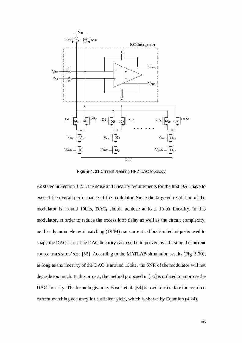
105
Figure 4. 21 Current steering NRZ DAC topology
As stated in Section 3.2.3, the noise and linearity requirements for the first DAC have to
exceed the overall performance of the modulator. Since the targeted resolution of the
modulator is around 10bits, DAC1 should achieve at least 10-bit linearity. In this
modulator, in order to reduce the excess loop delay as well as the circuit complexity,
neither dynamic element matching (DEM) nor current calibration technique is used to
shape the DAC error. The DAC linearity can also be improved by adjusting the current
source transistors‟ size [35]. According to the MATLAB simulation results (Fig. 3.30),
as long as the linearity of the DAC is around 12bits, the SNR of the modulator will not
degrade too much. In this project, the method proposed in [35] is utilized to improve the
DAC linearity. The formula given by Bosch et al. [54] is used to calculate the required
current matching accuracy for sufficient yield, which is shown by Equation (4.24).

106
(4.24)
For DAC linearity of 12bits, the current matching variation should not be larger than
0.6%. Then the current source transistors (M1, M5…M57) of DAC1 are designed
according to the Pelgrom model given in [55].
(4.25)
where Aβ and AVt are the technology constants, W and L are the width and length of the
current source transistor and (VGS -VTH) is the overdrive voltage of the transistor. In this
design, the current source transistors are adjusted to have large overdrive voltages to
guarantee the required current matching accuracy.
Since the second feedback DAC is connected to the quantizer input, any nonidealities
from this stage will be suppressed by the gain of the loop filter. Therefore, the noise and
linearity requirements on DAC2 are relaxed quite a lot. For easy interface with the
summing circuit, the current cells of DAC2 are implemented using PMOS transistors
with the similar structure as that of DAC1.
4.7 D Flip-Flop (DFF)
As depicted in the system level design and shown in Figure 4.1, a one-period delay is
inserted to absorb the excess loop delay caused by the quantizer, the DAC and the loop
filter. A commonly used DFF is implemented to realize the one-period delay in this
design, as shown in Figure 4.22. The DFF is composed of eight two-input NAND gates
and one inverter. It is triggered by the negative edge of the clock signal CLK.

107
Figure 4. 22 D flip-flop topology
The outputs from the DFF are used to control the feedback DACs. With a square wave
input, the output from the DFF is shown in Figure 4.23 below. As can be observed from
this figure, the output Q changes its status only when the clock edge falls.
Figure 4. 23 DFF output with square wave input signal
The clock signals used to control the DFF and the quantizer are produced by an ideal
clock generator, as shown in Figure 4.24.
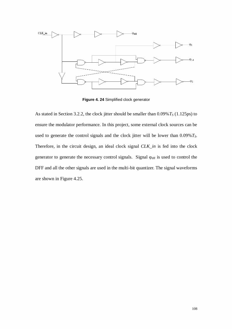
108
Figure 4. 24 Simplified clock generator
As stated in Section 3.2.2, the clock jitter should be smaller than 0.09%TS (1.125ps) to
ensure the modulator performance. In this project, some external clock sources can be
used to generate the control signals and the clock jitter will be lower than 0.09%TS.
Therefore, in the circuit design, an ideal clock signal CLK_in is fed into the clock
generator to generate the necessary control signals. Signal φdff is used to control the
DFF and all the other signals are used in the multi-bit quantizer. The signal waveforms
are shown in Figure 4.25.

109
Figure 4. 25 Clock signal waveforms
4.8 Summary of Chapter 4
In this chapter, the circuit designs of various blocks are discussed in detail.
The first integrator is implemented using the RC-integrator structure due to its high
requirement on the linearity. The folded-cascode topology is used for the Op Amp (Fig.
4.2), as it is more suitable for low supply designs. The common-mode feedback (CMFB)
circuit is also included to maintain the output common-mode voltage level of the
differential Op Amp. The DC gain of the Op Amp is boosted up to 40dB and the GBW
is around three times of the sampling rate (fS), both satisfy the requirements set in
Chapter 3.

110
For the second to fifth integrators, the GmC-integrator structures are used for their
superior speed performance. Source degenerated transconductors are used to improve
the linearity (Fig. 4.7). Since all the subsequent integrators use the similar
transconductor topology, only the design of the second one is shown in detail in this
chapter. The size of the current source transistors are adjusted to give the best tradeoff
between the noise performance and the output signal swing. Generally, the design of the
integrators and transconductors meet the requirements set in the MATLAB simulations,
as shown in Table 4.1.
The current summing operation is realized by a fast and low-power active current adder,
as shown in Figure 4.11. The resistance values of the resistor ladder are optimized to
give the best tradeoff between the modulator speed and the input dynamic range.
The multi-bit quantizer consists of fifteen latched comparators. In the latched
comparator, the preamplifier is used to suppress the kick-back effect at the regenerative
circuit output nodes. The comparator input-referred offset is reduced at the same time.
Four isolating transistors are also added to reduce the clock feed-through effect. In
general, the performance of the multi-bit quantizer is sufficiently good for this design.
Two current steering feedback DACs are used in the modulator. For the first DAC, the
linearity must be higher than that of the whole system (10bits). The current source
transistors‟ sizes of the DAC are adjusted according to the Bosch et al. formula [54] and
the Pelgrom model [55]. Finally, this DAC can achieve a linearity of round 12bits,
which satisfies the requirement set in the MATLAB simulations. For the second DAC,
the linearity requirement is not so stringent, because any nonidealities of this stage will
be attenuated by the loop filter.
A common DFF is used to insert the one-period delay to absorb the excess loop delay.

111
Since some external clock sources can be utilized to generate the clock signal with jitter
error lower than 0.09%TS, an ideal clock generator is used to produce the control
signals for various blocks in the circuit level design.
The modulator circuit level performance is evaluated in the subsequent chapter.

112
Chapter 5
Results and Discussions
5.1 Circuit Level Simulation Results
With the circuits for various components designed to satisfy the performance
requirements, simulations are performed to check the overall modulator performance.
All the circuit components are cascaded and the top level schematic is shown in Figure
5.1. The Cadence Virtuoso Spectre Circuit Simulator is used to perform the
simulations.
To check the performance of the modulator, input signals with both low and high
frequencies are tested with transient simulations. The transient simulation time is set at
11.49 µS and 9192 output points are generated in total. After the simulation completed,
the output bit streams are transferred to MATLAB to generate the SNR and PSD plots.
For both simulations, the first 1000 output points are not used, because the modulator is
preparing for stable operation during that time. For the low frequency testing, it is
always necessary to include some harmonic distortions in the calculation of SNDR.
Hence, a signal with the frequency of 3.90625MHz is used. Therefore, the harmonic
distortions up to twelfth-order will fall in the signal band and be counted in the SNDR
calculation. For the high frequency testing, the signal frequency is set at
49.8046875MHz. For both input signal frequencies, the SNR curves are plotted and
compared with those from the modulator system level simulations, as shown in Figure
5.2 and 5.3 respectively.

113
Figure 5. 1 Modulator circuit topology by cascading all the block components
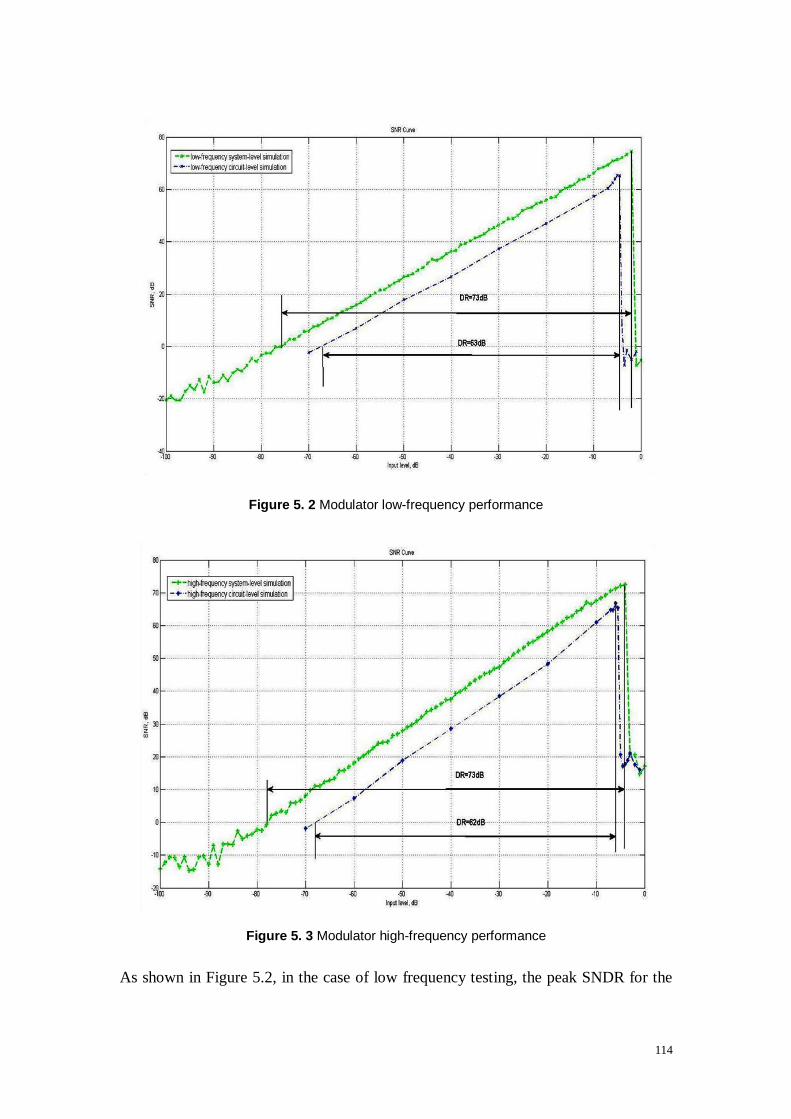
114
Figure 5. 2 Modulator low-frequency performance
Figure 5. 3 Modulator high-frequency performance
As shown in Figure 5.2, in the case of low frequency testing, the peak SNDR for the

115
modulator system level model is around 74dB and occurs at the input of -3dB of full
scale (-3dBFS). The dynamic range for the ideal modulator is about 73dB. While for
the circuit level simulation, the modulator becomes unstable when the input is higher
than -5dBFS and the peak SNDR is around 64dB. The dynamic range is about 63dB,
which is about 10dB lower than that of the system level simulation. For the high
frequency system level testing, the peak SNR is around 73dB and occurs at around
-4dBFS, which is quite reasonable for a high frequency input signal. The dynamic
range is around 73dB. However, it is observed that in the circuit level simulation, the
maximum affordable input level is -6dBFS and the peak SNR decreases to 65dB. The
dynamic range also reduces by around 11dB, as shown in Figure 5.3. To investigate the
cause of the SNDR degradation, the modulator output PSDs at the peak SNDRs for
both frequencies are plotted, as shown in Figure 5.4 and 5.5 respectively.
Figure 5. 4 Modulator low-frequency PSD plot

116
Figure 5. 5 Modulator high-frequency PSD plot
As observed from the figures, the main cause of the circuit level SNR degradation is the
higher in-band noise comparing to the system level one. For the low frequency testing,
a third-order harmonic distortion occupies a large amount in the noise band, which
significantly decreases the SNDR of the modulator. The harmonic distortion is mainly
due to the limited integrator linearity.

117
5.2 Modulator Performance Summary
Finally, the modulator performance is summarized in the table below.
Table 5. 1 Modulator performance summary with low-frequency input
Specifications Values
Dynamic Range 63dB
ENOB 10bits
Peak SNR 64dB
Maximum Input Level -6dBFS
Power Consumption
Total: 27.7mW
Integrators: 22.195mW
Multi-bit quantizer: 4.164mW
DAC: 0.198mW
Biasing circuit and other
circuit components: 1.1424mW
FOM 0.24 pJ/conv.
The modulator performance is also compared with the previously referred publications
in Table 2.1. As shown in Table 5.2, the modulator performance is not the best of them,
but still near the top.

118
Table 5. 2 Performance comparison between reported designs and this delta-sigma modulator
Reference Architecture DR
(dB)
ENOB
(Bits)
BW
(MHz)
Power
(mW)
FOM
(pJ/conv.)
[7] 5th-order,CIFF 87 14 10 100 0.273
[31] 3rd
-order,CIFF 60 9 20 10.5 0.319
[32] 3rd
-order,CIFB 54 8 10 5.5 0.55
[33] 2nd
-order,CIFB 45 7 62.5 10.8 0.63
[34] 2nd
-order,CIFB 86 14 10 40 0.12
[35] 5th-order,CIFF 75 12 25 16.4 0.069
[36] 5th-order,CIFF 55 8 25 18 1.11
[37] 3rd
-order,CIFB 72 11 10 7.5 0.115
[38] 3rd
-order,CIFB 80 13 20 20 0.122
[39 3rd
-order,CIFB 67 10 10 6 0.164
[40] 3rd
-order,CIFB 55 8 20 103 5.6
This work 5th-order,CIFF 63 10 50 27.7 0.24

119
Chapter 6
Conclusions
6.1 Conclusions
Continuous-time (CT) delta-sigma ADCs are getting popular in wireless applications
due to their low power potential for the battery-powered wireless devices. In contrast to
the discrete-time (DT) delta-sigma modulator, whose speed is limited by the Op Amp
gain bandwidth product, the CT delta-sigma modulator has less stringent gain
bandwidth requirement and hence could operate at a higher sampling frequency. The
CT modulator is also able to provide an inherent anti-aliasing filter. Recently several
researchers have reported the CMOS CT delta-sigma modulators achieving signal
bandwidth of more than 20MHz with around 10-bit resolution. It is believable that the
advancement of the CMOS process technology will continue to push up the sampling
frequency and signal bandwidth of the CT delta-sigma modulator.
In this project, the working principle and various architectures of the delta-sigma
modulator are reviewed. As an important analog-to-digital interface, the delta-sigma
modulator relaxes the strict requirements on the analog circuit design by shifting part of
the signal processing burden to the digital domain. With the oversampling and noise
shaping techniques, the delta-sigma modulator enables the implementation of
multi-standard analog-to-digital converters (ADC). These ADCs cover a wide range of

120
resolutions and signal bandwidths by providing tradeoffs in resolution and
oversampling ratio.
Continuous-time delta-sigma modulators, as the counterpart of the DT modulators, are
becoming more and more popular due to their advantages of high conversion speed and
low power consumption. The benefits provided by the CT delta-sigma modulator, such
as the implicit anti-aliasing filter and the noise-shaped sample-and-hold error, are also
discussed in detail. The method to convert a DT delta-sigma modulator to its equivalent
CT counterpart is introduced briefly. Some previous publications on the CT delta-sigma
modulators are reviewed as well.
The design procedure of the CT delta-sigma modulator starts from the selection of the
modulator architecture. The MATLAB delta-sigma design toolbox is used to perform
the system level synthesis. The system level simulation results are analyzed and
compared to determine the modulator structure and order. Various nonidealities are
checked and methods are also proposed to reduce their effects on the modulator
performance. The block coefficients got from the MATLAB simulations are used as
references for the circuit component design. The circuit level design is carried out in the
Cadence Virtuoso Analog Design Environment. Incorporating those coefficients, the
desired integrator transfer functions are derived and converted into the implementation
requirements. The integrator biasing conditions are properly adjusted, so that the
integrators‟ performances are better than meeting the requirements. The design of the
summing circuit and the multi-bit quantizer are also presented in detail. Special
121
attention is paid to minimize the parasitic capacitances while not affect the modulator
dynamic range. To absorb the excess loop delay, a one-period delay, which is
implemented using the DFF, is added in the loop filter. Besides the feedback DAC in
the loop filter, one more current steering DAC is inserted just before the multi-bit
quantizer to compensate the added delay and make the impulse response of the loop
filter equivalent to its DT counterpart. The transistors‟ sizes of the DAC current cells
are optimized to solve the matching problems.
Finally, with all the circuit blocks designed and adjusted to meet the system level
requirements, the modulator is constructed by cascading all the circuit components.
The modulator performance is evaluated and compared with that of an ideal model.
Generally, the circuit level performance of the modulator degrades by around 10dB
comparing to that of the ideal model. However, the modulator performance still meets
the design target. The tolerable input signal bandwidth is as high as 50MHz. The
dynamic range of the modulator is 63dB and the ENOB is around 10bits. The total
power consumption of the modulator is around 27.7mW and the FOM is only 0.24
pJ/conv. Therefore, the designed modulator is suitable for the next generation wireless
communications.
6.2 Future works
Generally, the designed modulator satisfies the requirements for the next generation
wireless communications. However, there is still some space to improve this work.

122
The dynamic range of the modulator is around 10dB lower than that of the
MATLAB model. The main cause of the degradation is the higher in-band noise and
the obvious third-order harmonic distortion, which are mainly induced by the
integrator nonidealities, such as the finite DC gain and the limited linearity.
Therefore, to make the loop filter approximate the ideal one, the gain-boosting
topology can be added to the integrator output and the subsequent stages of the
integrators can be implemented using RC-integrators instead.
The number of quantizer levels can also be increased to improve the dynamic range.
One constrain to the quantizer level is the power consumption, which is
proportional to the number of quantizer levels. In order to reduce the power
consumption, some techniques such as the tracking-ADC-quantizer [59] can be
used to reduce the number of comparators needed. The power consumption of the
whole modulator will also be reduced a lot.
Some more advanced techniques, such as the CMOS 45nm process, can be used if
available. The sampling clock rate and the OSR will be increased further. The
aggressiveness of the noise shaping and the number of quantizer levels can also be
reduced subsequently, which is desirable for low-power designs.
The layout design and the physical verification of the whole modulator will be
carried out when there is a tape out opportunity.

123
Publications
[1] Qiu, X., Siek, L. and Tiew, K.T., “System level design of a delta-sigma modulator
target for next generation wireless application” IEEE international symposium on
radio-frequency integration technology.
References
[1] Inose, H., Yasuda, Y., Murikami, J.,“A telemetering system by code modulation–ΣΔ
modulation,” IRE Trans.SpaceElectron.Telemetry SET-8, pp. 204–209, 1962.
[2] Candy, J.C., “A use of double integration in Sigma-Delta modulation,” IEEE trans.
Commun, vol. 33, pp. 249–258, 1985.
[3] Engels, M. (Ed.), Wireless OFDM systems, Norwell, MA: Kluwer Academic
Publishers, 2002.
[4] Schoofs, R., Deveugele, J., & Steyaert, M, Dedicated AD/DA topologies for
wireless applications, international Microwave Symposium. Fort Worth, TX,2004.
[5] Shiang Shul Yun, Sup Song Bang, Bacranial Kantilal, “A 65nm CMOS CT ΔΣ
modulator with 81dB DR and 8MHz BW auto-tuned by pulse injection”, ISSCC
2008/SESSION27/∆Σ DATA CONVERTERS/27.7, 500-503.
[6] Yang Wenhua, Schofield William, Shibata Hajime, Korrapati Sudhir, Shaikh Ali,

124
Abaskharoun Nazmy, Ribner Dave, “A 100mW 10MHz-BW CT ΔΣ modulator with
87dB DR and 9ldBc IMD”, ISSCC 2008/SESSION27/∆Σ DATA CONVERTERS/27.6,
498-500.
[7] Yan, S., Sánchez-Sinencio, E, “A continuous-time delta-sigma modulator with
88-dB dynamic range and 1.1-MHz signal bandwidth”, IEEE J. Solid-State Circuits,
vol.39(1), pp.75–86, 2004.
[8] Aziz, P. M., Sorensen, H. V., Van der Spiegel, J., “An overview of sigma-delta
converters,” IEEE Signal Processing Magazine, vol. 13 pp.61-84, 1996.
[9] Baird, R. T. and Fiez, T. S., “A low oversampling ratio 14-b 500-kHz ΔΣ ADC with
a self-calibrated multibit DAC”, IEEE J. Solid-State Circuits, vol. 31, pp. 312-320,
March 1996.
[10] Chen, F. and Leung, B. H., “A high resolution multibit sigma-delta modulator with
individual level averaging”, IEEE J. Solid-State Circuits, vol. 30, pp. 453-460,
Apr.1995.
[11] Yasuda, A., Tanimoto, H. and Iida, T., “A third-order Δ-Σ modulator using
second-order noise-shaping dynamic element matching”, IEEE J. Solid-State Circuits,
vol.33, pp.1879-1886, Dec.1998.
[12] Groeneveld, D. W. J., Schouwenaars, H. J., Termeer, H. A. H., and Bastiaansen, C.
A. A., “A self-calibration technique for monolithic high-resolution D/A converters”,
IEEE J. Solid-State Circuits, vol. 24, no. 6, pp.1517-1522, Dec.1989.

125
[13] Nam, K., Lee, S-M., Su, D.K., and Wooley, B.A., “A low-voltage low power
sigma-delta modulator for broadband analog-to-digital conversion,” IEEE J.
Solid-State Circuits, vol.40, no.9, pp.1855–1864, 2005.
[14] Brooks, T. L., Robertson, D. H., . Kelly, D. F, Muro, A. D., and Harston, S. W., “A
cascaded sigma-delta pipeline A/D converter with 1.25 MHz signal bandwidth and 89
dB SNR,” IEEE J. Solid-State Circuits, vol. 32, no. 12, pp. 1896–1906, 1997.
[15] Jiang, R. and Fiez, T., “A 14-bit delta-sigma ADC with 8X OSR and 4-MHz
conversion bandwidth in A 0.18μm CMOS process,” IEEE J.Solid-State Circuits, vol.
39, no. 1, pp. 63–74, Jan. 2004.
[16] Bosi, A., Panigada, A., Cesura, G., and Castello, R., “An 80 MHz 4x oversampled
cascaded ∆Σ-pipelined ADC with 75 dB DR and 87 dB SFDR,” in IEEE ISSCC Dig.
Tech. Papers, pp.174–175, 2005.
[17] Candy, J.C., Ninke, W.H. and Wooley, B.A., “A per-channel A/D converter having
15-segment u-255 companding,” IEEE Trans. Commun. vol. 24, pp.33–42, 1976.
[18] Koch, R., Heise, B., Eckbauer, F., Engelhardt, E., Fischer, J.A. and Parzefall, F, “A
12-bit sigma-delta analog-to-digital converter with a 15-MHz clock rate,” IEEE J.
Solid-State Circuits vol. 21, pp. 1003–1009, 1986.
[19] Gerfers, F., Ortmanns, M. and Manoli, Y., “A 12-bit power efficient
continuous-time ΣΔ modulator with 220 μW power consumption,” Proc. Eur.
Solid-State Circuits Conf., pp. 536–539, 2001.

126
[20] Van der Zwan, E.J. and Dijkmans, E.C., “A 0.2-mW CMOS ΣΔ modulator for
speech coding with 80 dB dynamic range,” IEEE J. Solid-State Circuits vol. 31, 1996.
[21] Cherry, J.A., Snelgrove, W.M., Continuous-time Delta-Sigma Modulators for
high-speed A/D Conversion, Chapter 3 Kluwer Academic Publisher, Dordrecht 1999.
[22] Jensen, J. F., Raghavan, G., Cosand, A. E., and Walden, R. H., “A 3.2-GHz
second-order delta-sigma modulator implemented in InP HBT technology,” IEEE
J.Solid-State Circuits, vol. 30, no. 10, pp. 1119-1127, Oct. 1995.
[23] Schreier, R., Zhang, B., “Delta-sigma modulators employing continuous-time
circuitry,” IEEE Trans. Circuits Syst. I, vol.43, pp.324–332, 1996.
[24] Shoaei, O., Continuous-time delta-sigma A/D converters for high speed
applications, PhD Thesis, Carleton University, 1995.
[25] Gregorian, R., Temes, G.C., Analog MOS Integrated Circuits for Signal
Processing, John Willey & Sons, 1986.
[26] Gardner, F.M., “A transformation for digital simulation of analog filters,” IEEE
Trans. Commun.vol.34, pp.676–680, 1986.
[27] Das, A., Hezar, R., Byrd, R., Gomez, G., Haroun, B., “4th-order 86 dB CT ΣΔ
ADC with two amplifiers in 90 nm CMOS,” Proc. IEEE Int. Solid-State Circuits Conf.
pp. 496–497, 2005.
[28] Benabid, S., Aghdam, E.N., Benabes, P., Guessab, S. and Kielbasa, R., “CMOS

127
design of a multibit band-pass continuous-time sigma delta modulator running at 1.2
GHz,” Proc. IEEE Int. Caracas Conf. Devices, Circuits Syst., pp. 51–55, 2004.
[29] Schreier, R., Lloyd, J., Singer, L., Paterson, D., Timko, M., Hensley, M., Patterson,
G., Behel, K., Zhou, J. and Martin, W.J., “A 50mW bandpass ΣΔ ADC with 333 kHz
BW and 90 dB DR,” Proc. IEEE Int. Solid-State Circuits Conf. pp. 216–217, 2002.
[30] Van der Zwan, E.J., “A 2.3mW CMOS ΣΔ modulator for audio applications,”
IEEE J. Solid-State Circuits, pp.220–221, 1997.
[31] Vijay Dhanasekaran, Manisha Gambhir, Mohamed M. Elsayed, Edgar
Sánchez-Sinencio, Jose Silva-Martinez, Chinmaya Mishra, Lei Chen, Erik Pankratz,
“20MHz BW 68dB DR CT ΔΣ ADC based on a multi-bit Time-domain quantizer and
feedback element”, IEEE International solid-state circuits conference, 8-12 Feb 2009,
174-175.
[32] Ramy Yousry, Emad Hegazi, Member, IEEE, and Hani F. Ragai, Member, IEEE,
“A 3rd-order 9-bit 10-MHz CMOS ∆Σ modulator with one active stage,” Circuits and
Systems I: Regular Papers, IEEE Transactions on Circuits and Systems I: Fundamental
Theory and Applications, 31 Oct 2008, 2469-2482.
[33] Arias, J., Quintanilla, L., Enríquez, L., Hernández-Mangas, J., Vicente, J.,
Segundo, J., “A 1-GHz, multibit, continuous-time, delta–sigma ADC for Gigabit
Ethernet,” Microelectronics Journal, vol.39, Dec 2008, 1642-1648.
[34] Matthew Z. Straayer and Michael H. Perrott, “A 12-bit, 10-MHz bandwidth,
128
continuous-time sigma delta ADC with a 5-Bit, 950-MSper s VCO-based quantizer,”
IEEE Journal of Solid-State Circuits 43 (4), pp. 805-814.
[35] Chen Fang, Kuendiger Till, Erfani Shervin and Ahmadi Majid, “Design of a
wideband low-power continuous-time ΣΔ modulator in 90 nm CMOS technology,”
Analog Integrated Circuits and Signal Processing 54 (3), pp. 187-199.
[36] Chen Xuefeng , Wang Yan , Fujimoto Yoshihisa, Pascal Lo Ré , Kanazawa Yusuke,
Steensgaard Jesper , and Temes Gábor, “A 18mW CT ∆Σ Modulator with 25MHz
Bandwidth for Next Generation Wireless Applications,” Proceedings of the Custom
Integrated Circuits Conference, art. no. 4405684, pp. 73-76.
[37] Raf Schoofs, Michiel S. J. Steyaert and Willy M. C. Sansen, “A design-optimized
continuous-time delta–sigma ADC for WLAN applications,” IEEE Transactions on
Circuits and Systems I: Regular Papers 54 (1), pp. 209-217.
[38] Mitteregger Gerhard, Ebner Christian, Mechnig Stephan, Blon Thomas, Holuigue
Christophe and Romani Ernesto, “A 20-mW 640-MHz CMOS continuous-time ADC
with 20-MHz signal bandwidth, 80-dB dynamic range and 12-bit ENOB,” IEEE
Journal of Solid-State Circuits 41 (12), pp. 2641-2649.
[39] Schoofs Raf, Eeckelaert Tom, Steyaert Michiel, Gielen Georges and Sansen Willy,
“A continuous-time delta-sigma modulator for 802.11abg WLAN implemented with a
hierarchical bottom-up optimization methodology,” Proceedings of the IEEE
International Conference on Electronics, Circuits, and Systems, art. no. 4263525, pp.

129
950-953.
[40] Trevor C. Caldwell and David A. Johns, “A time-interleaved continuous-time
delta-sigma modulator with 20-MHz signal bandwidth,” IEEE Journal of Solid-State
Circuits 41 (7), art. no. 1644868, pp. 1578-1588.
[41] Ranjbar. M., Mehrabi.A., Oliaei.O., “Continuous-time feedforward sigma-delta
modulators with robust signal transfer function,” In Proc.Int. Symp. Circ. Syst, 2008, pp.
1878-1881.
[42] Schreier R., The Delta-Sigma Toolbox 5.1,. http://www.mathworks.com/, 2000.
[43] Phillps, K., Nuijten, P., Roovers, R., Munoz, F., Tejero, M., Torralba, A., “A 2mW
89dB DR continuous-time ΣΔ ADC with increased wide-band interference immunity,”
ISSCC Digest of Technical Papers, Feb. 2004, pp. 86-87.
[44] Cherry, J. A. and Snelgrove, W. M., “Excess loop delay in continuous-time
delta-sigma modulator,” IEEE Trans. Circuits & System II, vol. 46, pp. 376-389, Apr.
1999.
[45] Gao, W., Shoaei, O., Snelgrov, W. M., “Excess loop delay effects in
continuous-time delta-sigma modulators and the compensation solutions,” In Proc.Int.
Symp. Circ. Syst, vol. 1, 1997, pp. 65-68.
[46] Moyal, M., Groepl, M., Werker, H., Mitteregger, G. and Schambacher, J., “A
700/900mW/Channel CMOS dual analog front-end IC for VDSL with integrated

130
11.5/14.5dBm line drivers,” ISSCC Digest of Technical Papers, Feb. 2003, pp.
416-417.
[47] Schreier, R. and Temes, G. C., Understanding delta-sigma data converters.
Piscataway, NJ; Hoboken, N.J. ; Chichester: IEEE Press Wiley, 2005.
[48] Li, Z., Design of a 14-bit Continuous-Time Delta-Sigma A/D Modulator with
2.5MHz Signal Bandwidth, Ph.D. Thesis, Oregon State University, Corvallis, Oregon,
Jan. 2006.
[49] Fang, J., A comparative study of lowpass continuous-time ΔΣ modulators with
pulse shaped DACs, M.S. thesis, Oregon State University, Corvallis, Oregon, Sept.
2005.
[50] Benabid, S., Aghdam, E.N., Benabes, P., Guessab, S., Kielbasa, R., “CMOS design
of a multibit band-pass continuous-time sigma delta modulator running at 1.2 GHz,”
Proc. IEEE Int. Caracas Conf. Devices, Circuits Syst., pp. 51–55, 2004.
[51] Carley, L. R., “A noise-shaping coder topology for 15 bit converters,” IEEE J.
Solid-State Circuits, vol. SC-34, pp. 267-273, April. 1989.
[52] David A. Johns, Ken Martin, Analog Integrated Circuit Design, John Wiley &
Sons 1997.
[53] Paton, S., “A 70-mW 300-MHz CMOS continuous-time ADC with 15-MHz
bandwidth and 11bits of resolution,” IEEE J. Solid-State Circuits, vol. 39, pp.

131
1056-1063, Jul. 2004.
[54] Den Bosch, A. V., Steyaert, M., & Sansen W. (2000). “An accurate statistical yield
model for CMOS current-steering D/A converters”, In Proceedings of IEEE
International Symposium on Circuitsand Systems, Geneva, Switzeland, pp. IV
105–108.
[55] Pelgrom, M., Duinmaijer, A., & Welbers, A. (1989). “Matching properties of MOS
transistors”. IEEE Transactions on Circuits and Systems II, SC(24), 1433–1439.
[56] Soin, R. S., Maloberti, F. and Franca, J., “Analogue-digital ASICs: Circuits and
techniques, design tools and applications”, IEE Circuits and systems Series 1991 .
[57] Aizad, N., Design and Implementation of Comparator for Sigma-Delta Modulator,
Master thesis, Linköping University, Jun. 2006.
[58] Figueiredo, P. M., and Vital, J. C., “Low kickback noise techniques for CMOS
latched comparators”, ISCAS ’04. Proceedings of the 2004 International Symposium on
Circuits and Systems, vol. 1, pp.537-540, May 2004.
[59] Dorrer, L., “A 3mW 74dB SNR 2MHz CT ∆∑ ADC with a tracking-ADC
quantizer in 0.13µm CMOS”, in ISSCC Dig. Tech. Papers, pp. 492-493, Feb. 2005.

132
Appendix A
A.1 MATLAB Codes for Determining the Block Coefficients for
Delta-Sigma Modulators
%MATLAB code to calcualte the loop coefficients in the fifth-order
%CT %modulator
clear all;
close all;
digits 8;
Fs = 60e6; % Sampling Frequency
N = 5; % Order
osr=8; % Oversampling ratio
H_inf=3.5; % Maximum out-of-band gain of NTF
cd('C:\Documents and Settings\e080051\Desktop\matlab_master\OSR 5th
order\4bit_DWA\DWA\Testing');
NTF=synthesizeNTF(N,osr,1,H_inf,0);
%Hz=1-1/NTF;
Hz=1/NTF-1;
[num_dt,den_dt]=zp2tf(Hz.z:,Hz.p:,Hz.k); % DT forward loop
[num1,den1]=zp2tf(Hz.z:,Hz.p:,Hz.k);
Hz_tmp1=Hz/tf([0,1],[1],1,'Variable','z^-1'); % Hz_tmp1=H'(z)+a1/b0 in Eq. (5.5)
[num2,den2]=zp2tf(Hz_tmp1.z:,Hz_tmp1.p:,Hz_tmp1.k);
Hz_tmp2=tf(num2,den2,1,'Variable','z^-1');
Hz_new=Hz_tmp2-num1(2)/den1(1); %Hz_new=H'(z) in Eq.(5.5 and Eq.(5.6)
k=num1(2)/den1(1) % k_DAC2=a1/b0, gain of DAC2
[num3,den3]=tfdata(Hz_new,'v');
[num_ct_nrz_tmp,den_ct_nrz_tmp]=d2cm(num3,den3,1)
tf(num_ct_nrz_tmp,den_ct_nrz_tmp)
% define variables as symbols to be sovled
cf=sym('cf','positive');
k1=sym('k1','positive');
k2=sym('k2','positive');
k3=sym('k3','positive');
k4=sym('k4','positive');
k5=sym('k5','positive');
g1=sym('g1','positive');
g2=sym('g2','positive');
g3=sym('g3','positive');

133
g4=sym('g4','positive');
g5=sym('g5','positive');
gz1=sym('gz1','positive');
gz2=sym('gz2','positive');
[cf k1 k2 k3 k4 k5 g1 g2 g3 g4 g5 gz1
gz2]=solve('cf=0.5','k2=2','k4=1','gz1=1','gz2=0.1','g1=1','k1*g1=num_ct_nrz_tmp(2)','k1*k2*g2+cf*k1*k3*
g3=num_ct_nrz_tmp(3)','k1*k2*k3*g1*gz1+k1*k4*k5*g1*gz2+k1*k2*k3*g3+cf*k1*k3*k4*g4-cf*k1*k2*k3*g
2*gz1=num_ct_nrz_tmp(4)','k1*k2*k4*k5*g2*gz2+k1*k2*k3*k4*g4+cf*k1*k3*k4*k5*g5+cf*k1*k3*k4*k5*g3
*gz2=num_ct_nrz_tmp(5)','k1*k2*k3*k4*k5*g5+k1*k2*k3*k4*k5*g1*gz1*gz2+k1*k2*k3*k4*k5*g3*gz2-cf*k
1*k2*k3*k4*k5*g2*gz1*gz2=num_ct_nrz_tmp(6)','k2*k3*gz1+k4*k5*gz2=den_ct_nrz_tmp(3)','k2*k3*k4*k
5*gz1*gz2=den_ct_nrz_tmp(5)','cf','k1','k2','k3','k4','k5','g1','g2','g3','g4','g5','gz1','gz2');
%[cf k1 k2 k3 k4 k5 g1 g2 g3 g4 g5 gz1
gz2]=solve('cf=1.1857','k2=0.246','k4=1','k1=0.17','k3=0.0633','k5=0.338','k1*g1=num_ct_nrz_tmp(2)','k1
*k2*g2+cf*k1*k3*g3=num_ct_nrz_tmp(3)','k1*k2*k3*g1*gz1+k1*k4*k5*g1*gz2+k1*k2*k3*g3+cf*k1*k3*k4
*g4-cf*k1*k2*k3*g2*gz1=num_ct_nrz_tmp(4)','k1*k2*k4*k5*g2*gz2+k1*k2*k3*k4*g4+cf*k1*k3*k4*k5*g5+
cf*k1*k3*k4*k5*g3*gz2=num_ct_nrz_tmp(5)','k1*k2*k3*k4*k5*g5+k1*k2*k3*k4*k5*g1*gz1*gz2+k1*k2*k3
*k4*k5*g3*gz2-cf*k1*k2*k3*k4*k5*g2*gz1*gz2=num_ct_nrz_tmp(6)','k2*k3*gz1+k4*k5*gz2=den_ct_nrz_t
mp(3)','k2*k3*k4*k5*gz1*gz2=den_ct_nrz_tmp(5)','cf','k1','k2','k3','k4','k5','g1','g2','g3','g4','g5','gz1','gz2');
k_coeff=[eval(cf),eval(k1),eval(k2),eval(k3),eval(k4),eval(k5),eval(g1),eval(g2),eval(g3),eval(g4),eval(g5)
,eval(gz1),eval(gz2)]
cf=k_coeff(1,1);
g1=k_coeff(1,2);
g2=k_coeff(1,3);
g3=k_coeff(1,4);
g4=k_coeff(1,5);
g5=k_coeff(1,6);
gz1=k_coeff(1,7);
gz2=k_coeff(1,8);
k1=k_coeff(1,9);
k2=k_coeff(1,10);
k3=k_coeff(1,11);
k4=k_coeff(1,12);
k5=k_coeff(1,13);
%b1=0.2852
b1=-5.5;
%b1= 7;
%b1=-5.88;
num =[(num_ct_nrz_tmp(2)+g2*k2*b1) (num_ct_nrz_tmp(3)+g3*k2*k3*b1)
(num_ct_nrz_tmp(4)+g4*k4*k2*k3*b1+g2*k2*b1*gz2*k4*k5)
(num_ct_nrz_tmp(5)+g5*k4*k5*k2*k3*b1+g3*k2*k3*b1*gz2*k4*k5)];
den = [1 0 den_ct_nrz_tmp(3) 0 den_ct_nrz_tmp(5) 0] ;
[z,p,k] = tf2zp(num,den);
Lo = zpk(z,p,k)
134
%%%%%%%%%%%%%%%%%%%%%%%%%%%%%%%%%%%%%%%%%%%%%%%%%%%
figure(2); clf
f = [linspace(10^-4,10^-3,1000) linspace(10^-3,10^-2,1000) linspace(10^-3,10^-2,1000)
linspace(10^-2,10^-1,100) linspace(10^-1,1,1000) linspace(1,10,1000)];
w = 2*pi*f; s = j*w; z=exp(s);
magH2 = dbv(evalTF(NTF,z));%noise transfer function
%%magH = dbv(evalTFP(Lo,H,f));
magH1 = dbv(evalTF(Lo,s));
magH = dbv(evalTFP(Lo,NTF,f));%signal transfer function
semilogx(f,magH,'b');
xlabel('Normalized Frequency (Fs->1)');
ylabel('dB');
hold on;
semilogx(f,magH2,'g');
hold on;
semilogx(f,magH1,'r');
hold on;
grid on;
axis([10^-4 10 -100 100]);
fprintf(1,'Finish simulation.. ');
%%%%%%%%%%%%%%%%%%%%%%%%%%%%%%%%%%%%%%%%%%%%%%%%%%%
A.2 MATLAB Codes for Simulations Measuring the SNR
% SNDR computation of a general delta-sigma modulator
fin=fs*m/N;
Y = fft(y,N);
Pyy = Y.* conj(Y) / N^2;
f = fs*(0:N/2)/N;
nB= ceil(N/(2*M));
[P,n]=max(Pyy(1:round(fin/fs*N)+10));
if n==1;
Ps=0 ;
else
Ps=sum(Pyy(n-1:n+1));
end
SNDR=10*log10(Ps/(sum(Pyy(1:nB))-Ps));
%%%%%%%%%%%%%%%%%%%%%%%%%%%%%%%%%%%%%%%%%%%%%%%%%%%
A.3 MATLAB Codes for Plotting PSD
fs = 1;
Ts=1;
m=16;
fin=fs*m/N;

135
M=osr;
scale1=zeros(1,101);
scale2=zeros(1,101);
b=4;
stdv=0;
del=0.5*1/(2^b-1);
e=normrnd(del,stdv*del,1,(2^b-1));
db=3;
A=0.5*10.^(-db/20) ;
op1_GBW=2.2;
B1=1/(2*pi*op1_GBW+k1);
op2_GBW=1.5;
B2=1/(2*pi*op2_GBW+k2);
op3_GBW=1;
B3=1/(2*pi*op3_GBW+k3);
op4_GBW=0.8;
B4=1/(2*pi*op4_GBW+k4);
op5_GBW=0.8;
B5=1/(2*pi*op5_GBW+k5);
sim('opamp_testing_GBW3');
yo=y;
clear y;
y(1:N)=yo(1000:999+N);
y=y.*hann(N);
Y = fft(y,N);
Pyy = Y.* conj(Y) / N^2;
f = fs*(1:N/2)/N;
%nB= ceil(N/(2*M));
figure(1);clf;
xlabel('Normalized Frequency (Fs->1)');
ylabel('PSD(dB)');
hold on;
semilogx(f,dbp(Pyy(1:N/2)),'b','Linewidth', 0.01);
%plot(f,dbp(Pyy(1:N/2)),'b','Linewidth', 1);
hold on;
grid on;
axis([10^-4 1 -150 0]);

136