contact formation on boron doped silicon ......survive the high-temperature co-diffusion step. if...
TRANSCRIPT
CONTACT FORMATION ON BORON DOPED SILICON SUBSTRATES FROM PASSIVATING PECV-
DEPOSITED DIELECTRIC DOPING LAYERS WITH ANTI-REFLECTIVE PROPERTIES BY SCREEN-
PRINTING AG PASTES FOR HIGH-EFFICIENCY N-TYPE SILICON SOLAR CELLS
Josh Engelhardt*, Alexander Frey, Susanne Fritz, Gabriel Micard, Stefanie Riegel, Giso Hahn and Barbara Terheiden
University of Konstanz, Department of Physics, Box 676, 78457 Konstanz, Germany
*Author of correspondence: [email protected], +49-7531-88-2080
ABSTRACT: n-type silicon solar cell designs for high-efficiency commonly incorporate boron emitter formation.
PECV-deposited boron diffusion sources are an alternative to primarily used boron gas diffusion sources. CVD layers
are multi-functional allowing for diffusion of boron, surface passivation and contact formation by one single layer. In
this case, these BSG layers are applied in a co-diffused cell design for screen-printed contacts. Reaching iVOC values
of over 660 mV as ARC layers, BSG layers are shown to be capable to support the contact formation of commercial
Ag pastes to boron emitters at standard firing conditions. An analysis of the contact resistivity as well as the contact
formation by SEM is conducted to verify the high quality of the screen-printed contact.
Keywords: boron, contact, diffusion, PECVD, screen-printing
1 INTRODUCTION
High-efficiency solar cells use n-type silicon
substrates due to the higher bulk lifetime and lower
susceptibility to degradation. Furthermore, a larger
amount of processing steps is generally needed to
fabricate such type of solar cell. Expensive boron emitter
formation as well as complex metallization techniques
and cell structures are used to achieve the necessary
efficiency to be cost-efficient.
In the last years, alternative process steps have been
developed to simplify process steps. One of these were
PECV(plasma-enhanced chemical vapor)-deposited
doped layers (i.e. boron silicate glasses, BSG) enabling
co-diffusion of emitter and FSF (front surface field) or
BSF (back surface field) diffusion in one single step
without additional masking steps [1-4].
The same layer could also be used as a passivation
layer and thereby render a commonly used and costly
Al2O3/SiNx-stack obsolete. The passivation quality has to
survive the high-temperature co-diffusion step. If applied
to the front or the back (e.g. for bifaciality) it also has to
have anti-reflective, non-absorbent properties.
Furthermore, it has to allow for any form of cost-
effective metal contact formation, such as screen-
printing. Therefore, such BSG layers are multi-purpose
layers [3].
2 EXPERIMENTAL
The deposition of dielectric doping layers was
performed using an ICP(inductively coupled plasma)-
PECVD tool with a single deposition chamber. Beside
silane, carbon dioxide and diborane diluted in hydrogen
were used as reactive gases forming a comparably
carbon-free BSG (SiOx:B) layer. The n-type silicon
substrates were KOH etched and standard industrially
cleaned before deposition of doping layers with different
thicknesses. The following diffusions were carried out in
a tube diffusion furnace using a co-diffusion step
comprising of a high temperature drive-in similar to
standard boron diffusions and a subsequent low
temperature step for a POCl3 diffusion of a FSF/BSF.
Symmetrical boron emitter samples for saturation current
density j0 and implied open circuit voltage iVOC
measurements were processed alongside on FZ-Si
substrates and passivated by either the remaining SiOx:B
doping layer or a fired Al2O3/SiNx-stack deposited after
the doping layer removal.
The emitter profile and passivation parameters were
measured using electrochemical capacitance-voltage
measurement (ECV), four-point probe and a Sinton
Lifetime Tester (QSSPC) setup. The optical properties of
the doping layers were determined by ellipsometry.
All contact samples were screen-printed using
commercially available Ag and Ag/Al pastes and
subsequently fired at different set peak firing
temperatures in an IR belt furnace. The printed finger
structure was a special TLM (transfer length method)
pattern to determine the contact and sheet resistance.
Pieces of these samples were etched in HF to remove the
metal fingers and then in HCl/HNO3 to remove the
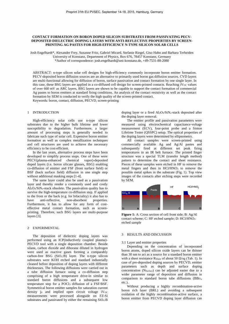
possible metal spikes in the substrate (Fig. 1). Top view
images of the contacts after etching steps were recorded
by SEM.
Figure 1: A: Cross section of cell front side; B: Ag/Al
contact scheme; C: HF etched sample; D: HCl/HNO3
etched sample
3 RESULTS AND DISCUSSION
3.1 Layer and emitter properties
Depending on the concentration of incorporated
boron atoms, doped silicon oxide layers can be thinner
than 30 nm to act as a source for a standard boron emitter
with a sheet resistance RSheet of about 50 Ω/sq (Tab. 1). In
case of pre-deposited doping sources by PECVD, emitter
parameters such as depth and surface doping
concentration (NSurface) can be adjusted easier due to a
wider parameter range of deposition and diffusion in
comparison to standard boron tube diffusions (BBr3,
etc.).
Without producing a highly recombination-active
boron rich layer (BRL) and avoiding a subsequent
oxidation of the highly recombination-active surface, a
boron emitter from PECVD doping layer diffusion can
Preprint 31th EU PVSEC, September 14-18, 2015, Hamburg, Germany

reach NSurface values above 11020 cm-3 and a depth of
more than 800 nm. This allows for low contact resistance
and a broader window of firing temperatures for proper
contact formation. In addition, the doping layers are
passivating even after the high-temperature diffusion step
[3]. In comparison, j0 values of about 80 fAcm-2 and
iVOC values of about 660 mV (Tab. I) are the same for
the remaining doping layer and a fired Al2O3/SiNx-stack
commonly used for boron emitter passivation. Optical
properties (Tab. I) of the doping layer can also be
optimized by shaping the deposition parameters. In this
case, the refractive index increases from 1.45 for
undoped layers to 1.7 at 633 nm due to incorporation of
boron atoms in the silicon oxide. Boron atoms increase
the absorption of the layer due to free carrier absorption.
Yet after the drive-in step the refraction index decreases
to 1.5 and the extinction coefficient decreases to values
below 110-4 at 400 nm due to out-diffusion of boron
atoms forming the emitter and due to changes in the
amorphous structure of the SiOx:B layer while being
exposed to high temperature during diffusion.
Arising from these properties of the doping layer, a
solar cell concept using the doping layer for surface
passivation as well as anti-reflective coating drastically
reduces the necessary production steps. Therefore, we
investigated the possibility to contact the boron emitter
through doping layers of various thicknesses and
deposition parameters by screen-printed metal paste.
Table I: SiOx:B doping layer optical and boron emitter
electrical properties. j0 and iVOC values for doping layer
and Al2O3/SiNx-stack passivation
SiOx:B layers
Thickness 30-100 nm
n @ 633 nm 1.5
k @ 400 nm <110-4
Boron emitter
RSheet 50 Ω/sq
NSurface 11020 cm-3
Depth 800 nm
j0,SiOx:B 81 fAcm-2
iVOC,SiOx:B 660 mV
j0,Al2O3/SiNx 77 fAcm-2
iVOC,Al2O3/SiNx 665 mV
3.2 Contact investigations
Ag/Al pastes are commonly used for contacting
boron doped Si by screen-printed contact finger grids.
Due to the high solubility of Al in Si, contact formation
of metal to semiconductor is facilitated [5]. With
increasing firing temperature, the specific contact
resistance (RC) decreases (Fig. 2).
The Al-Ag-Si contact formation highly depends on
the thickness of the dielectric layer in between. The
thicker it is, the higher the peak firing temperature needs
to be for the Ag/Al paste to dissolve the layer and contact
the emitter. Ag/Al pastes tend to reach very low contact
resistance values due to the comparatively deep and
therefore large inverted-pyramidal shaped contact
crystals, which are in direct contact with the Si substrate
[4, 6]. Therefore, the risk of spiking and subsequent
shunting of the space charge region is increased with
peak firing temperature. Problematic are spikes that do
not form a p+ Al emitter between the n-type Si base and
the pure metal of the spike. Fig. 3 depicts the remaining
pits after metal etching underneath the finger contact
area. From image A (arrow) to D the pits grow in
diameter as well as depth.
Figure 2: Specific contact resistance for Ag/Al paste in
dependence on the firing furnace set peak temperature for
30 and 100 nm thick doping layers
Figure 3: SEM images of areas underneath Ag/Al paste
fingers after HF etch (Cleft, Dleft) and subsequent
HCl/HNO3 etch (A, B, Cright, Dright) for increasing firing
furnace set peak temperatures according to Fig. 2
Preprint 31th EU PVSEC, September 14-18, 2015, Hamburg, Germany
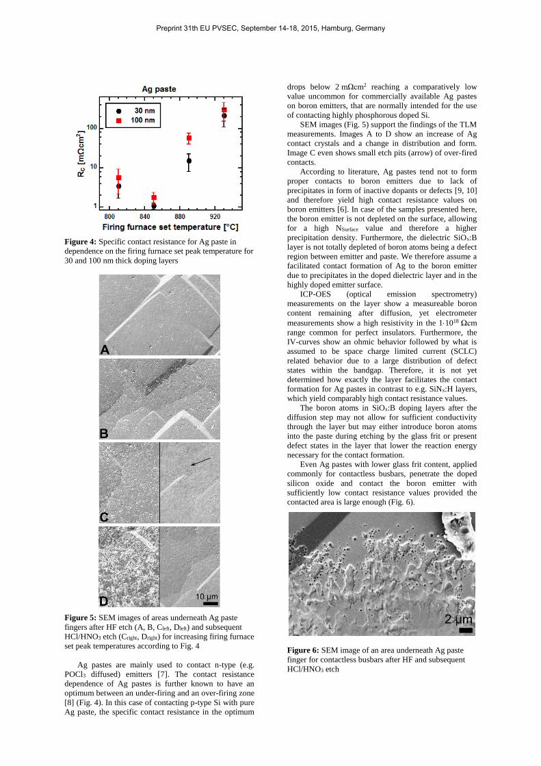
Figure 4: Specific contact resistance for Ag paste in
dependence on the firing furnace set peak temperature for
30 and 100 nm thick doping layers
Figure 5: SEM images of areas underneath Ag paste
fingers after HF etch (A, B, Cleft, Dleft) and subsequent
HCl/HNO3 etch (Cright, Dright) for increasing firing furnace
set peak temperatures according to Fig. 4
Ag pastes are mainly used to contact n-type (e.g.
POCl3 diffused) emitters [7]. The contact resistance
dependence of Ag pastes is further known to have an
optimum between an under-firing and an over-firing zone
[8] (Fig. 4). In this case of contacting p-type Si with pure
Ag paste, the specific contact resistance in the optimum
drops below 2 mΩcm2 reaching a comparatively low
value uncommon for commercially available Ag pastes
on boron emitters, that are normally intended for the use
of contacting highly phosphorous doped Si.
SEM images (Fig. 5) support the findings of the TLM
measurements. Images A to D show an increase of Ag
contact crystals and a change in distribution and form.
Image C even shows small etch pits (arrow) of over-fired
contacts.
According to literature, Ag pastes tend not to form
proper contacts to boron emitters due to lack of
precipitates in form of inactive dopants or defects [9, 10]
and therefore yield high contact resistance values on
boron emitters [6]. In case of the samples presented here,
the boron emitter is not depleted on the surface, allowing
for a high NSurface value and therefore a higher
precipitation density. Furthermore, the dielectric SiOx:B
layer is not totally depleted of boron atoms being a defect
region between emitter and paste. We therefore assume a
facilitated contact formation of Ag to the boron emitter
due to precipitates in the doped dielectric layer and in the
highly doped emitter surface.
ICP-OES (optical emission spectrometry)
measurements on the layer show a measureable boron
content remaining after diffusion, yet electrometer
measurements show a high resistivity in the 11018 Ωcm
range common for perfect insulators. Furthermore, the
IV-curves show an ohmic behavior followed by what is
assumed to be space charge limited current (SCLC)
related behavior due to a large distribution of defect
states within the bandgap. Therefore, it is not yet
determined how exactly the layer facilitates the contact
formation for Ag pastes in contrast to e.g. SiNx:H layers,
which yield comparably high contact resistance values.
The boron atoms in SiOx:B doping layers after the
diffusion step may not allow for sufficient conductivity
through the layer but may either introduce boron atoms
into the paste during etching by the glass frit or present
defect states in the layer that lower the reaction energy
necessary for the contact formation.
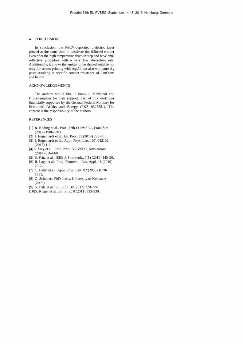
Even Ag pastes with lower glass frit content, applied
commonly for contactless busbars, penetrate the doped
silicon oxide and contact the boron emitter with
sufficiently low contact resistance values provided the
contacted area is large enough (Fig. 6).
Figure 6: SEM image of an area underneath Ag paste
finger for contactless busbars after HF and subsequent
HCl/HNO3 etch
Preprint 31th EU PVSEC, September 14-18, 2015, Hamburg, Germany
4 CONCLUSIONS
In conclusion, the PECV-deposited dielectric layer
proved at the same time to passivate the diffused emitter
even after the high temperature drive-in step and have anti-
reflective properties with a very low absorption rate.
Additionally, it allows the emitter to be shaped suitable not
only for screen-printing with Ag/Al, but also with pure Ag
paste resulting in specific contact resistance of 2 mΩcm2
and below.
ACKNOWLEDGEMENTS
The authors would like to thank L. Mahlstädt and
B. Rettenmaier for their support. Part of this work was
financially supported by the German Federal Ministry for
Economic Affairs and Energy (FKZ 0325581). The
content is the responsibility of the authors.
REFERENCES
[1] R. Keding et al., Proc. 27th EUPVSEC, Frankfurt
(2012) 1906-1911.
[2] J. Engelhardt et al., En. Proc. 55 (2014) 235-40.
[3] J. Engelhardt et al., Appl. Phys. Lett. 107, 042102
(2015) 1-4.
[4]A. Frey et al., Proc. 29th EUPVSEC, Amsterdam
(2014) 656-660.
[5] S. Fritz et al., IEEE J. Photovolt., 5(1) (2015) 145-50.
[6] R. Lago et al., Prog. Photovol.: Res. Appl. 18 (2010)
20-27.
[7] C. Ballif et al., Appl. Phys. Lett. 82 (2003) 1878-
1881.
[8] G. Schubert, PhD thesis, University of Konstanz
(2006).
[9] S. Fritz et al., En. Proc. 38 (2013) 720-724.
[10]S. Riegel et al., En. Proc. 8 (2011) 533-539.
Preprint 31th EU PVSEC, September 14-18, 2015, Hamburg, Germany