configuration encoding techniques for ... - unsw engineering
TRANSCRIPT

Configuration Encoding Techniques
for Fast FPGA Reconfiguration
Usama Malik
Bachelor of Engineering, UNSW 2002
A thesis submitted in fulfilment
of the requirements for the degree of
Doctor of Philosophy
School of Computer Science and Engineering
June 2006
Copyright c© 2006, Usama Malik

Originality Statement
‘I hereby declare that this submission is my own work and to the best of
my knowledge it contains no materials previously published or written by
another person, or substantial proportions of material which have been ac-
cepted for the award of any other degree or diploma at UNSW or any other
educational institution, except where due acknowledgement is made in the
thesis. Any contribution made to the research by others, with whom I have
worked at UNSW or elsewhere, is explicitly acknowledged in the thesis. I
also declare that the intellectual content of this thesis is the product of my
own work, except to the extent that assistance from others in the project’s
design and conception or in style, presentation and linguistic expression is
acknowledged.’
Signed ..........................................................................

Acknowledgements
I would like to thank my supervisor, Dr. Oliver Diessel, for his continuous
support in this project. Thank you for your high throughput editing, short
response time feedback and fine-grained discussions containing no null data!
Numerous other researchers have given useful feedback on this work.
Their names are, in alphabetical order, Aleksandar Ignjatovic (UNSW,
Australia), Christophe Bobda (University of Erlangen, Germany), Gareth
Lee (UWA, Australia), Professor George Milne (UWA, Australia), Gordon
Brebner (Xilinx Inc., USA), Professor Hartmut Schmeck (Karlsruhe Univer-
sity, Germany), A/Professor Hossam ElGindy (UNSW, Australia), Profes-
sor Jurgen Teich (University of Erlangen, Germany), Kate Fisher (UNSW,
Australia). A/Professor Katherine Compton (UWM, USA), Mark Shand
(Compaq Inc., France), Professor Martin Middendorf (University of Leipzig,
Germany), Peter Alfke (Xilinx Inc., USA), Philip Leong (Imperial College,
UK) and A/Professor Sri Parameswaran (UNSW, Australia).
The Australian Research Council (ARC), the School of Computer Sci-
ence and Engineering (CSE) and the National Institute of Information and
Communication Technologies Australia (NICTA) are acknowledged for pro-
viding with the funding. In particular, Professor Paul Compton (the head of
CSE), Professor Albert Nymeyer (the head of postgraduate research at CSE),
Terry Percival (Director NICTA’s research) and Professor Gernot Heiser (the
head of Embedded and Real-time Systems (ERTOS) group in NICTA) are
acknowledged for their continuous financial support for this project. The
organisers of the International Conference on Field Programmable Logic and

Applications (FPL) 2003 are acknowledged for providing the travel fund that
enabled me to present my work at the PhD poster session in Belgium.
3
Abstract
This thesis examines the problem of reducing reconfiguration time of an
island-style FPGA at its configuration memory level. The approach followed
is to examine configuration encoding techniques in order to reduce the size
of the bitstream that must be loaded onto the device to perform a recon-
figuration. A detailed analysis of a set of benchmark circuits on various
island-style FPGAs shows that a typical circuit randomly changes a small
number of bits in the null or default configuration state of the device. This
feature is exploited by developing efficient encoding schemes for configuration
data. For a wide set of benchmark circuits on various FPGAs, it is shown
that the proposed methods outperform all previous configuration compres-
sion methods and, depending upon the relative size of the circuit to the
device, compress within 5% of the fundamental information theoretic limit.
Moreover, it is shown that the corresponding decoders are simple to imple-
ment in hardware and scale well with device size and available configuration
bandwidth. It is not unreasonable to expect that with little modification
to existing FPGA configuration memory systems and acceptable increase in
configuration power a 10-fold improvement in configuration delay could be
achieved. The main contribution of this thesis is that it defines the limit of
configuration compression for the FPGAs under consideration and develops
practical methods of overcoming this reconfiguration bottleneck. The func-
tional density of reconfigurable devices could thereby be enhanced and the
range of potential applications reasonably expanded.

Contents
List of Figures x
List of Tables xiv
1 Introduction 1
1.1 Research Context . . . . . . . . . . . . . . . . . . . . . . . . . 2
1.2 Problem Background . . . . . . . . . . . . . . . . . . . . . . . 3
1.3 Thesis Contributions . . . . . . . . . . . . . . . . . . . . . . . 4
1.4 Thesis Outline . . . . . . . . . . . . . . . . . . . . . . . . . . . 7
2 Related Work and Contributions 9
2.1 Introduction . . . . . . . . . . . . . . . . . . . . . . . . . . . . 9
2.2 Partial Reconfiguration . . . . . . . . . . . . . . . . . . . . . . 9
2.3 Configuration Compression . . . . . . . . . . . . . . . . . . . . 12
2.4 Specialised Architectures . . . . . . . . . . . . . . . . . . . . . 14
2.5 Configuration Caching . . . . . . . . . . . . . . . . . . . . . . 15
2.6 Circuit Scheduling and Placement . . . . . . . . . . . . . . . . 15
2.7 Summary . . . . . . . . . . . . . . . . . . . . . . . . . . . . . 16
3 Models and Problem Formulation 17
3.1 Introduction . . . . . . . . . . . . . . . . . . . . . . . . . . . . 17
3.2 Hardware Platforms . . . . . . . . . . . . . . . . . . . . . . . 17
v
3.2.1 The device model . . . . . . . . . . . . . . . . . . . . . 18
3.2.2 The system model . . . . . . . . . . . . . . . . . . . . 26
3.3 Programming Environments . . . . . . . . . . . . . . . . . . . 31
3.3.1 Hardware description languages . . . . . . . . . . . . . 31
3.3.2 Conventional programming languages . . . . . . . . . . 37
3.4 Examples of Runtime Reconfigurable Applications . . . . . . . 38
3.4.1 A triple DES core . . . . . . . . . . . . . . . . . . . . . 39
3.4.2 A specialised DES circuit . . . . . . . . . . . . . . . . . 39
3.4.3 The Circal interpreter . . . . . . . . . . . . . . . . . . 43
3.5 Problem Formulation . . . . . . . . . . . . . . . . . . . . . . . 46
3.5.1 Motivation . . . . . . . . . . . . . . . . . . . . . . . . . 46
3.5.2 Problem statement . . . . . . . . . . . . . . . . . . . . 48
4 An Analysis of Partial Reconfiguration in Virtex 49
4.1 Introduction . . . . . . . . . . . . . . . . . . . . . . . . . . . . 49
4.1.1 The experimental environment . . . . . . . . . . . . . . 50
4.1.2 An overview of the experiments . . . . . . . . . . . . . 52
4.2 Reducing Reconfiguration Cost with Fixed Placements . . . . 57
4.2.1 Method . . . . . . . . . . . . . . . . . . . . . . . . . . 57
4.2.2 Results . . . . . . . . . . . . . . . . . . . . . . . . . . . 59
4.2.3 Analysis . . . . . . . . . . . . . . . . . . . . . . . . . . 59
4.3 Reducing Reconfiguration Cost with 1D Placement Freedom . 60
4.3.1 Problem formulation . . . . . . . . . . . . . . . . . . . 61
4.3.2 A greedy solution . . . . . . . . . . . . . . . . . . . . . 61
4.4 The Impact of Configuration Granularity . . . . . . . . . . . . 65
4.5 Sources of Redundancy in Inter-Circuit Configurations . . . . 68
4.5.1 Method . . . . . . . . . . . . . . . . . . . . . . . . . . 69
4.5.2 Results . . . . . . . . . . . . . . . . . . . . . . . . . . . 69
vi
4.5.3 Analysis . . . . . . . . . . . . . . . . . . . . . . . . . . 70
4.6 Analysing Default-state reconfiguration . . . . . . . . . . . . . 70
4.6.1 The impact of configuration granularity . . . . . . . . . 74
4.6.2 The impact of device size . . . . . . . . . . . . . . . . . 77
4.6.3 The impact of circuit size . . . . . . . . . . . . . . . . 78
4.7 The Configuration Addressing Problem . . . . . . . . . . . . . 83
4.8 Evaluating Various Addressing Techniques . . . . . . . . . . . 84
4.9 Chapter Summary . . . . . . . . . . . . . . . . . . . . . . . . 86
5 New Configuration Architectures for Virtex 91
5.1 Introduction . . . . . . . . . . . . . . . . . . . . . . . . . . . . 91
5.2 Virtex Configuration Memory Internals . . . . . . . . . . . . . 92
5.3 ARCH-I: Fine-Grained Partial Reconfiguration in Virtex . . . 96
5.3.1 Approach . . . . . . . . . . . . . . . . . . . . . . . . . 96
5.3.2 Design description . . . . . . . . . . . . . . . . . . . . 98
5.3.3 Analysis . . . . . . . . . . . . . . . . . . . . . . . . . . 103
5.4 ARCH-II: Automatic Reset in ARCH-I . . . . . . . . . . . . . 105
5.4.1 Approach . . . . . . . . . . . . . . . . . . . . . . . . . 105
5.4.2 Design description . . . . . . . . . . . . . . . . . . . . 106
5.4.3 Analysis . . . . . . . . . . . . . . . . . . . . . . . . . . 111
5.5 ARCH-III: Scaling Configuration Port Width in ARCH-II . . . 113
5.5.1 Approach . . . . . . . . . . . . . . . . . . . . . . . . . 113
5.5.2 Design description . . . . . . . . . . . . . . . . . . . . 114
5.5.3 Analysis . . . . . . . . . . . . . . . . . . . . . . . . . . 119
5.6 Conclusions . . . . . . . . . . . . . . . . . . . . . . . . . . . . 124
6 Compressing Virtex Configuration Data 125
6.1 Introduction . . . . . . . . . . . . . . . . . . . . . . . . . . . . 125
6.2 Entropy of Reconfiguration . . . . . . . . . . . . . . . . . . . . 127
vii
6.2.1 Definition . . . . . . . . . . . . . . . . . . . . . . . . . 128
6.2.2 A model of Virtex configurations . . . . . . . . . . . . 129
6.2.3 Measuring Entropy of Reconfiguration . . . . . . . . . 131
6.2.4 Exploring the randomness assumption of the model . . 133
6.3 Evaluating Existing Configuration Compression Methods . . . 138
6.3.1 LZ-based methods . . . . . . . . . . . . . . . . . . . . 138
6.3.2 A method based on inter-frame differences . . . . . . . 145
6.3.3 Conclusions . . . . . . . . . . . . . . . . . . . . . . . . 146
6.4 Compressing φ′ Configurations . . . . . . . . . . . . . . . . . . 148
6.4.1 Golomb encoding . . . . . . . . . . . . . . . . . . . . . 148
6.4.2 Hierarchical vector compression . . . . . . . . . . . . . 151
6.5 ARCH-IV: Decompressing Configurations in Hardware . . . . 152
6.5.1 Design challenges . . . . . . . . . . . . . . . . . . . . . 156
6.5.2 Solution strategy . . . . . . . . . . . . . . . . . . . . . 157
6.5.3 Memory design . . . . . . . . . . . . . . . . . . . . . . 158
6.5.4 Decompressor design . . . . . . . . . . . . . . . . . . . 159
6.5.5 Design analysis . . . . . . . . . . . . . . . . . . . . . . 161
6.6 Conclusions . . . . . . . . . . . . . . . . . . . . . . . . . . . . 166
7 Configuration Encoding for Generic Island-Style FPGAs 169
7.1 Introduction . . . . . . . . . . . . . . . . . . . . . . . . . . . . 169
7.2 Experimental Method . . . . . . . . . . . . . . . . . . . . . . . 170
7.3 TVPack and VPR Tools . . . . . . . . . . . . . . . . . . . . . 175
7.4 VPRConfigGen Tools . . . . . . . . . . . . . . . . . . . . . . . 179
7.4.1 CLB configuration . . . . . . . . . . . . . . . . . . . . 179
7.4.2 Switch configuration . . . . . . . . . . . . . . . . . . . 181
7.4.3 Connection block configuration . . . . . . . . . . . . . 182
7.4.4 Configuration formats . . . . . . . . . . . . . . . . . . 183
viii

7.5 Measuring Entropy of Reconfiguration . . . . . . . . . . . . . 183
7.6 Compressing Configuration Data . . . . . . . . . . . . . . . . 189
7.7 The Impact of Cluster Size on Reconfiguration Time . . . . . 189
7.8 The Impact of Channel Routing Architecture on Reconfigura-
tion Time . . . . . . . . . . . . . . . . . . . . . . . . . . . . . 194
7.9 Generic Configuration Architectures . . . . . . . . . . . . . . . 196
7.10 Conclusions . . . . . . . . . . . . . . . . . . . . . . . . . . . . 198
8 Conclusion & Future Work 199
A A Note on the Use of the Term ‘Configuration’ 202
B Detailed Results for Section 4.8 204
C Simulating ARCH-III 217
Bibliography 222
ix

List of Figures
3.1 A generic island-style FPGA. A basic block is enlarged to show
its internal structure. . . . . . . . . . . . . . . . . . . . . . . . 19
3.2 The internal architecture of the model FPGA. . . . . . . . . . 20
3.3 A simplified model of a Virtex CLB (adapted from [121]). . . . 24
3.4 The 24×24 singles switch box in a Virtex device. . . . . . . . 24
3.5 All possible connection of a subset switch. . . . . . . . . . . . 25
3.6 A six pass-transistor implementation of a switch point. . . . . 25
3.7 A simplified model of configuration memory of a Virtex. . . . 27
3.8 The internal details of Virtex frames. . . . . . . . . . . . . . . 27
3.9 The Celoxica RC1000 FPGA board. . . . . . . . . . . . . . . . 29
3.10 Typical FPGA design flow. . . . . . . . . . . . . . . . . . . . . 33
3.11 An example of a hypothetical dataflow system. . . . . . . . . . 34
3.12 An example reconfigurable system. The circuit schedule is
shown on the left while various configuration states of the
FPGA on the right. . . . . . . . . . . . . . . . . . . . . . . . . 35
3.13 Performance measurements for Triple DES [31]. . . . . . . . . 40
3.14 Performance measurements for Triple DES [24]. . . . . . . . . 42
3.15 Circuit initialisation time of the CirCal interpreter [63]. . . . . 45
3.16 Circuit update time of the CirCal interpreter [63]. . . . . . . . 45
3.17 Partial reconfiguration time of the CirCal interpreter [63]. . . 46
x

4.1 An example core-style reconfiguration when the FPGA is time
shared between circuit cores. . . . . . . . . . . . . . . . . . . . 52
4.2 A high-level view of the research framework. . . . . . . . . . . 53
4.3 The operation of Algorithm 1. . . . . . . . . . . . . . . . . . . 58
4.4 Explaining the non-alignability of the common frames. . . . . 63
4.5 An example of frame interlocking. . . . . . . . . . . . . . . . . 64
4.6 Coarse vs. fine-grained partial reconfiguration. . . . . . . . . . 65
4.7 The amount of configuration data needed at granularity g rel-
ative to the amount of data needed at a granularity of a single
bit. . . . . . . . . . . . . . . . . . . . . . . . . . . . . . . . . . 77
4.8 Correlating the number of nets with the total number of non-
null routing bits used to configure an XCV400 with the bench-
mark circuits. . . . . . . . . . . . . . . . . . . . . . . . . . . . 81
4.9 Correlating the number of LUTs with the total number of non-
null logic bits used to configure an XCV400 with the bench-
mark circuits. . . . . . . . . . . . . . . . . . . . . . . . . . . . 82
5.1 Internal details of Virtex configuration memory. . . . . . . . . 93
5.2 The internal architecture of the input circuit. . . . . . . . . . 95
5.3 Comparing the operation of Virtex and ARCH-I. . . . . . . . 97
5.4 Virtex redesigned with an intermediate switch. . . . . . . . . . 98
5.5 The vector address decoder (VAD). . . . . . . . . . . . . . . . 100
5.6 The control of the VAD. . . . . . . . . . . . . . . . . . . . . . 101
5.7 The structure of the network controller. . . . . . . . . . . . . . 102
5.8 Internal vs. external fragmentation in a user configuration. . . 105
5.9 The design of ARCH-II. . . . . . . . . . . . . . . . . . . . . . 109
5.10 The VAD-FDRI System. . . . . . . . . . . . . . . . . . . . . . 115
5.11 The parallel configuration system. . . . . . . . . . . . . . . . . 116
5.12 The datapath of ARCH-III. . . . . . . . . . . . . . . . . . . . 117
xi

5.13 The control of the ith VAD in ARCH-III. . . . . . . . . . . . . 120
5.14 The control of the ith VAD in ARCH-III with the null bypass. 122
5.15 Evaluating the performance of ARCH-III. Target device =
XCV400. . . . . . . . . . . . . . . . . . . . . . . . . . . . . . . 123
6.1 The relationship between runsize i and P (X = i), i > 0, for
four selected circuits on an XCV400. . . . . . . . . . . . . . . 132
6.2 H tr as a function of the number of symbols dropped. . . . . . . 134
6.3 A slice of configuration data corresponding to circuit fpuxcv400.
The image is shown in 24 bits RGB colour space. . . . . . . . 136
6.4 Comparing the power spectrums of the runlengths in the φ′ of
fpu configuration and a random signal. . . . . . . . . . . . . . 137
6.5 An example operation of the LZ77 algorithm. . . . . . . . . . 139
6.6 Comparing probability distribution of the shortes 32 run-
lengths in four selected φ′ configurations with exp=2−x. Target
device = XCV400. . . . . . . . . . . . . . . . . . . . . . . . . 149
6.7 An example of Golomb encoding (taken from [12]). . . . . . . 150
6.8 An example demonstrating the hierarchical vector compres-
sion algorithm. The uncompressed vector address is shown at
Level-0. The resulting compressed vector is shown below the
levels of compression (taken from [14]). . . . . . . . . . . . . 152
6.9 The environment of the required decompressor. . . . . . . . . 157
6.10 The proposed memory architecture. . . . . . . . . . . . . . . . 160
6.11 A high-level view of the decompressor. . . . . . . . . . . . . . 161
6.12 The architecture of the vector address decoding system. . . . . 162
6.13 The overhead of ARCH-IV for large sized ports. . . . . . . . . 165
6.14 Pipelining the operation of loading the frames. . . . . . . . . . 167
7.1 The approach followed in this thesis. . . . . . . . . . . . . . . 170
7.2 The experimental setup. . . . . . . . . . . . . . . . . . . . . . 172
xii

7.3 FPGA architecture space. . . . . . . . . . . . . . . . . . . . . 174
7.4 TVPack and VPR simulation flow. . . . . . . . . . . . . . . . 176
7.5 Basic logic element (BLE). . . . . . . . . . . . . . . . . . . . . 176
7.6 FPGA architecture definition. . . . . . . . . . . . . . . . . . . 178
7.7 Hierarchical routing in an FPGA. Connections between the
tracks and the CLBs are not shown. . . . . . . . . . . . . . . . 178
7.8 An example entry in a .blif file. . . . . . . . . . . . . . . . . . 180
7.9 An example entry in a .net file. . . . . . . . . . . . . . . . . . 181
7.10 An example entry in a .route file. . . . . . . . . . . . . . . . . 182
7.11 The relationship between runsize i and P (X = i), i > 0, for
four selected circuits on ARCHx. . . . . . . . . . . . . . . . . 187
7.12 Mean area and delay for the benchmark circuits with various
CLB sizes. L4 signifies that Length-4 wires were used in all
architectures. . . . . . . . . . . . . . . . . . . . . . . . . . . . 192
7.13 Mean of complete configuration sizes (L4 complete), mean of
minimum possible configuration sizes (L4 H) as predicted by
the entropic model of configuration data and mean of vector
compressed configuration sizes (L4 VA) for the benchmark cir-
cuits under various CLB sizes. L4 means that Length-4 wires
were used in each routing channel. Format 1 was used in all
configurations. . . . . . . . . . . . . . . . . . . . . . . . . . . 193
7.14 Mean area and delay for the benchmark circuits for various
Length-4:Length-8 wire ratios. HR signifies hierarchical routing.196
7.15 Mean of complete configuration sizes (HR complete), mean
of minimum possible configuration sizes (HR H) and mean of
vector compressed configuration sizes (HR VA) for the bench-
mark circuits under various CLB sizes. HR means hierarchical
routing was employed. Format 1 was used in all configurations. 197
C.1 An example Timings[] stacks (p = 2). . . . . . . . . . . . . . . 218
C.2 An example simulation of ARCH-III (p = 2). . . . . . . . . . . 221
xiii

List of Tables
3.1 Number of frames in a Virtex device. . . . . . . . . . . . . . . 24
3.2 Performance comparison of a general purpose vs. specialised
DES. x denotes the number of configurations generated [24]. . 42
4.1 Important parameters of Virtex devices. . . . . . . . . . . . . 51
4.2 The set of benchmark circuits used for the analysis. . . . . . . 51
4.3 Estimated and actual % reduction in the amount of configu-
ration data for variously sized sub-frames. . . . . . . . . . . . 66
4.4 Deriving the optimal frame size assuming fixed circuit place-
ments. . . . . . . . . . . . . . . . . . . . . . . . . . . . . . . . 67
4.5 The size of difference configurations in bits when circuit b was
placed over circuit a. The target device was an XCV1000. . . 71
4.6 The relative number of null bits in the difference configurations
(circuit a → circuit b) as a percentage of the total number
of CLB-frame bits in the device. The target device was an
XCV1000. All numbers are rounded to one decimal digit. . . . 72
4.7 The relative number of non-null bits in the difference config-
urations (circuit a → circuit b) as a percentage of the total
number of CLB-frame bits in the device. The target device
was an XCV1000. All numbers are rounded to one decimal
digit. . . . . . . . . . . . . . . . . . . . . . . . . . . . . . . . . 73
4.8 The benchmark circuits and their parameters of interest. . . . 75
xiv

4.9 Comparing the change in the amount of non-null data for the
same circuit mapped onto variously sized devices. . . . . . . . 79
4.10 Comparing various addressing schemes. Granularity = 8 bits.
Target device = XCV100. . . . . . . . . . . . . . . . . . . . . 87
4.11 Comparing various addressing schemes. Granularity = 8 bits.
Target device = XCV400. . . . . . . . . . . . . . . . . . . . . 88
4.12 Comparing various addressing schemes. Granularity = 8 bits.
Target device = XCV1000. . . . . . . . . . . . . . . . . . . . 89
5.1 The contents of CLB null frames. . . . . . . . . . . . . . . . . 108
5.2 Percentage reduction in reconfiguration time of ARCH-II com-
pared to current Virtex. . . . . . . . . . . . . . . . . . . . . . 112
6.1 Predicted and observed reductions in each φ′ configuration. . . 130
6.2 Estimating the maximum performance of the LZSS compres-
sion method with frame reordering. Target device = XCV400. 143
6.3 Results of executing Algorithm 4 on the benchmark circuits.
Target device = XCV400. . . . . . . . . . . . . . . . . . . . . 147
6.4 Golomb Encoding: an example for m=4 (taken from [12]). . . 150
6.5 Comparing theoretical and observed reductions in each φ′.
The target was an XCV200. . . . . . . . . . . . . . . . . . . . 153
6.6 Comparing theoretical and observed reductions in each φ′.
The target was an XCV400. . . . . . . . . . . . . . . . . . . . 154
6.7 Comparing theoretical and observed reductions in each φ′.
The target was an XCV1000. . . . . . . . . . . . . . . . . . . 155
6.8 Percentage reduction in reconfiguration time of ARCH-IV
compared to current Virtex. . . . . . . . . . . . . . . . . . . . 164
6.9 Percentage reduction in mean reconfiguration time for the
benchmark set of ARCH-IV compared to current Virtex. . . . 166
7.1 Various parameters of VPack/VPR and their typical values. . 179
xv
7.2 CAD parameters for FPGA architecture ARCHx. . . . . . . . 185
7.3 Parameters of the benchmark circuits on ARCHx. . . . . . . . 186
7.4 Reductions in bitstream sizes achieved using Format 3. . . . . 190
7.5 CAD parameters for FPGA architectures ARCHCLB. . . . . . 191
7.6 CAD parameters for FPGA architectures ARCHswitch. . . . . 195
B.1 The amount of non-null data in bits. Configuration granular-
ity = 1 bit. . . . . . . . . . . . . . . . . . . . . . . . . . . . . 205
B.2 The amount of non-null data in bits. Configuration granular-
ity = 2 bits. . . . . . . . . . . . . . . . . . . . . . . . . . . . . 206
B.3 The amount of non-null data in bits. Configuration granular-
ity = 4 bits. . . . . . . . . . . . . . . . . . . . . . . . . . . . . 207
B.4 Comparing various addressing schemes. Granularity = 4 bits.
Target device = XCV100. . . . . . . . . . . . . . . . . . . . . 208
B.5 Comparing various addressing schemes. Granularity = 8 bits.
Target device = XCV100. . . . . . . . . . . . . . . . . . . . . 209
B.6 Comparing various addressing schemes. Granularity = 16 bits.
Target device = XCV100. . . . . . . . . . . . . . . . . . . . . 210
B.7 Comparing various addressing schemes. Granularity = 4 bits.
Target device = XCV400. . . . . . . . . . . . . . . . . . . . . 211
B.8 Comparing various addressing schemes. Granularity = 8 bits.
Target device = XCV400. . . . . . . . . . . . . . . . . . . . . 212
B.9 Comparing various addressing schemes. Granularity = 16 bits.
Target device = XCV400. . . . . . . . . . . . . . . . . . . . . 213
B.10 Comparing various addressing schemes. Granularity = 4 bits.
Target device = XCV1000. . . . . . . . . . . . . . . . . . . . . 214
B.11 Comparing various addressing schemes. Granularity = 8 bits.
Target device = XCV1000. . . . . . . . . . . . . . . . . . . . 215
B.12 Comparing various addressing schemes. Granularity = 16 bits.
Target device = XCV1000. . . . . . . . . . . . . . . . . . . . . 216
xvi
Chapter 1
Introduction
An SRAM-based Field Programmable Gate Array (FPGA) is a form of pro-
grammable circuit that is increasingly seen as a target platform for high
performance computing. An FPGA consists of an array of logic blocks that
are interconnected by a hierarchical network of wires. A user can program
the logic blocks and their inter-connectivity by loading device-specific config-
uration1 data onto the device. This data is generated using vendor-specific
CAD tools. Once configured, the device behaves as the user specified digital
system and thus can be used to perform various functions. Current genera-
tion FPGAs can be reconfigured by loading the configuration data afresh, or
by altering the on-chip configuration data while the device is in operation.
The latter process is referred to as runtime reconfiguration. This work ex-
amines the problem of reducing the time needed to reconfigure an FPGA at
runtime.
This chapter serves as a road-map to the rest of the document. A general
introduction to FPGA-based computing is provided in Section 1.1. Section
1.2 presents the background of the problem that is addressed in this work.
Section 1.3 lists the main contributions of the thesis. Finally, a brief guide
to the following chapters of this document is provided in Section 1.4.
1Please see Appendix A for a note on the use of the term configuration.
1

1.1 Research Context
The use of FPGAs for general purpose computing has become popular since
the mid-1980s (e.g. see [113] for a list of a large number of computers that
incorporate one or more FPGAs in their hardware). FPGAs are seen as an
intermediate implementation platform between a commodity processor and
a custom made chip. The use of FPGAs for general purpose computing has
been made possible by the increased transistor density of these devices and
the fact that they can be reconfigured while in operation. FPGAs are able to
outperform a microprocessor for a wide range of applications. While FPGAs
cannot process data as fast as custom made chips, increasing production costs
of the latest VLSI processes and time-to-market pressures lead to considering
FPGAs as an alternative to custom ICs as well. Thus, FPGAs have found a
niche that has been growing steadily over the years.
The ability to reconfigure an FPGA at runtime has opened new oppor-
tunities for novel system designs. It is seen as a method to alleviate the
constraints of a limited device size since a runtime reconfigurable FPGA of a
certain size can emulate a larger FPGA, albeit at the cost of slowing down the
overall execution (e.g. [8]). The penalty paid is the time needed to reconfig-
ure the device during which the device performs no computation. Other uses
of runtime reconfiguration are to change the function of the implemented
circuits as needed during the final operation (e.g. [13, 47]), or to support
a multi-tasking environment in which several tasks execute in parallel (e.g.
[96, 98]).
The use of runtime reconfigurable FPGAs in a general purpose environ-
ment raises several challenging issues. Designing a runtime reconfigurable
application is a difficult task and the performance of the application depends
greatly on the target architecture and the skill of the designer. The task of
designing a runtime reconfigurable application is further complicated by the
fact that there is little off-the-shelf software support for managing the device
at runtime. Several attempts have been made to introduce new high-level
2

programming systems (e.g. [34, 58, 57, 66, 3, 55, 84, 65, 22, 106]) and run-
time management systems (e.g. [96, 98, 84, 39]). The acceptability of these
methods by a wider range of users is yet to be seen.
1.2 Problem Background
The motivation for the research described in this thesis emerged from an
earlier research effort aimed at using a process algebraic language CirCal
(Circuit Calculus) as a high level programming language for FPGA based
computers [69]. A Circal compiler targeting an XC6200 FPGA was devel-
oped [30]. Later, this compiler was ported to a Virtex board [88] and was
modified into an interpreter [29, 26]. The interpreter is capable of implement-
ing large Circal specifications on limited hardware and contains a primitive
runtime management system that performs reconfiguration as is required by
the environment into which the target system is embedded.
The above exercise of implementing a generic reconfigurable system onto
an FPGA led to a realisation that a top-down approach towards the design
leads to considerable difficulties in increasing the system performance [63].
In particular, reconfiguration time was found to be quite large. Two factors
contributed to this delay. Firstly, the low-level programming interface [121]
to the FPGA introduced significant delays. Secondly, the time needed to load
configuration data was found to be significant. Thus, the project motivated
a need to better understand the potential to reduce reconfiguration over-
heads. This thesis focuses on one aspect of runtime reconfiguration namely
the time needed to perform reconfiguration. This problem is studied at the
configuration memory level of an FPGA for which near optimal approaches
to exploiting configuration redundancy are presented.
3
1.3 Thesis Contributions
This thesis examines the role of partial reconfiguration and configuration
compression as general methods for reducing reconfiguration time of a Vir-
tex like FPGA. It is shown that a combination of both methods can result in
an efficient solution to the problem of reducing the amount of configuration
data that must be loaded to configure a typical circuit on a typical device.
New configuration memories are presented that allow the device to be re-
configured in time proportional to the time needed to load the compressed
partial configuration data.
Partial reconfiguration is a method that allows the user to selectively
modify on-chip configuration data. This thesis examines the potential of
this technique as a general method for reducing reconfiguration time given a
sequence of typical configurations for a general island-style FPGA. It studies
the impact of a range of parameters on the amount of data that is common
between successive circuit configurations. These parameters include circuit
placement, circuit domain and size, configuration granularity, the order of
the input configurations and the size of the target device. It is shown that
out of all these, configuration granularity, which refers to the size of the unit
of configuration data, has the most significant impact on configuration re-
use. It is shown that configuration re-use is significantly increased as the size
of the configuration unit is reduced. The origin of this inter-configuration
redundancy is traced to null configuration data that the CAD tool inserts
into the bitstream to reset various resources to their default state. These
results are obtained via a detailed analysis of a set of benchmark circuits on
a commercial FPGA, the Virtex device family from Xilinx Inc. [123].
The above analysis leads to the idea that it is more useful to construct a
configuration in such a way that it allows fine-grained partial reconfiguration
and automatically inserts null data where required. For large-scale devices,
such as Virtex, reducing the configuration unit size increases the total num-
ber of units in the device. The potential amount of address data therefore
4

increases proportionally, and thus outweighs the benefits achieved from con-
figuration re-use. This thesis analyses various address encoding schemes to
minimise this overhead and devises an addressing method that is suited to
fine-grained partial reconfiguration. The thesis thus presents various meth-
ods to enhance the configuration memory of current commercial FPGAs so
as to allow fine-grained access to their memory at a reasonable addressing
overhead and automatically insert null data.
The thesis explores the possibilities of further reducing the amount of
configuration data. The experiments presented in this work suggest that it
is more useful to represent a circuit’s configuration as a null configuration
together with an edit list of the changes needed to implement the circuit.
From the perspective of compressing configuration data, the null configura-
tion for a device can simply be hard-coded within the decompressor, which is
only supplied with the list of changes needed to implement the input circuit.
Thus, the problem of compressing configuration data is transformed into a
problem of finding a suitable method for encoding the changes made by a
circuit to a null bitstream.
A detailed analysis of typical Virtex configuration shows that the non-
null data in a typical circuit configuration is small compared to the overall
bitstream size. Moreover, the non-null data is almost randomly distributed
over the area spanned by a given circuit. This idea is formalised into a
model of configuration data. The main use of the model is that it allows
one to measure the information content of the configuration bitstream and
therefore provides an estimate of the size of the smallest configuration needed
to configure the input circuit. In the light of this model, various techniques
for compressing configuration data are studied and it is shown that simple
off-the-shelf methods perform reasonably well in practice. It is shown that
vector compression outperforms the popular LZSS-based techniques and is
easier to implement in hardware. A scalable decompressor is presented that
performs decompression at the same rate at which compressed data is input
to the memory.
5

It is shown that the above results are not tied to a particular FPGA
architecture such as Virtex but can be applied to a wider range of island-
style FPGA. The impact of the design of an FPGA’s computational plane,
i.e. its logic and routing architecture, on the total configuration size and
its compressibility is studied. It is shown that a medium-sized logic block
not only provides a reasonable compromise between silicon area and circuit
delay but also helps to minimise reconfiguration time by facilitating good
compression. Early studies show that the routing architecture of the device
has less of an impact on the variability of reconfiguration time than the
logic architecture. The problem of devising a reconfiguration efficient routing
architecture is left for a future study.
The main contributions of this thesis are therefore summarised as follows:
• An in-depth empirical analysis of the potential and limitation of par-
tial reconfiguration as a method to reduce reconfiguration time in the
context of a general purpose island-style FPGA.
• New methods of partial reconfiguration that are shown to reduce re-
configuration time of existing FPGAs for a wide set of benchmark cir-
cuits. New configuration memory architectures that support the re-
quired method.
• A model of configuration data that can be used to estimate the infor-
mation content of an input configuration. This allows us to predict the
reduction in the configuration size that is made possible by an optimal
compression technique.
• Enhancements to partial reconfiguration to incorporate configuration
compression. It is shown that simple off-the-shelf methods, that have
not previously been applied to this domain, perform reasonable com-
pression in practice. The performance of these methods is judged
by comparing the achieved compression ratio to the smallest possible
(which is predicted by the model).
6

• New configuration memory architectures that support the enhanced
methods.
1.4 Thesis Outline
Chapter 2 examines previous work aimed at reducing reconfiguration time at
the configuration memory level of an FPGA. These approaches are compared
with the methods presented in this thesis and the differences are highlighted.
Chapter 3 provides necessary background material on the FPGA model used
in this work and the types of applications that benefit from and exploit
runtime reconfiguration. Several examples from the literature are provided
to demonstrate the negative impact of long reconfiguration latency in current
FPGAs. The problem of reducing reconfiguration time is then formalised.
Chapter 4 provides an in-depth analysis of configuration data corresponding
to a set of benchmark circuits mapped onto a Virtex device. This chapter
studies the performance of partial reconfiguration in Virtex devices and de-
scribes a better method for performing partial reconfiguration. Chapter 5
presents several configuration memory architectures that incorporate these
methods in an increasing order of complexity.
Chapter 6 develops a model of configuration data and measures the informa-
tion content of typical Virtex configurations. Several compression methods
are studied and it is shown that simple off-the-shelf methods provide a rea-
sonable compression in practice. The memory architectures from Chapter 5
are then enhanced to incorporate the chosen hardware decompressor.
Chapter 7 studies the architectures of generic island-style FPGA and repeats
the previous analysis in a more general setting. It shows that the results
obtained for Virtex devices can also be obtained, with reasonable accuracy,
on various island-style FPGAs. The impact of CLB and routing architecture
on the overall reconfiguration time is briefly examined. The thesis concludes
in Chapter 8 with a summary of the research findings and an outline of
7

directions for further study.
8

Chapter 2
Related Work and
Contributions
2.1 Introduction
Several researchers have proposed various methods to reduce the reconfigu-
ration time of an FPGA. Broadly speaking, these methods can be classified
into five categories: partial reconfiguration based techniques, configuration
compression, specialised FPGA architectures, configuration caching, and cir-
cuit scheduling and placement. These methods are discussed in detail below.
The survey presented here is broad. Specific comparisons with the work of
others are made in the body of the thesis.
2.2 Partial Reconfiguration
In early SRAM FPGAs, the user had to reload the entire contents of config-
uration memory each time a reconfiguration was performed. (e.g. XC4000
series FPGAs [127]). In such devices, reconfiguration time is constant and de-
pends upon the device size. This complete reconfiguration approach is suited
to cases where reconfiguration is infrequent, e.g. for field upgrades. The
9

main advantage of this model is that the underlying configuration memory
requires a simple architecture, e.g. a scan chain. However, the reconfigura-
tion time becomes a system bottleneck when applications demand frequent
reconfiguration. Examples of such applications will be provided in Section
3.4 of this thesis.
Partial reconfiguration allows the user to selectively modify the contents
of configuration memory. The XC6200 series devices were among the first to
support this concept [128]. This device allows byte-level access to its memory.
An XC6200 device has separate address and data pins. The host micropro-
cessor controlling the reconfiguration views the FPGA as a special kind of
random access memory. Several applications target XC6200 devices making
use of its partial reconfigurability (e.g. [41, 130, 99]). The XC6200 device
also offers a wildcarding mechanism through which the user can load the same
configuration data to multiple rows of resources. Specialised algorithms have
been developed to target this mechanism and have shown compression re-
duction of up to 70% for various benchmark circuits (e.g. [37]).
The XC6200 devices internally implemented their configuration memory
similar to a conventional SRAM, i.e. using horizontal and vertical control
wires to select the target byte-wide register. Chapter 3 shows that byte-wise
access to configuration memory is a desirable feature but implementing the
memory in a RAM-style manner to support this operation is inefficient for
large, modern devices. Firstly, the amount of address data needed to access
a register becomes significant and secondly, row and column decoders require
additional hardware. It should be noted that algorithms that exploit wild-
carding in XCV6200 assume that the device supports RAM-style access to
its memory ([77]). Similar comments apply to the enhancements of XC6200
devices as presented in [16].
Virtex devices allow partial reconfiguration but the unit of configura-
tion, called a frame, is 50-150 times larger than that of XC6200 devices and
depends on the device size [123]. Chapter 3 shows that a large unit of config-
uration is undesirable from the perspective of reducing reconfiguration time
10

and develops new techniques for accessing and modifying configuration data
at smaller granularities. The implementation of these methods for Virtex is
discussed in Chapter 4.
The successors of Virtex, Virtex-II [125] and Virtex-4 [124] FPGAs are
also partially reconfigurable. The exact details of configuration memory in
Virtex-II are obscure but it seems to have a larger unit of configuration
compared to Virtex devices. The configuration unit of a Virtex-4 device has
a fixed size across the family and is almost equal in size to the configuration
unit of the largest Virtex device. More details on these devices are presented
in Chapter 3.
The additional feature of Virtex-II and Virtex-4 FPGAs is that reconfigu-
ration can be triggered and controlled from inside the device using an internal
configuration access port (ICAP). In [5], a method whereby the frame data
is internally read into a Block RAM (BRAM) and modified using software
running on an on-chip processor is described. As a measure of reducing recon-
figuration time, the read-modify-write method helps only if a frame can be
read, modified and written back to its destination in less time than it takes
the modification data to be loaded onto the device. In all Virtex devices,
frames are sequentially read and written from the configuration port (ICAP
simply provides an internal access to the configuration port). The method
proposed in [5] reads an on-chip frame into a BRAM though ICAP and then
writes back the modified data. Thus, irrespective of the time needed to mod-
ify a particular frame in a BRAM, it takes the same amount of time to send
the frame back to its destination as to load a new frame afresh. While the
method does not reduce reconfiguration time, it does allow self-reconfigurable
systems to be implemented. Chapter 4 presents a read-modify-write method
that does indeed lead to a reduction in reconfiguration time.
The concept of partial reconfiguration has been used to devise many tech-
niques that attempt to reduce reconfiguration latency. One method, called
configuration cloning, simply copies the contents of a part of a memory to
another on-chip location [72]. The method assumes that an entire memory
11

row or a user-defined subset of a row can be broadcast across the selected
area of the device in a vertical direction. It also assumes a similar mecha-
nism for memory columns across the device. This technique can be regarded
as another form of wildcarding. However, this method has not been shown
to be effective for applications that target such general purpose devices as
Virtex. The analysis presented in this thesis also suggests that the regular-
ity that this method attempts to exploit is less likely to be present in real
configuration data.
A somewhat different use of partial reconfiguration is made in a device
model called a hyper-reconfigurable architecture [50]. Hyper-reconfigurability
is defined as allowing the user to restrict the reconfiguration potential of the
underlying FPGA and thus constrain the influence of the size of the con-
figuration memory space. The user first defines a static configuration con-
text (called hyper-reconfiguration) followed by one or more reconfigurations
that assume that the device is in the configuration state defined during the
hyper-reconfiguration step. It is not clear how hyper-contexts are defined,
i.e. what encoding or user control is provided in the architecture to define
hyper-contexts. Little work has been done to implement these concepts for
real world FPGAs. Chapter 4 of this thesis examines various architectural
issues that are relevant in this context.
2.3 Configuration Compression
The goal of compression techniques is to transform an input configuration
into a compressed configuration of a smaller size. In the context of FPGAs,
compression serves a dual purpose. The first purpose of compression is to
save memory that is externally needed to store the configuration data for
system boot-up. In the context of embedded systems, this means that less
memory modules need to be placed on the circuit board, i.e. the system cost
can decrease.
12

The second use of configuration compression is to reduce reconfiguration
time. In contemporary FPGAs, configuration data is serially loaded onto
the device and thus the data load time is directly proportional to the size of
the bitstream. Compression can be applied to reduce the configuration size
and hence the load time. If decompression is performed on-the-fly as new
compressed data is being loaded then reconfiguration time can be reduced.
Methods that perform this decompression before data is loaded onto the
device do not reduce reconfiguration time (e.g. [122, 43]). In contrast, the
focus of this thesis is on those methods that perform decompression after the
compressed data is loaded onto the device. A reduction in transferred data
is thereby translated into a corresponding reduction in reconfiguration time.
Several researchers have shown that configuration data corresponding to
typical configurations can be compressed to various degrees. The method
presented in [20] employes a dictionary-based method on a set of configura-
tions targeting Virtex devices. The reductions in bitstream sizes range from
20% to 60%. The main problem with this approach is that it requires a sig-
nificant amount of memory to store the dictionary needed by the hardware
decompressor (in some cases almost double the size of the existing configu-
ration memory).
The method presented in [53] applies LZ-based compression combined
with a re-organisation of the input data to increase the amount of regularity
that can be exploited. For a set of benchmark configurations on a Virtex
devices, this method demonstrated 20% to 90% reductions in bitstream sizes.
A hardware decompressor for this method is described in [75]. This system
requires an internal cross-bar whose dimensions depend upon the device size
thereby making it less scalable. Section 6.3 of this thesis shows that the
quality of compression achieved with LZ is also likely to be lower than the
methods proposed in this thesis. The method presented in [71] performs
re-ordering of configuration data to enhance regularity. This method is also
studied in Section 6.3 and is argued to be sub-optimal.
A different set of compression methods focuses on inter-configuration re-
13

dundancy. The work done in [46] shows that a large amount of the data
present in a variety of Virtex configurations is identical at a bit level. The
method suggested in [48] leverages this observation and applies run-length
encoding on the differential configurations. A differential configuration sim-
ply consists of those bits in the configuration at hand that are different from
the on-chip bits at the same location. These approaches are studied in de-
tail in Chapters 3, 4 and 6. It is argued that the above approaches are less
efficient than those that focus on compressing each configuration in isolation.
The work presented in this thesis takes into account such hardware issues
as the scalability of the hardware decompressor with respect to the device
size and the configuration port size. Moreover, considerable attention is
paid to measuring the information content of typical circuit configurations in
order to assess the quality of various compression techniques and to predict
their performance. The author is not aware of any previous study in these
directions.
2.4 Specialised Architectures
Multi-context FPGAs contain more than one configuration memory plane
[94, 11, 86, 16]. At any point in time, only one plane is active. Configuration
data can be written to inactive contexts in the background and the device can
later be reconfigured by switching the active memory plane with the inactive
plane. Ideally, the FPGA can be reconfigured in one cycle. This model
has been extensively researched but seems to have dropped out of favour for
fine-grained architecture (it has found some applications in coarse-grained
FPGAs though [110]). The author believes that the main reason for the
demise of this model for fine-grained FPGAs is that it significantly increases
the area needed to implement configuration memory. From the perspective
of most commercial FPGA users, this area is preferably used to increase the
density of the logic and routing blocks.
14

Architectural techniques such as pipelined reconfiguration [80] and worm-
hole reconfiguration [74] are only applicable to specialised FPGA architec-
tures and are thus not relevant to the present thesis.
2.5 Configuration Caching
Configuration caching refers to a technique that attempts to retain the config-
uration fragments that are already present on the device in order to construct
later circuits. Several cache management schemes have been presented in the
literature that attempt to increase the efficiency of the cache [52, 78]. These
methods assume such target machines as Garp [40] and Chimaera [36]. These
machines view FPGA as a tightly-coupled co-processor executing special in-
structions (that correspond to circuit configurations on the FPGA). These
instructions are assumed to be relocatable on the device and the main focus
is on the cache eviction strategies. In contrast, this work focuses on a level
below the level of configuration caching. However, Chapter 4 does study
the impact of placing various circuit cores relative to each other in such a
manner so as to increase the amount of configuration overlap. This is again
different from the work on configuration caching where no attempt is made
to find regularities between the configurations that correspond to successive
instructions.
2.6 Circuit Scheduling and Placement
Circuit scheduling refers to a set of techniques that define the order in which
the target FPGA is to be reconfigured to realise various circuits. Configura-
tion placement refers to defining the final physical placement of the circuit
modules on the device. Both techniques are inter-related and have been
extensively studied (e.g. [95, 28, 93, 25, 90, 54, 15, 2, 70, 21, 44]). The re-
ported methods operate on various device architectures and at various stages
15

of design flow. Section 3.3 of this thesis presents a typical design flow and dis-
cusses the opportunities of reducing reconfiguration time at each level. In the
context of circuit scheduling and placement, the contribution of this thesis is
that it examines the issue of circuit ordering and placement at the configu-
ration data level and explores the opportunities of reducing reconfiguration
time.
2.7 Summary
It is difficult to compare the impact of the various techniques mentioned in
this chapter because the target architectures and the chosen benchmarks vary
as well. This thesis makes an attempt to assess the performance of a set of
techniques with a large set of benchmarks that cover many of those used to
derive prior results. Moreover, it examines in detail the dependence of these
techniques on the relevant characteristics of the underlying FPGA architec-
ture. In summary, the research described in this thesis draws its inspiration
from a variety of research threads and develops a theory of the structure of
configuration data. This understanding is employed to develop efficient re-
configuration mechanisms at the FPGA configuration memory system level.
16
Chapter 3
Models and Problem
Formulation
3.1 Introduction
This chapter provides necessary background for the rest of the thesis and
formulates the problem of reducing reconfiguration time of an FPGA at its
configuration data level. Section 3.2 discusses various FPGA hardware plat-
forms and outlines the model assumed later in this thesis. Various pro-
gramming environments for these platforms are then discussed in Section 3.3
followed by a set of examples of runtime reconfigurable applications in Sec-
tion 3.4. These examples show that large reconfiguration latencies of current
generation FPGAs adversely affect the performance of these applications. In
the light of this discussion, Section 3.5 formulates the problem of reducing
reconfiguration time at the configuration data level of the device.
3.2 Hardware Platforms
This section introduces the model of FPGA hardware that is used for the
rest of this thesis. Section 3.2.1 outlines the internal structure of the target
17

FPGA. Section 3.2.2 describes various schemes by which the model FPGA
is typically integrated with other components, such as a microprocessor, to
form a reconfigurable computing platform.
3.2.1 The device model
Fine-grained, island style FPGAs have become popular [4] and have found
their use in many application domains. The term fine-grained refers to the
size of the logic unit of the device while the term island-style implies that the
interconnect consists of a mesh of wires. FPGAs with coarse-grained logic
units [35], such as ALUs, have also been used to accelerate several applica-
tions (e.g. [19]). However, fine-grained FPGAs allow greater flexibility in
programming. The downside of this is long reconfiguration delays since far
greater control over resources is provided. The aim of this work is to study
the potential and limitations of this model so as to lead the way for a future
study on coarse-grained FPGAs.
A fine-grained, island style SRAM-based FPGA consists of an array of
basic blocks that are connected together by a hierarchical mesh of wires (Fig-
ure 3.1). The figure shows a two-level network in which neighbouring basic
blocks are connected together using length 1 wires. Length-2 wires bypass
one adjacent block and form the second level of interconnect. A ring of IO
blocks surrounds the array for external connectivity. Commercial devices con-
tain many more features such as distributed blocks of RAM, special function
units such as multipliers, analog to digital converters etc. For the sake of
generality and tractability, these are ignored in this work.
Each basic block of the model FPGA can be divided into three sub-
blocks. A logic block contains combinational and sequential logic that can be
configured to realise boolean functions of varying complexity. The logic block
is connected to a switch block via a connection block. Together they form
the routing infrastructure of the device. The switch blocks are connected to
each other via the mesh network. As switches can also be configured, larger
18

ConnectionBlock
Switch
IO Block
Length 1Wire
CarryChain
Length 2Wire
LogicBlock
Block
Figure 3.1: A generic island-style FPGA. A basic block is enlarged to showits internal structure.
circuits can be formed by connecting together various logic blocks. Special
wires, such as carry chains bypass the switched network and directly connect
the neighbouring logic blocks. This allows faster connections for arithmetic
circuits such as adders. Every FPGA contains programmable clocks that can
generate signals of various rates. On-chip clock distribution networks allow
connectivity between the system clock and individual logic blocks.
Figure 3.2 shows the internal details of a logic block and its connectivity
with the routing architecture. A logic block can be modelled as consisting
of a number, m, of basic logic elements (BLEs) [4]. Each BLE contains an
l-input Look-up-table (LUT), a one-bit register and a multiplexor to select
either the output of the LUT or of the register. The LUT shown in the
BLE of Figure 3.2 can implement any boolean function of four inputs (i.e.
l = 4). The inputs to each LUT can arrive either from the routing channel
or from the output of the other LUTs (i.e. feedback connections). A set of
multiplexors that are internal to the logic block allow these connections to be
made by the FPGA programmer. The LUTs are implemented as multiplexor
trees with inputs coming from the configuration SRAM cells.
The switch, connection and IO blocks allow communication between the
logic blocks and off-chip systems. Associated with each logic block is a switch
19

D FF4−LUTClk
In Out
Reset
Routing Channel
Out
put C
onne
ctio
n B
lock
BLE 0
0
Switch Switch
Inpu
t Con
nect
ion
Blo
ck
Basic Logic Element (BLE)
Logic Block
BLE m − 1
l-1
Figure 3.2: The internal architecture of the model FPGA.
20

block that allows arbitrary connection with the network of wires. While
such a switch can be modelled as a cross-bar of a certain size, in practice
it is quite sparse and allows only a small subset of connections to be made.
There exists several types of switches. This work focuses on the disjoint-, or
subset-based switch that is found in many commercial devices. This switch
will be described later in this section. The connection block associated with
a logic block consists of multiplexors that allow arbitrary inter-connection
between the wires incident on the switch and the IO of the logic block. In
practice, connection blocks are also quite sparse. The control signals to
the connection block multiplexor arrive from the configuration SRAM. The
input/output blocks connect the arrays with the external pins. These blocks
can support various signalling standards and may contain such features as
analog to digital converters and serial to parallel shifters.
The entire FPGA can be programmed, or configured, by writing CAD-
generated configuration data to its configuration SRAM. The circuit to be im-
plemented on an FPGA is usually described in a high-level parallel program-
ming language augmented with constructs to describe hardware features such
as Handle-C [106], hardware description languages such as VHDL/Verilog or
graphical languages such as schematics. The CAD tools then automatically
transform the input circuit description into a circuit netlist and then into
physically mapped configuration data for the target device. This data con-
sists of three components. The first component consists of instructions for
the memory controller such as read or write. The second component consists
of the register addresses. The last component is the data that will actually
reside in the configuration registers. The entire bitstream is serially shifted
into the array via a configuration port.
While an FPGA’s configuration memory is organised like a conventional
RAM there exist several differences. Firstly, the word size of a conventional
RAM is usually 32 or 64 bits whereas that of an FPGA’s SRAM can range
up to several Megabits in size. Secondly, the SRAM cells of configuration
memory are not just connected to the configuration port but also to the
21

elements they configure. Thus, extra wires are needed that are not required in
a conventional RAM. Thirdly, the layout and organisation of a configuration
SRAM is dictated by the layout of the logic and routing architecture.
While reducing latency is important for configuration memory design,
achieving high density is less of an issue. This is because the interconnect
consumes the majority of chip area and to a large extent dictates the number
of basic blocks, of a given size, that can be implemented on a die of a given
size. For example, it has been estimated that more than 70% of chip area
is usually devoted to implementing the wires and the associated switches
while the configuration memory consumes less than 10% of the total chip
real-estate [23].
There are several methods for addressing and loading configuration data
onto an FPGA. The techniques used depend upon the manner in which
configuration memory is internally organised. Three popular organisations
are discussed here.
The first method provides a serial access to the configuration memories
(e.g. XC4000 devices [127]). In this case, there is no need for addresses as
register data is simply shifted in its entirety for every (re)configuration. The
major constraint with this method is that it forces the user to load the entire,
or complete, configuration bitstream every time there is a change to be made
to the on-chip circuits.
The second method of programming an FPGA provides random access
to its configuration registers. Separate address and data pins are provided
in the same manner as a conventional SRAM. Examples of such devices
include XC6200 [128] and AT40K devices [104]. These devices support partial
(re)configuration whereby parts of the circuits could be updated.
The third method to access configuration memory of an FPGA mixes
serial and random access (e.g. Virtex [123] and ORCA [112]). Virtex devices
are the main focus of this thesis and are discussed in detail below.
In the case of an FPGA, the configuration data corresponding to a circuit
22

specification can be seen as instructions for the device. These instructions
must be decoded and distributed on-chip. As the devices become larger,
the amount of configuration data increases along with the complexity of the
corresponding configuration distribution network. Given that the IO pins
for user data compete for the pad resources, the size of the configuration
port cannot be scaled arbitrarily. Moreover, there is an upper bound to the
number of pins that a device of a certain size can accommodate. Thus, there
exists a bottleneck of loading a large amount of configuration data via a
bandwidth-limited configuration port. This thesis focuses on the challenges
of designing a fast and efficient configuration memory system for modern,
high-density FPGAs.
An example device: Virtex
A Virtex device is implemented using a 0.22μm 5-layer metal process [123].
The basic block of a Virtex device is called a configurable logic block (CLB).
The device consists of an array of r × c CLBs (the largest in the family,
XCV1000, contains 64×96 CLBs). A simplified model of a Virtex CLB is
shown in Figure 3.3. The logic block in a CLB consists of two slices that are
almost identical. Each slice contains two 4-input LUTs, two 1-bit registers,
logic for carry chains and for feedback loops. The slices can be connected
with the mesh network via a main switch box. Virtex supports a hierarchical
mesh network. There are 24 single wires that connect neighbouring CLBs
together in each direction. All single wires are bi-directional. There are 12
hex wires, in each direction, that connect a CLB to its neighbour 6 positions
away. One third of the hex wires are bi-directional. There also exist 12
bidirectional chip-length wires for each column/row of the device.
The Virtex datasheet does not explain the internal details of the single
or hex switch boxes. By inspecting configuration data for Virtex devices
using JBits [121], it was found that both the single and hex switch boxes
are implemented as subset or disjoint switches. In such a switch, each port
23
MainSwitch box
Switch box
SinglesSwitch box
Hex
InputMux’s
Slice 1
OutputMux’s
To/from neighbouringsingles switch box
To/from hex box6 CLBs away
Slice 0CLB
Figure 3.3: A simplified model of a Virtex CLB (adapted from [121]).
Figure 3.4: The 24×24 singles switch box in a Virtex device.
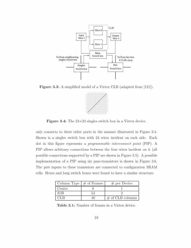
only connects to three other ports in the manner illustrated in Figure 3.4.
Shown is a singles switch box with 24 wires incident on each side. Each
dot in this figure represents a programmable interconnect point (PIP). A
PIP allows arbitrary connections between the four wires incident on it (all
possible connections supported by a PIP are shown in Figure 3.5). A possible
implementation of a PIP using six pass-transistors is shown in Figure 3.6.
The gate inputs to these transistors are connected to configuration SRAM
cells. Hexes and long switch boxes were found to have a similar structure.
Column Type # of Frames # per Device
Center 8 1IOB 54 2CLB 48 # of CLB columns
Table 3.1: Number of frames in a Virtex device.
24

Figure 3.5: All possible connection of a subset switch.
Figure 3.6: A six pass-transistor implementation of a switch point.
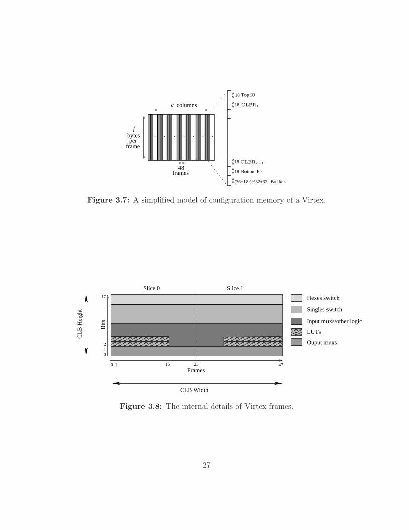
The configuration memory of a Virtex device is organised into so-called
frames [129]. A frame is the smallest unit of configuration data. A frame
register spans the entire height of the device and configures a portion of a
column of Virtex resources (Figure 3.7). There are three types of frames
excluding BRAM frames (Table 3.1). The centre type frames configure the
clock resources. The IO type frames configure the left and right IO blocks.
The number of these frames is fixed for the variety of device sizes within the
family. The CLB type frames form the bulk of the configuration data. These
frames configure a column of CLBs and the corresponding top and bottom
IO blocks. There are 48 CLB frames per column of CLBs. The structure of a
frame is also shown in Figure 3.7. A frame contributes 18 bits of SRAM data
to the top IO block, 18 bits to the bottom IO block and 18 bits per CLB that
it spans. Thus the frame size is 36+18r where r is the number of rows in the
device. The frame is padded with zeros to make it an integral multiple of 32
followed by an extra 32-bit pad word (e.g. an XCV1000, which has 64 rows
25

of CLBs, has a frame size of 1,248 bits). The configuration port is 8-bits wide
and can be clocked at 66MHz. Virtex supports DMA-like addressing at the
frame level. The user supplies the starting frame address and the number of
consecutive frames to load followed by the frame data. A configuration can
contain one or more contiguous blocks of frames.
The Virtex datasheet does not provide much detail about the internal
structure of a frame other than the features summarised above. However, by
examining the JBits API and through trial and error, a rough sketch of the
internal structure of a frame has been determined (Figure 3.8). Shown is an
18× 48 block of bits that corresponds to a CLB worth of configuration. The
configuration memory was found to be quite symmetrical with respect to the
two slices. As can be seen, each frame controls the setting of a portion of the
switch, connection and logic configuration SRAM within a CLB.
The Virtex-4 LX FPGAs, introduced in 2004, offer much greater func-
tional density than the Virtex devices [124]. As in the Virtex-II architecture,
each CLB in the new device contains four slices where each slice has a similar
structure as in a Virtex. The largest in the family (an XC4VLX200) is organ-
ised as an array of 192×116 CLBs. The smallest unit of configuration is still
called a frame. However, the frame size is fixed at 164 bytes for all device
sizes ( there are 40,108 frames in an XC4VLX200) and controls a portion
of the configuration memory for 16 vertically aligned CLBs. The 8-bit wide
configuration port is clocked at 100MHz.
3.2.2 The system model
In order to build a complete system, an FPGA needs to be integrated with
other subsystems that perform functions such as device (re)configuration and
data streaming. This results in a system called a reconfigurable computer.
This section classifies these computers based on the level of integration be-
tween an FPGA and the other components of the system.
26
c
fbytes
48frames
perframe
columns
18
18
18
18
(36+18r)%32+32
Top IO
Pad bits
Bottom IO
CLBR1
CLBRr−1
Figure 3.7: A simplified model of configuration memory of a Virtex.
0 1 23 4715
012
Slice 1
Singles switch
LUTs
Input muxs/other logic
Ouput muxs
Hexes switch17
Slice 0
Frames
CLB Width
CL
B H
eigh
t
Bits
Figure 3.8: The internal details of Virtex frames.
27

Board-level integration
Most commonly, an FPGA is fabricated on a single chip and is integrated with
supporting circuitry on a PCB. In embedded systems, the support circuits
include flash memories to store configuration data, configuration controllers
and IO interfacing logic. The configuration data is loaded onto the device at
system boot-up time. The FPGA’s configuration remains static during the
system operation. The configuration ROM is only modified when the entire
system needs to be upgraded.
Increasingly, FPGAs are seen as general purpose accelerators for a wide
variety of applications such as digital imaging, encryption and, network pro-
cessing. It is therefore important to integrate an FPGA chip with a general
purpose system that offers flexible configuration and IO control. A common
solution is to mount the device on a PCB which is then directly attached
to the system bus of a controlling processor. The configuration and IO can
be performed under the control of the host microprocessor via a command
line interface or through a programming interface. This type of integration
is often referred to as loose coupling. An example of such as system is given
below.
Example: The Celoxica RC1000 board
A simplified block diagram of the Celoxica RC1000 board is shown in
Figure 3.9. It contains a Virtex device, four SRAM banks, auxiliary IO
and the PCI compatible interfacing logic [107]. The secondary PCI bus is
32-bit wide and runs at 33MHz. The IO chip has a local bus that also
operates at 33MHz. The registers of this chip can only be accessed by the
host microprocessor which can setup DMA transfers in either direction. The
IO chip is also used for configuration control, FPGA clocking and FPGA
arbitration. The on-board memory banks are of size 512K×32 bits each and
can be accessed by the FPGA in parallel. These banks are accessed by the
host processor via the attached PCI bus. Proper device drivers must be
installed on the host operating system in order to access the board from a
28

IOPeripheral
Secondary PCI bus
SRAM
SRAM
SRAM
SRAM
Bus master
BridgePCI−PCI
Primary PCIHost
Clock &Control
VirtexXCV1000
512K×32
512K×32
512K×32
512K×32
Figure 3.9: The Celoxica RC1000 FPGA board.
user application [108].
Chip-level integration
The ever increasing transistor density has resulted in novel systems-on-chip
(SoC) in which a microprocessor is fabricated along with a programmable
gate arrays on a single die. The benefit of this approach is that the chip can
now be installed as a stand-alone system and the internal processor can be
used for FPGA configuration control and IO.
Example: Virtex-II Pro & Virtex-4 FX
The Virtex-II Pro family enhances the Virtex model by increasing the
functionality of its CLBs and by introducing up to two PowerPC RISC pro-
cessors on a single chip [126]. Each CLB in a Virtex-II Pro device contains
four slices where each slice has a similar structure as in a Virtex device. The
largest device in the family (XC2VP100) is organised as an array of 120×94
CLBs and contains two IBM PowerPCs. Each PowerPC is pipelined having
29

five stages, running at 300MHz and containing data and instruction caches
each of size 16KB.
The unit of configuration in a Virtex-II Pro is also called a frame. The
structure of a frame is not clear from the data sheet. However, the frame
size is significantly larger than that of a Virtex. There are 3,500 frames in a
complete configuration of an XC2VP100. Each frame contains 1,224 bytes.
The configuration port is 8-bits wide and can be clocked at 50MHz.
The Virtex-4 FX devices further enhance the functional density of Virtex-
II devices with the CLB structure being almost the same. The largest in the
family, an XC4VFX140, is organised as an array of 192×84 CLBs. It also
contains a five-stage IBM Power PC running at 450MHz. The processor has
data and instruction caches each of size 16KB. Each Virtex-4 FX device has
a fixed frame size of 164 bytes (an XC4VFX140 needs 41,152 frames for a
complete configuration). The configuration port is 8-bit wide and can be
clocked at 100MHz.
Tightly coupled systems
Researchers have been investigating so-called tightly-coupled systems where
programmable gate arrays are directly integrated within a processor’s data-
path. An example of such a system is the Chimaera processor.
Example: Chimaera processor
The programmable gate arrays in Chimaera is tightly coupled with the
host processor on a single die. The gate array can directly access the pro-
cessor’s data registers via a shadow register file [36]. These shadow registers
contain the same data as the main registers. The gate array is organised as
a two-dimensional grid of r× c basic blocks (BBs) (32×32 in the prototype).
The logic block in a BB can be configured as a 4-LUT, two 3-LUTs or one
3-LUT with a carry. The gate array provides a mesh-like interconnect struc-
ture. Each BB can be directly connected to its four neighbours. Each row
of BBs also contains a long wire to support global connections.
30

The gate array in Chimaera is runtime partially reconfigurable with a row
being the smallest unit of configuration and needing 208 bytes of configura-
tion data. Reconfiguration is performed on a row by row basis during which
the processor is stalled. Several rows can be configured in sequence without
needing their individual addresses (as done frame-wise in Virtex). Special
reconfiguration instructions are added to the processor ISA. These instruc-
tions contain the necessary control information for loading the configurations
from memory. The configuration port width and the clock speed were not
reported in [36].
3.3 Programming Environments
3.3.1 Hardware description languages
FPGAs have their origin in the electronic design automation industry. The
programming tools therefore reflect this at all levels of abstraction. In this
context, hardware description languages (HDLs), such as VHDL and Verilog,
have served their purposes quite well and industry standard design environ-
ments exist to support these languages (e.g. [120, 109, 116]).
A typical design flow is shown in Figure 3.10. The input design is specified
using an HDL (or graphical design tool such as schematics). This specifica-
tion is transformed into an internal representation and is then simulated (for
example using ModelSim [115]). This step is necessary to ensure that the
specified system behaves in the manner intended. After this functional veri-
fication, the input design is synthesised. The purpose of this logic synthesis
is to construct an area/time efficient abstract representation of the input cir-
cuit. The result is a netlist which is essentially a list of functional blocks (such
as gates) and their interconnection. This netlist is then technology-mapped
onto the target logic block architecture. This step packs the functional logic
into the target logic block in an area efficient manner. The technology-
mapped netlist is then placed and routed onto the target FPGA and a con-
31

figuration file that contains the actual data to be transferred onto the device
is finally generated. An optional timing may be performed to verify that
timing constraints are met and to prompt re-implementation of the design
if not. Once a configuration file has been generated by the vendor-supplied
CAD tool, it can be loaded onto the FPGA or it can be stored in a flash
memory in case the FPGA is to be deployed in an embedded environment.
The extension of the above design flow for runtime reconfigurable applica-
tions is elaborated using a hypothetical scenario. Suppose that a particular
application is to be implemented on an FPGA of a certain size. The designer
has partitioned the application into four modules A to D, as shown in Figure
3.11, and has developed an HDL description for each component separately.
During placement and routing step, it is found that the target FPGA is
not large enough to accommodate all four components simultaneously and
only one component can be implemented at any point in time. Thus, the
designer decides to use dynamic reconfiguration to emulate a larger FPGA.
Each module is placed and routed independently and configuration data for
each is generated. At runtime, each module is configured in turn and an
external program receives the output of the currently configured circuit and
feeds it to the module configured next and so on. It is fair to claim that such
an application can be developed using commercial tools such as Xilinx ISE
[120].
Next, suppose a different application with four modules, A, B, C and D.
Figure 3.12 shows the manner in which these modules are to be combined to
form a reconfigurable application. In this graph, each node corresponds to a
configuration state of the target FPGA while edges represent reconfiguration.
Assume that the device starts in its default configuration state. After its first
configuration, modules A and B are supposed to be on-chip with the user
data input to module A, which performs some computation on them and
outputs to module B. The output of the module B is taken to be the output
of this step. The FPGA is then reconfigured and the modules A, C and D
are to be loaded onto the device with data flowing from A to C to D. It is
32

Specification(HDL/schematics)
Simulation
Logic Synthesis
Technology Mapping
Place&Route
Generateconfiguration
file
Configurationfile
Figure 3.10: Typical FPGA design flow.
33
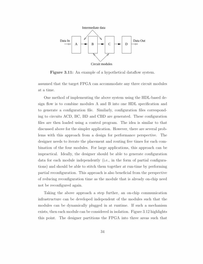
A B C DData In Data Out
Intermediate data
Circuit modules
Figure 3.11: An example of a hypothetical dataflow system.
assumed that the target FPGA can accommodate any three circuit modules
at a time.
One method of implementing the above system using the HDL-based de-
sign flow is to combine modules A and B into one HDL specification and
to generate a configuration file. Similarly, configuration files correspond-
ing to circuits ACD, BC, BD and CBD are generated. These configuration
files are then loaded using a control program. The idea is similar to that
discussed above for the simpler application. However, there are several prob-
lems with this approach from a design for performance perspective. The
designer needs to iterate the placement and routing five times for each com-
bination of the four modules. For large applications, this approach can be
impractical. Ideally, the designer should be able to generate configuration
data for each module independently (i.e., in the form of partial configura-
tions) and should be able to stitch them together at run-time by performing
partial reconfiguration. This approach is also beneficial from the perspective
of reducing reconfiguration time as the module that is already on-chip need
not be reconfigured again.
Taking the above approach a step further, an on-chip communication
infrastructure can be developed independent of the modules such that the
modules can be dynamically plugged in at runtime. If such a mechanism
exists, then each module can be considered in isolation. Figure 3.12 highlights
this point. The designer partitions the FPGA into three areas such that
34

Null
AB
ACD
A B FPGA
CommunicationInter−Circuit
A C D
Reconfiguration
BD
CBD
BC
Figure 3.12: An example reconfigurable system. The circuit schedule isshown on the left while various configuration states of the FPGA on theright.
each partition can accommodate any of the modules discussed above. A
communication infrastructure is placed that allows arbitrary communication
between the on-chip modules. What remains is to decide where to place each
module at runtime.
Consider the reconfiguration from the state ACD to BC. There are two
possible placements of the modules. Firstly, the designer can configure mod-
ule B on top of module C and module C on top of module D. However, since
the communication infrastructure allows arbitrary communication between
the modules, the designer can simply configure module B on top of module
D thereby reducing the reconfiguration time. Now consider the transition
ACD→BD. Using the same reasoning, module B can overwrite either mod-
ule C or module A. However, we note that module C will be needed if the
system makes the transition BD→CBD. Thus, it is more useful to configure
B over A. Configuration caching techniques essentially perform this type of
scheduling to reduce the overall reconfiguration delay of an application. A
35

basic assumption made by these methods is that the reconfigurable modules
are re-locatable.
The problem of reducing the overall reconfiguration time of the above ap-
plication can be considered at a different level. Consider the above scenario.
When the device is reconfigured from state AB to state ACD, either module
C or module D must replace module B. The module designer can implement
modules C and B such that a significant number of sub-modules between
them are common. Thus, the cost of reconfiguring C over B is much less than
the cost of reconfiguring D over B. This approach, however, requires that the
sub-modules that are common between C and B are physically located at
the same place in both modules and the configuration data corresponding to
these sub-modules is identical. These conditions are difficult to meet with
current CAD tools. Even if one could implement this scheme, there is a
further assumption that partial reconfiguration can be applied at the level
of granularity demanded by the two sub-modules. Virtex devices, for exam-
ple, offer a frame-oriented reconfiguration and thus any implementation of
the common sub-modules is constrained by this limitation. Another method
of reducing reconfiguration time is to examine the configuration files corre-
sponding to modules B, C and D to identify opportunities for compressing
them. These issues will be discussed in more detail in Section 3.5.
There exists some support in commercial CAD tools for developing recon-
figurable applications as outlined above. The operating system view extends
the above ideas into a more generic framework (e.g. [8, 7, 67, 87, 84]). A
large number of researchers have proposed solutions to such problems as cir-
cuit placement and scheduling (e.g. [9, 28, 27, 1, 17]), reconfigurable module
design, inter-module communication, and data management. Several pro-
totypes operating systems for reconfigurable computers have been designed
and built (e.g. [96, 111, 6]).
The term module, in the above general context of an operating system,
has several other names such as a swappable logic unit [8], a hardware task
[96], a circuit core [76, 59], and a dynamic hardware plugin [91]. Each of these
36

terms is applied at a different level of abstraction and essentially means a
single circuit entity that is reconfigured onto the device. This thesis uses
the term core because the benchmark circuits that have been collected from
various sources use this term to mean a single application, described in a
high-level language, that can be implemented on an FPGA. An example of
a core will be given in Section 3.4.
3.3.2 Conventional programming languages
Several researchers have advocated the use of conventional programming lan-
guages, such as C/C++/Java, for runtime reconfigurable FPGAs. Several
extensions to such languages have been proposed (e.g. [34, 3, 106]). The
main argument in favour of these language systems is that the vast majority
of system developers is more familiar with these paradigms than with HDLs.
An example programming system for Virtex devices is the JBits class
library [121]. The JBits class library is a Java API that can be regarded
as an interface to the underlying configuration data and a high-level envi-
ronment for reconfiguration control. Please note that this is different from
conventional HDL flows that hides all architectural details from the program-
mer. Given an enhanced view of the underlying hardware, reconfiguration
can be performed at a finer level to customise the circuits at runtime. This
capability has been used to achieve two different purposes:
1. Instead of implementing a general purpose circuit, a specialised cir-
cuit is implemented. For example, rather than implementing a general
purpose adder, one can implement an adder that adds an input num-
ber with a constant. When this constant changes, the adder circuit
can be reconfigured to adapt to new requirements. The benefit of this
approach is that a specialised circuit tends to be smaller and faster
then its general purpose counterpart. Reconfiguration is performed to
meet the changing needs of the computation. An example application
is presented in Section 3.4.
37

2. As specialised circuits tend to be smaller, this technique can be used
to overcome resource limitations when a general purpose circuit cannot
fit onto a given sized FPGA.
In both cases, the user generates new partial configuration data at run-
time, depending on the inputs at hand, and loads them onto the chip. This
raises new challenges in the design of reconfigurable applications. Given that
placement and routing are time consuming tasks, in general, they cannot be
performed at runtime as the time saved from implementing a smaller circuit
is outweighed by the time used in actually placing and routing the circuit.
While some high-level (e.g. [10]) and some low level solutions (e.g. [45]) have
been proposed to solve this problem, the usual approach is not to perform
placement and routing at runtime and only update LUTs (as in the CirCal
interpreter, which is discussed in Section 3.4). This method demands that
the FPGA vendor has provided an API that allows the designer to directly
modify configuration data in various LUTs. The JBits 2.8 library does pro-
vide such an interface for Virtex devices but there is no update on JBits to
support the recent FPGAs. Thus, circuit specialisation is difficult to achieve
on the current devices.
3.4 Examples of Runtime Reconfigurable
Applications
This section discusses common uses of runtime reconfiguration with exam-
ples from the literature. It is shown that while runtime reconfiguration is
beneficial in many cases, reconfiguration time in contemporary devices limits
the maximum performance benefit.
38

3.4.1 A triple DES core
The following example shows that a Virtex-II implementation of a DES core
can significantly outperform a Pentium-IV implementation in terms of speed.
However, if time to configure the circuit onto the device is also taken into
account then the performance improvement is marginal.
The Triple-DES algorithm was implemented on an SRC-6E board [31].
An SRC-6E board consists of two double-processor boards and one Multi-
Adaptive Processor (MAP) containing four Virtex-II XC2V6000 devices. The
time taken to configure the DES core, to transfer data to the FPGA and to
perform encryption was measured for various input data sizes (Figure 3.13.a).
It can be seen that the time needed to transfer data to the FPGA and to
process it is significantly less than the time needed to actually configure the
circuit.
The above results were compared with a Pentium-IV (1.8GHz, 512KB
cache and 1GB main memory) implementations of the same algorithm. Two
implementations were considered. The first was a C description of the al-
gorithm while the second was more optimised by having a mix of C and
assembly. The results are shown in Figure 3.13.b. It can be seen that if
the configuration overheads are removed (MAP without configuration) then
a significant performance improvement can be observed compared with a
Pentium-IV.
3.4.2 A specialised DES circuit
Rather than implementing a general purpose DES circuit capable of accepting
all keys, one can customise the circuit around the current key. Similarly, if
only encryption is to be performed then no decryption circuitry need to be
configured.
The DES core can be parametrised based on the input key and mode
(encrypt or decrypt). A performance comparison between a general purpose
39

(a) Components of DES execution time on MAP
(b) Performance comparison with a Pentium-IV
Figure 3.13: Performance measurements for Triple DES [31].
40

DES and specialised DES on an XCV300 was reported in [24]. The cores were
sepecified and compiled using the Pebble design environment [55]. Pebble
stands for Parametrised Block Language and the the former paper examines
the runtime parametrisation of the DES cores within this framework.
The paper [24] considered three designs (Table 3.2). The static design was
the general purpose circuit capable of changing key or mode within a cycle.
The design labelled bitstream produced configuration data for all possible key
and mode combinations (i.e there was a configuration for each key, mode set).
Thus, at runtime only one configuration needed to be selected and loaded
based on the current key and mode. It should be noted that the specialised
design consumed less than half the chip area of the general, static design.
The time needed to change the circuit in this particular case was limited by
the time needed to load the configuration onto the device. This approach
was found to be impractical as there are more than 107 different key/mode
combinations in DES.
The final approach was to generate only one configuration and load it
onto the chip initially. At runtime, based on the current key and mode, this
configuration was updated using JBits [121]. This software was run on a
Pentium-III (500MHz) with Sun JDK1.2.2. There were two delays involved:
time to generate updated configuration data and time to load it onto the
device. Figure 3.14 shows the average processing time needed to change the
key and process the data. The curve labelled RTPebble corresponds to a de-
sign compiled within the Pebble design framework whereas the design JBits
was a hand-optimised version. As can be seen, reconfiguration takes quite
a significant portion of the time observable in the figure as a reduction in
processing rate, unless the amount of data to be processed is quite large (i.e.
the execution time is many orders of magnitude large than the reconfigura-
tion time, or to put it another way, when reconfiguration frequency is low
compared to the execution delay). Thus, performance improvements can be
gained if reconfiguration overheads are reduced.
41

Design Speed Reconfig. Time Area BitstreamGbits/s ms CLB KB
Static 10.1 - 1,600 220Bitstream 10.7 1.5x 770 91xJBits 10.7 92 770 91
Table 3.2: Performance comparison of a general purpose vs. specialisedDES. x denotes the number of configurations generated [24].
Figure 3.14: Performance measurements for Triple DES [24].
42

3.4.3 The Circal interpreter
Another method where circuit updates are useful is when an entire circuit
does not fit within available FPGA resources, or resource requirements are
not known apriori. In this case, a base circuit is initially implemented and is
updated at runtime as required. Given that routing is one of the most time
consuming processes during circuit mapping, a common approach is to place a
wiring harness [8] during circuit initialisation and update only logic resources
at runtime. This form of hardware virtualisation is different from algorithm
partitioning discussed earlier. The difference is that in the previous case, data
output from a sub-core needs to be input to the next configured sub-core.
Moreover, the two successive sub-cores might have nothing in common. In
the present case, there is really only one circuit that is updated as required.
An example of such as system is the Circal Interpreter discussed in this
section.
As mentioned in Section 1.2, Circuit Calculus (Circal) is a process alge-
braic language that has been proposed as a suitable high-level language for
specifying runtime reconfigurable systems [69]. It extends conventional finite-
state machine models by introducing structural and behavioural operators.
Structural operators allow the decomposition of a system in a hierarchical
and modular fashion down to a desired level of specification. Behavioural
operators allow the user to model the finite-state behaviour of the system
where state changes are conditioned on occurrences of actions drawn from a
set of events.
Circal processes can be looked upon as interacting finite-state machines
where events occur and processes change their states according to their def-
initions. These processes can be composed to form larger systems with con-
straints on the synchronisation of event occurrence and process evolution.
Given a set of events, all composed processes must be in a state to accept
this set before any one of them can evolve. If all agree on accepting this set,
they all simultaneously evolve to the prescribed next state.
43

A Circal compiler for generating an implementation of a specified system
of processes was developed on an XC6200 [30]. This system was limited
in the sense that as Circal specifications grew in size, they could not be
mapped onto the limited resources offered by an XC6200. An interpreter
targeting much larger Virtex devices was subsequently developed [29, 63].
The interpreter translates a Circal specification given as a state-transition
graph and implements as much of system as is possible at any point in time.
During initialisation, the interpreter partitions the chip area into strips and
allocates a pre-sized block to each process depending on its anticipated needs.
In addition to this, enough area is allocated to a process so as to satisfy its
minimum resource demands at any point during its execution. The wiring
between the sub-modules of each process remains fixed and is configured
during initialisation. Only LUT updates are performed at runtime.
At runtime, the interpreter selects a subgraph of each process, where the
size of the subgraph depends on the area allocated to that process. The
selected subgraph is then transformed into bitstreams using JBits. These
correspond to the circuit updates needed at that point in time. As processes
evolve, different portions of their state-graphs are selected and implemented.
In this manner large specifications can be interpreted, thus automatically
overcoming hardware limitations. Care was taken in the physical layout of
each process in order to take advantage of column-oriented reconfiguration
in Virtex devices.
The performance of the interpreter was measured. Only one process was
implemented while its size was varied. The resulting circuit occupied one
or more columns of an XCV1000. Results are shown in Figures 3.15, 3.16
and 3.17. The initialisation time refers to the time taken to generate the
bitstream from the initial Circal subgraph. The circuit update specification
time refers to the time take to generate an updated bitstream from a new
subgraph of the same process. The partial reconfiguration time is the time
needed to load or partially reconfigure the FPGA.
It can been seen that the initial bitstream generation is significantly longer
44

0
5
10
15
20
25
30
15 20 25 30 35 40 45 50
Circ
uit I
nitia
lisat
ion
Tim
e (s
econ
ds)
FPGA Circuit Width (CLBs)
Figure 3.15: Circuit initialisation time of the CirCal interpreter [63].
0
20
40
60
80
100
120
140
160
15 20 25 30 35 40 45 50
Circ
uit U
pdat
e S
peci
ficat
ion
Tim
e (m
illis
ecs)
FPGA Circuit Width (CLBs)
Figure 3.16: Circuit update time of the CirCal interpreter [63].
45

0
1
2
3
4
5
6
7
8
15 20 25 30 35 40 45 50
Syn
chro
nisa
tion
and
Par
tial R
econ
figur
atio
n T
ime
(mill
isec
s)
FPGA Circuit Width (CLBs)
Figure 3.17: Partial reconfiguration time of the CirCal interpreter [63].
than the update bitstream generation. This is mainly due to the router run-
time at initialisation. Circuit update times are in sub-second domain for
the circuit sizes tested. The main bottleneck of programming configuration
bitstreams lies in performing bit-oriented manipulations of the large configu-
ration bitstreams in JBits that operates under a Java virtual machine model
of computation. Assuming these configurations have been generated apriori,
the time needed to load configuration also puts a limit on how quickly a
Circal system can respond to external inputs.
3.5 Problem Formulation
3.5.1 Motivation
The previous section presented various examples of runtime reconfigurable
applications and showed that they have a potential to outperform conven-
46
tional system implementations. In many cases, runtime reconfiguration must
be used because the system to be implemented cannot fit on the available
FPGA resources or their resource requirements are not known during ini-
tialisation. In these cases, reconfiguration time represents an overhead that
must be reduced.
This thesis focuses on reducing the time needed to reconfigure an FPGA.
As was discussed in Section 3.3, this problem can be addressed at several
levels such as at the configuration data level, at the placement/scheduling
level or even at a design level. The problem must be addressed at all these
levels for a complete solution. However, given the complexity of the issues,
not all levels can be examined in one project. The present work focuses only
on the configuration data level as this represents the lowest level upon which
the other levels depend. A thorough understanding of the problem at this
level is needed before work at the other levels can be advanced.
As was discussed in the previous section, an FPGA can be reconfigured to
achieve several different purposes, such as to overcome resource limitations,
or to implement circuits that are customised around certain data inputs.
The OS concepts essentially extend these ideas by providing convenient APIs.
The present work focuses on core style reconfiguration in which various circuit
cores are swapped in and out of the device. It is assumed that the circuit
placement and scheduling has already been done. Lastly, to further simplify
the problem, no space sharing between the cores or caching of the cores is
allowed. In other words, only one circuit core can be active at any time and
it is assumed to be entirely replaced by the following core.
Applications, such as circuit customisation, might not fit into the above
picture. However, the author believes that such applications are limited in
number. As devices become more complex, it will become difficult to hand-
map applications to exploit the benefits of small circuit updates. While
some work has been done towards automating this operation in the context
of XC6200 devices (e.g. [56]), the author is not aware of any similar work
that targets contemporary devices. Moreover, it might not be possible for
47

end users to hand-map their applications as the device manufacturers do not
provide the necessary details on the FPGA architecture and the bitstream
format, knowledge that is necessary for any circuit mapping procedure. The
abstraction of a circuit core, on the other hand, is widely applicable and
thus our problem statement in the next section implicitly assumes that each
circuit in an input sequence of configurations corresponds to a circuit core.
3.5.2 Problem statement
The input is a sequence of configurations, C1, C2....Cn, that must be loaded
onto the device in the given order. The problem can be stated as following:
Minimizen∑
i=1
(Ri,i+1) (3.1)
Here Ri,i+1 is the reconfiguration time from configuration i to i + 1.
48

Chapter 4
An Analysis of Partial
Reconfiguration in Virtex
4.1 Introduction
The focus of this chapter is on the use of partial reconfiguration as a method
for reducing reconfiguration time on a reconfigurable computer. Partial re-
configuration alters the configuration state of a subset of the available config-
urable elements in an FPGA. More concretely, instead of loading configura-
tion data for each and every element, the user loads new data only for those
elements whose configuration state is to be changed. This has the potential
to allow faster reconfiguration as less data needs to be transferred into the
configuration memory of the machine.
While it is clear that partial reconfiguration has advantages over complete
reconfiguration, it is less clear to what extent one can rely on this method as
a general technique for reducing reconfiguration time. It is also not clear how
device-specific configuration memories impact upon the performance of par-
tial reconfiguration and what parameters of user circuits and of CAD tools
are important in this context. This chapter examines these questions by em-
pirically studying the use of partial reconfiguration in a commercial device,
49

Virtex. It is shown that the large configuration unit size of these devices
forces the user to load a significant amount of redundant data in a typical
circuit configuration. Methods to support fine-grained partial reconfigura-
tion are presented. The next chapter presents new configuration memory
architectures that support these new methods.
This section first presents the experimental environment that was setup
for the purpose of analysing partial reconfiguration (Section 4.1.1). The
analysis presented in this chapter is based on empirical methods. A set of
benchmark circuits was mapped onto a commercially available FPGA and
their configuration data analysed in detail. Section 4.1.2 presents the method
by which various parameters of the device, of the associated CAD tools and
of the circuits were identified as being relevant. This section presents a high-
level view of the experiments and analysis presented in detail later in this
chapter.
4.1.1 The experimental environment
The experimental environment consisted of several hardware and software
components. An RC1000 board [107] containing an XCV1000 device was
used as a plug-in for a Pentium-IV machine (2.6GHz, 256M RAM). On the
software side, Xilinx ISE CAD version 5.2 [120] tools were used for mapping
the benchmark circuits. The JBits 2.8 package [121] was used for config-
uration processing. A number of Java/C++ programs were developed for
various experiments detailed later in this chapter.
The FPGA family considered in this work was Virtex. There were sev-
eral reasons for targeting this device. Firstly, this device is commonly used
in industry and academia alike. Several important findings in the area of
configuration compression have targeted Virtex devices (as was discussed in
Chapter 2). Secondly, Virtex provides a low-level programming interface
to its bitstream (JBits 2.8). This API facilitates manipulation of Virtex
configuration data. Lastly, Virtex devices and associated CAD tools were
50
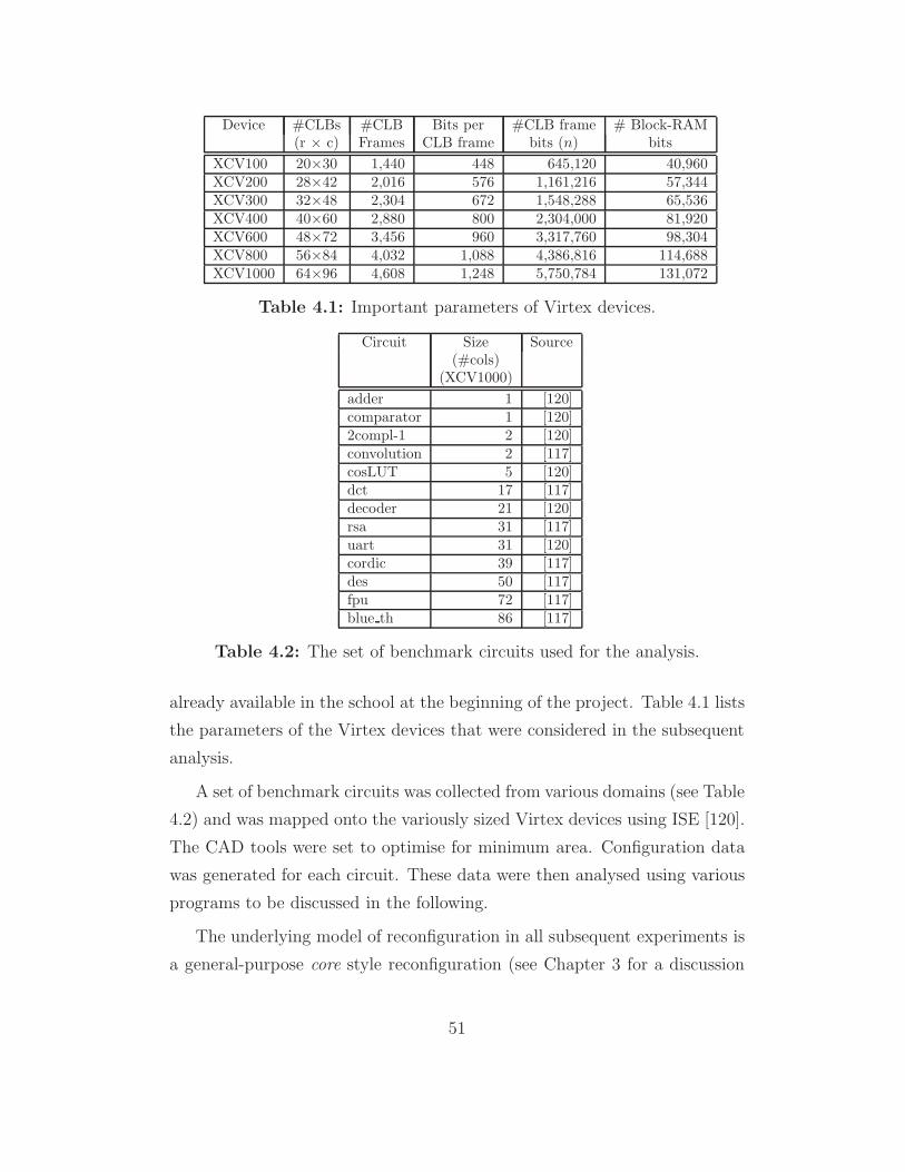
Device #CLBs #CLB Bits per #CLB frame # Block-RAM(r × c) Frames CLB frame bits (n) bits
XCV100 20×30 1,440 448 645,120 40,960XCV200 28×42 2,016 576 1,161,216 57,344XCV300 32×48 2,304 672 1,548,288 65,536XCV400 40×60 2,880 800 2,304,000 81,920XCV600 48×72 3,456 960 3,317,760 98,304XCV800 56×84 4,032 1,088 4,386,816 114,688XCV1000 64×96 4,608 1,248 5,750,784 131,072
Table 4.1: Important parameters of Virtex devices.
Circuit Size Source(#cols)
(XCV1000)adder 1 [120]comparator 1 [120]2compl-1 2 [120]convolution 2 [117]cosLUT 5 [120]dct 17 [117]decoder 21 [120]rsa 31 [117]uart 31 [120]cordic 39 [117]des 50 [117]fpu 72 [117]blue th 86 [117]
Table 4.2: The set of benchmark circuits used for the analysis.
already available in the school at the beginning of the project. Table 4.1 lists
the parameters of the Virtex devices that were considered in the subsequent
analysis.
A set of benchmark circuits was collected from various domains (see Table
4.2) and was mapped onto the variously sized Virtex devices using ISE [120].
The CAD tools were set to optimise for minimum area. Configuration data
was generated for each circuit. These data were then analysed using various
programs to be discussed in the following.
The underlying model of reconfiguration in all subsequent experiments is
a general-purpose core style reconfiguration (see Chapter 3 for a discussion
51

of the concept of a core). It is assumed that the target Virtex device is
time-shared between various unrelated applications (see Figure 4.1). Each
circuit core in the benchmark corresponds to one application. These cores
are switched in and out of the device according to a fixed sequence. In
other words, we are given a sequence of configurations corresponding to the
benchmark circuit cores. These configurations must be loaded in the same
sequence as they are input. The goal is to reduce the total time needed to
reconfigure the entire sequence.
FPGACurrent state
FPGANext stateCore
Next
Figure 4.1: An example core-style reconfiguration when the FPGA is timeshared between circuit cores.
4.1.2 An overview of the experiments
The partial reconfiguration problem is complex as it involves not only the user
circuits but also the CAD tools and the target devices. A research framework
was therefore established to systematically approach this problem (Figure
4.2). The author followed an iterative experimental procedure initiated by
measuring the amount of data required to configure a sequence of real circuits
on a commercially available partially reconfigurable FPGA. The circuits were
mapped using the vendor-supplied CAD tools. New models of CAD tools and
of FPGAs were developed as a result of the observed poor performance. The
performance of these hypothetical systems was then measured using the same
configuration data set. The respective parameters of the problem were thus
identified and analysed using an iterative modelling procedure. This section
provides a high-level view of this research method and contains pointers to
various sections that provide the details.
52
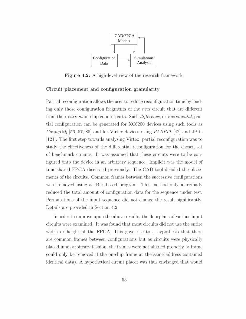
Simulations/Analysis
Configuration Data
CAD/FPGAModels
Figure 4.2: A high-level view of the research framework.
Circuit placement and configuration granularity
Partial reconfiguration allows the user to reduce reconfiguration time by load-
ing only those configuration fragments of the next circuit that are different
from their current on-chip counterparts. Such difference, or incremental, par-
tial configuration can be generated for XC6200 devices using such tools as
ConfigDiff [56, 57, 85] and for Virtex devices using PARBIT [42] and JBits
[121]. The first step towards analysing Virtex’ partial reconfiguration was to
study the effectiveness of the differential reconfiguration for the chosen set
of benchmark circuits. It was assumed that these circuits were to be con-
figured onto the device in an arbitrary sequence. Implicit was the model of
time-shared FPGA discussed previously. The CAD tool decided the place-
ments of the circuits. Common frames between the successive configurations
were removed using a JBits-based program. This method only marginally
reduced the total amount of configuration data for the sequence under test.
Permutations of the input sequence did not change the result significantly.
Details are provided in Section 4.2.
In order to improve upon the above results, the floorplans of various input
circuits were examined. It was found that most circuits did not use the entire
width or height of the FPGA. This gave rise to a hypothesis that there
are common frames between configurations but as circuits were physically
placed in an arbitrary fashion, the frames were not aligned properly (a frame
could only be removed if the on-chip frame at the same address contained
identical data). A hypothetical circuit placer was thus envisaged that would
53

place each circuit in the input sequence such that the number of common
frames between its configuration and the previous circuit’s configuration was
maximised. This line of thinking was motivated by a result reported in [46]
that more than 80% of bits between typical Virtex cores are common.
As running placement and route tools take time, and there is potentially
a large number of possible physical placements for each circuit, a method for
quickly analysing the impact of circuit placement on partial reconfiguration
had to be developed. This problem was tackled at the configuration data level
by considering a hypothetical Virtex device. If we assume the Virtex device
is homogeneous, i.e. one can simply cut and paste a mapped circuit anywhere
on the device without needing to re-place and re-route, then variable circuit
placement could be simulated by assuming various physical placements of
the input partial configurations.
As a first step, a one-dimensional partial reconfiguration problem was
considered where circuits are restricted to move horizontally. The objective
was to find the best placement of each partial configuration relative to the
others in the input sequence such that the total amount of configuration
data was minimised. A greedy heuristic was investigated which resulted
in marginal reductions in the total amount of configuration data produced
by the sequence. It was found that it was not the greedy algorithm that
performed poorly, but rather that common frames in the input configurations
were located such that no placement would result in significant improvements.
Details of this analysis are provided in Section 4.3.
The result of the above experiment suggested another hypothesis. As
the unit of configuration in Virtex is quite large, it forces the CAD tool to
include a frame even if it differs from the target frame by a single bit. A
hypothetical Virtex was considered that allows sub-frames of various sizes to
be loaded independently in a manner similar to conventional SRAMs. As the
sub-frame size was reduced, dramatic reduction in required frame data was
observed for the sequence of configurations considered previously. In general,
a smaller configuration granularity allowed more data to be removed from
54
the sequence. However, at this level, the increased overhead of addressing
configuration units outweighed any reduction achieved for the frame data.
This consideration led to a model Virtex that balanced the addressing over-
head by keeping the configuration unit slightly larger. This Virtex required
one third less configuration data on average, compared with when the current
Virtex for the same sequence of input configurations. Details are provided in
Section 4.4. The results of Sections 4.2, 4.3 and 4.4 were published in [60].
Explaining inter-configuration redundancy
In order to explain the above results, two sources of inter-configuration re-
dundancy were identified. A configuration fragment controlling a particular
subset of the device resources can be removed between two successive con-
figurations if:
• The next circuit uses the same resource and requires it to be in the
same configuration state, or
• Neither of the circuits uses that resource and the CAD tool assigns it
a default configuration state.
It was experimentally determined that the second case is responsible for
the majority of inter-configuration redundancy. This was confirmed by re-
moving all default-state, or null, configuration data from the input configu-
rations and then finding inter-configuration differences as before. Details are
provided in Section 4.5.
The default-state reconfiguration
The above experiments suggested that a typical circuit makes a small number
of changes to the default configuration state of the device. This is what
can be referred to as default-state reconfiguration. Further experiments were
performed to gauge the impact of increasing or decreasing the FPGA size
55
on the amount of reconfiguration data required for a typical default-state
reconfiguration. The available circuits were mapped onto variously sized
Virtex devices. The amount of null data in each configuration was then
removed at the bit level. It was found that the number of essential frame
bits for a circuit configuration increased just slightly with device size. Details
are provided in Section 4.6.
The picture that emerged out of the above analysis suggested that it might
be useful to load just non-null configuration data for a circuit. If a circuit
already exists on the device and its configuration is known a-priori then one
can possibly re-use most of its null data in the subsequent configuration. In
order to tackle a more general problem where the current configuration state
of the device is not known, a hypothetical Virtex could be considered that
automatically inserts null configuration data into the user-supplied bitstream.
Addressing fine-grained configuration data
Whether one re-uses on-chip null data, or whether one designs a new FPGA
that automatically resets a given portion of the memory, a fundamental issue
still remains. The null data can be best removed only at fine configuration
granularities. However, fine-grained access to configuration data results in
significant addressing overhead that must be reduced in order to decrease the
overall bitstream size.
Three methods of addressing fine-grained configuration data were there-
fore studied. The first method encodes the addresses in binary and is here-
after referred to as the RAM method. The second technique encodes the
addresses in unary and is referred to as Vector Addressing (VA). The perfor-
mance of the RAM method directly depends on the number of configuration
units in the device and is found to be useful only for small partial config-
urations. The VA method, on the other hand, offers a fixed overhead but
is considered to be quite effective for addressing large partial configurations.
The third method, referred to as DMA, applies run-length encoding to the
56

RAM addresses and was not found to be effective for fine-grained partial
reconfiguration, mainly due to an observed uniformity in the distribution of
RAM addresses.
Using these methods, it was possible to reduce the size of sparse configu-
rations to one-fifth of the size currently possible with Virtex, it was possible
to compact dense configuration files by more than two-thirds. Details are
provided in Section 4.7. The results of this section were partially reported in
[61].
4.2 Reducing Reconfiguration Cost with
Fixed Placements
This section discusses the partial reconfiguration problem for the case when
circuit placements are fixed by the user or by the CAD tool. The performance
of a Virtex device is measured for a set of benchmark circuits. This represents
the base case against which all subsequent comparisons are made. It is shown
that for these circuits, Virtex’ frame-oriented partial reconfiguration model
performs quite poorly.
4.2.1 Method
In order to examine the performance of Virtex for the above method, a set of
thirteen circuits was collected (Table 4.2). It was envisaged that these circuits
would be used in an embedded system domain where fast context switching of
circuits is needed and application characteristics are known a priori, making
static optimisations possible. Even though these were un-related circuits,
they could be part of a system where various cores are swapped in and out
of the device (e.g. [91]).
The input circuits were mapped onto an XCV1000 device [123] using the
ISE 5.2 [120] CAD tools. The tools were allowed to assign the final physical
57
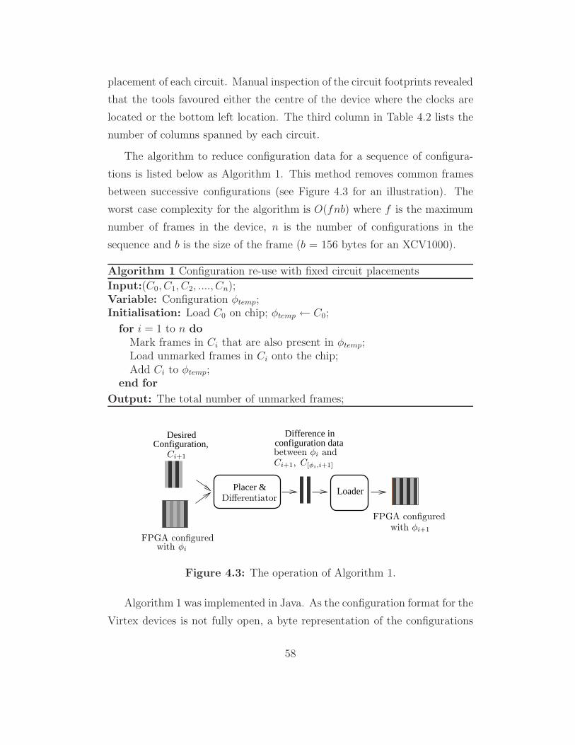
placement of each circuit. Manual inspection of the circuit footprints revealed
that the tools favoured either the centre of the device where the clocks are
located or the bottom left location. The third column in Table 4.2 lists the
number of columns spanned by each circuit.
The algorithm to reduce configuration data for a sequence of configura-
tions is listed below as Algorithm 1. This method removes common frames
between successive configurations (see Figure 4.3 for an illustration). The
worst case complexity for the algorithm is O(fnb) where f is the maximum
number of frames in the device, n is the number of configurations in the
sequence and b is the size of the frame (b = 156 bytes for an XCV1000).
Algorithm 1 Configuration re-use with fixed circuit placements
Input:(C0, C1, C2, ...., Cn);Variable: Configuration φtemp;Initialisation: Load C0 on chip; φtemp ← C0;
for i = 1 to n doMark frames in Ci that are also present in φtemp;Load unmarked frames in Ci onto the chip;Add Ci to φtemp;
end for
Output: The total number of unmarked frames;
DesiredConfiguration,
Placer &
Difference inconfiguration data
Loader
Ci+1
FPGA configuredwith φi
FPGA configuredwith φi+1
Ci+1, C[φi,i+1]
between φi and
Differentiator
Figure 4.3: The operation of Algorithm 1.
Algorithm 1 was implemented in Java. As the configuration format for the
Virtex devices is not fully open, a byte representation of the configurations
58

was first generated using JBits. Only the frames that lay within the column
boundaries of each circuit were considered. Non-null BRAM frames for each
circuit configuration were also included. It should be noted that Algorithm 1
removes common frames between successive configurations only if the frames
lie at the same addresses. If two successive circuits do not overlap then the
frames from the previous circuit will remain intact in the next configuration
state. It is assumed that these extraneous frames have no impact on the
operation of the required circuit.
Algorithm 1 was applied on a thousand random sequences of the thir-
teen cores listed in Table 4.2. A vector containing thirteen random numbers
between zero and twelve was generated using Java’s Math.random() method
and the configuration files were read in the same sequence as specified in the
vector. This procedure was then iterated a thousand times. It should be
noted that Algorithm 1 replaces on-chip null frames with non-null frames,
and vice versa, if successive configurations mutually span a region of the
device.
4.2.2 Results
There were 18,008 frames present in the input sequence (358 columns × 48
frames per column +824 non-null BRAM frames). Algorithm 1 removed 229
on average with a standard deviation of 110 frames. The resulting reduction
in reconfiguration time was calculated to be about 1%.
4.2.3 Analysis
There can be three reasons for this relatively small improvement: there were
not many common frames to remove; there were common frames but they
did not occur in consecutive configurations; and there were common frames
but they did not occupy the same column/frame position in the respective
configurations. The input configurations were further analysed to answer
59
these questions.
The configurations were scanned to determine the total number of unique
frames. This number turned out to be 16,916 frames. However, 1,092 frames
could still have been removed (or a 6% maximum possible reduction assum-
ing the cores were placed at positions that maximised their overlap and the
configuration sequence suited the placement). For the purposes of this anal-
ysis, two frames were considered similar only if they had the same data and
they were located at the same frame index within the respective columns.
Let us consider the second and third of the above mentioned reasons for
poor performance. As a thousand random permutations of the sequence were
generated and it was found that the standard deviation in the result was only
0.6%, the second reason does not seem plausible. Hence we are left with the
issue of frame alignability. By alignability it is meant that the frames could
be placed at the same column/frame address (thereby eliminating the frames
in the successive configurations once the first frame had been loaded). The
next section analyses this dimension of the problem.
4.3 Reducing Reconfiguration Cost with 1D
Placement Freedom
This section analyses the issue of frame alignability by allowing one-
dimensional placement freedom of the circuit. A greedy heuristic is eval-
uated and it is shown that allowing one-dimensional placement freedom does
not increase performance significantly and that this result is less dependant
on the performance of the algorithm than on the spatial distribution of the
common data in the successive configurations.
60

4.3.1 Problem formulation
The variable circuit placement problem is to place each circuit core onto the
device such that the total number of configuration frames required for the
entire input sequence is minimised. The Virtex model needs to be simplified
for the ease of analysis. First, it is assumed that Virtex is homogeneous, i.e.
all CLB columns are identical. This means that if one simply copies configu-
ration data corresponding to a column of CLBs to another column, the same
circuit should result at the copied location as in the original location. Sec-
ond, artifacts such as Block RAMs (BRAMs) are ignored as they introduce
asymmetries at the configuration data level. Third, a circuit’s connections
to the IO pins are ignored.
A circuit’s boundary is specified at its configuration data level. Each
partial configuration (subsequently referred to as a configuration in this sec-
tion) forms a contiguous set of frames meaning that each configuration has a
leftmost column/frame address and a rightmost column/frame address. The
placement freedom of a configuration, Ci, is thus given by c-|Ci| + 1 where
c is the total number of columns in the device and |Ci| is the number of
column spanned by Ci. The placement freedom corresponds to all legal col-
umn addresses, 1...c− |Ci|+ 1, for the leftmost column of the configuration.
The configurations can only be shifted by a multiple of columns. This means
that if a particular frame is at position x within a column then it will occupy
the same position in any column when the configuration is shifted across the
device.
Note: The partial reconfiguration problem with 1D placement freedom
seems similar to NP. complete multiple-sequence-alignment problem [32]. A
proof of its NP. completeness is left as an open problem.
4.3.2 A greedy solution
This section examines the performance of a greedy algorithm when applied
to the problem of configuration re-use with variable placements. Algorithm
61

2 places each configuration at a position that minimises the reconfiguration
data between it and the on-chip configuration. The worst case complexity
for this algorithm is O(f 2nb) where f is the maximum number of frames in
the device, n is the number of configurations in the sequence and b is the size
of the frame.
The benchmark circuits were considered again. The number of columns
spanned by each circuit is given in Table 4.2. A hundred different per-
mutations of the input sequence of configurations was generated. For each
sequence, each circuit was greedily placed at the location where the number
of frames between it and the current on-chip configuration was maximised.
It should be noted that frames from the previous configurations were not
cleared and it was assumed that the circuit is still operational.
With an initial total reconfiguration cost of 17,184 frames, the program
removed 579 frames on average, resulting in about 3% reduction in configu-
ration data (standard deviation = 154 frames).
It was found that even though there can be common frames among con-
figurations, they might not be alignable due to physical constraints on the
configuration placements. Please consider Figure 4.4, in which two configura-
tions Ci and Ci+1 are shown on a device with only one frame per column. Let
the common frames between the two be located at opposite ends as shown
by the lighter regions (the blocks numbered 1). It is clear that because of
constraints on the placement freedom the two configurations cannot be placed
such that the common frames of Ci+1 are aligned with those of Ci. Thus,
the common frames of Ci+1 should be considered to be unique. A simple
algorithm to detect such non-alignability was developed.
The algorithm operates on frames that occur more than once in the overall
sequence. It takes one such frame at a time and creates n bit vectors each
of size equal to the maximum number of frames the device can have. If the
frame occurs in the ith configuration, 0 ≤ i ≤ n, it marks those bits of the
ith vector where this frame can possibly be placed. Finally, it traverses the
62

Algorithm 2 Configuration re-use with variable circuit placements
Input:(C0, C1, C2, ...., Cn);Variable: Configuration φtemp; int minCost,minPlacement,#framesInitialisation: Load C0 on chip; φtemp ← C0;
for i = 1 to n dominCost← ∞;for j = 1 to placementFreedom(i) do
Try placing Ci at j;#frames = number of frames in Ci but not in φtemp;if #frames < minCost then
minPlacement = j;minCost = #frames;
end ifend forPlace Ci at minPlacement;Mark frames in Ci that are also present in φtemp;Load unmarked frames in Ci onto the chip;Add Ci to φtemp;
end for
Output: The total number of unmarked frames;
1
1
Ci+1
Ci
Max Number of Columns
Figure 4.4: Explaining the non-alignability of the common frames.
63

sequence from the start and performs an AND operation between successive
vectors. The resulting vector is examined. If it contains all zeros than each
occurance of the frame in the configurations is classified as unique. The
algorithm simply ignores the configurations that do not contain the frame
under consideration. It should be noted that this is a highly optimistic
measurement of frame alignability. However, a precise measurement involves
actually solving the variable circuit placement problem.
The above analysis was performed for 100 random permutations of the
sequence listed in Table 4.2. It was found that there were 16,532 actual
unique CLB frames and after running the alignability test, this number rose
to 16,741 (or almost 97%) — partly explaining the unexpectedly poor re-
duction in cost. Note that the BRAM frames were not considered in this
analysis.
Max Number of Columns
1
1 2
2
Ci
Ci+1
Figure 4.5: An example of frame interlocking.
In the case of an FPGA there exists another kind of non-alignability that
can be defined as frame-interlocking. As an example, consider Figure 4.5.
Shown are common frames numbered 1 and 2. Notice that we can either
align 1’s (resulting in a misalignment of 2’s) or vice versa but we cannot
align both simultaneously. Since no efficient solution to detect such frame-
interlocking was found, a tight lower bound on the optimal cost was not
computed. The reported cost estimates therefore remain optimistic. The
next section shows that:
• The absolute lower bound on the number of unique frames (whether
alignable or not) can be drastically reduced if we divide a frame into
sub-frames and allow them to be loaded independently.
64

3 12
1 2 1 2 3
32
2 3 1 2 3
7
3 frames
2 frames
sub−frames
that differthose subframeseliminates all but configuration re−useFine grained
Coarse grained
ConfigurationInput
to reload Frame 1eliminates the needconfiguration re−use
3
Figure 4.6: Coarse vs. fine-grained partial reconfiguration.
• The greedy method of placing the configurations, if such freedom is
allowed, is a reasonable solution in practice.
4.4 The Impact of Configuration Granularity
The smallest amount of configuration data that must be written into con-
figuration memory will be referred to as configuration granularity. This is a
similar concept to word size in conventional SRAMs.
The technique presented so far performed a frame-by-frame comparison.
Thus an entire frame had to be loaded even if there was only a single bit
difference with the copy already in configuration memory. Let us now break
the frames into smaller sub-frames and re-apply the partial reconfiguration
technique assuming that the sub-frames can be loaded independently (Figure
65
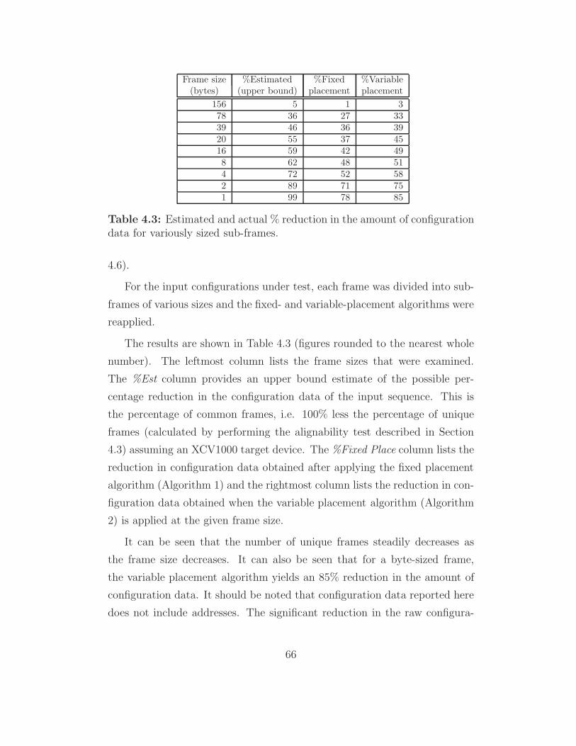
Frame size %Estimated %Fixed %Variable(bytes) (upper bound) placement placement
156 5 1 378 36 27 3339 46 36 3920 55 37 4516 59 42 498 62 48 514 72 52 582 89 71 751 99 78 85
Table 4.3: Estimated and actual % reduction in the amount of configurationdata for variously sized sub-frames.
4.6).
For the input configurations under test, each frame was divided into sub-
frames of various sizes and the fixed- and variable-placement algorithms were
reapplied.
The results are shown in Table 4.3 (figures rounded to the nearest whole
number). The leftmost column lists the frame sizes that were examined.
The %Est column provides an upper bound estimate of the possible per-
centage reduction in the configuration data of the input sequence. This is
the percentage of common frames, i.e. 100% less the percentage of unique
frames (calculated by performing the alignability test described in Section
4.3) assuming an XCV1000 target device. The %Fixed Place column lists the
reduction in configuration data obtained after applying the fixed placement
algorithm (Algorithm 1) and the rightmost column lists the reduction in con-
figuration data obtained when the variable placement algorithm (Algorithm
2) is applied at the given frame size.
It can be seen that the number of unique frames steadily decreases as
the frame size decreases. It can also be seen that for a byte-sized frame,
the variable placement algorithm yields an 85% reduction in the amount of
configuration data. It should be noted that configuration data reported here
does not include addresses. The significant reduction in the raw configura-
66
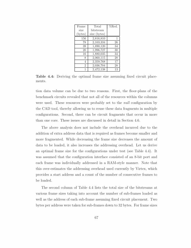
Frame Total %Red.size bitstream
(bytes) size (bytes)156 2,816,810 178 2,103,334 2639 1,890,120 3420 1,996,727 3016 1,880,035 348 2,060,115 284 2,359,768 172 2,036,704 281 2,472,138 13
Table 4.4: Deriving the optimal frame size assuming fixed circuit place-ments.
tion data volume can be due to two reasons. First, the floor-plans of the
benchmark circuits revealed that not all of the resources within the columns
were used. These resources were probably set to the null configuration by
the CAD tool, thereby allowing us to reuse these data fragments in multiple
configurations. Second, there can be circuit fragments that occur in more
than one core. These issues are discussed in detail in Section 4.6.
The above analysis does not include the overhead incurred due to the
addition of extra address data that is required as frames become smaller and
more fragmented. While decreasing the frame size decreases the amount of
data to be loaded, it also increases the addressing overhead. Let us derive
an optimal frame size for the configurations under test (see Table 4.4). It
was assumed that the configuration interface consisted of an 8-bit port and
each frame was individually addressed in a RAM-style manner. Note that
this over-estimates the addressing overhead used currently by Virtex, which
provides a start address and a count of the number of consecutive frames to
be loaded.
The second column of Table 4.4 lists the total size of the bitstreams at
various frame sizes taking into account the number of sub-frames loaded as
well as the address of each sub-frame assuming fixed circuit placement. Two
bytes per address were taken for sub-frames down to 32 bytes. For frame sizes
67

of less than 16 bytes 3 address bytes were added per sub-frame written. The
last column lists the overall percentage reduction compared to the current
Virtex. Table 4.4 suggests that a frame size of 39 bytes, or one quarter the
current Virtex frame size, is optimal since it offers good compression with
little address overhead.
The main conclusions from the above analysis are as follows. Firstly,
for relatively fine-grained logic fabrics such as Virtex, fine-grained, random
access to the configuration memory is needed in order to adequately exploit
the redundancy present in configuration data. Secondly, the actual reduction
achievable is also determined by the addressing overhead which increases
significantly as the unit of configuration is reduced and the number of those
units increase. Section 4.7 examines alternative addressing schemes. Thirdly,
introducing placement freedom does reduce the amount of reconfiguration
data but not significantly. Lastly, the relatively simple and quick greedy
strategies we explored provided reasonable reductions in overall configuration
bitstream sizes.
4.5 Sources of Redundancy in Inter-Circuit
Configurations
This section explains the results presented in the previous section. From
Table 4.2 it is clear that most circuits used only a small fraction of CLB
resources available in an XCV1000. It is likely that the CAD tool filled in
the unused portions of the configuration with null data. This gave rise to
a hypothesis that what was actually removed between the configurations is
nothing but null bitstream data. Simple experiments confirmed this hypoth-
esis.
68
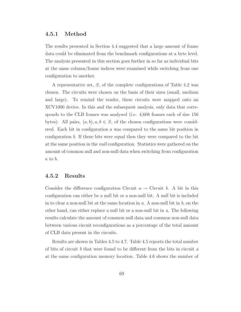
4.5.1 Method
The results presented in Section 4.4 suggested that a large amount of frame
data could be eliminated from the benchmark configurations at a byte level.
The analysis presented in this section goes further in so far as individual bits
at the same column/frame indices were examined while switching from one
configuration to another.
A representative set, S, of the complete configurations of Table 4.2 was
chosen. The circuits were chosen on the basis of their sizes (small, medium
and large). To remind the reader, these circuits were mapped onto an
XCV1000 device. In this and the subsequent analysis, only data that corre-
sponds to the CLB frames was analysed (i.e. 4,608 frames each of size 156
bytes). All pairs, (a, b), a, b ∈ S, of the chosen configurations were consid-
ered. Each bit in configuration a was compared to the same bit position in
configuration b. If these bits were equal then they were compared to the bit
at the same position in the null configuration. Statistics were gathered on the
amount of common null and non-null data when switching from configuration
a to b.
4.5.2 Results
Consider the difference configuration Circuit a → Circuit b. A bit in this
configuration can either be a null bit or a non-null bit. A null bit is included
in to clear a non-null bit at the same location in a. A non-null bit in b, on the
other hand, can either replace a null bit or a non-null bit in a. The following
results calculate the amount of common null data and common non-null data
between various circuit reconfigurations as a percentage of the total amount
of CLB data present in the circuits.
Results are shown in Tables 4.5 to 4.7. Table 4.5 reports the total number
of bits of circuit b that were found to be different from the bits in circuit a
at the same configuration memory location. Table 4.6 shows the number of
69

null bits that were common between circuit a and circuit b as a percentage
of the total number of frame bits in the device. For example, 145,570 bits
were found to be different when cordic was switched to blue tooth (Table
4.5). This means that 5,605,214 bits were found to be common between the
two configurations (there are 5,750,784 bits in the CLB configuration of an
XCV1000). Out of these common bits, 5,601,264 bits were found to be null
bits (or 97.5% of 5,750,784 bits). Table 4.7 shows similar values for non-null
bits.
In Table 4.6, values corresponding to circuit a → circuit b where a = b
show the total number of null bits in the configuration as a percentage of the
total number of CLB frame bits. For example, from Table 4.5, we see that
there are 101,776 non-null bits in blue tooth. Thus, there are 5,649,008 null
bits (98.2% of 5,750,784). Similar comments apply to the diagonal elements
of Table 4.7. Notice that the null bits that overwrite non-null bits, and vice
versa, are not included in this analysis. Thus, the respective columns of
Tables 4.6 and 4.7 do not add to 100.
4.5.3 Analysis
The results shown in Tables 4.5-4.7 confirm the hypothesis that the major
source of inter-configuration redundancy is simply null data filled in by the
CAD tool (Table 4.6). From these tables it can inferred that when a circuit
was replaced by another, only a small number of the resources share the same
non-null settings.
4.6 Analysing Default-state reconfiguration
This sections broadens the analysis presented in the previous sections. The
experiments so far suggest that a circuit makes a small number of changes
to the default configuration state of the device. One metric to measure the
size of this change can be to count the number of non-null bits in a given
70
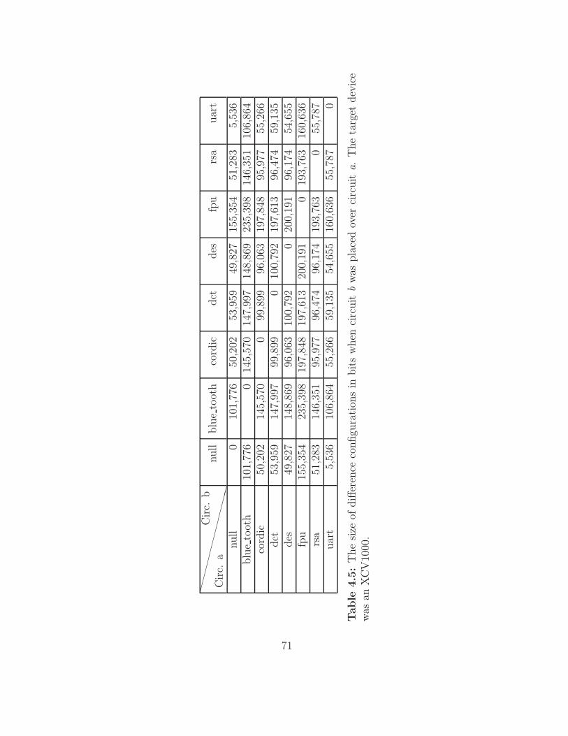
��
��
��
��
��
��
Cir
c.a
Cir
c.b
null
blu
eto
oth
cord
icdct
des
fpu
rsa
uar
t
null
010
1,77
650
,202
53,9
5949
,827
155,
354
51,2
835,
536
blu
eto
oth
101,
776
014
5,57
014
7,99
714
8,86
923
5,39
814
6,35
110
6,86
4co
rdic
50,2
0214
5,57
00
99,8
9996
,063
197,
848
95,9
7755
,266
dct
53,9
5914
7,99
799
,899
010
0,79
219
7,61
396
,474
59,1
35des
49,8
2714
8,86
996
,063
100,
792
020
0,19
196
,174
54,6
55fp
u15
5,35
423
5,39
819
7,84
819
7,61
320
0,19
10
193,
763
160,
636
rsa
51,2
8314
6,35
195
,977
96,4
7496
,174
193,
763
055
,787
uar
t5,
536
106,
864
55,2
6659
,135
54,6
5516
0,63
655
,787
0
Table
4.5
:T
he
size
ofdiff
eren
ceco
nfigu
rati
ons
inbits
when
circ
uit
bw
aspla
ced
over
circ
uit
a.
The
targ
etdev
ice
was
anX
CV
1000
.
71
��
��
��
��
��
��
Cir
c.a
Cir
c.b
blu
eto
oth
cord
icdct
des
fpu
rsa
uar
t
blu
eto
oth
98.2
97.4
97.3
97.3
95.7
97.4
98.1
cord
ic97
.499
.198
.298
.396
.598
.299
.0dct
97.3
98.2
99.0
98.2
96.4
98.2
99.0
des
97.4
98.3
98.2
99.1
96.5
98.3
99.0
fpu
95.7
96.5
96.4
96.5
97.3
96.5
97.0
rsa
97.4
98.2
98.2
98.3
96.5
99.1
99.0
uar
t98
.199
.099
.099
.097
.099
.099
.9
Table
4.6
:T
he
rela
tive
num
ber
ofnull
bits
inth
ediff
eren
ceco
nfigu
rati
ons
(circu
ita→
circ
uit
b)as
aper
centa
geof
the
tota
lnum
ber
ofC
LB
-fra
me
bit
sin
the
dev
ice.
The
targ
etdev
ice
was
anX
CV
1000
.A
llnum
ber
sar
ero
unded
toon
edec
imal
dig
it.
72

��
��
��
��
��
��
Cir
c.a
Cir
c.b
blu
eto
oth
cord
icdct
des
fpu
rsa
uar
t
blu
eto
oth
1.8
0.1
0.1
0.0
0.2
0.1
0.0
cord
ic0.
11.
00.
00.
00.
10.
00.
0dct
0.1
0.0
1.0
0.0
0.1
0.1
0.0
des
0.0
0.0
0.0
1.0
0.0
0.0
0.0
fpu
0.2
0.1
0.1
0.0
2.7
0.1
0.0
rsa
0.1
0.1
0.1
0.0
0.1
0.9
0.0
uar
t0.
00.
00.
00.
00.
00.
00.
1
Table
4.7
:T
he
rela
tive
num
ber
ofnon-n
ull
bitsin
the
diff
eren
ceco
nfigu
rati
ons(c
ircu
ita→
circ
uit
b)as
aper
centa
geof
the
tota
lnum
ber
ofC
LB
-fra
me
bit
sin
the
dev
ice.
The
targ
etdev
ice
was
anX
CV
1000
.A
llnum
ber
sar
ero
unded
toon
edec
imal
dig
it.
73

configuration. This was done in the previous section for a selection of circuits
and shown to be small compared to the total number of bits present in the
complete configuration. This section investigates the impact of FPGA size
on the number of bit flips that are introduced by a circuit to the default
configuration state. This section establishes that the amount of non-null
configuration data of typical circuits is almost independent of the target
device size, or circuit domain. This can be best observed at a configuration
granularity of a single bit.
The benchmark circuit set (Table 4.2) was enlarged to accommodate a
wider set of circuits as listed in Table 4.8. The circuits convolution and
comparator were dropped due to their insignificant sizes. The circuit adder
was replaced with add-sub (adder/subtracter). This benchmark set is used
in all subsequent experiments.
Each circuit in the benchmark set was mapped onto variously sized Vir-
tex devices and the number of non-null CLB frames was counted. Results for
three devices are shown in the table. A ‘-’ in the XCV200 column means that
the corresponding circuit could not be mapped onto that device. The last
three columns in Table 4.8 show the amount of CLB frame data needed under
various device sizes if one uses the current frame-oriented partial reconfig-
uration of Virtex and removes all null frames from the given configuration.
These results show that the amount of partial configuration data needed for
a circuit increases when the circuit is mapped to a larger device despite set-
ting the ISE place and route tools to optimise for area. This is expected as
the frame size increases with the device size. Refer to Table 4.1 for relevant
parameters of the three Virtex devices.
4.6.1 The impact of configuration granularity
The experiments of Section 4.2 show that the redundant data between any
two configurations can best be removed at fine granularities. This section
shows that given an isolated configuration, the null data can best be removed
74

Circuit #4-LUTs #Nets #IOB #Non-null CLB framesXCV200 XCV400 XCV1000
encoder [120] 127 456 127 630 696 755uart [120] 93 467 52 869 1,031 1017asyn-fifo [120] 22 584 69 1,324 1,579 1,823add-sub [120] 49 344 197 - 1,545 1,7392compl-1 [120] N/A N/A N/A - 1,726 1,941spi [117] 150 796 150 1,086 1,163 1,349fir-srg [68] 216 726 216 585 632 1,347dfir [120] 179 782 43 1,078 1,161 935cic3r32 [68] 152 736 152 1,055 939 482ccmul [68] 262 905 58 1,051 1,055 1,007bin-decod [120] 288 1,249 200 - 2,263 2,9642compl-2 [120] 129 388 257 - 2,180 2,435ammod [68] 271 990 45 1,151 1,655 2,335bfproc [68] 418 1,347 90 1,131 2,159 3,063costLUT [120] 547 2,574 45 1,184 1,526 421gpio [117] 507 3,022 207 1,762 2,127 2,823irr [68] 894 2,907 894 1,695 1,492 1,588des [117] 132 5,060 189 - 2,590 4,492cordic [117] 1112 4,745 73 1,969 1,796 2,439rsa [117] 1114 5,039 131 1,797 2,125 2,298dct [120] 1064 5,327 78 1,874 2,314 1,903blue-th [117] 2,711 11,152 84 - 2,879 4,199vfft1024 [68] 3,101 11,405 N/A - 2,781 3,079fpu [117] 3,914 13,522 109 - 2,880 3,655
Table 4.8: The benchmark circuits and their parameters of interest.
75

at 1 bit granularity. If the granularity is increased then some null data
must be included and the amount of this extra data is proportional to the
granularity.
Method
All circuits in the benchmark set that could be mapped onto an XCV100
device were examined (see Appendix B for a list of these circuits). Complete
configurations corresponding to each circuit were generated. Only CLB frame
data was considered. Each configuration was then compared, bit-by-bit, with
the corresponding null configuration for the device. The number of bits, k1,
that were different in the input configuration from the corresponding bit in
the null configuration was determined. In other words, the size of the differ-
ence configuration was determined assuming 1-bit configuration granularity.
The experiment was repeated assuming 2-bit configuration granularity. This
time, both bits in a particular data fragment were required to be equal to
their null counter-parts in order to be removed. The number of non-null
units, k2, was determined for each circuit. Similarly, kg was determined for
granularities 4, 8 and 16. The mean of kg ∗ g/k1 was calculated over all
circuits that could be mapped onto an XCV100 for each value of g.
Results
Figure 4.7 shows the amount of configuration data needed at granularity g
relative to the amount needed at granularity a of a single bit. This figure
clearly shows that as g is increased, the total amount of CLB frame data also
increases. In other words, more and more null data is incorporated as the
data granularity is increased. Results for the circuits on larger devices is the
same.
76

1
2
3
4
5
6
7
8
9
0 2 4 6 8 10 12 14 16
Mea
n am
ount
of d
ata
(mea
n k_
g*g/
k_1)
Granularity g (bits)
"k_g_xcv100"
Figure 4.7: The amount of configuration data needed at granularity g rel-ative to the amount of data needed at a granularity of a single bit.
Analysis
One way of interpreting Figure 4.7 is that the non-null bits in typical config-
uration are spatially distributed in an almost uniform manner. This feature
of configuration data will be discussed in more detail in Chapter 6.
4.6.2 The impact of device size
This experiment complements the above experiments by examining the com-
bined impact of the device size and configuration granularity.
Method
Each circuit in the benchmark set was mapped from the smallest possible
Virtex device to the largest available device, i.e. XCV1000. Complete config-
urations corresponding to each circuit on each device were generated. Only
77
CLB frame data was considered. Each configuration was then compared,
bit-by-bit, with the corresponding null configuration of the same size. The
number of bits, k1, that were different in the input configuration from the
corresponding bit in the null configuration was determined. The mean and
standard deviation in k1 across the range of devices was calculated. A similar
exercise was performed for k4. Tables B.1 and B.2 in Appendix B show the
complete results.
Results
Table 4.9 shows the results. It is clear that the standard deviation in k1
is less than that in k4, not only in aggregate size but also with respect to
the total amount of non-null data at that granularity. This result essentially
generalises the result presented in the previous subsection.
4.6.3 The impact of circuit size
Table 4.9 shows that the amount of non-null frame data varies considerably
from circuit to circuit. In order to explain this result the sizes of the circuits
were considered. This section shows that the amount of non-null frame data
for a circuit is almost linearly proportional to its size.
Method
Measuring a circuit’s size at the configuration data level poses practical prob-
lems. This is because commercial CAD tools do not provide detailed reports
on the amount of resources used by an input circuit. For example, while Xil-
inx tools report on the number of LUTs used by a circuit they do not report
on the number of programmable interconnect points (PIPs) used. In any
case, a technology-mapped netlist can be considered to be a good reference
for measuring a circuit’s size even though it does not take account of the
number of physical wire segments needed to implement each logical wire.
78

Circuit k1 Std-dev in k1 k4 Std-dev in k4
(bits) (bits) (bits) (bits)encoder 4,307 88 12,668 415uart 5,281 162 14,951 539asyn fifo 5,726 239 18,276 773adder-sub 6,076 231 20,732 7982compl-1 8,089 627 28,058 2,504spi 7,947 106 23,103 240fir-srg 8,284 240 23,334 373dfir 8,393 266 23,939 656cic3r32 8,867 276 25,393 871ccmul 9,937 223 29,786 975bin-decod 10,384 974 35,138 3,4332compl-2 11,935 689 41,391 2,770ammod 11,714 187 34,719 1,142bfproc 15,000 558 44,453 2,846costLUT 16,376 209 48,486 753gpio 31,290 701 95,179 3,215irr 34,376 699 99,757 2,191des 48,644 850 145,725 4,201cordic 49,466 518 138,526 961rsa 50,138 868 146,533 2,888dct 53,188 794 147,532 3,257blue-th 101,640 539 293,542 3,285vfft1024 113,956 1,130 315,966 2,769fpu 155,672 1,336 454,568 3,531Mean 31,114 501 90,609 1,819
Table 4.9: Comparing the change in the amount of non-null data for thesame circuit mapped onto variously sized devices.
79

A closer inspection of typical technology-mapped netlists revealed that
circuits use various FPGA resources in various proportions. One circuit
might use a large number of LUTs but only a small number of IO ports. On
the other hand, some circuits tend to be IO-limited but use logic resources
sparsely. It was thus clear that assigning a single number that specifies the
resource utilisation of a circuit was likely to hide away important details at
the lower level. Therefore three different parameters were used to specify a
circuit’s size: number of 4-LUTs (found from the technology map report),
number of IO blocks and the number of nets in the input technology-mapped
netlist. Table 4.8 shows the benchmark circuits and their sizes.
The benchmark configurations targeting an XCV400 device were then
analysed. Again, only CLB frames were examined. As was discussed earlier,
a Virtex frame contributes thirty-six bits to the top and bottom IOBs and
eighteen bits to each CLB. The IOBs were ignored and each eighteen-bit
CLB fragment was examined. Out of these eighteen bits, the top nine are
classified as routing bits (corresponding to single and hex switches) and the
remaining nine as logic bits (refer to Section 3.2.1 for a description of the
Virtex’ frame structure). These bits were then compared to the null bits at
the same location and non-null routing and non-null logic bits were counted.
Notice that this analysis is only roughly accurate as the exact structure of
the frames is not described in the Virtex data-sheet. All CLB frames in each
configuration were processed in this manner.
Results
Figure 4.8 shows the result of correlating the amount of non-null routing data
with the number of nets in the input circuit. Figure 4.9 shows the result of
correlating the amount of non-null logic data with the number of 4-LUTs in
the input circuit.
80

0
20000
40000
60000
80000
100000
120000
140000
0 2000 4000 6000 8000 10000 12000 14000
#Non
-nul
l rou
ting
bits
#Nets
f(x)g(x)
"routing-net-corr"
Figure 4.8: Correlating the number of nets with the total number of non-null routing bits used to configure an XCV400 with the benchmark circuits.
Analysis
The graphs in Figures 4.8 and 4.9 clearly show an almost linear dependency
between the circuit’s size, measured in terms of the number of nets or 4-
LUTs it contains, and the number of bits that it flips in the default-state
configuration. Figure 4.8 also plots a linear function f(x) = 9x and the best
fitting curve g(x) = 0.0002x2 + 6.8786x + 1599.6. That the data is slightly
super-linear for routing bits can be explained by the increasing likelihood
that additional routing segments are needed to implement the nets as the
device becomes increasingly congested. The best fitting curve in Figure 4.9
corresponds to g(x) = 3.5891x + 497.08.
In summary:
• The amount of non-null data in a typical Virtex configuration is small
compared to the total amount of CLB frame data. The null data from a
81
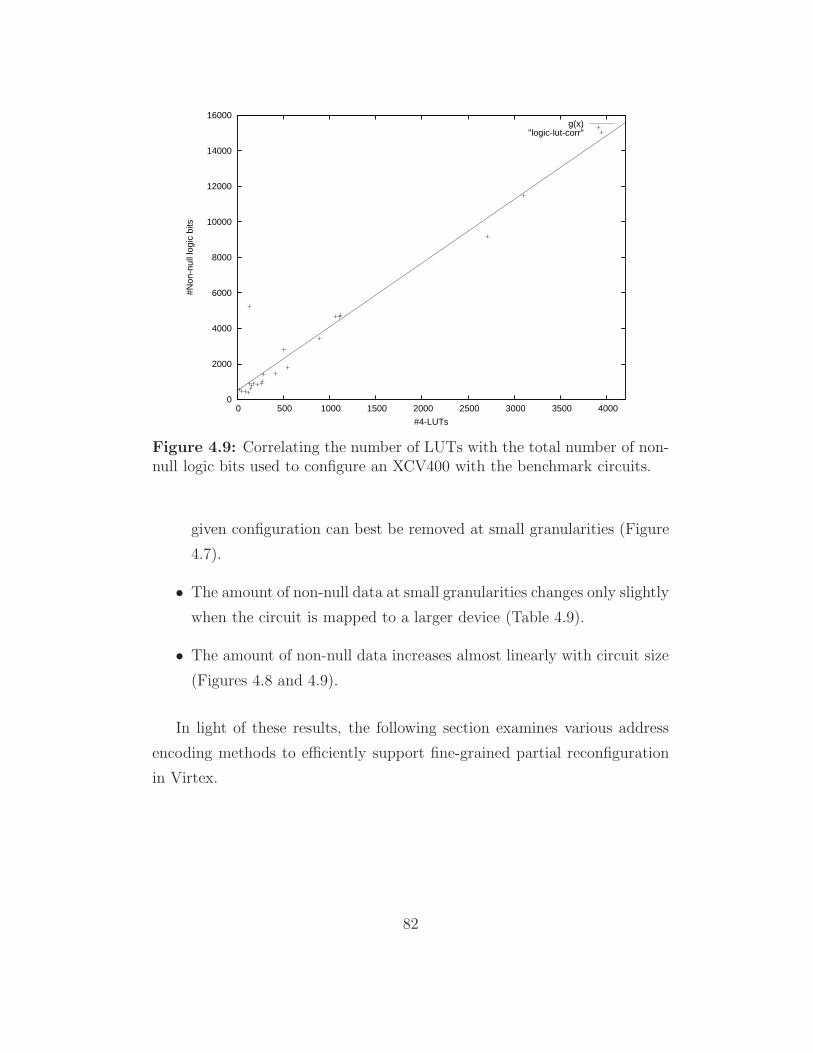
0
2000
4000
6000
8000
10000
12000
14000
16000
0 500 1000 1500 2000 2500 3000 3500 4000
#Non
-nul
l log
ic b
its
#4-LUTs
g(x)"logic-lut-corr"
Figure 4.9: Correlating the number of LUTs with the total number of non-null logic bits used to configure an XCV400 with the benchmark circuits.
given configuration can best be removed at small granularities (Figure
4.7).
• The amount of non-null data at small granularities changes only slightly
when the circuit is mapped to a larger device (Table 4.9).
• The amount of non-null data increases almost linearly with circuit size
(Figures 4.8 and 4.9).
In light of these results, the following section examines various address
encoding methods to efficiently support fine-grained partial reconfiguration
in Virtex.
82

4.7 The Configuration Addressing Problem
Reducing the configuration unit size from a frame to a few bytes substan-
tially increases the amount of address data that needs to be loaded and the
addressing overhead therefore limits the benefits of fine-grained partial recon-
figuration. The analysis in Section 4.4 assumed a RAM-style configuration
memory in which each sub-frame had its own address. Taking the addressing
overhead into account, it was found that the potential 78% reduction in con-
figuration data was diminished to a maximum possible 34% overall reduction
in bitstream size. Due to increased addressing overhead as sub-frame size is
reduced, this best possible improvement over vanilla Virtex was achieved at
a sub-frame spanning one quarter of the column-high frame rather than at
the byte-level granularity, when maximum reduction in raw frame data was
found to be possible. Thus, the analysis so far suggests that if one can find
an efficient method of compressing address data then reconfiguration time
can be decreased.
Reducing the configuration addressing overhead is referred to as the
configuration addressing problem and it can be described as follows:
The configuration addressing problem: Let there be n configura-
tion registers numbered 1 to n in a device. Suppose k arbitrary registers
are selected to be accessed such that k <= n. Thus we are given a set of k
locations, where each location is given a number between 1 and n inclusive.
The problem is to derive an efficient encoding of the set of k locations
chosen. The criteria for efficiency are that the encoding must be small, so
that it takes little time to load onto the device, and that its decoding is
simple, so that it is possible to facilitate rapid decoding in hardware.
The XC6200 family supported partial reconfiguration at the byte level in
a RAM-like manner [128]. The RAM model requires O(log2(n)) address bits
per configuration register. Thus, the address data requires O(klog2(n)) time
to load onto the device where k is the number of registers to be updated. As
83

n and k increase, the amount of address data in this model grows substan-
tially. The wildcarding mechanism for the XC6200 devices can be seen as a
method for compressing RAM address data. The Virtex devices, much larger
than XC6200s, offer a two-fold solution to this problem [123]. First, the con-
figuration granularity was increased by 50 to 100 times compared to XC6200
thereby keeping the total number of addressable units small. This solution,
however, limits partial reconfiguration as discussed above. Secondly, Virtex
introduced a DMA-style run-length addressing of the blocks of consecutive
frames having to be loaded. This model improves upon the RAM model
by a factor of k if all k frames are consecutive. In terms of address data
usage, the performance of the model approaches that of the RAM model for
isolated frames. This runlength compression has been applied in the con-
text of XC6200 devices in [38] and the authors have shown a reduction in
reconfiguration time by a factor of more than three.
The following section presents an analysis of various methods of encoding
address data for fine-grained partial configurations in the context of Virtex
devices and suggests that new addressing methods are required that are a
hybrid of the existing ones.
4.8 Evaluating Various Addressing Tech-
niques
This section presents an analysis of various address encoding techniques for
fine-grained partial configurations. One technique, the RAM method, was
previously assessed. This section examines two further methods. The first
compresses the RAM addresses using run-length encoding. This technique
will be referred to as the DMA method. The second technique is referred to
as vector addressing (VA).
The concept of VA is simple. Let us assume that a device contains a total
of n configuration sub-frames numbered from 1 to n. Define a bit vector of
84

size n to identify the set of sub-frames that is to be loaded onto the device.
The ith bit in this vector represents the address of the ith sub-frame register
where 1 ≤ i ≤ n. In this address vector, a bit is set to 1 if the corresponding
sub-frame is to be included in this configuration bitstream, otherwise it is
left unset at 0.
The experiments show that the RAM method is most suited to addressing
configuration data for sparse circuits on large devices and that the VA method
performs best when used to configure dense circuits on small devices. The
DMA technique was found to performs relatively poorly at compressing RAM
addresses.
Theoretical considerations
The RAM method requires log2(n) bits of data per configuration unit that
is included in the bitstream. The VA method, on the other hand, has a fixed
overhead of n bits. Let us suppose that k units need to be addressed. The
RAM method will require less data that the VA method when klog2(n) < n.
As changing configuration granularity changes n and k, both methods are
likely to perform differently under various conditions. The following section
examines this trade-off for the benchmark circuits.
Experimental Method
The CLB frames corresponding to each benchmark circuit were examined.
RAM addresses for all non-null configuration units were generated when the
configurations were partitioned into granularities ranging from 4 to 32 bits
in size. The minimum granularity was chosen to be 4 because the amount of
address data was prohibitively large for smaller granularities. The VA size
of the configuration was simply calculated by dividing the complete config-
uration size in bits by the assumed granularity. Note that the experiments
assume that the circuits are to be loaded onto a device already configured
with null configuration. The results of Section 4.6 indicate that there is little
85

additional overhead to be expected when the device is already configured
with a circuit.
Results
Tables 4.10 to 4.12 report on the results. Only the results for 8-bit granularity
and for devices XCV100, XCV400 and XCV1000 are shown. Complete results
can be found in Appendix B. The first column in these tables lists the
circuit used. The second column lists the amount of data needed under
the current Virtex model needed to configure the circuit (i.e. frame oriented
reconfiguration). This also includes the address overheads. The third column
lists the amount of new sub-frame data when configuration granularity was
reduced to 8 bits. The last three columns list the overall percentage reduction
in configuration data that is achieved compared to the current Virtex model
when the RAM, the DMA, and the VA addressing overheads are included.
Analysis
Tables 4.10 to 4.12 show that the RAM method performs better than the VA
method for sparse circuits or when the devices are large. As expected, the
VA method is better for dense circuits. For sparse circuits on large device,
VA even gives negative results. The reason for this is that VA is applied
at the device level, i.e. all bytes in the complete configuration are specified.
The performance of VA is likely to improve if it is combined with the RAM
method. A design of such a configuration memory architecture for Virtex is
the topic of the next chapter.
4.9 Chapter Summary
This chapter presented a detailed analysis of partial reconfiguration in Virtex.
The following key results were presented:
86

Circuit Virtex Frame RAM DMA VA(bits) (bits) %red. %red. %red.
encoder 297,920 20,848 78 73 66uart 304,192 26,536 73 68 65asyn-fifo 498,624 30,568 81 76 78add-sub - - - - -2compl-1 - - - - -spi 417,536 39,320 71 67 71fir-srg 203,840 39,656 39 34 41dfir 416,192 40,240 70 64 71cic3r32 399,616 43,384 66 59 69ccmul 382,144 47,648 61 56 66bin-decod - - - - -2compl-2 - - - - -ammod 401,408 57,440 55 49 66bfproc 502,208 70,952 56 48 70costLUT 505,344 84,120 48 37 67gpio - - - - -irr 588,224 163,544 13 9 58des - - - - -cordic - - - - -rsa - - - - -dct - - - - -blue-th - - - - -vfft1024 - - - - -fpu - - - - -
Table 4.10: Comparing various addressing schemes. Granularity = 8 bits.Target device = XCV100.
87
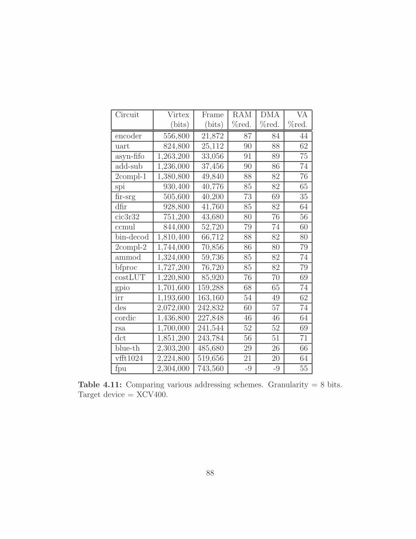
Circuit Virtex Frame RAM DMA VA(bits) (bits) %red. %red. %red.
encoder 556,800 21,872 87 84 44uart 824,800 25,112 90 88 62asyn-fifo 1,263,200 33,056 91 89 75add-sub 1,236,000 37,456 90 86 742compl-1 1,380,800 49,840 88 82 76spi 930,400 40,776 85 82 65fir-srg 505,600 40,200 73 69 35dfir 928,800 41,760 85 82 64cic3r32 751,200 43,680 80 76 56ccmul 844,000 52,720 79 74 60bin-decod 1,810,400 66,712 88 82 802compl-2 1,744,000 70,856 86 80 79ammod 1,324,000 59,736 85 82 74bfproc 1,727,200 76,720 85 82 79costLUT 1,220,800 85,920 76 70 69gpio 1,701,600 159,288 68 65 74irr 1,193,600 163,160 54 49 62des 2,072,000 242,832 60 57 74cordic 1,436,800 227,848 46 46 64rsa 1,700,000 241,544 52 52 69dct 1,851,200 243,784 56 51 71blue-th 2,303,200 485,680 29 26 66vfft1024 2,224,800 519,656 21 20 64fpu 2,304,000 743,560 -9 -9 55
Table 4.11: Comparing various addressing schemes. Granularity = 8 bits.Target device = XCV400.
88

Circuit Virtex Frame RAM DMA VA(bits) (bits) %red. %red. %red.
encoder 942,240 22,400 92 90 21uart 1,269,216 27,824 92 91 41asyn-fifo 2,275,104 34,208 95 93 67add-sub 2,170,272 38,864 94 91 652compl-1 2,422,368 61,424 91 87 68spi 1,683,552 39,064 92 91 55fir-srg 1,681,056 40,000 92 91 55dfir 1,166,880 41,872 87 86 35cic3r32 601,536 43,216 75 71 -27ccmul 1,256,736 53,776 85 82 39bin-decod 3,699,072 66,968 94 91 792compl-2 3,038,880 83,888 90 85 74ammod 2,914,080 64,840 92 90 73bfproc 3,822,624 85,920 92 90 79costLUT 525,408 80,200 47 36 -52gpio 3,523,104 172,360 83 80 75irr 1,981,824 164,136 71 68 55des 5,606,016 265,928 83 80 82cordic 3,043,872 232,520 73 72 69rsa 2,867,904 247,824 70 69 66dct 2,374,944 253,488 63 59 59blue-th 5,240,352 507,400 66 62 77vfft1024 3,842,592 529,624 52 48 68fpu 4,561,440 768,848 41 37 67
Table 4.12: Comparing various addressing schemes. Granularity = 8 bits.Target device = XCV1000.
89

• Major portions of typical configurations are essentially comprised of
null data.
• The null data is best removed at small configuration granularities.
• The amount of non-null configuration data depends mostly on the size
of the circuit and less on the size of the target device onto which it is
mapped.
• Fine-grained partial reconfiguration yields good reductions in configu-
ration bitstream size if the addressing overhead can be kept small.
• Various methods of addressing configuration data were analysed. The
binary address encoding is useful when the circuit is small relative to
the device size. Unary encoding of the address data is useful when
the circuit is large relative to the size of the device. Thus, a hybrid
approach should provide a reasonable overall performance.
The next chapter presents a new Virtex configuration memory design that
is derived from the analyses summarised above.
90
Chapter 5
New Configuration
Architectures for Virtex
5.1 Introduction
The previous chapter presented a detailed analysis of configuration data for a
set of benchmark circuits on Virtex devices. It attributed major redundancy
in the configuration data to the presence of null data that is inserted by
the CAD tool to reset the resources that are not used by the circuit at
hand. It was shown that such redundancy can be best removed at small
configuration granularities (ideally at a bit-level). Given that the current
Virtex implements a frame-oriented partial reconfiguration, where the frame
size can be as large as 156 bytes, an efficient new memory design is needed
that supports more fine-grained configuration updates. This chapter presents
new architectures for Virtex configuration memory that support byte-level
partial reconfiguration.
The goal is to upgrade the current Virtex configuration memory into
one that can be addressed in a fine-grained manner with minimal hardware
addition. This chapter starts by first presenting the current architecture
of the Virtex configuration memory (Section 5.2). This model is used as
91

the basis for the designs presented later. Section 5.3 presents the first new
architecture, ARCH-I which supports byte-level partial reconfiguration. It
does this by employing a read-modify-write method whereby on-chip frames
are read into a buffer, modified based on the supplied vector address and
then written back to their origin.
The limitation of the configuration re-use method, where on-chip config-
uration fragments are used to construct the later circuits, is that the user
must be aware of the current state of the configuration memory. It was
shown in Chapter 4 that what is re-used between various circuit reconfigu-
rations is essentially null data. This suggests a memory that automatically
inserts null data into the specified memory locations thereby eliminating the
need to know the current configuration state and thereby reducing the need
to load null data from off-chip. Section 5.4 presents ARCH-II which incor-
porates this feature. Finally, Section 5.5 discusses methods for parallelising
the configuration load process which is possible if the configuration port size
is increased. An area efficient architecture, ARCH-III, is presented, which is
shown to scale well with configuration port size.
5.2 Virtex Configuration Memory Internals
Xilinx holds two patents on configuration memories and these publicly avail-
able documents describe the internal details [73],[81] of Virtex configuration
memory. A Virtex device contains various registers for holding instructions,
frame data and frame addresses as shown in Figure 5.1. A configuration
state machine accepts various user commands such as read or write frames
and generates necessary control signals for the data path. The following dis-
cussion focuses on the configuration write operation with reference to Figure
5.1 (configuration reads are similar).
In order to write configuration data, the state machine is first issued with
a write-frames command. The user can write a block of consecutive frames by
92
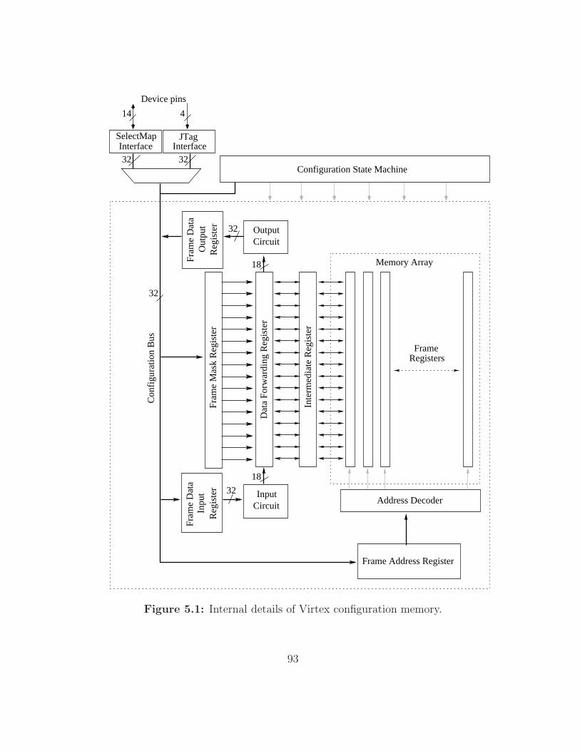
InputCircuit
InterfaceSelectMap JTag
Interface
CircuitOutput
Fram
e D
ata
Inpu
t R
egis
ter
Fram
e D
ata
Out
put
Reg
iste
r
Inte
rmed
iate
Reg
iste
r
Dat
a Fo
rwar
ding
Reg
iste
r
Fram
e M
ask
Reg
iste
r
Frame Address Register
Con
figu
ratio
n B
us
32
18
18
32
32
Address Decoder
RegistersFrame
Memory Array
32 32Configuration State Machine
14 4
Device pins
Figure 5.1: Internal details of Virtex configuration memory.
93

supplying the address of the first frame in the block followed by the number
of frames to follow. The user supplied address/count is transfered to the
frame address register (FAR). The FAR is incremented for each frame that is
loaded into the array. The FAR is directly connected to an address decoder
which generates the necessary control signals to select an entire frame register
for a write operation.
A Virtex device contains two interfaces for (re)configuration; SelectMAP
and JTAG. The SelectMap interface shares its pins with the general purpose
IO pins. This interface is 14 bits wide out of which 8 are data and the rest
are control pins. The JTAG interface has 4 dedicated pins. While JTAG can
also be used for (re)configuration, its main use is in device testing. A Vir-
tex FPGA internally contains a 32-bit wide configuration bus that connects
together various components. The user-supplied data is first assembled into
32-bit words before it is passed onto various internal registers.
The input frame data is first loaded into a shift register called the frame
data input register (FDRI)1 which buffers an entire frame. Once the FDRI is
full, the data is shifted into the data forwarding register via the input-circuit.
The input-circuit is used to align 32-bit words into multiples of 18 bits (in the
actual device two 18-bit words are produced at a time). This is achieved by
alternatively writing 32-bit words in two separate registers and then selecting
the next 36-bit word from the data available in these registers (Figure 5.2).
While data is shifted in from the FDRI to the data forwarding register, the
user shifts more frame data into the FDRI thereby pipelining the operation.
Once the data forwarding register is full, its contents are transfered in parallel
to an intermediate register and then to the selected frame register.
One of the patent documents describes a method by which one can read
a Virtex frame into the intermediate register and selectively modify its bytes
[81], but the Virtex data sheet does not provide any details of this operation.
In order to selectively modify a frame, it is first read into the intermediate
register. The mask register is then supplied with a bit mask of size f bits
1Xilinx uses the acronym FDRI instead of FDIR.
94
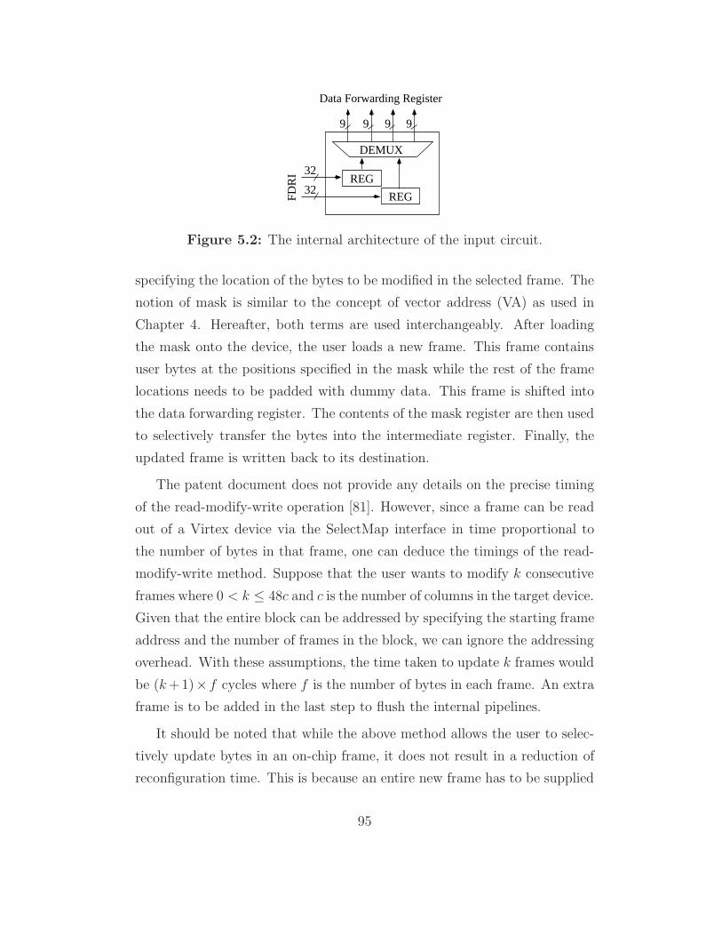
REG
REG
9 9 9 9
DEMUX
32
32
Data Forwarding Register
FDR
I
Figure 5.2: The internal architecture of the input circuit.
specifying the location of the bytes to be modified in the selected frame. The
notion of mask is similar to the concept of vector address (VA) as used in
Chapter 4. Hereafter, both terms are used interchangeably. After loading
the mask onto the device, the user loads a new frame. This frame contains
user bytes at the positions specified in the mask while the rest of the frame
locations needs to be padded with dummy data. This frame is shifted into
the data forwarding register. The contents of the mask register are then used
to selectively transfer the bytes into the intermediate register. Finally, the
updated frame is written back to its destination.
The patent document does not provide any details on the precise timing
of the read-modify-write operation [81]. However, since a frame can be read
out of a Virtex device via the SelectMap interface in time proportional to
the number of bytes in that frame, one can deduce the timings of the read-
modify-write method. Suppose that the user wants to modify k consecutive
frames where 0 < k ≤ 48c and c is the number of columns in the target device.
Given that the entire block can be addressed by specifying the starting frame
address and the number of frames in the block, we can ignore the addressing
overhead. With these assumptions, the time taken to update k frames would
be (k +1)× f cycles where f is the number of bytes in each frame. An extra
frame is to be added in the last step to flush the internal pipelines.
It should be noted that while the above method allows the user to selec-
tively update bytes in an on-chip frame, it does not result in a reduction of
reconfiguration time. This is because an entire new frame has to be supplied
95
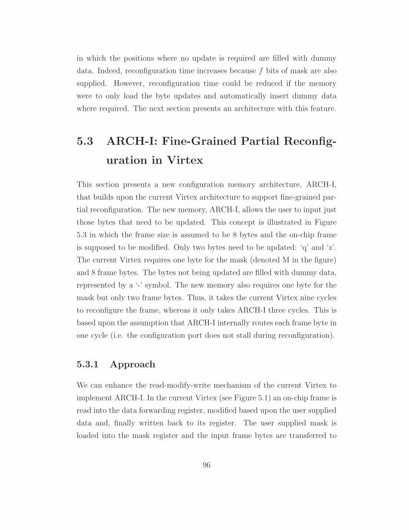
in which the positions where no update is required are filled with dummy
data. Indeed, reconfiguration time increases because f bits of mask are also
supplied. However, reconfiguration time could be reduced if the memory
were to only load the byte updates and automatically insert dummy data
where required. The next section presents an architecture with this feature.
5.3 ARCH-I: Fine-Grained Partial Reconfig-
uration in Virtex
This section presents a new configuration memory architecture, ARCH-I,
that builds upon the current Virtex architecture to support fine-grained par-
tial reconfiguration. The new memory, ARCH-I, allows the user to input just
those bytes that need to be updated. This concept is illustrated in Figure
5.3 in which the frame size is assumed to be 8 bytes and the on-chip frame
is supposed to be modified. Only two bytes need to be updated: ‘q’ and ‘z’.
The current Virtex requires one byte for the mask (denoted M in the figure)
and 8 frame bytes. The bytes not being updated are filled with dummy data,
represented by a ‘-’ symbol. The new memory also requires one byte for the
mask but only two frame bytes. Thus, it takes the current Virtex nine cycles
to reconfigure the frame, whereas it only takes ARCH-I three cycles. This is
based upon the assumption that ARCH-I internally routes each frame byte in
one cycle (i.e. the configuration port does not stall during reconfiguration).
5.3.1 Approach
We can enhance the read-modify-write mechanism of the current Virtex to
implement ARCH-I. In the current Virtex (see Figure 5.1) an on-chip frame is
read into the data forwarding register, modified based upon the user supplied
data and, finally written back to its register. The user supplied mask is
loaded into the mask register and the input frame bytes are transferred to
96
a b c d e f g h
q b c d e f g z
Virtex
q z
1 2 3 4 5 6 7 98
Required Frame
Mask (M)
Current Frame
1 0 0 0 0 0 0 1
ARCH−I
Time (cycles)
M
M q − − − − z−−
Figure 5.3: Comparing the operation of Virtex and ARCH-I.
the input circuit via the FDRI. We could implement ARCH-I by switching
the output of the input circuit to the correct locations in the data forwarding
register based on the user suppled mask. Figure 5.4 shows the part of the
Virtex model where the new switch would be inserted (compare with Figure
5.1). However, this approach has two drawbacks. Firstly, depending upon
the implementation, the input circuit can become complicated as it may be
the case that the bytes in an incoming 32-bit word are not contiguous in the
target frame. Secondly, the dimensions of the switch depend on the frame
size which scales with the device size.
The problem of aligning non-contiguous words in multiples of 18-bits can
be by-passed if a new frame is internally constructed before passing it onto
the FDRI. With reference to Figure 5.3, given [q, z], the device internally
constructs a frame [q,−,−,−,−,−,−, z]. This frame is then shifted into
the FDRI. The supplied mask is shifted to the mask register as before. The
target frame is read into the data forwarding register and is modified before
being transfered back. Moreover, it is not necessary to construct the new
frame in its entirety before it is shifted into the FDRI. This operation can be
performed on-the-fly as more mask and frame data is input. This principle
97

CircuitInput
Mas
k R
egis
ter
Switc
h
Dat
a Fo
rwar
ding
Reg
iste
r
Inte
rmed
iate
Reg
iste
r
From FDRI
Memory Array
ConfigurationBus
Figure 5.4: Virtex redesigned with an intermediate switch.
is the basis for the design of ARCH-I.
5.3.2 Design description
The new memory system receives user data and automatically inserts dummy
bytes at the locations within the selected frame where no update is required
(i.e. where the existing on-chip bytes are to be inserted). The design creates a
new frame which is then shifted into the data forwarding register via the input
circuit. The user supplied mask is transferred into the mask register. The
target frame is read into the intermediate register as before. The contents of
this frame are selectively overwritten by the contents of the data forwarding
register based on the contents of the mask register.
High-level operation: Frames are addressed as in the current Vir-
tex. For each selected frame, the user first loads 8 bits of the mask that
corresponds to the top eight bytes. The bytes that are to be updated in this
region are then successively loaded. Then, the next byte of mask is loaded
and so on until the entire frame is processed.
Internally, a block called vector address decoder (VAD) constructs a new
frame on-the-fly as data is being loaded onto the device. The VAD receives
98

its input from the SelectMap circuit on a byte-by-byte basis (see Figure
5.1). The output is provided in 64-bit words. The task of the VAD is to
successively provide eight bytes of frame data to the FDRI until an entire
frame is output. The output of the VAD is 64 bits because a byte of vector
address spans eight bytes. This means that the configuration bus and the
FDRI in the new system are each 64 bits wide.
The VAD consists of a vector address register (VAR), a network controller,
a switching network, a 64-bit frame buffer and, a mask assembler (Figure
5.5). The input to the network controller is a byte of the VA encoding
corresponding to a portion of the selected frame. This byte is stored in the
VAR. Let the input VA-byte be represented by V . Let the number of set
bits in V be i, 0 ≤ i ≤ 8. The controller outputs i, 8-bit vectors V1, V2...Vi in
sequence such that V = V1⊕V2⊕...Vi and each Vi in turn has just one bit set,
namely the ith most significant bit in V . It takes one cycle to output each
vector. Each output vector selects exactly one register in the frame buffer
and deselects the rest. The frame byte is then transferred to the selected
register. A done signal is sent to the main controller after all vectors have
been produced. Note that no vector is produced if V contains all zeros. The
done signal in this case is generated immediately.
The purpose of the mask assembler (MA) is to assemble successive bytes
of input VA into 64-bit words to be transfered into the f -byte mask register.
The assembler consists of an 8×8 bit shift register into which successive bytes
are shifted. Once the eighth VA byte is input, the state machine transfers
the mask bytes into the mask register via the configuration bus and the
shift register is cleared. It should be noted that there is no conflict between
the frame buffer and MA over the configuration bus. It takes one cycle to
determine whether the present VA byte has been processed or not whereas
the MA is transfered to the configuration bus as soon as it is full.
For a frame of size f bytes, f/8 bytes of vector address is needed. The
configuration state machine internally maintains a byte counter that is ini-
tialised to zero every time a new frame is to be loaded. This counter is
99

VAR
Configuration state machine
Network Controller
Frame Buffer AssemblerMask
From
Circuit
8
64 Configuration bus
VAD
8
8
SelectMap
Figure 5.5: The vector address decoder (VAD).
incremented by one each time a done signal is received by the state machine.
When the counter reaches f/8, the next done signal is interpreted as the
last for this frame. The state machine then performs the operation of over-
writing the contents of the intermediate register. The overall control of the
VAD is illustrated in Figure 5.6.
Detailed operation: The structure of the network controller is shown
in Figure 5.7. It consists of an 8-bit vector address register (VAR) and an
8-bit mask register (MR) (not to be confused with the 8-byte mask assembler
connected to the configuration bus or the frame mask register). Let V AR[j]
and MR[j] denote the jth bit of the VAR and the MR respectively. Note
that the VAR is loaded with successive bytes of the VA mask, individually
referred to as the VA byte. We set the MR as follows:
MR[7] = V AR[7] + V AR[6] + ...V AR[0] (5.1)
MR[j] = V AR[j + 1] · MR[j + 1], 6 ≥ j ≥ 0 (5.2)
100

Transfer FrameBuffer to FDRI
Transfer frameto the array
done
Transfer frame byte
done
Transfer VA byte into VAR,MR & MA
done
done
Incrementcounter
transfer MA
count==f/8
if(count%8==0)co
unt�=
f/8
Figure 5.6: The control of the VAD.
101
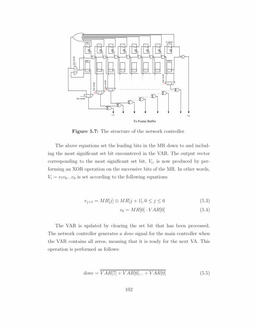
1
0
1 0
1 0
1 0
1 0
MR[7] MR[0]
VAR[0]VAR[7]
To Frame Buffer
1st c
ycle
1st cycle
1st c
ycle
1st c
ycle 1s
t cyc
le
R R R R R R R R
QQQ QQ QQD D D D D D D D
QQQQQQQQ
v7 v0
Q Q Q Q Q Q Q Q
Q
Figure 5.7: The structure of the network controller.
The above equations set the leading bits in the MR down to and includ-
ing the most significant set bit encountered in the VAR. The output vector
corresponding to the most significant set bit, Vi, is now produced by per-
forming an XOR operation on the successive bits of the MR. In other words,
Vi = v7v6...v0 is set according to the following equations:
vj+1 = MR[j] ⊕ MR[j + 1], 0 ≤ j ≤ 6 (5.3)
v0 = MR[0] · V AR[0] (5.4)
The VAR is updated by clearing the set bit that has been processed.
The network controller generates a done signal for the main controller when
the VAR contains all zeros, meaning that it is ready for the next VA. This
operation is performed as follows:
done = V AR[7] + V AR[6]... + V AR[0] (5.5)
102

Figure 5.7 shows a schematic of the network controller (NB: the logic to
initiate the MR, to control muxes and, to generate the done signal is not
shown for simplicity). The critical delay of the circuit can be derived as
follows. Assume that each multiplexor in the figure takes two 2-input gate
delays. MR[7] will require three levels of 2-input gates (the large OR gate),
two levels for the multiplexor followed by seven gate delays to update MR6
to MR0. Each vi is updated in three gate delays. Thus, the critical path of
the circuit is fifteen 2-input gate delays. It is expected that the operation of
producing each Vi word can be accomplished in a single cycle with current
and foreseeable process technologies.
5.3.3 Analysis
Area
The main component that is added to the existing Virtex design is the vector
address decoder. This system was specified in Verilog and Synopsys Design
Compiler [109] was used to map it to the TSMC 90nm cell library [118]. The
total area was found to be approximately 723 μm2. The configuration state
machine required approximately 2,174 μm2. This is insignificant compared
to the Virtex die area which is in the order of 106μm2 [123].
Time
The critical delay of the VAD was found to be approximately 14ns and can
thus be easily accommodated at Virtex configuration frequency (66MHz).
This means that the design can operate at the same speed at which configu-
ration data is input. Thus, the proposed design directly translates a decrease
in the amount of configuration data, which is made possible by fine-grained
partial reconfiguration, into a decrease in the time needed to reconfigure the
device.
103

Power
The dynamic power of the VAD was estimated to be around 228μW while
the leakage power was around 114μW . However, the dynamic power of the
memory array is expected to increase by more than a factor of two. This
is due to an increased switching overhead of the read-modify-write method.
A precise calculation of this figure involves a detailed VLSI level analysis
of large SRAM memories and is beyond the scope of this thesis (the school
did not have appropriate cell libraries for this task). ARCH-II attempts to
overcome this limitation by focusing on a write-only method and is discussed
in Section 5.4.
Limitations
There are two limitations of ARCH-I.
• A read-modify-write technique works only if the user knows the current
state of the configuration memory. A complete configuration must be
supplied when this is not the case.
• Dynamic power is increased due to a read-modify-write strategy.
• As was discussed in Chapter 4, the major source of inter-configuration
redundancy is null data. It was argued that if the device can automat-
ically reset the configuration memory to its default state then there
would be no need to add null data to clear the remains of the previous
circuits as is required in ARCH-I. In other words, ARCH-I delegates
the management of null data to the user.
These limitations can be overcome by ARCH-II which is presented in the
next section.
104
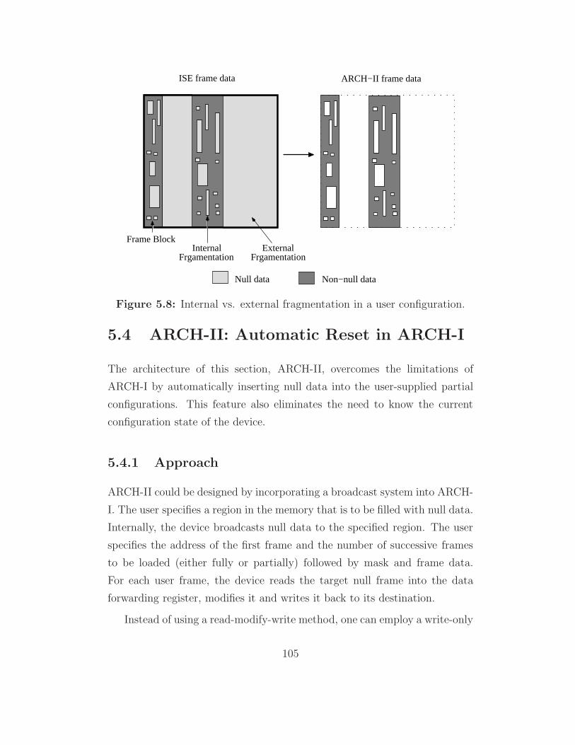
Null data Non−null data
External Frgamentation
Frame Block
FrgamentationInternal
ISE frame data ARCH−II frame data
Figure 5.8: Internal vs. external fragmentation in a user configuration.
5.4 ARCH-II: Automatic Reset in ARCH-I
The architecture of this section, ARCH-II, overcomes the limitations of
ARCH-I by automatically inserting null data into the user-supplied partial
configurations. This feature also eliminates the need to know the current
configuration state of the device.
5.4.1 Approach
ARCH-II could be designed by incorporating a broadcast system into ARCH-
I. The user specifies a region in the memory that is to be filled with null data.
Internally, the device broadcasts null data to the specified region. The user
specifies the address of the first frame and the number of successive frames
to be loaded (either fully or partially) followed by mask and frame data.
For each user frame, the device reads the target null frame into the data
forwarding register, modifies it and writes it back to its destination.
Instead of using a read-modify-write method, one can employ a write-only
105

method to save the power in the chip-wide wires. The model presented in
[92] uses a wildcarding mechanism to broadcast null data across a row of the
memory cells. This is followed by any byte updates in that row if required.
This bytes that are to be modified are addressed using VA. Once a entire
row of the cells is processed, the next row is considered and so on. The main
issue with the broadcast model is that it results in a large capacitive load.
This arises because a large number of SRAM cells need to be driven by a
single wire.
An alternative method is to separately handle the internal and external
fragmentation of configuration data. Consider a complete configuration as
generated by the ISE tools (Figure 5.8). The null data can be scattered
inside the frames or it can span entire frames which can be referred to as
internal and external fragmentation respectively. Let the process that han-
dles internal fragmentation be called Puser and the one that handles external
fragmentation, Pnull. The user specifies the frames that are to be partially
loaded and the frames that are to be completely loaded with null data. Puser
converts the partial frames into full frames by inserting null data where re-
quired. When a frame is completed, it is sent to the memory array using the
existing mechanism (i.e. via the data forwarding register). While Puser is
constructing user frames, Pnull generates null frames in the background and
sends them to the memory array. In case both processes attempt to access
the array simultaneously, we give priority to Puser. If Puser finishes before
Pnull then we simply wait until Pnull is done. This model is the basis for
ARCH-II which is described below in detail.
5.4.2 Design description
Let a user frame be a frame in which there is at least a single byte to be
updated and let a user block be a contiguous set of user frames. Similarly,
let a null block be a contiguous set of null frames. A block, user or null, is
specified by the address of the first frame, followed by the number of frames
106

in the block. The frame address/count pair will be referred to as a block
address. An ARCH-II configuration C consists of an alternating sequence
of user and null blocks. Each block may range in size from 1 to 48c frames
where c is the number of columns in the FPGA. A user loads an ARCH-II
configuration by first supplying the number of blocks in the sequence and the
type of the leftmost block. The blocks are then processed in pairs such that
for each pair of blocks, the null block address and size are used to generate
null frames in parallel with loading the partial frame data and associated
vector addresses for the user block.
The new memory needs to perform two operations in parallel. It needs
to convert the incoming partial frames into full frames and at the same time
generate null frames and load them onto the array. In both cases, null data
needs to be generated. ARCH-II achieves these operations by incorporating a
null frame handling system into ARCH-I as shown at the bottom and centre
of Figure 5.9. This system consists of a null frame generator, a null frame
register and address registers for the user and null block addresses.
The null frame register is added between the data forwarding register and
the intermediate register. The size of the null frame register is f bytes and its
inputs come from the null frame generator. The null frame generator takes
in a frame address and outputs the corresponding frame to be held in the
null frame register. The resulting null frame can be either modified by the
user supplied data or it can be shifted directly into the array (to load null
blocks).
The configuration state machine manages two block addresses; one for the
user frames and the other for the null frames. The user frame address register
is initialised with the user block address and the user block size. This address
is incremented every time a user frame is loaded into the array. When the last
done signal is generated by the VAD indicating that the current frame is ready
to be loaded, the state machine selects the user frame address register as an
input to the null frame generator which outputs the required null frame in
the null frame register. The null frame register is then selectively overwritten
107

Frame Bit Frame BitIndex Contents Index Contents
0 111110000000001111 1 1011100000000010112 001100000000001011 3 1011000000000010114 101100000000001111 5 1111000000000011116 101100000000001111 7 1011000000000010118 001100000000001011 9 011110000000001011
10 001100000000001111 11 11110000000000111112 101100000000001111 13 01110000000000101114 011110000000001011 15 00110000000000101116 101000000000001111 17 10000000000000111118 100100000000001111 19 10010000000000101120 100100000000001011 21 00010000000000101122 100000000000001111 23 10010000000000111124 100100000000001111 25 10000000000000101126 000100000000001011 27 10010000000000101128 100100000000001111 29 10010000000000111130 100000000000001111 31 10100000000000101132 001100000000001011 33 01110000000000101134 011110000000001111 35 10110000000000111136 111110000000001111 37 01110000000000101138 011100000000001011 39 00110000000000101140 101100000000001111 41 10110000000000111142 111100000000001111 43 10110000000000101144 101100000000001011 45 00110000000000101146 101100000000001111 47 111100000000001111
Table 5.1: The contents of CLB null frames.
by the contents of the FDRI and finally shifted to the memory array. When
this process completes, the null frame address register is selected for input
to the null frame generator. Null frames are produced and transferred to
the intermediate register. The state machine asserts a ready signal when all
blocks have been loaded.
The null frame generator is designed by examining the structure of Vir-
tex’ null configuration using JBits. The following discussion focuses only on
the CLB-type frames as they form the majority of configuration data. It
108
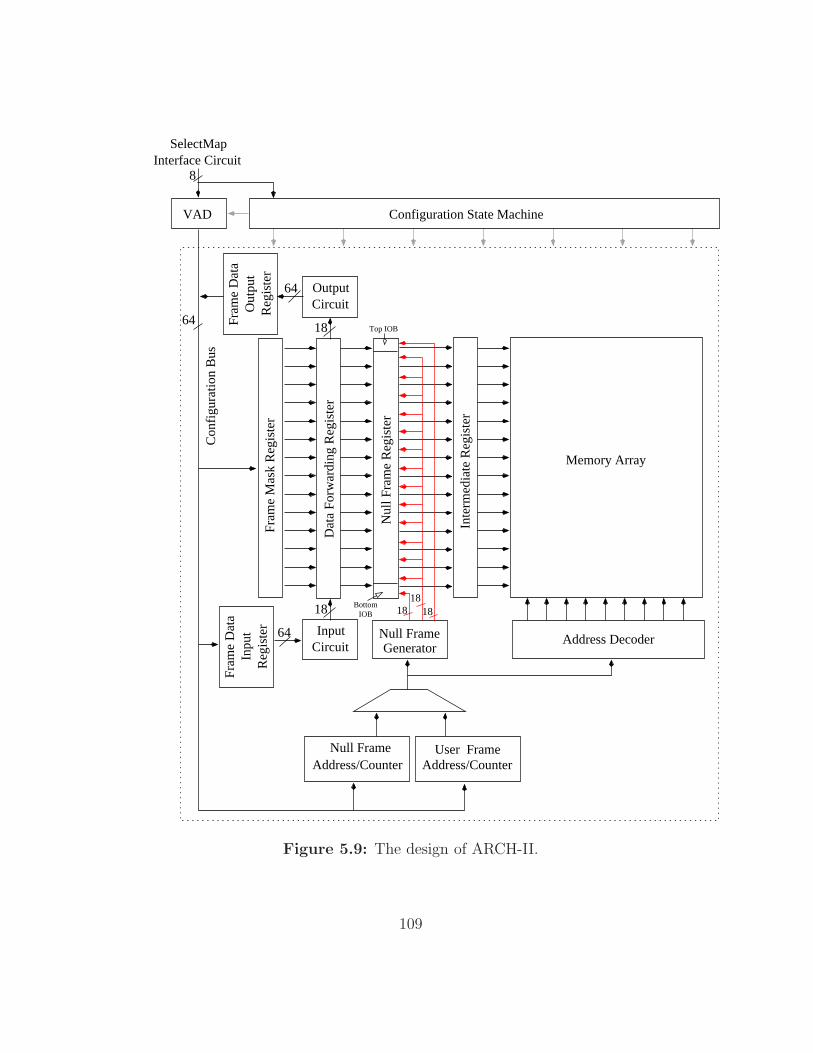
Address/CounterUser Frame
InputCircuit
Fram
e D
ata
Reg
iste
rIn
put
Nul
l Fra
me
Reg
iste
r
Inte
rmed
iate
Reg
iste
r
Address Decoder
Memory Array
Null FrameGenerator
Address/CounterNull Frame
Fram
e M
ask
Reg
iste
r
Con
figu
ratio
n B
usConfiguration State Machine
CircuitReg
iste
r
Output
Out
put
Fram
e D
ata
Dat
a Fo
rwar
ding
Reg
iste
r
VAD
Interface CircuitSelectMap
8
64
64
18
18
64
18 1818
Top IOB
BottomIOB
Figure 5.9: The design of ARCH-II.
109

was found that CLB-type frames at the same indices in each column were
identical. Moreover, within each frame, the 18 bits corresponding to a CLB
target identical resources in each CLB. This is also the case for the top and
bottom IOB bits. An 18× 48 bit block is therefore sufficient to describe the
null bits of each CLB. It should be noted that in Virtex these null bits are
not all zero. One can design the FPGA fabric such that there is an automatic
reset akin to resets in conventional SRAMs thereby eliminating the need for
the null frame generator. As the VLSI circuit level details of Virtex are not
public, and the power required to simultaneously reset large regions of the
configuration memory is likely to be excessive, an implementation of the null
frame generator is preferred.
One method for implementing the null frame generator is simply to store
18×48 bits of null data in a memory addressed by the frame indices. However,
further examination of the null bits within a CLB reveals regularities that
can be exploited to reduce the area requirements of the null frame generator
for Virtex.
Table 5.1 shows the contents of the null bits for a Virtex CLB. By inspec-
tion, it is possible to observe that these data are highly regular and therefore
can be significantly compressed. The first observation is that the middle nine
bits in each 18-bit fragment are always zero. The first five bits are in the set:
first = {11111, 00110, 10110, 01111, 10100, 10010, 10000, 10010,
00010, 01100, 11110, 10111, 01110, 10010, 00010} while the last four in are in
the set: last = {1111, 1011}. Thus, any 18-bit fragment can be represented
as a concatenation of three bit segments. The first segment is five bits long
and belongs to first followed by nine zeroes, followed by a 4-bit segment from
last. There are 15 elements in first and two elements in last. Thus, 5 bits
are enough to represent each 18-bit fragment. A small ROM or PLA can be
used to implement the required mapping between the frame indices and one
of the eighteen possible output values. It is expected that this system will
generate an entire null frame within a single cycle. The 18 bits for nulling
the CLB contents are broadcast to all CLBs spanned by the frame while the
110

top and bottom IOB are nulled using their specific 18-bit codes.
5.4.3 Analysis
ARCH-II adds a null frame handling system to ARCH-I. This circuit is simple
and adds little to the chip area. ARCH-II generates a null frame within one
clock cycle. The generated frame is transfered to the array in the next cycle
while a new null frame is being generated. Thus, the null frame generator
maintains a constant throughput of one frame per cycle. ARCH-II resets
the entire memory array in 48c cycles where c is the number of columns
in the target device. Suppose there are i null frames to be loaded, where
0 ≤ i ≤ 48c. If i exceeds the number of bytes in the input user configuration
(configuration data + frame address overheads) then we have to wait until
all null frames have been loaded. For practical purposes, this wait time will
be zero as the data presented in Chapter 4 shows that even small circuit
cores contain several thousand bytes of configuration data. Moreover, if the
user knows the current state of the configuration memory then the on-chip
null frames need not be re-generated. In principle, the bitstream structure
can take into account null block sizes and the delays of the configuration
system architecture in order to insert null block addresses into the user data
wherever convenient. Strict interleaving of user and null block loads is not
necessary; wait times can thus be minimised.
Table 5.2 compares the performance of ARCH-II with Virtex. Results are
shown for three different device sizes and each column shows the percentage
reduction in the amount of configuration data as compared with Virtex’
frame-oriented partial reconfiguration. Comparing Table 5.2 with Tables
4.10 to 4.12), it can be seen that the frame-oriented VA performs better than
the device-level VA for small circuits because only those frames are updated
that contain some non-null data and no VA is supplied for the frames that are
entirely null. As the circuit size is increased, the frame-level VA performs
slightly worse than the device-level VA because of the extra padding that
111

Circuit % ReductionXCV200 XCV400 XCV1000
encoder 82 84 85uart 62 63 57asyn-fifo 70 68 62add-sub - 68 642compl-1 - 69 65spi 64 60 55fir-srg 49 50 56dfir 64 64 55cic3r32 63 57 30ccmul 63 57 48bin-decod - 72 722compl-2 - 72 69ammod 60 66 67bfproc 60 71 71costLUT 59 65 35gpio 63 65 68irr 62 58 56des - 66 73cordic 57 57 62rsa 54 60 63dct 55 63 57blue-th - 59 68vfft1024 - 56 60fpu - 48 61
Mean 62 63 61
Table 5.2: Percentage reduction in reconfiguration time of ARCH-II com-pared to current Virtex.
112

is needed to make the frame an integral multiple of the required block size.
Thus, the combination of RAM with VA provides a good overall compromise.
5.5 ARCH-III: Scaling Configuration Port
Width in ARCH-II
The parameters of the proposed vector address decoders in ARCH-I and
ARCH-II were determined by the size of the configuration port. For example,
8 bytes are processed by the VAD in each architecture because the port is 8
bits wide. This section discusses the issue of scaling the configuration port
width. It examines various methods for parallelising the operation of ARCH-
II so that the presence of a large port results in a proportionate reduction
in the reconfiguration time. These methods result in ARCH-III, a scalable
memory that supports fine-grained partial reconfiguration in Virtex.
5.5.1 Approach
Let us suppose that the configuration port size in ARCH-II is increased from
8 bits to 8p bits where p > 1. The VAD in ARCH-II needs to be re-designed
as it only accepts data on a byte-by-byte basis. One strategy would be
to implement an 8p-bit wide VAD and a 64p-bit wide configuration bus to
support the parallel load of 8p bytes. This scheme is not practical for large p
for the following reasons. Firstly, the delay through the VAD is proportional
to 8p making a single cycle operation difficult to achieve for large values of p.
Secondly, the amount of wiring demanded by the configuration bus can be
prohibitive. Therefore, a different approach is needed to handle large port
sizes.
An alternative scheme is to implement several 8-bit VAD-FDRI systems
that operate in parallel. A VAD-FDRI system is shown in Figure 5.10. It
consists of a VAD, a configuration bus, an FDRI, a mask register and a data-
113

forwarding register. The dimensions of these components are the same as in
ARCH-II. A Virtex with a configuration port of size 8p bits will contain
p VAD-FDRI systems as shown in Figure 5.11. The configuration port is
divided such that each VAD-FDRI has its own 8-bit wide port. Each VAD-
FDRI is a stand-alone system and produces a frame in its FDRI. The last
done signal from a given VAD-FDRI instructs the state machine to transfer
its current frame to the intermediate register. Each VAD-FDRI is connected
to a single data forwarding bus of size 8f bits where f is the number of bytes
in the frame. This bus transfers the contents of a VAD-FDRI system to the
intermediate register. Bus contention may arise in case where several frames
are ready simultaneously. This conflict can be resolved using a bus arbiter. A
p-bit priority decoder can be used for this purpose. The VAD-FDRI systems
waiting for their frames to be transfered over the data forwarding bus cannot
accept more data from their input port.
The main advantage of this method is that the vector decoding delay is
indepedant of the port size. The main disadvantage is that each VAD con-
tains its own 64-bit wide configuration bus. The aggregate bus size therefore
scales with p. This limitation can be avoided by implementing a fixed sized
configuration-bus that is shared among all vector address decoders. This
forms the basis for ARCH-III.
5.5.2 Design description
The common configuration-bus architecture is shown in Figure 5.12. The
VAD-FDRI systems, as discussed above, are split about the configuration
bus as shown. Each VAD has its own 8-bit wide configuration port and its
own frame address register (FAR). A single configuration bus, of size 64-bits,
is used to transfer data between various components. A bus arbiter resolves
the conflicts if more than one component attempts to access the bus at a
time.
In the new system, the 8p wide configuration port is equally divided
114

InputCircuit
64
64
18
Fram
e D
ata
Inpu
t R
egis
ter
Con
figu
ratio
n B
us
Fram
e M
ask
Reg
iste
r
VADSystem
Configuration state machine
Dat
a Fo
rwar
ding
Reg
iste
r
Nul
l Fra
me
Reg
iste
r
From Null frame generator
Dat
a fo
rwar
ding
bus
18
18
18
Figure 5.10: The VAD-FDRI System.
115

88
BusArbiter
8
Null framegenerator
Configuration State Machine
Interface Circuit
8p
Nul
l Fra
me
Reg
iste
r
Inte
rmed
iate
Reg
iste
r
Mem
ory
Arr
ay
VA
D−
FDR
I Sy
stem
−1
VA
D−
FDR
I Sy
stem
−2
VA
D−
FDR
I Sy
stem
−p
data forwardingShared
bus
8f
Figure 5.11: The parallel configuration system.
116

System pVAD−
8 8 8
System 2VAD−
Null framegenerator
Shared dataforwarding bus
BusArbiter
System−1VAD−
System 2
Configuration State Machine
8pInterface Circuit
Inte
rmed
iate
Reg
iste
r
Mem
ory
Arr
ay
Nul
l Fra
me
Reg
iste
r
FDRI− FDRI−System p
64
FDRI−System 1
BusArbiter
54
Sharded nullframe bus
Sharedconfiguration bus
8f
Figure 5.12: The datapath of ARCH-III.
117

among p VADs. From the user’s perspective, each VAD is provided with a
user block address followed by the mask and frame data, in the same manner
as ARCH-II. If the the number of user blocks is not a multiple of p than
the user can split them evenly among the p decoders. Each VAD performs
its operation independently. Consider the ith VAD where 1 ≤ i ≤ p. For
each byte of VA processed, it generates a done signal. This signals the
state machine that in the next cycle the frame buffer of this VAD is to be
shifted to the ith FDRI, via the configuration bus (C-Bus). The VAD sends
a bus request to the configuration-bus arbiter. As more than one VAD can
send a request signal at a time, the bus arbiter decides which one will be the
bus master.
Each VAD needs to transfer not only its frame bytes but also the corre-
sponding mask bytes. Since the configuration bus is set to 64 bits wide, it
will take each VAD two cycles to send this data. Instead of increasing the
width of the C-bus, the method presented here transfers VA bytes and the
mask from a particular VAD in two successive cycles. In other words, the
bus arbiter allocates the bus to a VAD for two successive cycles.
Various schemes can be used to implement the operation of the arbiter.
A simple method would be to assign a number between 0 and p−1 and give a
higher priority to the higher numbered VAD. Once an entire frame is loaded
in the ith FDRI, it is transfered to the null frame system. The bottom bus
arbiter performs this arbitration. A priority decoder can be used to decide
between various FDRI systems.
The VADs that cannot access the bus in a given cycle will need to wait
until the arbiter decides to give them the bus. These VADs will not be
able to process more VA bytes. Any input data during this wait state will
be discarded by a VAD. Thus, the user needs to insert pad bytes into the
configuration data.
Once a frame in the ith FDRI is ready to be transfered, the data forward-
ing bus (DF-Bus) is required. Notice that there can never by any conflict
118

over the DF-Bus. This is because only one VAD can access the C-Bus at any
time. Therefore, only one VAD can finish loading its frame during a given
cycle. In the next cycle, this loaded frame will be forwarded to the array
thereby freeing the DF-Bus for use by some other VAD. The overall control
of each V AD is shown in Figure 5.13.
ARCH-III can also internally generate null frames and load them into
a user-specified region of the memory. This step is performed in the same
manner as in ARCH-II. The configuration state machine is instructed with
the null-block addresses through a dedicated part of the configuration port.
The scheduling of the null frames is the same as in ARCH-II. Notice that a
separate null frame register is required for this operation.
5.5.3 Analysis
This section evaluates the overhead of inserting pad data into the original
configuration bitstream to account for wait states that arise when multiple
FAD systems contend for the C-bus as the port size is increased. The bench-
mark circuits from Chapter 4 were considered for an XCV400 device. The
null bytes in each configuration were removed. The operation of ARCH-III
was simulated for various values of p. Each VAD was assigned a unique
number and a higher priority was given to lower numbers. The amount of
dummy data needed for each circuit was determined by counting the number
of times each VAD was stalled. Details of this simulation are provided in
Appendix C.
Ideally, reconfiguration time should decrease by a factor of p as p is in-
creased. For example, for p = 2, the reconfiguration time should be half
that of p = 1. Figure 5.15 reports the fraction by which ARCH-III reduces
the reconfiguration time as p is scaled. This graph is obtained by simulating
the operation of ARCH-III assuming an XCV400 device. The benchmark
circuits were considered and the mean finish time was calculated. This was
then compared to the mean time for p = 1 (i.e. ARCH-II). Details of the
119
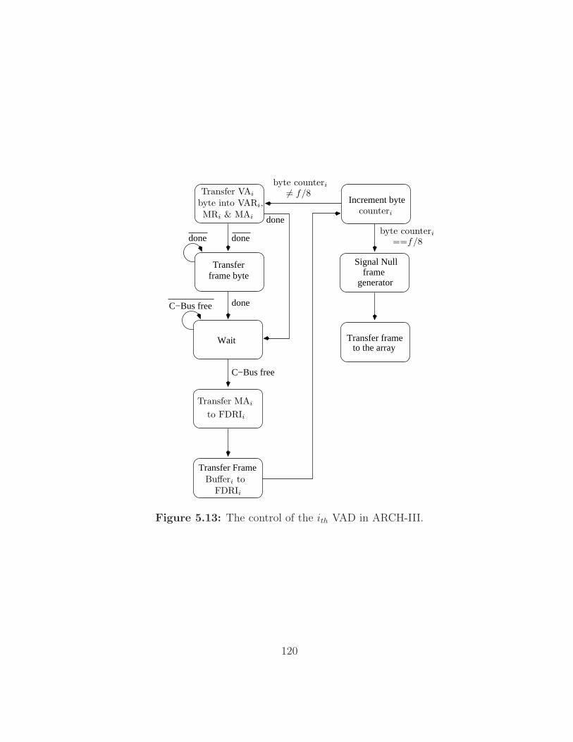
done
Transfer frame byte
done
C−Bus free
Transfer frameto the array
done
Wait
C−Bus free
Transfer Frame
done
Signal Nullframe
generator
Increment byte byte into VARi,Transfer VAi
Transfer MAi
byte counteri
counteri
to FDRIi
MRi & MAi
�= f/8
byte counteri
==f/8
Bufferi toFDRIi
Figure 5.13: The control of the ith VAD in ARCH-III.
120
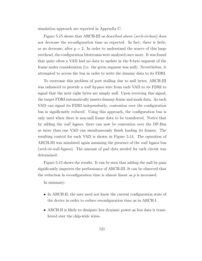
simulation approach are reported in Appendix C.
Figure 5.15 shows that ARCH-III as described above (arch-iii-base) does
not decrease the reconfiguration time as expected. In fact, there is little,
or no decrease, after p = 2. In order to understand the source of this large
overhead, the configuration bitstreams were analysed once more. It was found
that quite often a VAD had no data to update in the 8-byte segment of the
frame under consideration (i.e. the given segment was null). Nevertheless, it
attempted to access the bus in order to write the dummy data to its FDRI.
To overcome this problem of port stalling due to null bytes, ARCH-III
was enhanced to provide a null by-pass wire from each VAD to its FDRI to
signal that the next eight bytes are simply null. Upon receiving this signal,
the target FDRI automatically inserts dummy frame and mask data. As each
VAD can signal its FDRI independently, contention over the configuration
bus is significantly reduced. Using this approach, the configuration bus is
only used when there is non-null frame data to be transferred. Notice that
by adding the null bypass, there can now be contention over the DF-Bus
as more than one VAD can simultaneously finish loading its frames. The
resulting control for each VAD is shown in Figure 5.14. The operation of
ARCH-III was simulated again assuming the presence of the null bypass bus
(arch-iii-null-bypass). The amount of pad data needed for each circuit was
determined.
Figure 5.15 shows the results. It can be seen that adding the null by-pass
significantly improves the performance of ARCH-III. It can be observed that
the reduction in reconfiguration time is almost linear as p is increased.
In summary:
• In ARCH-II, the user need not know the current configuration state of
the device in order to reduce reconfiguration time as in ARCH-I.
• ARCH-II is likely to dissipate less dynamic power as less data is trans-
ferred over the chip-wide wires.
121

done
Transfer frame byte
done
Transfer frameto the array
done
Wait
C−Bus free
Transfer Frame
done
Signal Nullframe
generator
Increment byte
Wait
DF−Bus freeC−Bus free
Signal Null bypass to byte into VARi,
Transfer VAi
Transfer MAi
to FDRIi
MRi & MAi
Bufferi toFDRIi
byte counteri
counteri
byte counteri
FDRIi
�= f/8
==f/8
Figure 5.14: The control of the ith VAD in ARCH-III with the null bypass.
122

0
0.1
0.2
0.3
0.4
0.5
0.6
0.7
0.8
0.9
1
2 4 6 8 10 12 14 16
Per
form
ance
of A
RC
H-I
II w
.r.t.
p=
1
Port size p (bytes)
"arch-iii-ideal""arch-iii-base"
"arch-iii-null-bypass"
Figure 5.15: Evaluating the performance of ARCH-III. Target device =XCV400.
123
• ARCH-II automatically inserts null data in the user supplied bitstream
thereby further reducing the reconfiguration time compared to ARCH-I
(see the analysis of Section 4.5).
• ARCH-III can be scaled with respect to the configuration port size.
The architectures presented in this chapter have ignored the existence
of such artifacts in contemporary FPGAs as Block RAMs (or other embed-
ded structures such as multipliers). While BRAM configuration is not that
significant in quantity, it might become so in the future given the ever in-
creasing transistor density. BRAM configuration can be classified as consist-
ing of BRAM content configuration and BRAM interconnect configuration.
The analysis of this thesis suggests that significant sparsity is expected in
the BRAM interconnect configuration. BRAM content configuration, on the
other hand, is likely to be more application specific and hence further analysis
is needed to characterise its compression.
5.6 Conclusions
This chapter has presented new configuration memory architectures to en-
hance the current Virtex so as to increase its reconfiguration speed. This was
achieved by introducing two new features, byte-level partial reconfiguration
and automatic reset of the configuration memory, into the current device. It
was shown that the new architectural features could be scaled with configura-
tion port size and that they demand negligible additional hardware resources
for their operation. The next chapter explores the benefits of compressing
configuration data and enhances the architectures presented in this chapter
to further reduce the reconfiguration time.
124

Chapter 6
Compressing Virtex
Configuration Data
6.1 Introduction
The analysis presented in Chapter 4 suggests that it is more useful to repre-
sent a circuit’s configuration as a null configuration together with an edit-list
of the changes made by the circuit. From the perspective of compressing con-
figuration data, one can simply hard-code the null configuration for a device
in the decompressor and supply it the list of changes needed to implement
the input circuit. The analysis in Chapter 4 investigated various address en-
coding techniques, such as binary encoding, runlength encoding and unary
encoding to represent the locations of the changes in the null configuration
made by the input circuit. This chapter investigates the problem of encoding
configuration data from the broader perspective of compression. The results
of this chapter are published in [62].
Techniques for configuration compression are actively studied in the area
of field programmable logic. There are two motivations behind such meth-
ods. As FPGAs become larger their configuration bitstream sizes increase
proportionately. Compression is seen as a suitable mechanism to reduce
125

storage requirements especially if the device is to boot from an embedded
memory. The other motivation behind configuration compression is to re-
duce reconfiguration time for a circuit. The main difference between the two
approaches is that the time to decompress and load configuration data is
not critical in the first case whereas it is an important factor in the second
(please see Section 2.3 for a discussion).
Several researchers have investigated configuration compression showing
20%-95% reduction in configuration data for various benchmark circuits.
However, it is not clear how the various compression techniques can be com-
pared. Indeed, what are the limits of configuration compression? Moreover,
what parameters of circuits and devices impact upon the performance of
these techniques?
To address the above issues, this chapter first proposes an objective mea-
sure of how well a given configuration bitstream can be compressed. Section
6.2 defines the entropy of reconfiguration to be the entropy of the config-
uration bitstream that is required to configure a given input circuit. The
entropy is defined in terms of the probability of finding various symbols in
the configuration data. In order to estimate these probabilities, a model of
configuration data is then presented which is based on a detailed empirical
analysis of the chosen set of benchmark configurations for Virtex devices. In
the light of this model, the entropies of various circuit configurations are then
computed. It is shown that for the benchmark circuits, the entropy remains
almost constant irrespective of the circuit or the device sizes.
Section 6.3 presents an analysis of the existing approaches towards con-
figuration compression. It is argued that these methods not only require
complex operations but also exhibit relatively poor compression. In the light
of this discussion, Section 6.4 then empirically evaluates two simple alter-
native compression techniques: Golomb encoding and hierarchical vector
compression. These techniques are selected in the light of the model pre-
sented in Section 6.2. It is shown that these methods perform within 1-10%
of the best possible compression. Vector compression is chosen for hardware
126
implementation due to its simplicity.
Section 6.5 studies the issues related to hardware implementation of a vec-
tor decompressor. A scalable hardware decompression system, ARCH-IV, is
presented and analysed in detail. It is shown that this system translates a
decrease in configuration size, made possible by compression, into a propor-
tionate decrease in reconfiguration time.
6.2 Entropy of Reconfiguration
In order to gain an insight into the performance of various compression tech-
niques and to cross-compare results, this section outlines an approach derived
from the basic results of information theory. Let us consider the FPGA recon-
figuration as a communication problem whereby configuration information is
transfered to the device via the configuration port (which can be thought
of as the channel). Given this viewpoint, one can attempt to measure the
information content of typical FPGA reconfiguration. This will give us a the-
oretical bound on the compression against which the performance of various
encoding schemes can be measured.
More precisely, we are interested in finding the minimum amount of con-
figuration data needed to configure a given circuit on a given device. Con-
sidering a circuit configuration as a bit string, we are interested in finding
the length of the shortest string representing that configuration, i.e. its Kol-
mogorov complexity. However, finding the Kolmogorov complexity of an
arbitrary string is NP hard. This chapter, therefore, follows the approach
commonly used in the field of text compression [79]. If one can model the
data source, i.e. can determine the probabilities of various symbols it out-
puts, then one can easily determine its entropy, which provides a bound on
compressibility. This is what the subsequent sections aim to show.
127

6.2.1 Definition
Let us recall the definition of entropy (also called Shannon’s entropy ). Let
X be a discrete random variable defined over a finite set of symbols. Let the
probability distribution function of X be p(x) = Pr(X = x). The entropy,
H(X), can be defined as [83]:
H(X) = −∑
x∈X
p(x)log2(p(x)) (6.1)
The entropy of a memoryless information source determines the minimum
channel capacity that is needed for a reliable transmission of the source.
In other words, entropy provides an estimate of the minimum number of
bits that are needed to encode a string of symbols produced by the source.
Encoding a message with less than H(X) bits per symbol will result in a loss
of information (or the communication will be unreliable).
Consider an FPGA that is in an unknown configuration state and a new
circuit that is to be configured onto the device. The entropy of reconfigura-
tion, Hr, can be defined to be the entropy of the data source that generates
the configuration bitstream required to configure the input circuit onto the
target FPGA. The interpretation of Hr is that it defines the minimum num-
ber of bits/symbol needed to configure the required circuit and therefore
provides an estimate of the maximum compression possible for the configu-
ration. Application of this method presupposes that FPGA configurations
can be modelled as strings of randomly generated symbols without significant
error. One is therefore charged with finding suitable symbol sets and evalu-
ating a representative set of configurations to determine the validity of the
randomness assumption. Assuming this can be done, it is therefore possible
to assess the performance of given compression heuristics and obtain lower
bounds on the delay involved in configuring the circuit.
128

6.2.2 A model of Virtex configurations
Let us formalise the notion of a list of changes that a circuit makes to a null
configuration. A φ′ configuration of a given configuration, C, is simply a
vector that specifies the bits in C that are different from the corresponding
bit in the null configuration. As the null configuration for Virtex devices
does not entirely consist of zeros, let us define φ′ as follows. Let there be a
null configuration, φ, represented as a bit vector of size n bits. Let there be
a circuit configuration C also of size n bits. Let k be the number of bits in
C that differ from the corresponding bit in φ. A new bit vector, φ′, of size
n bits is constructed as follows. All bits in φ that remain unchanged in C
are left unset while the rest are set to one. Thus, φ′ contains exactly k ones.
In other words, φ′ represents the positions in φ where the bits need to be
flipped in order to configure the input circuit. The problem of compressing
configuration data can be transformed into a problem of compressing the
φ′ configuration of an input configuration. This is an incarnation of the
configuration addressing problem defined in Section 4.7.
The aim of the model is to define a suitable symbol set over φ′ and to
assign probability distributions to these. The most striking feature of the φ′
vectors is their sparsity, i.e. long runs of zeros. Given this observation, let
us consider the runlengths of zeros as our symbol set. Let X be a random
variable that specifies this runlength where X ∈ {0, 1, 2, ...., n− 1}. In other
words, X = i means that the output symbol contains i zeros followed by a
one. In the following discussion, a run of length i bits means i zeros followed
by a one. The problem of finding a probability distribution function for the
model data source can thus be formulated as finding a probability distribution
of X.
One could consider alternative symbol sets, such as fixed length binary
codes, to model the configuration data as long as one can satisfy the ran-
domness assumption of the entropy equation. However, if one can model a
random data source using a particular symbol set, S, then any other model
129

Circuit XCV200 XCV400 XCV1000k Hr Shan. k Hr Shan. k Hr Shan.
(bits) %red. (bits) %red. (bits) %red.encoder 4,302 5.48 98 4,394 5.36 99 4,320 5.28 99uart 5,321 5.39 98 5,129 5.10 99 5,536 5.15 99asyn-fifo 5,441 6.00 97 5,885 5.69 99 5,913 5.69 99add-sub - - - 5,997 6.59 98 6,155 5.84 992compl-1 - - - 7,806 6.50 98 9,212 6.18 99spi 7,983 5.60 96 7,956 5.63 98 8,041 4.93 99fir-srg 8,534 4.93 96 8,503 4.92 98 8,169 4.72 99dfir 7,981 5.30 96 8,535 5.09 98 8,710 4.91 99cic3r32 9,061 5.00 96 9,092 4.88 98 8,478 4.79 99ccmul 9,956 5.67 95 9,956 5.66 98 10,215 5.55 99bin-decod - - - 10,670 7.33 97 10,648 6.66 992compl-2 - - - 11,154 6.75 97 12,738 6.61 99ammod 11,546 5.21 95 11,653 5.24 97 12,032 5.27 99bfproc 14,753 5.04 94 14,859 5.16 97 15,497 5.34 99costLUT 16,424 5.54 92 16,752 5.76 96 16,093 5.13 99gpio 30,762 5.35 86 30,924 5.56 93 32,226 5.92 97irr 34,830 4.81 86 33,648 4.68 93 33,506 4.67 97des - - - 48,118 5.23 89 49,827 5.88 95cordic 48,759 4.71 80 49,364 4.63 90 50,202 4.70 96rsa 49,179 4.78 80 50,121 5.00 89 51,283 5.10 95dct 52,916 4.84 78 52,999 4.93 89 53,959 5.08 95blue-th - - - 100,996 4.90 79 101,776 5.39 90vfft1024 - - - 113,695 4.53 78 114,648 4.75 91fpu - - - 155,387 4.66 69 155,354 5.01 86
Table 6.1: Predicted and observed reductions in each φ′ configuration.
130

that uses a different symbol set, S ′, such that each symbol from S ′ can be
formed from S by simple concatenations yields the same entropy value. The
symbol set that uses runlengths therefore covers a broad symbol space.
To find a probability distribution function for the benchmark φ′ config-
urations, the frequency with which runs of various lengths occur in the test
data is considered. Let f(i) be the number of times a run of length i bits
occurs in a given φ′. Without loss of generality let us assume that the first
and the last bits in φ′ are zeros. With this assumption, the total number of
runlengths in φ′ is k + 1. Thus, the probability that a run of length i bits
occurs in φ′ is given by f(i)k+1
. The benchmark φ′ configurations for various
devices were examined. For each benchmark configuration, the frequencies
of the shortest few thousand runlengths were determined.
The results are illustrated by considering the φ′ for four selected circuits
on an XCV400. It was found that P (X = 0) was approximately 0.25 for each
case. The remaining run-lengths are distributed as illustrated in Figure 6.1.
The other φ′ configurations in the benchmark exhibit a similar trend.
6.2.3 Measuring Entropy of Reconfiguration
The entropy of reconfiguration for each benchmark circuit, represented as a φ′
vector, was thus calculated using Equation 6.1 with runlengths of zeros as the
symbol set. Results corresponding to circuits mapped onto various devices
are recorded in Table 6.1 under the columns headed Hr. The minimum
bitstream size for a circuit is estimated by k × Hr. Thus, the estimated
minimum number of bits needed to encode the fpu φ′ for an XCV400 is
155, 387 × 4.66 = 724, 103, which is 31.4% of the size of the complete CLB
configuration for an XCV400 (n = 2,304,000). In other words, the best
compression possible for this circuit configuration is 68.6% (Table 6.1 column
Shann. % red.). The figures are rounded due to uncertainty in the results as
indicated. The table is sorted in an increasing order of k.
131

0
0.01
0.02
0.03
0.04
0.05
0.06
0.07
0.08
0 10 20 30 40 50 60 70 80 90 100
Pro
babi
lity
of X
=i
Run size in bits (X=i)
"fpu_xcv400"
(a) Circuit fpuxcv400
0
0.01
0.02
0.03
0.04
0.05
0.06
0.07
0.08
0 10 20 30 40 50 60 70 80 90 100P
roba
bilit
y of
X=
iRun size in bits (X=i)
"des_xcv400"
(b) Circuit desxcv400
0
0.01
0.02
0.03
0.04
0.05
0.06
0.07
0.08
0 10 20 30 40 50 60 70 80 90 100
Pro
babi
lity
of X
=i
Run size in bits (X=i)
"bin_decod_xcv400"
(c) Circuit bin-decodxcv400
0
0.01
0.02
0.03
0.04
0.05
0.06
0.07
0.08
0.09
0.1
0 10 20 30 40 50 60 70 80 90 100
Pro
babi
lity
of X
=i
Run size in bits (X=i)
"2compl-1_xcv400"
(d) Circuit 2compl-1xcv400
Figure 6.1: The relationship between runsize i and P (X = i), i > 0, forfour selected circuits on an XCV400.
132
6.2.4 Exploring the randomness assumption of the
model
On the surface, the problem of establishing the randomness of the runlengths
looks similar to the problem of establishing the randomness of a random num-
ber generator (RNG) for which several methods exist (e.g. the tests used in
[64]). However, a closer analysis reveals that the tests for RNGs assume
that the generated numbers are uniformly distributed, i.e. each number has
the same probability. Figure 6.1, on the other hand, suggests an exponen-
tial distribution. However, several simple experiments can be used to show
that for practical purposes, the randomness assumption of the model is valid.
This assertion is supported by the observation that circuit flattening result-
ing from synthesis, place and route tools should result in a relatively random
use of resources and that this ought to produce a corresponding randomness
in the setting of switches as given by φ′. In the remainder of this subsec-
tion, the experiments conducted to support the hypothesis of random symbol
distribution are reported.
Experiment 1
The motivation behind this experiment is the fact that the entropy of a
random process is independent of the number of symbols already produced.
By verifying that the calculated entropy of successively shorter tails of our
benchmark configurations does not change significantly, some confidence can
be gained that runlengths (set bits) are randomly distributed throughout the
data.
The entropies H tr of all configurations having skipped the leading t sym-
bols in the φ′ bitstreams were calculated. The results for four circuits that
were mapped to an XCV400 and which are representative of the range in
complexity and size present in the benchmark set appear plotted in Figure
6.2. For these plots the H tr is calculated at increments of t = 1000. Since
the number of symbols k + 1 per configuration varies substantially for these
133
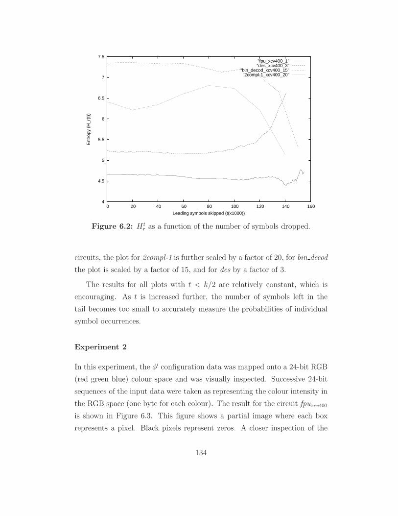
4
4.5
5
5.5
6
6.5
7
7.5
0 20 40 60 80 100 120 140 160
Ent
ropy
(H
_r(t
))
Leading symbols skipped (t(x1000))
"fpu_xcv400_1""des_xcv400_3"
"bin_decod_xcv400_15""2compl-1_xcv400_20"
Figure 6.2: H tr as a function of the number of symbols dropped.
circuits, the plot for 2compl-1 is further scaled by a factor of 20, for bin decod
the plot is scaled by a factor of 15, and for des by a factor of 3.
The results for all plots with t < k/2 are relatively constant, which is
encouraging. As t is increased further, the number of symbols left in the
tail becomes too small to accurately measure the probabilities of individual
symbol occurrences.
Experiment 2
In this experiment, the φ′ configuration data was mapped onto a 24-bit RGB
(red green blue) colour space and was visually inspected. Successive 24-bit
sequences of the input data were taken as representing the colour intensity in
the RGB space (one byte for each colour). The result for the circuit fpuxcv400
is shown in Figure 6.3. This figure shows a partial image where each box
represents a pixel. Black pixels represent zeros. A closer inspection of the
134

image reveals that the zeros are distributed in an almost random fashion and
any significant pattern is difficult to decipher.
Experiment 3
In this experiment, a Fourier transform was applied to the runlengths present
in various configurations. The Fourier transform converts a signal from the
time domain into the frequency domain. Any significant periodic behaviour
can thus be detected by inspecting the spectrum of the frequency domain sig-
nal. Figure 6.4(a) shows the power spectrum of the φ′ configuration fpuxcv400.
This spectrum can be compared to the spectrum of a random signal which
is shown in Figure 6.4(b). These figures have been produced using MAT-
LAB 7.0 [114]. From the figure, the frequency of runlengths in the input
configuration appears to be randomly distributed.
Experiment 4
This experiment combines Experiments 2 and 3. The configuration images
produced in experiment 3 were transformed into JPEG representation. JPEG
encoding internally performs a two-dimensional discrete cosine transform of
the image followed by quantisation and encoding of the coefficients. JPEG
performs lossy compression of the input image. The extent of the loss can
be traded off with the size of the resulting compressed file. Using Adobe
Photoshop 7.0 [103], the performance of JPEG was varied from the best
compression to the worst (these scales correspond to Adobe’s undisclosed
internal scale). It was found that when JPEG was in near lossless mode,
the resulting files were compressed by less than 10% and in some cases they
were larger than the original (i.e. negative compression). If there were any
significant patterns in two dimensions, the result would have been different.
In its lossy mode, JPEG reduced various input configurations by 85% but
at the cost of considerable image distortion. As it is difficult to estimate
the extent of this information loss, we are unable to provide a quantitative
135

Figure 6.3: A slice of configuration data corresponding to circuit fpuxcv400.The image is shown in 24 bits RGB colour space.
136

0 1 2 3 4 5
x 104
10−3
10−2
10−1
100
101
102
103
104
105
Frequency content of fpu−xcv400
Frequency (Hz)
Pow
er (
Wat
ts/H
z)
(a) Power spectrum of the runlengths in the fpu φ′ configura-tion.
0 1 2 3 4 5
x 104
10−5
10−4
10−3
10−2
10−1
100
101
102
Frequency (Hz)
Pow
er (
Wat
ts/H
z)
Frequency content of a random signal
(b) Power spectrum of a random signal
Figure 6.4: Comparing the power spectrums of the runlengths in the φ′ offpu configuration and a random signal.
137
analysis of JPEG’s compression for the data under test.
The results of the above experiments suggest that for practical purposes,
one can consider the set bits in an FPGA configuration data to be randomly
located and can therefore apply Shannon’s formula to measure the entropy.
6.3 Evaluating Existing Configuration Com-
pression Methods
This section analyses a well-known result that is based on the LZSS compres-
sion method [53] and a recent result that outperforms the LZSS technique
[71]. These methods are analysed in the light of the entropic model outlined
above and by considering the complexity of the hardware decompressors. It
is shown that while these methods provide a fair enough performance, the
complexity of compression and decompression highlights the need for simpler
methods.
6.3.1 LZ-based methods
The LZ algorithm
LZ-based techniques examine the input data stream during compression [79]
A dictionary of already seen data patterns is maintained. When new data
arrives, this dictionary is examined to see if the pattern in the new data
already exists in the dictionary. If it does, then an index to that pattern and
the pattern length is output, else the new pattern is added to the dictionary.
Several variations of this basic idea exist (e.g. LZ77 [101], LZ78 [102], LZSS
[89], LZW [97] . See [79] for a detailed discussion). In general, LZ78 and LZW
achieve better compression ratios but they require large dictionary sizes.
In the context of configuration compression, they are therefore considered
less suitable because large dictionary sizes imply maintaining a large on-
chip memory. On the other hand, LZ77 and its variations have attracted
138

w e r (1,5,q)
Output
b t d g f q w e r
Step 1
Step 2
a b t d g f d s e e e c d s r t g d e e f
d s e e e c d s r t g d e e f b t d g f q
Figure 6.5: An example operation of the LZ77 algorithm.
considerable attention because they require a small buffer, or sliding window,
to keep the dictionary.
The LZ77 algorithm exploits regularities between successive pieces of
data. The algorithm examines the last b data units where b is the buffer
size. If an incoming string is found to match a part of the buffer, the al-
gorithm outputs the index of the pattern in the buffer, the pattern length
and the data unit following the match (an example is provided in Figure 6.5).
The LZ77 algorithm produces codewords, each consisting of three fields, even
if no matches are found. This can be inefficient. An enhanced procedure,
LZSS, requires the pattern length to be higher then a given threshold. If
the pattern length is less than the threshold then the original data units
are simply reproduced in the output. Moreover, LZSS only outputs the pat-
tern index and the pattern length. An extra bit is provided to differentiate
between compressed and uncompressed data.
After applying various compression methods, such as Huffman, LZSS and
Arithmetic encoding, on a set of Virtex configurations, the authors of [53]
chose LZSS due to its enhanced performance and simpler hardware decom-
pressor. Currently, Virtex uses a buffer called the frame data register (FDRI)
to store configuration frames before shifting them into their final destinations
(see Figure 5.1). A new Virtex was suggested that had an extended FDRI
(which could store two frames at a time). This was to be used as the LZSS
buffer during decompression. As more than one frame could be stored in the
FDR, the LZSS method exploited both intra-frame and inter-frame similar-
ity. Since a frame contributes 18 bits to each CLB in the column it spans,
139

symbol sizes of 6 and 9 bits were considered . An algorithm for re-ordering
frames was also developed so that frames with common data were shifted
into the device in succession. Another algorithm reads frames that had al-
ready been loaded back into the FDR in order to improve the compression
performance of the frame under consideration. The authors reported 30%
to over 90% reduction in configuration data for a variety of circuits (e.g.
marsxcv600, rc6xcv400, serpentxcv400, rijndaelxcv600, glidergunxcv800, U1pcxcv100).
The configurations that were compressed by a significant amount exhibited
either one of two features:
• The circuit utilised a small proportion of the device resources although
it is not clear how circuit utilisation was measured (e.g. U1pcxcv100 is
claimed to use 1% of the chip), or
• The circuit was handmapped onto the target device and was highly
regular in structure (e.g. glidergunxcv800).
In order to estimate the performance of LZSS for the benchmark set
considered in this work, a simulation method was developed as discussed
below.
The LZSS simulation method
The performance of the LZSS algorithm is based on two factors:
1. The buffer size. Larger buffers are likely to lead to more pattern match-
ing, but by the same token to higher addressing (or indexing) and run-
length cost.
2. The organisation of data. Common patterns must be spatially contigu-
ous otherwise they will not be found in the buffer for the sake of com-
pression. Thus, for best performance, data re-organisation is required
to temporarily align similar data fragments. (Note that, in contrast,
140
techniques like Huffman compression are oblivious to the organisation
of the input data.)
One can vary buffer sizes and study various data reordering methods
to measure the performance of the LZSS procedure. As this is a complex
problem in itself, a hypothetical LZSS algorithm was applied to a small
subset of the benchmark circuits in order to obtain a rough estimate of the
performance.
In this simulation, the buffer size was set to twice the frame size as in [53].
To avoid the complexity of frame ordering, a perfect ordering was assumed
which led to the best partner frame of each frame already being in the FDR.
This would give us an optimistic upper bound on the performance. It should
be noted that there might not be any frame ordering that allows the best
partner frame of each frame to always be in the FDR or to be able to be
read-back from the memory array (the method reported in [53] takes this
issue of frame dependency into account).
The procedure LZSS Simulation is shown in Algorithm 3. Each frame
in the configuration is compressed individually by pairing it with all frames
at the same index in all other columns. The smallest compressed size is
then recorded for that frame. The compressed size of a frame is estimated
by inserting the partner frame into the FDR and then applying the LZSS
method to the input frame. The threshold size for the pattern match is set
to address size + runlength size. The address size and run-length size are
both set to �log2(2f) where f is the frame size of the device used.
Algorithm 3 was applied to the benchmark circuit configurations on an
XCV400. Only CLB-frames were considered in each configuration and null
data was not removed. Four symbol sizes considered were: 1, 6, 9 and 18
bits.
141

Algorithm 3 LZSS simulation
Input:frames[];
int total cost,min cost,partner frame index,temp cost;total cost =0;for i = 0 to total number of input frames do
min cost ← ∞;for j = 0 to number columns device do
partner frame index = j*48+i%number columns device;if i==partner frame index then
continue;end ifinsert frames[partner frame index] into FDR;temp cost = perform lz compression(frames[i],FDR);if temp cost<min cost then
min cost = temp cost;end if
end fortotal cost+=min cost;
end for
Output: total cost;
142

Circuit Shan. LZSS Simulation %red.%red. 1-bit 6-bits 9-bits 18-bits
encoder 99 98 98 98 98uart 99 98 98 98 98asyn-fifo 99 98 98 98 98add-sub 98 98 98 98 982compl-1 97 97 98 98 98spi 98 96 97 97 97fir-srg 98 97 97 97 97dfir 98 97 97 97 97cic3r32 98 97 97 97 97ccmul 98 96 97 97 96bin-decod 97 94 95 95 952compl-2 98 96 96 96 96ammod 97 95 96 96 96bfproc 97 95 95 95 95costLUT 96 92 93 93 93gpio 93 88 89 90 89irr 93 89 90 91 90des 89 82 83 84 83cordic 90 85 86 86 86rsa 89 83 84 85 84dct 89 82 83 84 83blue-tooth 78 64 66 68 67vfft1024 78 64 66 68 66fpu 69 48 52 54 52
Table 6.2: Estimating the maximum performance of the LZSS compressionmethod with frame reordering. Target device = XCV400.
143
Results
Results are shown in Table 6.2. The percentage reduction in configuration
data as predicted by the entropy measure for the XCV400 device is listed in
the second column. The third column lists the maximum possible percentage
reduction as predicted by Algorithm 3 for the listed symbol sizes.
Analysis
Table 6.2 show that the LZ method compresses sparse circuits better than
dense ones, as expected. These tables show that the compression increases
slightly when the symbol size is increased from 1-bit to 6-bits. However, it
decreases after 9-bits. It should be noted that these figures are optimistic
and the real performance will be less.
The LZSS method with frame reordering not only requires a complex
algorithm but also a complex hardware decompressor. The decompressor
presented in [75] requires a crossbar whose size depends upon the frame size.
Since the area complexity of a crossbar is Θ(n2), the system scales poorly
with the device size. Moreover, the work in [75] makes no attempt to take
into account the configuration port as a design parameter. This is important
for two reasons:
• If the code size does not match the configuration port size then some
fragmentation is likely to be observed. This is a performance factor in
the case of variably sized code words.
• As the port size is increased, one should observe a corresponding de-
crease in the reconfiguration time. In other words, the hardware de-
compressor must also scale with the port size.
144

6.3.2 A method based on inter-frame differences
Recently, a configuration compression method targeting Virtex has been pre-
sented in [71] that exploits both inter- and intra-configuration regularities.
This method focuses on inter-frame differences. A beneficiary frame of a given
frame in an input configuration is the one that needs the minimum number of
bit flips to convert it into the target frame. Once a difference frame has been
generated, Huffman encoding is applied on the runs of zeros and ones sepa-
rately, i.e. the symbol set consists of runs of zeros and ones. An algorithm
to determine beneficiary frames in a given configuration is also presented in
[71]. Please note that the problem of frame dependency is also present in
this case as the beneficiary frame of a frame must already be on-chip before
the difference frame can be loaded onto the device for decompression. These
concepts are then generalised for inter-configuration compression. With a
small set of benchmark circuits (rsa, des, tripledes, jpeg) the authors demon-
strated 26-76% compression. While no decompressor is detailed, the authors
do acknowledge that up to 3KB of on-chip memory might be needed to store
Huffman tables.
The results of Section 4.6 suggest that if the distance metric between two
frames is taken to be the number of bits that are different in the target frame
from the candidate beneficiary frame, then most likely a null frame will be
the closest. In order to test this hypothesis, a simulation was performed.
Algorithm 4 compares each non-null frame with every other non-null frame
in the input configuration and determines the minimum distance between
them. This distance is then compared with the distance between each frame
and the corresponding null frame. If the distance with the null frame is no
larger, the null frame is taken to be the beneficiary frame. The output is the
total number of null beneficiary frames as a percentage of the total number
of input non-null frames.
Results for the set of benchmark circuits are shown in Table 6.3. This
table clearly shows that in almost all cases, a null frame is as close as it is
145

possible to get to each frame in the configuration. This result can easily be
explained in the light of the configuration model. As the total number of set
bits in a given φ′ is small and are almost randomly distributed, there will be
almost no overlap between the non-null bits of any two frames.
Algorithm 4 Inter-frame difference simulation
Input:frames[];
int v,vφ, temp min;for i = 1 to total number of input frames do
temp min← ∞if (frames[i]==null frame[i]) then
continue;end ifv++;for j = 1 to total number of input frames do
if (i==j) thencontinue;
end ifif diff(frames[i],frames[j])<temp min then
temp min = diff(frames[i],frames[j]);end if
end forif diff(frames[i],null frames[i])<=temp min then
vφ++;end if
end for
Output: vφ/v;
6.3.3 Conclusions
The analysis presented above suggests that complex algorithms to re-order
frames so as to decrease the distance between successive frames are somewhat
redundant. Thus, the author suggests that what is actually found common
between frames by the methods of [53, 71] are null data. Thus, the method
of [53] can be seen as compressing approximate φ′ using LZSS while the
method of [71] applies Huffman encoding to these configurations. The latter
146
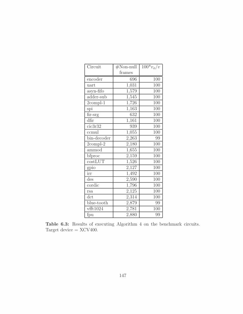
Circuit #Non-null 100*vφ/vframes
encoder 696 100uart 1,031 100asyn-fifo 1,579 100adder-sub 1,545 1002compl-1 1,726 100spi 1,163 100fir-srg 632 100dfir 1,161 100cic3r32 939 100ccmul 1,055 100bin-decoder 2,263 992compl-2 2,180 100ammod 1,655 100bfproc 2,159 100costLUT 1,526 100gpio 2,127 100irr 1,492 100des 2,590 100cordic 1,796 100rsa 2,125 100dct 2,314 100blue-tooth 2,879 99vfft1024 2,781 100fpu 2,880 99
Table 6.3: Results of executing Algorithm 4 on the benchmark circuits.Target device = XCV400.
147
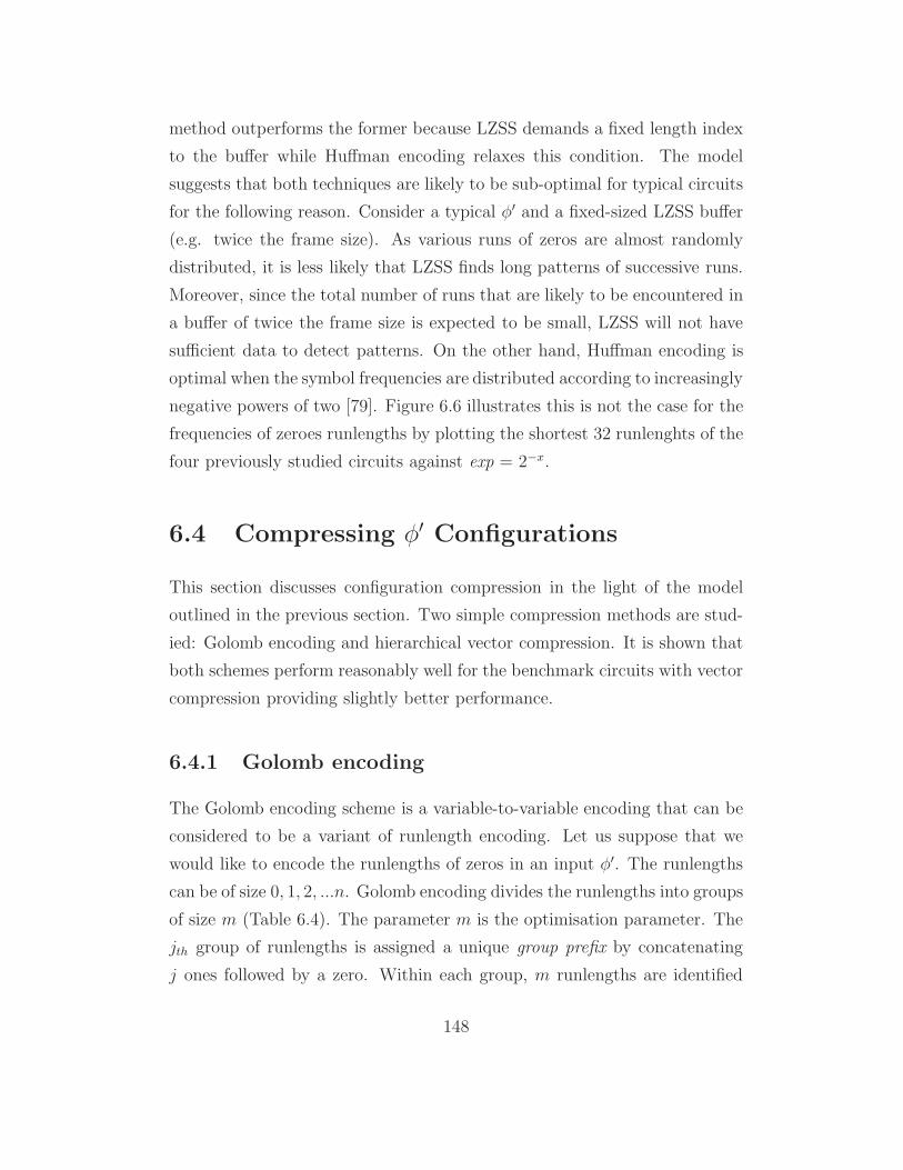
method outperforms the former because LZSS demands a fixed length index
to the buffer while Huffman encoding relaxes this condition. The model
suggests that both techniques are likely to be sub-optimal for typical circuits
for the following reason. Consider a typical φ′ and a fixed-sized LZSS buffer
(e.g. twice the frame size). As various runs of zeros are almost randomly
distributed, it is less likely that LZSS finds long patterns of successive runs.
Moreover, since the total number of runs that are likely to be encountered in
a buffer of twice the frame size is expected to be small, LZSS will not have
sufficient data to detect patterns. On the other hand, Huffman encoding is
optimal when the symbol frequencies are distributed according to increasingly
negative powers of two [79]. Figure 6.6 illustrates this is not the case for the
frequencies of zeroes runlengths by plotting the shortest 32 runlenghts of the
four previously studied circuits against exp = 2−x.
6.4 Compressing φ′ Configurations
This section discusses configuration compression in the light of the model
outlined in the previous section. Two simple compression methods are stud-
ied: Golomb encoding and hierarchical vector compression. It is shown that
both schemes perform reasonably well for the benchmark circuits with vector
compression providing slightly better performance.
6.4.1 Golomb encoding
The Golomb encoding scheme is a variable-to-variable encoding that can be
considered to be a variant of runlength encoding. Let us suppose that we
would like to encode the runlengths of zeros in an input φ′. The runlengths
can be of size 0, 1, 2, ...n. Golomb encoding divides the runlengths into groups
of size m (Table 6.4). The parameter m is the optimisation parameter. The
jth group of runlengths is assigned a unique group prefix by concatenating
j ones followed by a zero. Within each group, m runlengths are identified
148

0
0.05
0.1
0.15
0.2
0.25
0 5 10 15 20 25 30
Pro
babi
lity
of X
=i
Run size in bits (X=i)
"fpu_xcv400""exp"
(a) Circuit fpuxcv400
0
0.05
0.1
0.15
0.2
0.25
0.3
0 5 10 15 20 25 30P
roba
bilit
y of
X=
iRun size in bits (X=i)
"des_xcv400""exp"
(b) Circuit desxcv400
0
0.05
0.1
0.15
0.2
0.25
0 5 10 15 20 25 30
Pro
babi
lity
of X
=i
Run size in bits (X=i)
"bin_decod_xcv400""exp"
(c) Circuit bin-decodxcv400
0
0.05
0.1
0.15
0.2
0.25
0 10 20 30 40 50 60 70 80 90 100
Pro
babi
lity
of X
=i
Runsize in bits (X=i)
"exp""2compl-1_xcv400"
(d) Circuit 2compl-1xcv400
Figure 6.6: Comparing probability distribution of the shortes 32 runlengthsin four selected φ′ configurations with exp=2−x. Target device = XCV400.
149
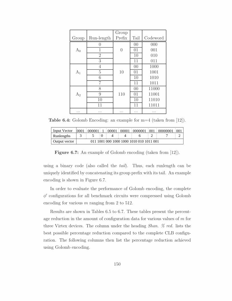
GroupGroup Run-length Prefix Tail Codeword
0 00 000A0 1 0 01 001
2 10 0103 11 0114 00 1000
A1 5 10 01 10016 10 10107 11 10118 00 11000
A2 9 110 01 1100110 10 1101011 11 11011
... ... ... ... ...
Table 6.4: Golomb Encoding: an example for m=4 (taken from [12]).
0001 00100000001001000000100001000001 1 00001Input VectorRunlengths
Output vector
272644053
011 1001 000 1000 1000 1010 010 1011 001
Figure 6.7: An example of Golomb encoding (taken from [12]).
using a binary code (also called the tail). Thus, each runlength can be
uniquely identified by concatenating its group prefix with its tail. An example
encoding is shown in Figure 6.7.
In order to evaluate the performance of Golomb encoding, the complete
φ′ configurations for all benchmark circuits were compressed using Golomb
encoding for various m ranging from 2 to 512.
Results are shown in Tables 6.5 to 6.7. These tables present the percent-
age reduction in the amount of configuration data for various values of m for
three Virtex devices. The column under the heading Shan. % red. lists the
best possible percentage reduction compared to the complete CLB configu-
ration. The following columns then list the percentage reduction achieved
using Golomb encoding.
150

Tables 6.5 to 6.7 demonstrate that Golomb encoding compresses the con-
figurations reasonably well. The φ′ configuration for the smallest circuit,
encoder on an XCV400, is compressed by 97.92% while the optimal com-
pression predicted by the entropic model is 99%. In general, the deviation
from the ideal increases with k. However, this increase is small compared to
the increase in k. For example, k increases from 4,394 to 155,387 which is al-
most a 36 fold increase. The difference between the ideal and real percentages
only increases from 1% to about 10% (for the case of the fpu circuit).
6.4.2 Hierarchical vector compression
This section discusses another technique for compressing sparse bit vectors.
This method is illustrated in Figure 6.8 (taken from [14]). Let us refer to
the uncompressed vector as Level-0 (l0) (in the example, |l0| = 27). This
vector can be compressed as follows. Partition the vector into equal sized
blocks each of size b0 bits. In the example, b0 has been taken to be three.
Next, drop the blocks that only contain zeros. However, this will not allow
us to reconstruct the original vector as we need to know where to insert the
zeros. Create a new vector (l1) whose length, |l1|, is equal to the number
of blocks at l0 (nine in this example). The leftmost bit of this new vector
corresponds to the leftmost block of the l0 vector, the second bit corresponds
to the second block and so on. A bit in the l1 vector is set if there is a set
bit in the corresponding block at l0. For example, the leftmost block in the
l0 vector has a set bit therefore the leftmost bit in the l1 vector is set.
The resulting l1 vector can now be compressed by applying the above
procedure recursively. In the example, it is assumed that the block size is
still the same, i.e. b1 = 3. The vector at l2 and the resulting compressed
vector are shown in Figure 6.8. This procedure can be repeated until a
reasonable compression is achieved. The number of levels lj and associated
block sizes, b0, b1..bj , are the optimisation parameters in this procedure.
The benchmark φ′ configurations for variously sized devices were exam-
151

101 110 101
Level−0
Level−1
Level−2
001 101 000 000 000 000 110 000 010
bits
001 101 110 010
000 101110
101
b
Figure 6.8: An example demonstrating the hierarchical vector compressionalgorithm. The uncompressed vector address is shown at Level-0. The re-sulting compressed vector is shown below the levels of compression (takenfrom [14]).
ined. The hierarchical vector compression was then applied to each φ′. The
lowest block size, b0, was varied from 2 to 128. Higher level block sizes were
set to be the same and between two and five levels of compression in total
were considered. The block size is therefore referred to as b in the following.
The best results were obtained for all circuits when three levels of com-
pression were used with b = 4 or b = 8. By three levels of compression it is
meant that the recursive compression procedure was stopped once the Level-
3 vector was produced. Tables 6.5 to 6.7 report the results for three Virtex
devices. It can be observed that vector compression performs within 5% of
the limit predicted by Shannon’s formula. It performs better than Golomb
encoding for small k but slightly worst for larger k. A second observation
is that its optimisation parameters, l and b, vary less as compared to the
optimisation parameter, m, of Golomb encoding.
6.5 ARCH-IV: Decompressing Configura-
tions in Hardware
The previous section showed that simple techniques such as Golomb encoding
and hierarchical vector compression perform reasonable compression when
152
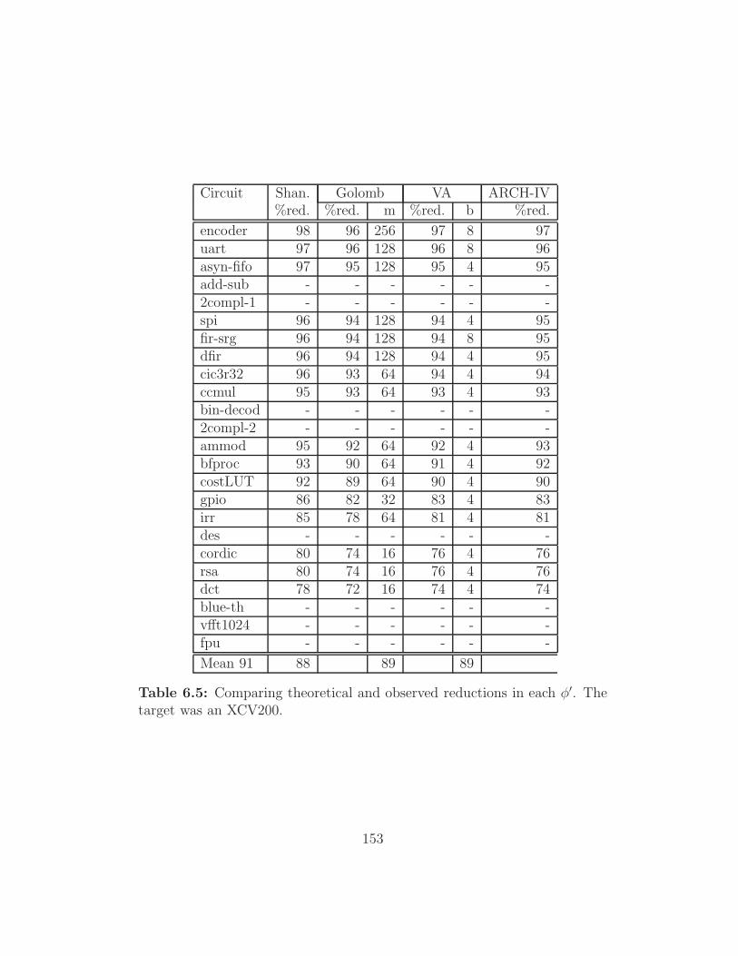
Circuit Shan. Golomb VA ARCH-IV%red. %red. m %red. b %red.
encoder 98 96 256 97 8 97uart 97 96 128 96 8 96asyn-fifo 97 95 128 95 4 95add-sub - - - - - -2compl-1 - - - - - -spi 96 94 128 94 4 95fir-srg 96 94 128 94 8 95dfir 96 94 128 94 4 95cic3r32 96 93 64 94 4 94ccmul 95 93 64 93 4 93bin-decod - - - - - -2compl-2 - - - - - -ammod 95 92 64 92 4 93bfproc 93 90 64 91 4 92costLUT 92 89 64 90 4 90gpio 86 82 32 83 4 83irr 85 78 64 81 4 81des - - - - - -cordic 80 74 16 76 4 76rsa 80 74 16 76 4 76dct 78 72 16 74 4 74blue-th - - - - - -vfft1024 - - - - - -fpu - - - - - -
Mean 91 88 89 89
Table 6.5: Comparing theoretical and observed reductions in each φ′. Thetarget was an XCV200.
153

Circuit Shan. Golomb VA ARCH-IV%red. %red. m %red. b %red.
encoder 99 98 256 98 8 97uart 99 98 256 98 8 97asyn-fifo 98 97 256 97 8 96add-sub 98 97 256 97 8 962compl-1 98 97 256 96 4 95spi 98 97 256 97 8 96fir-srg 98 96 256 97 8 96dfir 98 96 256 97 8 96cic3r32 98 96 128 97 8 96ccmul 98 96 128 96 8 95bin-decod 97 96 128 95 4 942compl-2 97 95 128 94 4 94ammod 97 95 128 95 8 95bfproc 97 94 128 94 4 94costLUT 96 94 128 94 4 93gpio 93 89 128 90 4 90irr 93 88 32 90 4 90des 89 85 32 86 4 86cordic 90 85 32 87 4 87rsa 89 84 32 86 4 86dct 89 84 32 86 4 86blue-tooth 78 73 16 74 4 74vfft1024 78 71 16 73 4 73fpu 69 63 16 62 4 62
Mean 93 91 91 90
Table 6.6: Comparing theoretical and observed reductions in each φ′. Thetarget was an XCV400.
154

Circuit Shan. Golomb VA ARCH-IV%red. %red. m %red. b %red.
encoder 99 99 512 99 8 99uart 99 99 512 99 8 99asyn-fifo 99 99 512 99 8 99add-sub 99 99 512 98 8 982compl-1 99 98 512 99 8 99spi 99 98 512 99 8 99fir-srg 99 98 512 99 8 99dfir 99 98 512 99 8 99cic3r32 99 98 512 99 8 99ccmul 99 98 512 98 8 98*bin-decod 99 98 512 97 8 97*2compl-2 99 98 256 97 8 97ammod 99 98 256 98 8 98bfproc 98 97 256 97 4 97costLUT 97 97 256 98 4 98gpio 97 95 256 95 4 95irr 97 95 128 96 8 96des 95 93 128 93 8 92cordic 96 92 64 94 8 94rsa 95 92 64 93 4 94dct 95 92 64 93 4 94blue-tooth 90 87 32 88 4 88vfft1024 91 85 32 88 4 88fpu 86 81 32 83 4 83
Mean 97 95 96 96
Table 6.7: Comparing theoretical and observed reductions in each φ′. Thetarget was an XCV1000.
155

compared with the fundamental entropy limit. For a set of benchmark cir-
cuits, it was found that both methods provide similar levels of performance.
Vector compression is preferred for hardware implementation because it is
simpler and provides slightly better performance.
This section presents ARCH-IV, which incorporates a hardware vector de-
compressor. The design of ARCH-IV is an enhancement of ARCH-II which
was discussed in Chapter 5. ARCH-IV is designed with b = 4 and a con-
figuration port width of 4-bits. It is assumed that vector compression is
performed to the height of three levels.
6.5.1 Design challenges
This section discusses various challenges associated with the decompressor
design. In order to motivate the discussion, please consider Figure 6.9 which
illustrates a general model of a memory. Data is written into the memory
via a port while an internal controller generates the necessary signals for the
network and for the array in order to perform a read or a write operation.
The required on-chip decompressor not only needs to interface with the
memory controller but also with the data distribution network. With the
designs of Chapter 5 in mind, the first design requirement is that the decom-
pressor should decompress at the same rate as data is input to the device
thereby translating the compression gain into a reduction in reconfiguration
time. This constraint demands a higher bandwidth from the on-chip data
distribution network. In other words, the network should allow the distribu-
tion of uncompressed data from the decompressor to the memory array at
the same rate at which data is being uncompressed.
On the flip side of the coin, reconfiguration time should decrease as the
port size is increased. This requirement means that the decompressor should
scale with an increase in the port size and should still be able to match the
externally available bandwidth with the internal bandwidth. The problem is
complicated by the fact that different circuit configurations are compressed
156

Port Port
MemoryCell Array
Cell ArrayMemory
Decompressor
Controller
Network
Network
Controller
Figure 6.9: The environment of the required decompressor.
to different degrees and therefore one cannot simply fix the ratio between the
internal and external bandwidths.
Lastly, the configuration memory of an FPGA shares VLSI resources with
the computational plane (CLBs, switches and the user IO pins) and therefore
must not demand significant additional chip area.
6.5.2 Solution strategy
In order to simplify the design of the decompressor, the design of the internal
network is fixed. It is assumed that the memory array is implemented using
SRAM cells and sufficient on-chip bandwidth exists for the decompressor to
write one frame of data to the destination register within a single cycle. Vir-
tex provides such a mechanism. A two-dimensional mesh of control and data
wires is needed to fulfil this requirement. This network model is already well
established in the memory design arena. No doubt more elaborate network
models can be conceived. Modern chips contain several metal layers and thus
a tree-like network that mirrors the hierarchical compression scheme can be
designed. However, such designs are likely to demand significant additional
area and would thus be less attractive for designers of future FPGAs.
157

As stated above, it is assumed that an SRAM-style internal interconnect is
available whereby the required decompressor can access at most one frame at
a time. The decompressor therefore can perform decompression on a frame-
by-frame basis. The input data is also compressed on a frame-by-frame basis
using the hierarchical compression method. Later it is shown that frame-
by-frame compression yields results similar to those for device-level vector
compression.
Please note that the block size that is used in the vector compression
is not considered to be an indepedant variable in the decompressor design.
This is because it was previously shown that a fixed block size of b = 4
is sufficiently good for all circuits on Virtex devices and b = 8 is the next
best choice. The same is true for the number of compression levels used,
which is fixed at three. These results will be confirmed again for frame-level
compression. With these decisions, the main concern is the scalability of the
decompressor with increasing device size and with increasing configuration
port width.
6.5.3 Memory design
ARCH-II is enhanced to incorporate a vector decompressor resulting in
ARCH-IV. The new memory internally generates null frames in the same
manner as ARCH-II while the input φ′ configuration is being decompressed.
The generated null frames are then modified based on the uncompressed φ′
data before writing to the target frame registers.
In ARCH-IV, the vector decompressor receives φ′ vectors (Figure 6.10)
and outputs uncompressed data into the mask register. The size of the null
frame register is set to f bits. Once the mask register is full, i.e. it contains
a complete frame of φ′, the contents of the null frame are written into the
intermediate register based on the contents of the mask register. A bit in
the null frame register is written to the intermediate register as is if the
corresponding bit in the null frame is cleared, otherwise it is complemented.
158

The memory operates in a pipelined fashion. As decompressing a frame
can take several cycles, the null frame generator is used in the background
to generate null frames for the null blocks. The null blocks address is stored
in the NBA register. When a φ′ vector for a frame is ready, the null frame
generator is switched to generate a null frame for the user block address
(UBA register) instead of the null block address. The required user frame
is then written to the intermediate register as explained above. The process
iterates until all user frames have been loaded. When there are many more
null than user frames to be written, configuration may need to continue
after decompression has finished to complete circuit loading. The worst case
scenario is that only 1 bit per user frame needs to be loaded. For an XCV400,
such a frame can be decompressed in 7 cycles, thus if such a pathological
configuration has more than 7 times as many null frames it will need to wait
after loading is completed before the device is available for use. Typical
configurations need many more cycles on average to load user frame data,
and therefore provide ample time for all null frames to be loaded in the
background. As an example, consider the circuit encoder on an XCV400.
The total amount of VA data for this circuit is only 2% of the complete
XCV400 bitstream size. This amounts to around 5,760 bytes which is almost
double the total number of frames in the device (2,880).
6.5.4 Decompressor design
The configuration port size in the new memory is set to 4 bits so that it
matches the block size. As three levels of compression are used, four bits of
the Level-3 vector span 256 bits at Level-0. The decompressor therefore op-
erates in units of 256 bits (Figure 6.11). These units are sequentially selected
using a control shift register which is initialised by asserting the topmost bit.
The Vector Address (VA) decoding system performs decompression of the
input φ′ vector and outputs 64 bits of the Level-0 vector at a time. This 64-
bit word is temporarily stored in the vector-address-decoder register (VAD
159

4
Inte
rmed
iate
Reg
iste
r
Nul
l Fra
me
Reg
iste
r
Mas
k R
egis
ter
Null FrameGenerator
Decompressor
Memory Array
RegisterNBA
Register
Address Decoder
Configuration State Machine
From Interface Circuit
Data
Legend
Signal
Configuration
UBA
16
54
Control
f
64
Figure 6.10: The proposed memory architecture.
register). At the same time, the VA decoding system outputs a 4-bit control
word in the data-forwarding control (DFC) register. This 4-bit word selects
one of the four 64-bit registers currently selected by the control shift-register.
The decompressor reads in a φ′ and sequentially updates the entire mask reg-
ister 64-bits at a time. Once 256-bits of a unit are updated, the control shift
register is signalled and the next unit is selected. The cycle repeats until all
units in a frame are updated. Note that there can be a final partial block
in the mask register because Virtex frames are not always a multiple of 256
(e.g. XCV400 has an 800-bit frame).
The architecture of the VA decoding system is shown in Figure 6.12. The
VAD register is a 4×16 register controlled by a 16-bit word which selects one
of the 4-bit registers at a time. A hierarchical vector is decoded by traversing
the various compressed levels in parallel. The Level-i vector is latched into
the V ADi register one 4-bit compressed VA word at a time. Each register
produces a sequence of 4-bit output vectors that respectively indicate which
bits in the VA word, from most to least significant, are set. In turn, the
160

VAD Register
64
64
64
64
DFC Register
8f%64
64
64
64
Con
trol
Shi
ft R
egis
ter
DF
Reg
iste
r
VA Decoding System
Configuration State Machine
Figure 6.11: A high-level view of the decompressor.
V AD1 output vectors indicate which 4-bit block of the VAD Register the
next 4 bits from the interface circuit (corresponding to l0) are written to.
V AD2 output vectors control which block of 16 bits the V AD1 vectors refer
to, and the V AD3 vectors determine which 64-bit block of the mask register
the VAD Register contents are written to. The internal details of a VAD can
be found Section 5.3.2.
6.5.5 Design analysis
As discussed in the previous section, the approach followed in the ARCH-IV
design is to perform decompression on a frame-by-frame basis. This method
is likely to increase the size of the compressed bitstream as the frame sizes
cannot always be an integral multiple of bj+1. Due to this factor, additional
161
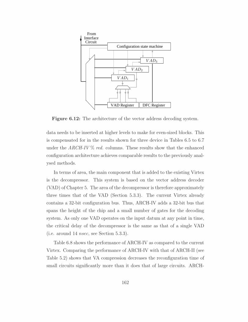
CircuitInterface
From
VAD Register DFC Register
Configuration state machine
V AD3
V AD2
V AD1
Figure 6.12: The architecture of the vector address decoding system.
data needs to be inserted at higher levels to make for even-sized blocks. This
is compensated for in the results shown for three device in Tables 6.5 to 6.7
under the ARCH-IV % red. columns. These results show that the enhanced
configuration architecture achieves comparable results to the previously anal-
ysed methods.
In terms of area, the main component that is added to the existing Virtex
is the decompressor. This system is based on the vector address decoder
(VAD) of Chapter 5. The area of the decompressor is therefore approximately
three times that of the VAD (Section 5.3.3). The current Virtex already
contains a 32-bit configuration bus. Thus, ARCH-IV adds a 32-bit bus that
spans the height of the chip and a small number of gates for the decoding
system. As only one VAD operates on the input datum at any point in time,
the critical delay of the decompressor is the same as that of a single VAD
(i.e. around 14 nsec, see Section 5.3.3).
Table 6.8 shows the performance of ARCH-IV as compared to the current
Virtex. Comparing the performance of ARCH-IV with that of ARCH-II (see
Table 5.2) shows that VA compression decreases the reconfiguration time of
small circuits significantly more than it does that of large circuits. ARCH-
162

IV offers an additional benefit of eliminating the mask control circuitry from
ARCH-II.
ARCH-IV assumes a 4-bit configuration port. This system can be readily
scaled to wider port sizes. Assume that the port size is increased from 4 to 4p
where p is a strictly positive integer. The system is scaled by implementing
p decompressors each with its own mask register. Each p is assigned a 4-bit
portion of the port and operates independently of the other decompressors.
The p decompressors share a single 64-bit bus to reach their assigned mask
register, When a particular decompressor is ready to write its 64-bit word
to its mask register, it asserts a bus request signal. As several decompressors
can assert this signal simultaneously, a priority decoder is used to resolve bus
conflicts. The decompressors that are waiting to access the bus are stalled
and the user needs to insert dummy data to the bitstream to account for
this.
As the port size is increased from 4-bits to 4p bits, reconfiguration time
ideally decreases by a factor of p. However, the proposed architecture is
likely to pose some additional overhead due to port stalling. The operation
of ARCH-IV was simulated for various values of p. The simulation method is
similar to that is presented in Appendix C. The number of cycles needed to
configure each benchmark circuit on an XCV400 was determined. For each
circuit, a reduction factor was computed by dividing the number of cycles at
the port size under consideration by the number of cycles needed in the base
case which was taken to be p = 1. Figure 6.13 shows the mean reduction
factors over all circuits for various values of p.
Table 6.9 compares the overall performance of ARCH-III and ARCH-IV.
The first column lists the port size in bits. The second and third columns list
the mean reconfiguration time on ARCH-III and ARCH-IV respectively when
compared to Virtex. This figure is calculated from the last rows of Tables
5.2 and 6.8. The rows of Table 6.9 are calculated from the data plotted in
Figures 5.15 and 6.13. For example, when p = 2, ARCH-III and ARCH-
IV reduce reconfiguration time by a factor of 0.51 and 0.57 respectively.
163

Circuit % ReductionXCV200 XCV400 XCV1000
encoder 90 92 94uart 91 95 97asyn-fifo 92 95 98add-sub - 95 952compl-1 - 94 98spi 89 93 97fir-srg 82 90 97dfir 89 94 97cic3r32 89 92 94ccmul 87 89 92bin-decod - 94 962compl-2 - 92 95ammod 86 91 96bfproc 84 92 96costLUT 83 90 91gpio 81 87 92irr 77 83 90des - 84 93cordic 75 79 89rsa 73 81 86dct 72 83 83blue-th - 74 87vfft1024 - 72 82fpu - 62 79
Mean 98 87 92
Table 6.8: Percentage reduction in reconfiguration time of ARCH-IV com-pared to current Virtex.
164

0
0.1
0.2
0.3
0.4
0.5
0.6
0.7
0.8
0.9
1
2 4 6 8 10 12 14 16
Mea
n re
duct
ion
fact
or
Port size p (bytes)
"Ideal""ARCH-IV"
Figure 6.13: The overhead of ARCH-IV for large sized ports.
Thus, the mean reconfiguration time of these devices at a port size of 16 bits
is calculated to be 19% and 3% of Virtex reconfiguration time. Table 6.9
suggests that, assuming typical circuits, reconfiguration time of ARCH-IV is
almost negligible compared to Virtex even at medium sized ports.
While ARCH-IV can be scaled well for practical port sizes, it can be
further enhanced. One method to reduce the contention over the DF bus
is to pipeline the operation of forwarding the frames to the memory array.
Figure 6.14 shows an enhanced ARCH-IV, which splits the memory array into
two halves, labelled top and bottom. The intermediate register is also split
into two halves. The idea is when the top half of a frame is updated in the
top half of the DF register of a decompressor, it is immediately scheduled for
a transfer to the top half of the intermediate register while the decompressor
operates on the bottom half of the frame. If a circuit spans both top and
bottom of the device then some of the delay that arises due to contention
over the DF-Bus in ARCH-IV can be hidden.
165

Port size %Reconfiguration Time(bits) of Virtex
ARCH-III ARCH-IV
8 38 516 19 332 11 264 6 2
128 4 2
Table 6.9: Percentage reduction in mean reconfiguration time for the bench-mark set of ARCH-IV compared to current Virtex.
Additional hardware is necessary to control the scheduling of the two
memory planes. Firstly, we need another decoder to select one of the two
halves for a write operation. Secondly, the DF-Bus arbiter has to be shared
between the two halves. We do not need to replicate the DF-Bus arbiter as
only one of the halves can be written to in any one cycle, therefore needing
only one arbiter that can be shared among the two halves of each decom-
pressor.
It is envisaged that the above method of pipelining ARCH-IV applies to
devices such as Virtex-4 [124]. These FPGAs have a fixed-sized frame and
appear to have several memory pages that span the entire width of the device
(similar to the arrangement shown in Figure 6.14).
6.6 Conclusions
This chapter has three main contributions.
• It has developed the idea of entropy of reconfiguration an objective
measure of configuration compression quality. The entropy of reconfig-
uration for a set of benchmark circuits was measured and shown to be
almost constant indepedant of the circuit and device sizes.
• It has shown that simple off-the-shelf techniques such as Golomb en-
166

Address Decoder
Memory ArrayBottom
Memory ArrayTop
Inte
rmed
iate
Reg
iste
rT
opIn
term
edia
te R
egis
ter
Bot
tom
From
Dec
ompr
esso
rs
Configuration State Machine
Figure 6.14: Pipelining the operation of loading the frames.
coding and hierarchical vector compression perform reasonable com-
pression of the configurations under test.
• It has presented new scalable configuration architectures that incor-
porate a configuration decompressor system inside the FPGA. These
systems have shown to translate the reduction in configuration data,
made possible by compression, into a proportionate reduction in recon-
figuration time.
167

The above analysis, however, ignores the power dissipation which in-
creases by at least the same proportion by which reconfiguration time is de-
creased. The power increases because of the increased rate at which switches
are flipped inside the memory in order to store configuration frames. ARCH-
IV can easily be further enhanced to allow the user to vary the configuration
port size during reconfiguration. Thus, depending on the applications, re-
configuration speed can be traded off against reconfiguration power.
The analysis of this thesis suggests that if the null configuration of a device
entirely consists of zeroes then there are only a small number of bits that need
to be flipped in the memory during reconfiguration. This fact can possibly
be used to design a memory that is power efficient during reconfiguration.
Such a memory will only switch on those rows of the SRAM cells where there
is a set bit to be written as opposed to ARCH-IV where all rows of the device
are simultaneously switched on for a write operation.
168

Chapter 7
Configuration Encoding for
Generic Island-Style FPGAs
7.1 Introduction
The thrust of this thesis is to reduce reconfiguration time of an FPGA at
its configuration data level. In particular, the aim is to reduce the amount
of configuration data that needs to be loaded onto the device in order to
configure a given circuit. So far, the thesis has examined various methods to
reduce the amount of configuration data corresponding to typical circuits on
Virtex FPGAs [123]. This chapter examines the application of these methods
to a wider class of island-style FPGAs.
The previous chapters have presented several characteristics of typical
Virtex configurations which were formalised into an entropic model of config-
uration data in Chapter 6 (see Figure 7.1). The model views Virtex configu-
rations as mainly consisting of null data with a small amount of non-null data
randomly distributed over the area spanned by the input circuit. The benefit
of this model is that it predicts the size of the compressed bitstream that an
optimal runlength compression method outputs and therefore allows us to
compare the performance of various proposed compression techniques. Sev-
169

Efficient Compression/
DecompressionTechniques
Results
Configuration Model of
Data
Prediction
Configuration Data
Figure 7.1: The approach followed in this thesis.
eral empirical tests have shown that the assumptions underlying the model
are valid and that its predictions are accurate for practical purposes. The
previous chapters also showed that existing compression methods, such as
vector compression, offer reasonable performance in practice.
Virtex devices are general purpose FPGAs and it can be claimed that the
results obtained on these devices have a certain degree of generality. Never-
theless, it is instructive to examine how well the methods of previous chapters
stand the empirical tests on non-Virtex FPGAs. This chapter tests the ap-
plication of the previously described configuration model for a wider class of
FPGAs. It is shown that the model reasonably predicts the bounds on com-
pression for a set of benchmark circuits on hypothetical FPGA architectures.
Therefore, this chapter examines the performance of vector compression and
Golomb encoding for a set of benchmark circuits on the assumed FPGAs and
shows that vector compression remains a practical and efficient compression
method. Section 7.2 outlines the testing method and also serves as a guide
to the rest of the chapter.
7.2 Experimental Method
The goals of these experiments are to show that:
170

• The characteristics of Virtex configurations remain true for various
other island-style FPGAs. In particular:
– The configurations are sparse, i.e. k << n.
– The distribution of various runlengths in each configuration fol-
lows an exponential curve.
– The runlengths are randomly distributed.
• Vector addressing performs well as compared to the fundamental com-
pression limit.
The approach followed is to consider a range of hypothetical architectures
that are representative of real FPGAs and a set of benchmark circuits that
have been extensively used by others to study these architectures. Each
circuit was mapped onto the chosen architectures and configuration data for
these devices was generated. These configurations were then fed into various
programs that were previously used to analyse Virtex configurations.
A simulation environment was set up to experiment with hypothetical
FPGA architectures. The goal of the simulation environment was to generate
the final bitstream, that when loaded onto the hypothetical device, configures
the circuit. This environment was the core of the experimental method and
is therefore discussed in detail in subsequent sections. Here, an overview is
provided.
Figure 7.2 illustrates the experimental setup. TVPack and VPR are open
source CAD tools that are used for the research of FPGA architectures, CAD
algorithms and designflows [4, 119]. These tools accept a high-level descrip-
tion of an FPGA architecture and a BLIF netlist of a circuit. The tools
automatically map the input circuit onto the specified architecture and out-
put details of the final mapping. The tools also output some of the imple-
mentation details of the FPGA such as the total amount of area needed to
implement the device using specified VLSI parameters. Section 7.3 provides
a brief description of these tools while details can be found in [119].
171

VPRConfigGen
TVPack/VPR
DescriptionCircuit
Bit File
Analysis Tools
Detailed Descriptionof Architecture
High−levelDescription of
Architecture
ConfigurationModel of
Memory
Description of Placedand Routed Circuit
Figure 7.2: The experimental setup.
A set of programs, collectively referred to as VPRConfigGen, was devel-
oped in order to generate the final configuration data. Input to VPRCon-
figGen is the low-level description of the mapped circuit, the high-level de-
scription of the circuit and implementation details of the specified FPGA
architecture. The output is configuration data for the specified architecture
in various formats. Section 7.4 describes the operation of these programs in
more detail.
TVPack/VPR and VPRConfigGen together provide an environment in
which one can specify an FPGA architecture at a high-level and can produce
configuration data for a given circuit targeted to the specified architecture.
With this experimental setup, the next step is to select candidate architec-
tures and a set of benchmark circuits. Since both architecture and circuit
spaces are large, it is difficult to examine all possibilities. An additional
problem is that placement and routing algorithms consume considerable pro-
cessing time. Therefore, only a small number of circuits can be examined on
a small number of architectures in a reasonable amount of time. For this
172

research, the 20 largest circuits in the MCNC suite [100] were chosen as
suitable benchmark (also known as Toronto 20). These circuits are chosen
because they are large in size and are available in a format understood by
the TVPack/VPR tools.
The approach taken to narrow down the architecture space is illustrated in
Figure 7.3, which maps architecture points onto a two dimensional space. An
architecture point contains devices that have the same structure but different
levels of resources. In the space depicted in Figure 7.3, each point represents
devices of the same architecture but different sizes. A horizontal line in the
space is referred to as an ARCHRouting subspace. Architecture points that lie
on these line have the same logic architecture but they differ in their routing
architecture. Similarly, vertical lines are referred to as ARCHLogic subspaces.
Virtex and Virtex-II lie in the same ARCHRouting subspace. It appears that
the logic architecture of Virtex-4 devices is similar to that of Virtex-II devices.
However, little details could be found on the routing architecture of Virtex-
4. Virtex-II and Virtex-4 therefore lie on the same ARCHLogic subspace but
they might lie on different ARCHRouting subspaces.
The approach followed in this chapter is to first examine an architecture,
ARCHx, that closely resembles Virtex. A set of benchmark circuits are
mapped onto ARCHx using the simulation environment discussed above.
The resulting configuration data is subjected to the analysis reported in
the previous chapters. The aim of this experiment is to show that a small
deviation in Virtex architecture does not result in any significant changes in
the results. More precisely, the experiments with ARCHx aim to show:
• The amount of non-null data is small compared to the size of the com-
plete configuration bitstream.
• The model of configuration data that was derived in Chapter 6 is a
reasonable approximation and one can therefore gauge the size of the
smallest possible configuration for a given mapped circuit.
173

Rou
ting
plan
e
Complex
Logic planeSimple Complex
Virtex−IV?Virtex−II
Simple
Virtex
ARCHLogic subspaces
ARCHRouting subspaces
ARCHCLB subspace
ARCHsegment subspace
ARCHx
Figure 7.3: FPGA architecture space.
• Vector compression and Golomb encoding provide reasonable compres-
sion compared to the maximum possible compression.
Sections 7.5 and 7.6 describe the above experiments and show that the
above statements hold for typical ARCHx configurations.
The next step was to examine a wider architecture space. Traversing the
entire, or even a moderately large part of, the entire architecture space is
too difficult in practice. This chapter examines two sub-spaces, ARCHCLB
and ARCHsegment, that lie orthogonal to each other. Devices in ARCHCLB
differ from each other in terms of the CLB size while devices in ARCHsegment
differ from each other in terms of the distribution of various wire segment
lengths. Section 7.7 examines the impact of changing the number of look-up-
tables in a CLB on the overall reconfiguration time of the circuit. A range
of device architectures is examined. For the benchmark circuits it is shown
that, in general, a medium-sized CLB offers a reasonable compromise between
reconfiguration time, FPGA area and circuit frequency. Section 7.8 extends
this analysis to include the channel routing architecture of the FPGA. It
174

shows that for the circuits under test, the channel routing architecture of the
target device has lesser impact on the overall reconfiguration time. It should
be pointed out that the term routing architecture generally includes the CLB
connection blocks as well. In the light of these results, Section 7.9 discusses
configuration architectures for a generic island-style FPGA.
7.3 TVPack and VPR Tools
TVPack and VPR are open source CAD tools that have been extensively
used in research on FPGA architectures. The overall flow employed by this
design suite is shown in Figure 7.4. An input circuit is first synthesised using
logic optimisation tools such as SIS [82]. The resulting netlist is technology
mapped using FlowMap [18] which outputs a .blif file [105]. The .blif file is
fed into TVPack, which clusters the logic gates in the input netlist into the
target logic elements. The output of TVPack is a technology-mapped netlist
in .net format.
The input to VPR is a description of an island-style (or mesh-like) FPGA
architecture and a technology-mapped netlist in .net format. It maps the
input circuit onto the target device and outputs a placed and routed circuit.
The user specifies the target device in a .arch file. This file contains values
of various device parameters. These device parameters are explained with
reference to Figure 7.6. An FPGA is taken to be an array of CLBs, or logic
clusters, surrounded by a routing network. The building block of a CLB is
called a basic logic element (BLE). A BLE consists of an l input LUT, and
an optional Flip-Flop (FF) as shown in Figure 7.5. The number of BLEs
per CLB is specified by a parameter m. The total number of inputs, I, to
each CLB is therefore l ×m and the number of outputs, O, is m. We ignore
the clock and reset inputs for simplicity. Within a CLB, each input of each
BLE can connect to any of the I inputs and to any of the O outputs. These
connections can be made using multiplexors that are referred to as imuxs.
175
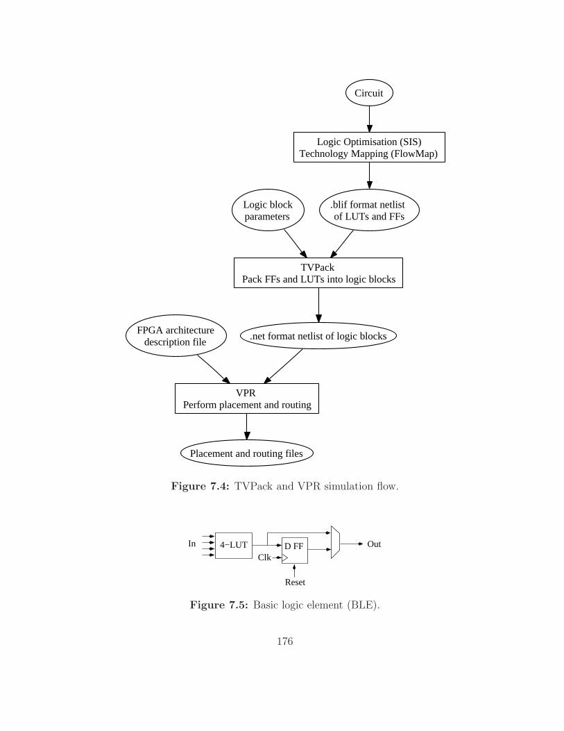
Logic Optimisation (SIS)Technology Mapping (FlowMap)
.blif format netlist of LUTs and FFs
TVPack Pack FFs and LUTs into logic blocks
.net format netlist of logic blocks
VPR Perform placement and routing
Placement and routing files
Logic blockparameters
FPGA architecturedescription file
Circuit
Figure 7.4: TVPack and VPR simulation flow.
D FF4−LUTClk
In Out
Reset
Figure 7.5: Basic logic element (BLE).
176

The routing architecture consists of switch blocks and connection blocks.
Switch blocks can be programmed by the user to connect together wires in
the channels. VPR supports various types of switches such as disjoint, Wilton
and universal switches. A detailed description of these switch types can be
found in [51]. The present work focuses on the disjoint switch. This switch is
characterised by the number of tracks in a channel, W . Even though W can
vary from one channel to another, we assume that all channels are uniform.
Given this assumption, there are W programmable interconnect points per
switch block.
The user can construct a hierarchical interconnect by varying the length
of various wires in each channel. The length of a wire is specified by the
number of CLBs it spans. Figure 7.7 shows an example of a hierarchical
architecture. The proportion of different length wires in the channels is an
architectural parameter that can be specified for VPR. It should be noted
that wires of length greater than 1 have different starting positions in different
horizontal and vertical channels. VPR performs this staggering to produce
valid architectures and to improve routability.
Input and output connection blocks, in Figure 7.6, connect a CLB to its
neighbouring switches. An input connection block is implemented as a set
of multiplexors that connect a track in the neighbouring routing channel to
a CLB input pin. The internal population of an input connection block is
specified by the parameter Fcinput. This fraction specifies the proportion of
the wires that can be connected to the CLB inputs. For example, Fcinput =
0.5 means that a CLB can take its input from only half of the available wires
in the neighbouring channel. The output connection blocks are specified
by the parameter Fcoutput which has a similar meaning. Output connection
blocks are slightly different from the input connection blocks in the sense
that a CLB output can drive multiple wires. The internal switches of an
output connection block are therefore implemented as pass transistors. The
parameters sb and cb refer to the switch and connection block population
respectively. These fractions determine the percentage of the tracks that are
177

Routing Channel
Out
put C
onne
ctio
n B
lock
Inpu
t Con
nect
ion
Blo
ck
BLE 0
0
Switch Switch
CLB
(W )
(l, m)
BLE m − 1
l-1
(Fc i
npu
t)
(Fc o
utp
ut)
I inputs O outputs(m)(l × m)
Figure 7.6: FPGA architecture definition.
CLB CLB CLB CLB CLB CLB CLB
WLength 1 wires
Long lineLength 2 wires
Length 1 wires
Routing Channel
Figure 7.7: Hierarchical routing in an FPGA. Connections between thetracks and the CLBs are not shown.
178

Parameter Description Typicalvalue
l Number of inputs per LUT 4-6m Number of LUTs per CLB 4-8W Number of tracks per channel Circuit size dependantFcinput Input connection block population 0.5-1.0Fcoutput Output connection block population 0.5-1.0sb Switch block population 1.0cb Connection block population 1.0Switch type Routing switch type Disjoint, Wilton,
UniversalSegements lengths The length of the routing wires 1,4, chip-length
Table 7.1: Various parameters of VPack/VPR and their typical values.
connected by the respective blocks.
Table 7.1 provides a list of the above parameters and their typical values.
VPR tools take many more parameters but they are less relevant to the sub-
sequent discussion. Unless otherwise stated, these parameters are assumed
to take their default values which are listed in [119].
7.4 VPRConfigGen Tools
A set of Java programs, VPRConfigGen, was developed to generate configu-
ration data from the files output by the TVPack/VPR tools. The procedure
employed by VPRConfigGen is described below in detail.
7.4.1 CLB configuration
CLB configuration consists of LUT contents, imux settings, clock and reset
signals. The last two are ignored in this analysis. VPR does not keep a
track of the LUT contents during its operation. This is because it is a
place and route tool and this information is not important for its operation.
Nevertheless, the input .blif file contains a description of the logic gates that
are to be mapped onto the device. The input .blif file is parsed by converting
179
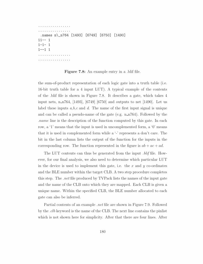
................
................
.names n\_n764 [1493] [6749] [6750] [1490]
11-- 1
1-1- 1
1--1 1
................
................
Figure 7.8: An example entry in a .blif file.
the sum-of-product representation of each logic gate into a truth table (i.e.
16-bit truth table for a 4 input LUT). A typical example of the contents
of the .blif file is shown in Figure 7.8. It describes a gate, which takes 4
input nets, n n764, [1493], [6749] [6750] and outputs to net [1490]. Let us
label these inputs a,b,c and d. The name of the first input signal is unique
and can be called a pseudo-name of the gate (e.g. n n764). Followed by the
.name line is the description of the function computed by this gate. In each
row, a ‘1’ means that the input is used in uncomplemented form, a ‘0’ means
that it is used in complemented form while a ‘-’ represents a don’t care. The
bit in the last column lists the output of the function for the inputs in the
corresponding row. The function represented in the figure is ab + ac + ad.
The LUT contents can thus be generated from the input .blif file. How-
ever, for our final analysis, we also need to determine which particular LUT
in the device is used to implement this gate, i.e. the x and y co-ordinates
and the BLE number within the target CLB. A two step procedure completes
this step. The .net file produced by TVPack lists the names of the input gate
and the name of the CLB onto which they are mapped. Each CLB is given a
unique name. Within the specified CLB, the BLE number allocated to each
gate can also be inferred.
Partial contents of an example .net file are shown in Figure 7.9. Followed
by the .clb keyword is the name of the CLB. The next line contains the pinlist
which is not shown here for simplicity. After that there are four lines. After
180

................
................
.clb [846]
pinlist: ...............
subblock: [n\_n764] .......
subblock: [1354] .......
subblock: [1833] .......
subblock: [6495] .......
................
................
Figure 7.9: An example entry in a .net file.
the key word subblock :, there is a list of input/output nets. The pseudo-
name appears as the first signal and can be matched with its entry in the
.blif file. The order in which gates appear in a .clb statement is taken to
be their subblock number. VPRConfigGen maintains an internal list of the
block number that has been assigned to each gate within a CLB. The actual
(x, y) co-ordinates of each CLB are determined from the .place file output
by VPR. A .place file simply lists the names of all CLBs and their x and y
co-ordinates.
The .net file produced by TVPack is also used to generate the imux
configuration. In an architecture with 4 BLEs/CLB, there will be 16 inputs
and 4 outputs. There will be 16 imuxes corresponding to the LUT inputs.
Each imux will be a 20:1 device needing 5 bits for its configuration.
7.4.2 Switch configuration
The procedure to generate routing configuration operates on the .route file
which is output by VPR. An example of a .route file is shown in Figure 7.10.
Switch configuration is generated every time a net passes from a track in one
channel to another track in a different channel. It should be noted that a net
cannot change track numbers if the switch type used is subset. It is assumed
that each programmable interconnect point (PIP) in the subset switch is
181
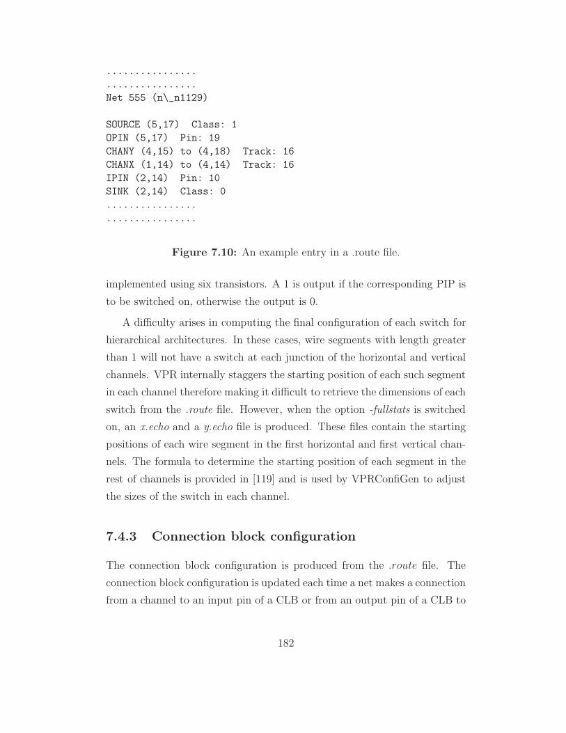
................
................
Net 555 (n\_n1129)
SOURCE (5,17) Class: 1
OPIN (5,17) Pin: 19
CHANY (4,15) to (4,18) Track: 16
CHANX (1,14) to (4,14) Track: 16
IPIN (2,14) Pin: 10
SINK (2,14) Class: 0
................
................
Figure 7.10: An example entry in a .route file.
implemented using six transistors. A 1 is output if the corresponding PIP is
to be switched on, otherwise the output is 0.
A difficulty arises in computing the final configuration of each switch for
hierarchical architectures. In these cases, wire segments with length greater
than 1 will not have a switch at each junction of the horizontal and vertical
channels. VPR internally staggers the starting position of each such segment
in each channel therefore making it difficult to retrieve the dimensions of each
switch from the .route file. However, when the option -fullstats is switched
on, an x.echo and a y.echo file is produced. These files contain the starting
positions of each wire segment in the first horizontal and first vertical chan-
nels. The formula to determine the starting position of each segment in the
rest of channels is provided in [119] and is used by VPRConfiGen to adjust
the sizes of the switch in each channel.
7.4.3 Connection block configuration
The connection block configuration is produced from the .route file. The
connection block configuration is updated each time a net makes a connection
from a channel to an input pin of a CLB or from an output pin of a CLB to
182

a channel. The size of the connection block is determined from the number
of tracks in each channel and the number of inputs and outputs per CLB.
7.4.4 Configuration formats
The final configuration bitstream is output to three different files. The
pseudo-code for this last step is shown in Figures 5 to 7. These bitfiles are
then analysed with various programs as discussed in the following sections.
The first format is output by first visiting each CLB in the array and
outputting its configuration. Then, each connection block is visited and
its configuration output. Lastly, each switch configuration is output. The
traversal is in the row major order. The second format visits the location
(x, y) and outputs CLB, connection block and switch block configuration
in the same order. The third format outputs the configuration at location
(x, y) by following the flow of signals from a routing channel to a CLB output,
i.e. input connection block, imux, CLB, output connection block and switch
block.
7.5 Measuring Entropy of Reconfiguration
The set of 20 MCNC benchmark circuits was considered. An experimental
architecture, ARCHx, was defined for the TVPack/VPR CAD tools. The
parameters of this design are listed in Table 7.2. The 20 circuits were mapped
onto ARCHx and configuration data in three different formats was generated.
Table 3 lists the circuits and their important parameters. The first column
lists the circuit name. The second lists the total number of BLEs used to
map the circuit. The next column lists the total number of CLBs needed.
The third column list the total number of nets in the circuit. These figures
are reported by TVPack. The next two columns list the number of CLB rows
and columns needed to route the circuit on ARCHx. The column under the
heading Clb cfg lists the total amount of CLB configuration data needed for
183
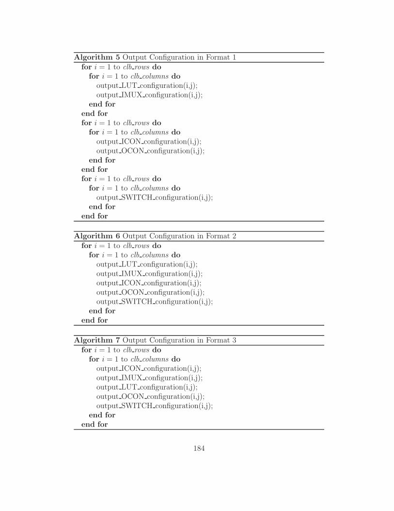
Algorithm 5 Output Configuration in Format 1
for i = 1 to clb rows dofor i = 1 to clb columns do
output LUT configuration(i,j);output IMUX configuration(i,j);
end forend forfor i = 1 to clb rows do
for i = 1 to clb columns dooutput ICON configuration(i,j);output OCON configuration(i,j);
end forend forfor i = 1 to clb rows do
for i = 1 to clb columns dooutput SWITCH configuration(i,j);
end forend for
Algorithm 6 Output Configuration in Format 2
for i = 1 to clb rows dofor i = 1 to clb columns do
output LUT configuration(i,j);output IMUX configuration(i,j);output ICON configuration(i,j);output OCON configuration(i,j);output SWITCH configuration(i,j);
end forend for
Algorithm 7 Output Configuration in Format 3
for i = 1 to clb rows dofor i = 1 to clb columns do
output ICON configuration(i,j);output IMUX configuration(i,j);output LUT configuration(i,j);output OCON configuration(i,j);output SWITCH configuration(i,j);
end forend for
184
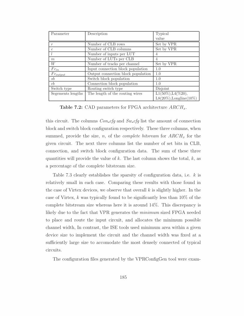
Parameter Description Typicalvalue
r Number of CLB rows Set by VPRc Number of CLB columns Set by VPRl Number of inputs per LUT 4m Number of LUTs per CLB 4W Number of tracks per channel Set by VPRFcin Input connection block population 1.0Fcoutput Output connection block population 1.0sb Switch block population 1.0cb Connection block population 1.0Switch type Routing switch type DisjointSegements lengths The length of the routing wires L1(50%),L4(%20),
L8(20%),Longline(10%)
Table 7.2: CAD parameters for FPGA architecture ARCHx.
this circuit. The columns Con cfg and Sw cfg list the amount of connection
block and switch block configuration respectively. These three columns, when
summed, provide the size, n, of the complete bitsream for ARCHx for the
given circuit. The next three columns list the number of set bits in CLB,
connection, and switch block configuration data. The sum of these three
quantities will provide the value of k. The last column shows the total, k, as
a percentage of the complete bitstream size.
Table 7.3 clearly establishes the sparsity of configuration data, i.e. k is
relatively small in each case. Comparing these results with those found in
the case of Virtex devices, we observe that overall k is slightly higher. In the
case of Virtex, k was typically found to be significantly less than 10% of the
complete bitstream size whereas here it is around 14%. This discrepancy is
likely due to the fact that VPR generates the minimum sized FPGA needed
to place and route the input circuit, and allocates the minimum possible
channel width, In contrast, the ISE tools used minimum area within a given
device size to implement the circuit and the channel width was fixed at a
sufficiently large size to accomodate the most densely connected of typical
circuits.
The configuration files generated by the VPRConfigGen tool were exam-
185

Cir
cuit
#B
LE
#C
LB
#N
ets
#R
#C
Clb
cfg
Con
cfg
Sw
cfg
Clb
kC
onk
Sw
kk
as(b
its)
(bit
s)(b
its)
(bit
s)(b
its)
(bit
s)%
ofn
alu4
1,52
238
11,
536
2020
54,8
6481
,144
40,9
5013
,749
8,79
73,
564
14.7
5ap
ex2
1,87
847
01,
916
2222
67,6
8012
0,61
262
,490
16,5
0512
,805
5,41
213
.85
apex
41,
262
316
1,27
118
1845
,504
82,3
0842
,258
14,3
248,
307
3,53
915
.39
big
key
1,70
742
71,
936
2727
61,4
8810
0,35
244
,628
12,9
477,
971
3,59
711
.87
clm
a8,
383
2,09
68,
445
4646
301,
824
592,
012
331,
722
82,2
8655
,920
25,1
7713
.33
des
1,59
139
81,
847
3232
57,3
1216
1,17
268
,934
14,9
447,
860
4,91
49.
64diff
eq1,
497
375
1,56
120
2054
,000
72,3
2433
,714
11,6
687,
591
2,64
013
.68
dsi
p1,
370
343
1,59
927
2749
,392
100,
352
44,2
5011
,041
7,31
93,
284
11.1
6el
lipti
c3,
604
901
3,73
531
3112
9,74
424
1,66
412
8,28
626
,457
21,6
088,
832
11.3
9ex
1010
4,59
81,
150
4,60
834
3416
5,60
032
8,30
018
2,55
055
,901
34,4
399,
668
14.7
8ex
5p1,
064
266
1,07
217
1738
,304
66,0
9635
,730
13,8
567,
645
3,18
817
.62
fris
c3,
556
889
3,57
630
3012
8,01
623
8,32
812
7,01
428
,691
22,4
568,
961
12.1
8m
isex
31,
397
350
1,41
119
1950
,400
76,8
0039
,972
12,5
768,
869
3,71
315
.05
pdc
4,57
51,
144
4,59
134
3416
4,73
637
2,40
021
4,22
458
,324
35,5
7113
,776
14.3
3s2
981,
931
483
1,93
522
2269
,552
90,9
8844
,628
15,7
1710
,533
3,32
814
.42
s384
176,
406
1,60
26,
435
4141
230,
688
338,
688
177,
726
52,6
6235
,596
13,2
6513
.59
s385
84.1
6,44
71,
612
6,48
541
4123
2,12
832
4,57
616
4,64
644
,386
30,3
4012
,387
12.0
8se
q1,
750
438
1,79
121
2163
,072
112,
288
58,0
8015
,701
11,8
894,
874
13.9
1sp
la3,
690
923
3,70
631
3113
2,91
227
8,52
815
4,09
845
,291
27,2
1310
,090
14.6
0ts
eng
1,04
726
21,
099
1717
37,7
2850
,544
22,5
967,
390
4,85
91,
913
12.7
7
Table
7.3
:Par
amet
ers
ofth
eben
chm
ark
circ
uit
son
AR
CH
x.
186

0
0.05
0.1
0.15
0.2
0.25
0.3
0.35
0 10 20 30 40 50 60 70 80 90 100
Pro
babi
lity
X=
i
Run size in bits (X=i)
"alu4_arch_x"
(a) Circuit alu4ARCHx
0
0.05
0.1
0.15
0.2
0.25
0.3
0.35
0 10 20 30 40 50 60 70 80 90 100P
roba
bilit
y X
=i
Run size in bits (X=i)
"des_arch_x"
(b) Circuit desARCHx
0
0.05
0.1
0.15
0.2
0.25
0.3
0.35
0 10 20 30 40 50 60 70 80 90 100
Pro
babi
lity
X=
i
Run size in bits (X=i)
"frisc_arch_x"
(c) Circuit friscARCHx
0
0.05
0.1
0.15
0.2
0.25
0.3
0 10 20 30 40 50 60 70 80 90 100
Pro
babi
lity
X=
i
Run size in bits (X=i)
"tseng_arch_x"
(d) Circuit tsengARCHx
Figure 7.11: The relationship between runsize i and P (X = i), i > 0, forfour selected circuits on ARCHx.
187

ined. Runs of zeros in each file were considered and it was found that they
follow a similar pattern to that determined for Virtex configurations (as dis-
cussed in Chapter 6). Figure 7.11 shows the distribution of the runlengths
for four selected circuits on ARCHx. The entropy of reconfiguration was
calculated assuming that the symbol set consisted of runs of zeros. Table 7.4
lists the results assuming the final bitstream was output in the three different
formats. The predicted reduction in bitstream sizes for each circuit is listed
under the column H . It can be seen that percentage reduction is highest
with format 1 even though the other two formats offer a similar value of en-
tropy. Format 1 is better than the other two because it clearly differentiates
between the configuration data of disparate resources.
In order to establish the randomness of the set bits in the VPR configura-
tions, the experiments of Section 6.2.4 were repeated. The results were found
to be similar to the Virtex case which suggests that for practical purposes,
one can consider the set bits in an FPGA configuration data to be randomly
located and can therefore apply Shannon’s formula to measure the entropy.
Table 7.4 suggests that VPR configuration can be compressed less than
the Virtex configurations. This is probably due to the higher ratio of set bits
for reasons explained above. The mean entropy of an XCV400 circuits was
found to be around 5 while in the case of Format 1 configurations of VPR it
is around 3.5. Ignoring the effect of different benchmark sets and of different
place and route tools, this result suggests that Virtex configurations contain
more information. This again can be explained by noting that circuits on a
Virtex device must take into account a fixed amount of resources as opposed
to VPR, which adds more resources as needed. However, it does not mean
that overall VPR architectures are better in terms of circuit area and delay.
This highlights the need for future research in the architecture domain where
area/time/reconfiguration-entropy are considered as three parameters of the
design space and are optimised as such. Section 7.7 and 7.8 present a few
initial experiments in this direction.
188

7.6 Compressing Configuration Data
Two compression methods were considered: vector compression and Golomb
encoding. The configuration data corresponding to the benchmark circuits
on ARCHx was examined. Vector compression was applied with various
sized blocks and at several levels. The block size was kept constant at each
level. Two levels of vector compression provided best results in all cases (i.e.
up to Level-2 vector was generated in each case). The optimal block sizes
were found to be 4 and 8. Table 7.4 shows the results for Formats 1 (F1), 2
(F2) and 3 (F3) respectively. The optimal value of the block size, b, is also
listed.
Golomb encoding was applied on the test data for various values of m. It
was found that m = 4 was optimal for most cases. Table 7.4 shows the results
for Formats 1(F1), 2 (F2) and 3 (F3) respectively. The optimal value of m
is also listed. These tables demonstrate that vector compression performs
better than Golomb encoding in almost all cases. These results show that
Format 1 allows for the best compression. Moreover, theoretically optimal
compression would gain no more than an additional 10% reduction in the
bitstream size if Format 1 is used.
7.7 The Impact of Cluster Size on Reconfig-
uration Time
This section considers a vertical subspace (see Figure 7.3) and examines a
range of alternative architectures. Configuration data for these architectures
is generated using the method described in Section 7.4. The best possible
compression for these configurations is calculated and vector compression is
applied on each set of data. The predicted results are then compared to
the actual performance of vector compression. The focus of this and the
following section is not so much on proving the validity of the configuration
189

Cir
cuit
Pre
dic
ted
Vec
tor
Addre
ssG
olom
bF1
F2
F3
F1
F2
F3
F1
F2
F3
%rd
.%
rd.
%rd
.%
rd.
b%
rd.
b%
rd.
b%
rd.
m%
rd.
m%
rd.
m
alu4
4744
4439
435
435
438
435
435
4ap
ex2
4946
4641
438
438
440
438
438
4ap
ex4
4846
4541
438
437
436
432
432
4big
key
5242
4142
830
430
445
434
434
4cl
ma
5150
5044
443
442
441
440
440
4des
5839
3955
826
426
453
830
430
4diff
eq48
4645
394
364
354
414
374
374
dsi
p57
3938
528
284
264
474
304
304
ellipti
c56
5453
494
474
464
464
444
444
ex10
1051
5150
454
444
434
374
364
364
ex5p
4439
3937
830
430
430
424
424
4fr
isc
5353
5247
446
445
444
443
443
4m
isex
346
4443
384
354
354
374
344
344
pdc
5252
5147
845
445
438
437
437
4s2
9848
4746
384
374
374
394
374
374
s384
1749
4848
424
404
404
414
394
394
s385
84.1
5352
5145
443
443
445
443
443
4se
q49
4847
414
394
394
404
384
384
spla
5149
4847
842
442
438
435
435
4ts
eng
5147
4742
436
436
443
439
439
4
Table
7.4
:R
educt
ions
inbit
stre
amsi
zes
achie
ved
usi
ng
For
mat
3.
190

Parameter Description Typicalvalue
r Number of CLB rows Set by VPRc Number of CLB columns Set by VPRl Number of inputs per LUT 4m Number of LUTs per CLB 2,4,8,16W Number of tracks per channel Set by VPRFcin Input connection block population 1.0Fcoutput Output connection block population 1.0sb Switch block population 1.0cb Connection block population 1.0Switch type Routing switch type DisjointSegements lengths The length of the routing wires L4(100%)
Table 7.5: CAD parameters for FPGA architectures ARCHCLB.
model but rather on studying the impact of the FPGA architecture (i.e.
CLB and routing architecture) on the size of the complete bitstream and the
performance of vector compression in this context.
A family of FPGAs, ARCHCLB, was specified. Table 7.5 provides details
about various parameters of the ARCHCLB subspace. The number of BLEs
per CLB were taken from the set {2,4,8,16}. Only length 4 wires were used
as other researchers have shown that this distribution produces a reasonable
balance between routability, critical delay and the area of a range of circuits
[4]. A total of four architectures was examined. As placement and routing
is a time consuming task, only the first ten circuits listed in Table 7.3 were
mapped onto each architecture. The total area needed by each instance of
FPGA (i.e. for each circuit) was recorded from the VPR output. VPR out-
puts this area in terms of the total number of minimum sized transistors
that are needed to implement the target FPGA. It should again be empha-
sised that as VPR was allowed to define the minimum sized FPGA, this area
changes from circuit to circuit. Similarly, the critical delay of each circuit
was recorded from the output of VPR. In its default operation, VPR contains
values of the transistor/wire sizes and delays that corresponds to a generic
0.35μm process.
Each architecture was considered and the arithmetic mean of all 10 FPGA
191

2.5e+06
3e+06
3.5e+06
4e+06
4.5e+06
5e+06
5.5e+06
2 4 6 8 10 12 14 16 3e-08
3.5e-08
4e-08
4.5e-08
5e-08
5.5e-08
6e-08
#Min
-siz
e tr
ansi
stor
s
Crit
ical
Del
ay (
s)
#BLEs per CLB
"L4_area""L4_time"
Figure 7.12: Mean area and delay for the benchmark circuits with variousCLB sizes. L4 signifies that Length-4 wires were used in all architectures.
areas was calculated. Similarly, the geometric mean of 10 critical delays was
calculated for each architecture (in the same manner as in [4]). Figure 7.12
plots both the mean area, measured in number of minimum sized transistors,
and the mean critical delay, measured in seconds. It can be seen that increas-
ing the CLB size increases the total area but at the same time the critical
delay of the circuit is reduced. This is a because as the CLB becomes larger,
more components of the input circuit can be packed into the logic blocks. As
the delay within a CLB is less than between CLBs, the overall critical delay
is reduced.
The configuration data for each of the 10 circuits on each of the four ar-
chitectures was output in Format 1. The final bitsream sizes, their entropies
and the results of applying vector compression were recorded and, for each
architecture, the arithmetic mean of all 10 circuits was calculated. Figure
7.13 shows the mean configuration sizes for variously sized CLBs. The min-
192

100000
150000
200000
250000
300000
350000
2 4 6 8 10 12 14 16
Con
figur
atio
n si
ze (
bits
)
#BLEs per CLB
"L4_H""L4_VA"
"L4_complete"
Figure 7.13: Mean of complete configuration sizes (L4 complete), mean ofminimum possible configuration sizes (L4 H) as predicted by the entropicmodel of configuration data and mean of vector compressed configurationsizes (L4 VA) for the benchmark circuits under various CLB sizes. L4 meansthat Length-4 wires were used in each routing channel. Format 1 was usedin all configurations.
imum possible mean configuration size, as predicted by the entropy, and the
vector compressed configuration size is also plotted in the figure.
Several observations can be made regarding Figure 7.13.
• There is a significant decrease in the complete configuration size as the
number of BLEs per CLB is increased from 2 to 8. This is expected as
more components of a circuit are packed into CLBs and the inter-CLB
connectivity is reduced. This results in lesser configuration data for
switches.
• The compression in the range 2-8 BLE/CLB is significant. This is
because for small CLBs, the router needs significant inter-CLB connec-
193

tivity and the configurations tend to have a high sparsity (i.e. smaller
values of k).
• Increasing the CLB size from 8 BLEs to 16 does not significantly impact
upon either the total bitstream size, or the compression.
• The mean of the smallest possible configuration size does not vary
significantly over a range of CLB sizes. This suggests that the mean
information content for all circuits changes little from one architecture
to another.
• Vector compression delivers reasonable compression in all cases and fol-
lows the entropy curve steadily. Note that a thorough study of Golomb
and LZSS encoding is needed to demonstrate the VA superiority over
the entire domain.
In summary, while the size of the complete bitstream is a feature of the
architecture, the size of the bitstream actually needed to configure a circuit
is less dependant on the target FPGA design. This gap can be bridged
using vector compression which is a light-weight technique that performs
well in practice. Thus, vector compression efficiently hides the artifacts of
the architecture from the user who is mainly interested in providing only as
much of configuration data as is needed by the design at hand.
7.8 The Impact of Channel Routing Archi-
tecture on Reconfiguration Time
It is difficult to parameterise the complexity of the routing architecture. More
complex routing architectures might be constructed by having several hier-
archies of wires. This means wires of several different lengths will be present
in each routing channel. In VPR, the user can vary the relative proportion
of wires of different lengths in a channel. Four architectures were specified.
194

Parameter Description Typicalvalue
r Number of CLB rows Set by VPRc Number of CLB columns Set by VPRl Number of inputs per LUT 4m Number of LUTs per CLB 4W Number of tracks per channel Set by VPRFcin Input connection block population 1.0Fcoutput Output connection block population 1.0sb Switch block population 1.0cb Connection block population 1.0Switch type Routing switch type DisjointSegements lengths The length of the routing wires L1(10%), Longline(10%)
L8(x%), L4((80-x)%)x ∈ {10, 20, 40, 60}
Table 7.6: CAD parameters for FPGA architectures ARCHswitch.
The general parameters of these are shown in Table 7.6. Each architecture
was specified with the same CLB architecture, but differed from the others
in the ratio between Length-4 and Length-8 wires. Configuration data for
each architecture was generated using the VPR/VPRConfigGen tool flow.
The output was produced in Format 1.
Figure 7.14 shows a comparison between FPGA area and circuit delay as
the fraction of Length-8 wires is increased. Overall there is an increase in
area and a decrease in critical delay.
However, varying the proportion of wire lengths has much less of an im-
pact on these parameters as varying the CLB size (compare with Figure
7.14). For example, when the number of BLEs/CLB was increased from 2 to
16, the mean area almost doubled while the mean critical delay was reduced
by more than 30%. Changing the proportion of Length-8 wires from 0.1 to
0.6 increases the area by less than 10% while the delay is reduced by less
than 15%. Figure 7.15 shows the mean configuration sizes, mean of vector
compressed configuration sizes and mean of predicted minimum configura-
tion sizes obtained using the entropic model. It can be seen that changing
the proportion of wires does not incur any significant change in either of
these quantities. A possible explanation of these results is that the propor-
195

3e+06
3.05e+06
3.1e+06
3.15e+06
3.2e+06
3.25e+06
3.3e+06
10 20 30 40 50 60 4.9e-08
5e-08
5.1e-08
5.2e-08
5.3e-08
5.4e-08
5.5e-08
5.6e-08
5.7e-08
5.8e-08
#Min
-siz
e tr
ansi
stor
s
Crit
ical
del
ay (
s)
% Length 8 wires
"HR_area""HR_time"
Figure 7.14: Mean area and delay for the benchmark circuits for variousLength-4:Length-8 wire ratios. HR signifies hierarchical routing.
tion of switch configuration for Length-8 wires is quite small compared to
the total amount of configuration. Therefore, varying the proportion of the
wires does not impact upon the configuration size or its compression to any
great degree.
7.9 Generic Configuration Architectures
The results of this chapter show that the configuration architectures that
were designed for Virtex can easily be implemented for a wider variety of
island-style FPGAs. The decompressor system presented in Chapter 6 con-
sisted of three vector address decoders. More levels of vector compression
were needed for Virtex because each Virtex device has a fixed amount of
resource and a circuit either fits onto a device of a certain size or must be
mapped onto a larger device. VPR tools, on the other hand, derive an ar-
196

100000
120000
140000
160000
180000
200000
220000
240000
260000
10 20 30 40 50 60
Con
figur
atio
n si
ze (
bits
)
% Length 8 wires
"HR_complete""HR_H"
"HR_VA"
Figure 7.15: Mean of complete configuration sizes (HR complete), mean ofminimum possible configuration sizes (HR H) and mean of vector compressedconfiguration sizes (HR VA) for the benchmark circuits under various CLBsizes. HR means hierarchical routing was employed. Format 1 was used inall configurations.
197

chitecture with minimal resources. In any case, practical devices will always
have a certain degree of constraints on device size that are possible within
an architecture family. Given a range of possible device sizes, 2 to 3 levels
of vector compression with a block size of 4 or 8 is sufficient for practical
purposes.
7.10 Conclusions
This chapter has taken the results of previous chapters and has tested them
for a wider range of circuits and architectures. This simulation study shows
that a high level of sparsity exists in typical FPGA configurations. Simple
compression techniques, such as vector compression, can compress this data
by 35%-55%. Theoretically the best compression possible would allow only
an additional 10% compression for all cases.
198

Chapter 8
Conclusion & Future Work
This thesis has examined techniques for reducing reconfiguration time of fine-
grained island-style FPGAs at their configuration data level. The approach
followed has been to reduce the amount of configuration data, through effi-
cient encoding, to accelerate reconfiguration. An attempt has been made to
gauge the information content of typical configuration data, thereby allowing
us to measure the performance of various encoding methods. In the light of
the entropic model, two simple encoding methods, namely Golomb encoding
and hierarchical vector compression, have been analysed in detail. It is shown
that both methods outperform existing methods in terms of the quality of
compression and in terms of the complexity of the compressor and the de-
compressor. Vector compression is chosen for hardware implementation due
to its superior performance and simplicity. New configuration memory ar-
chitectures have been presented that incorporate vector compression in their
hardware. It is shown that with these enhancements, a 10-fold increase in
reconfiguration speed is practical if the power dissipation is acceptable. It
is believed that the proposed methods are readily implementable in current
and future generations of SRAM-based FPGAs.
The author believes that the research reported in this thesis is not limited
to new FPGA architectures. Consider improving application-level program-
199

ming interfaces, such as JBits. Two bottlenecks can readily be identified:
1. A JBits program internally maintains a complete configuration that
is updated at runtime as directed by the program logic. This is a
memory intensive operation to which microprocessor architectures are
poorly suited.
2. JBits internally performs bit-level operations on a large amount of con-
figuration data and as such Java is not a suitable language for this
application.
An alternative proposal might be a Vector Addressed Bits (VBits) inter-
face, which internally maintains a compressed version of configuration data,
and as such all update operations are performed on the compressed data in
order to reduce the time needed to perform reconfiguration. The updated
configuration can either be decompressed in software, or in hardware, for
final upload.
FPGAs have become an important computational resources for a range of
embedded systems such as those involving software-defined radios, medical
imaging, networking, encryption, high speed scientific data acquisition and
analysis, remote and unmanned vehicles, automotive and imaging [33]. The
distinguishing feature of these applications is that they have stringent per-
formance (area/time/power) requirements. There is a performance penalty
of using an FPGA as a replacement for an ASIC [49]. However, it can be
argued that this penalty can be offset to a considerable extent by using fast
runtime reconfiguration.
The reconfiguration times of contemporary FPGAs limit their applicabil-
ity to a narrow domain of applications. Consider an XCV1000 device that
takes around 25ms to completely reconfigure. We can ignore the overhead of
reconfiguration in a particular application if the configured circuit executes
for more then 250ms. Thus, Virtex realistically allows not more than 4 useful
circuit reconfigurations per second. With a 90% reduction in reconfiguration
200

time, as has been shown in this thesis, up to 40 useful circuit reconfigurations
per second are possible. This processing rate is close to what is needed by
high quality video applications. Thus, the techniques presented in this thesis
are likely to open new avenues for deploying runtime reconfigurable FPGAs
as first class compute resources.
201

Appendix A
A Note on the Use of the Term
‘Configuration’
The term configuration in the context of Field Programmable Gate Arrays is
overloaded with different meanings. In order to clarify the discussion, various
common uses are listed below:
• The term configuration can mean a configuration state of an FPGA. For
example as in ‘the configuration of the device was changed to adapt to
the new functional requirements’.
• It can also mean configuration data that resides in the configuration
memory of an FPGA. For example as in ‘the configuration was stored
on the host machine’. Typically, a configuration in this context means a
configuration file that contains configuration data for the device under
consideration while configurations mean several configuration files.
• A third meaning of the term implies the process of loading configuration
data onto the device. For example as in ‘while the configuration was
in progress, the host continued running its applications’.
• The term partial configuration means either partial configuration data
or the process of loading partial configuration data.
202

The term reconfiguration almost always mean the process of altering the
configuration state of the device by loading new configuration data onto the
device. The term runtime or dynamic reconfiguration means reconfiguring
while the device is performing a meaningful computation from the user’s
point of view.
203

Appendix B
Detailed Results for Section 4.8
204

Circuit XCV100 XCV200 XCV300 XCV400 XCV600 XCV800 XCV1000encoder 4,230 4,302 4,421 4,394 4,168 4,312 4,320uart 5,402 5,321 5,135 5,129 5,333 5,110 5,536asyn-fifo 5,363 5,441 5,669 5,885 5,930 5,880 5,913add-sub - - 5,770 5,997 6,206 6,419 6,1552compl-1 - - 7,552 7,806 8,060 8,338 9,212spi 7,977 7,983 8,046 7,956 7,885 7,742 8,041fir-srg 8,520 8,534 8,269 8,503 7,982 8,013 8,169dfir 8,083 7,981 8,559 8,535 8,395 8,490 8,710cic3r32 8,722 9,061 8,770 9,092 8,685 9,258 8,478ccmul 9,554 9,956 9,771 9,956 10,152 9,953 10,215bin-decod - - 8,612 10,670 11,292 11,080 10,6482compl-2 - - - 11,154 11,633 12,213 12,738ammod 11,667 11,546 11,575 11,653 11,605 11,921 12,032bfproc 14,179 14,753 14,812 14,859 14,988 15,913 15,497costLUT 16,403 16,424 16,321 16,752 16,439 16,201 16,093gpio - 30,762 30,518 30,924 31,267 32,045 32,226irr - 34,830 34,927 33,648 35,397 34,119 33,506des - - - 48,118 49,226 48,255 49,827cordic - 48,759 49,484 49,364 49,327 50,072 50,202rsa - 49,179 49,989 50,121 50,782 50,710 51,283dct - 52,916 52,241 52,999 54,272 53,637 53,959blue-th - - 90,700 100,996 101,500 102,286 101,776vfft1024 - - 111,825 113,695 114,947 114,484 114,648fpu - - 134,403 155,387 157,139 154,524 155,354
Table B.1: The amount of non-null data in bits. Configuration granularity= 1 bit.
205
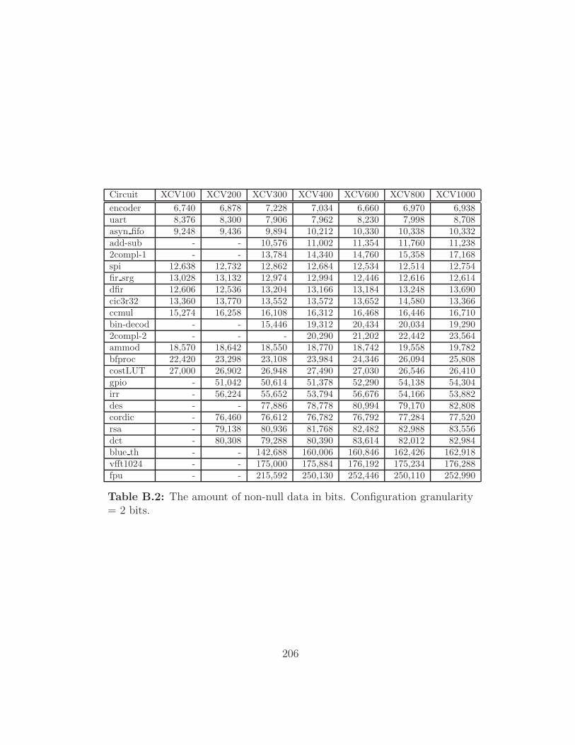
Circuit XCV100 XCV200 XCV300 XCV400 XCV600 XCV800 XCV1000encoder 6,740 6,878 7,228 7,034 6,660 6,970 6,938uart 8,376 8,300 7,906 7,962 8,230 7,998 8,708asyn fifo 9,248 9,436 9,894 10,212 10,330 10,338 10,332add-sub - - 10,576 11,002 11,354 11,760 11,2382compl-1 - - 13,784 14,340 14,760 15,358 17,168spi 12,638 12,732 12,862 12,684 12,534 12,514 12,754fir srg 13,028 13,132 12,974 12,994 12,446 12,616 12,614dfir 12,606 12,536 13,204 13,166 13,184 13,248 13,690cic3r32 13,360 13,770 13,552 13,572 13,652 14,580 13,366ccmul 15,274 16,258 16,108 16,312 16,468 16,446 16,710bin-decod - - 15,446 19,312 20,434 20,034 19,2902compl-2 - - - 20,290 21,202 22,442 23,564ammod 18,570 18,642 18,550 18,770 18,742 19,558 19,782bfproc 22,420 23,298 23,108 23,984 24,346 26,094 25,808costLUT 27,000 26,902 26,948 27,490 27,030 26,546 26,410gpio - 51,042 50,614 51,378 52,290 54,138 54,304irr - 56,224 55,652 53,794 56,676 54,166 53,882des - - 77,886 78,778 80,994 79,170 82,808cordic - 76,460 76,612 76,782 76,792 77,284 77,520rsa - 79,138 80,936 81,768 82,482 82,988 83,556dct - 80,308 79,288 80,390 83,614 82,012 82,984blue th - - 142,688 160,006 160,846 162,426 162,918vfft1024 - - 175,000 175,884 176,192 175,234 176,288fpu - - 215,592 250,130 252,446 250,110 252,990
Table B.2: The amount of non-null data in bits. Configuration granularity= 2 bits.
206

Circuit XCV100 XCV200 XCV300 XCV400 XCV600 XCV800 XCV1000encoder 12,244 12,532 13,396 12,844 12,172 12,832 12,656uart 15,304 15,084 14,320 14,540 14,928 14,584 15,900asyn-fifo 17,144 17,372 18,024 18,572 18,888 18,916 19,016add-sub - - 19,660 20,516 21,064 21,940 21,0442compl - - 25,956 26,932 27,916 28,916 32,612spi 22,996 23,292 23,356 23,408 22,828 22,900 22,944fir-srg 23,464 23,868 23,392 23,652 22,852 23,192 22,916dfir 23,172 23,000 24,256 23,936 24,100 24,216 24,892cic3r32 24,772 25,492 25,204 25,128 25,060 27,288 24,804ccmul 27,692 30,064 29,680 29,988 30,204 30,152 30,724bin-decod - - 28,892 36,000 38,280 37,640 36,2322compl-2 - - - 38,316 40,160 42,364 44,724ammod 33,824 33,876 33,796 34,384 34,492 36,116 36,548bfproc 41,056 42,420 42,168 44,028 45,272 48,312 47,912costLUT 48,676 48,388 48,880 49,740 48,480 47,864 47,372gpio - 92,448 91,724 93,724 95,084 98,716 99,380irr - 101,940 101,184 97,444 102,908 98,320 98,008des - - 141,384 143,312 147,668 144,220 152,040cordic - 137,916 137,544 137,928 138,364 139,444 139,960rsa - 141,672 144,860 146,776 147,752 148,408 149,728dct - 145,568 143,276 145,752 152,004 148,380 150,212blue-th - - - 289,568 292,224 295,540 296,836vfft1024 - - 311,440 315,512 318,516 316,672 317,692fpu - - - 450,600 455,648 453,156 458,868
Table B.3: The amount of non-null data in bits. Configuration granularity= 4 bits.
207

Circuit Virtex Frame RAM DMA VA(bits) (bits) %red. %red. %red.
encoder-xcv100 297,920 12,244 77 69 42uart-xcv100 304,192 15,304 72 62 42asyn-fifo-xvc100 498,624 17,144 81 73 64add-sub-xcv100 - - - - -2compl-1-xcv100 - - - - -spi-xcv100 417,536 22,996 70 60 56fir-srg-xcv100 203,840 23,464 37 17 9dfir-xcv100 416,192 23,172 69 57 56cic3r32-xcv100 399,616 24,772 66 52 53ccmul-xcv100 382,144 27,692 60 46 51bin-decod-xcv100 - - - - -2compl-2-xcv100 - - - - -ammod-xcv100 401,408 33,824 54 38 51bfproc-xcv100 502,208 41,056 55 39 60costLUT-xcv100 505,344 48,676 47 27 58gpio-xcv100 - - - - -irr-xcv100 - - - - -des-xcv100 - - - - -cordic-xcv100 - - - - -rsa-xcv100 - - - - -dct-xcv100 - - - - -blue-th-xcv100 - - - - -vfft1024-xcv100 - - - - -fpu-xcv100 - - - - -
Table B.4: Comparing various addressing schemes. Granularity = 4 bits.Target device = XCV100.
208
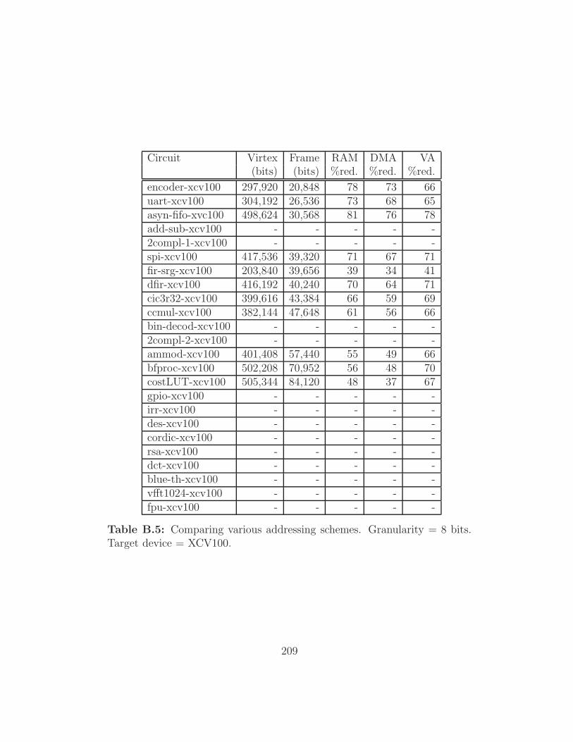
Circuit Virtex Frame RAM DMA VA(bits) (bits) %red. %red. %red.
encoder-xcv100 297,920 20,848 78 73 66uart-xcv100 304,192 26,536 73 68 65asyn-fifo-xvc100 498,624 30,568 81 76 78add-sub-xcv100 - - - - -2compl-1-xcv100 - - - - -spi-xcv100 417,536 39,320 71 67 71fir-srg-xcv100 203,840 39,656 39 34 41dfir-xcv100 416,192 40,240 70 64 71cic3r32-xcv100 399,616 43,384 66 59 69ccmul-xcv100 382,144 47,648 61 56 66bin-decod-xcv100 - - - - -2compl-2-xcv100 - - - - -ammod-xcv100 401,408 57,440 55 49 66bfproc-xcv100 502,208 70,952 56 48 70costLUT-xcv100 505,344 84,120 48 37 67gpio-xcv100 - - - - -irr-xcv100 - - - - -des-xcv100 - - - - -cordic-xcv100 - - - - -rsa-xcv100 - - - - -dct-xcv100 - - - - -blue-th-xcv100 - - - - -vfft1024-xcv100 - - - - -fpu-xcv100 - - - - -
Table B.5: Comparing various addressing schemes. Granularity = 8 bits.Target device = XCV100.
209

Circuit Virtex Frame RAM DMA VA(bits) (bits) %red. %red. %red.
encoder-xcv100 297,920 34,912 77 77 75uart-xcv100 304,192 42,496 72 73 73asyn-fifo-xvc100 498,624 51,552 79 78 82add-sub-xcv100 - - - - -2compl-1-xcv100 - - - - -spi-xcv100 417,536 62,560 70 71 75fir-srg-xcv100 203,840 61,232 40 51 50dfir-xcv100 416,192 66,400 68 70 74cic3r32-xcv100 399,616 71,264 64 70 72ccmul-xcv100 382,144 75,536 60 64 70bin-decod-xcv100 - - - - -2compl-2-xcv100 - - - - -ammod-xcv100 401,408 93,248 54 60 67bfproc-xcv100 502,208 115,088 54 60 69costLUT-xcv100 505,344 139,504 45 47 64gpio-xcv100 - - - - -irr-xcv100 - - - - -des-xcv100 - - - - -cordic-xcv100 - - - - -rsa-xcv100 - - - - -dct-xcv100 - - - - -blue-th-xcv100 - - - -vfft1024-xcv100 - - - - -fpu-xcv100 - - - - -
Table B.6: Comparing various addressing schemes. Granularity = 16 bits.Target device = XCV100.
210
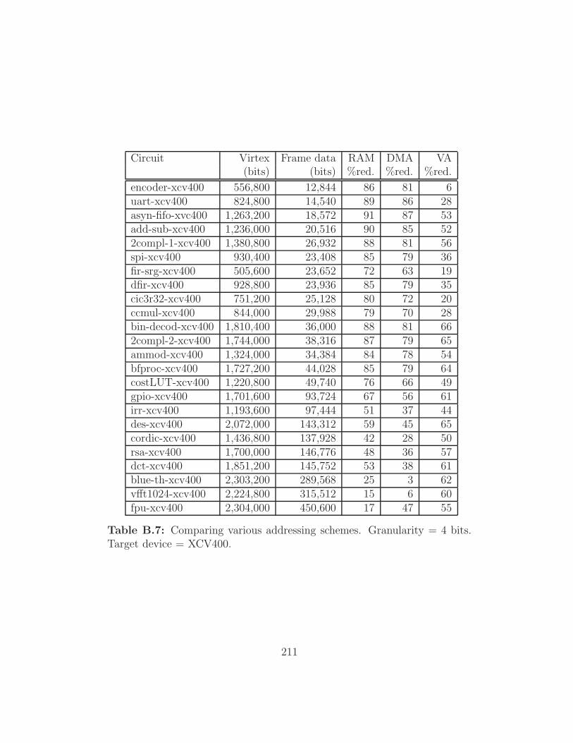
Circuit Virtex Frame data RAM DMA VA(bits) (bits) %red. %red. %red.
encoder-xcv400 556,800 12,844 86 81 6uart-xcv400 824,800 14,540 89 86 28asyn-fifo-xvc400 1,263,200 18,572 91 87 53add-sub-xcv400 1,236,000 20,516 90 85 522compl-1-xcv400 1,380,800 26,932 88 81 56spi-xcv400 930,400 23,408 85 79 36fir-srg-xcv400 505,600 23,652 72 63 19dfir-xcv400 928,800 23,936 85 79 35cic3r32-xcv400 751,200 25,128 80 72 20ccmul-xcv400 844,000 29,988 79 70 28bin-decod-xcv400 1,810,400 36,000 88 81 662compl-2-xcv400 1,744,000 38,316 87 79 65ammod-xcv400 1,324,000 34,384 84 78 54bfproc-xcv400 1,727,200 44,028 85 79 64costLUT-xcv400 1,220,800 49,740 76 66 49gpio-xcv400 1,701,600 93,724 67 56 61irr-xcv400 1,193,600 97,444 51 37 44des-xcv400 2,072,000 143,312 59 45 65cordic-xcv400 1,436,800 137,928 42 28 50rsa-xcv400 1,700,000 146,776 48 36 57dct-xcv400 1,851,200 145,752 53 38 61blue-th-xcv400 2,303,200 289,568 25 3 62vfft1024-xcv400 2,224,800 315,512 15 6 60fpu-xcv400 2,304,000 450,600 17 47 55
Table B.7: Comparing various addressing schemes. Granularity = 4 bits.Target device = XCV400.
211
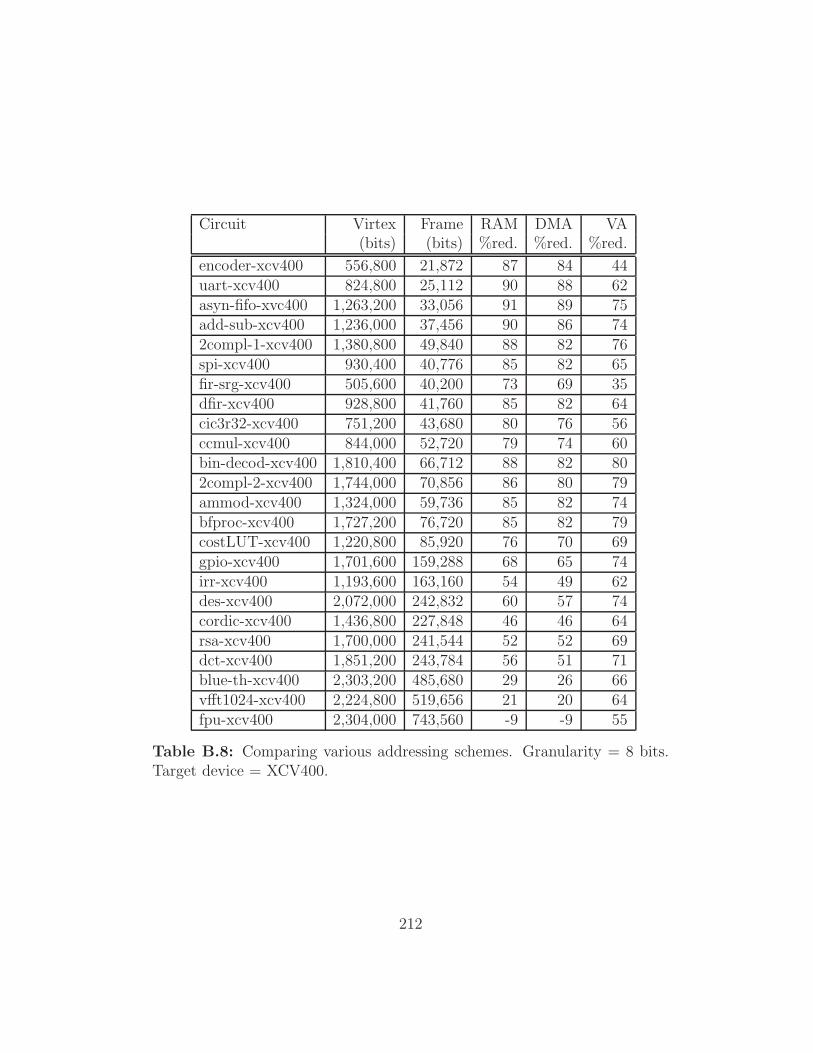
Circuit Virtex Frame RAM DMA VA(bits) (bits) %red. %red. %red.
encoder-xcv400 556,800 21,872 87 84 44uart-xcv400 824,800 25,112 90 88 62asyn-fifo-xvc400 1,263,200 33,056 91 89 75add-sub-xcv400 1,236,000 37,456 90 86 742compl-1-xcv400 1,380,800 49,840 88 82 76spi-xcv400 930,400 40,776 85 82 65fir-srg-xcv400 505,600 40,200 73 69 35dfir-xcv400 928,800 41,760 85 82 64cic3r32-xcv400 751,200 43,680 80 76 56ccmul-xcv400 844,000 52,720 79 74 60bin-decod-xcv400 1,810,400 66,712 88 82 802compl-2-xcv400 1,744,000 70,856 86 80 79ammod-xcv400 1,324,000 59,736 85 82 74bfproc-xcv400 1,727,200 76,720 85 82 79costLUT-xcv400 1,220,800 85,920 76 70 69gpio-xcv400 1,701,600 159,288 68 65 74irr-xcv400 1,193,600 163,160 54 49 62des-xcv400 2,072,000 242,832 60 57 74cordic-xcv400 1,436,800 227,848 46 46 64rsa-xcv400 1,700,000 241,544 52 52 69dct-xcv400 1,851,200 243,784 56 51 71blue-th-xcv400 2,303,200 485,680 29 26 66vfft1024-xcv400 2,224,800 519,656 21 20 64fpu-xcv400 2,304,000 743,560 -9 -9 55
Table B.8: Comparing various addressing schemes. Granularity = 8 bits.Target device = XCV400.
212

Circuit Virtex Frame RAM DMA VA(bits) (bits) %red. %red. %red.
encoder-xcv400 556,800 35,680 86 87 68uart-xcv400 824,800 41,120 89 89 78asyn-fifo-xvc400 1,263,200 55,184 91 90 84add-sub-xcv400 1,236,000 66,304 89 86 832compl-1-xcv400 1,380,800 89,568 86 84 83spi-xcv400 930,400 68,400 84 84 77fir-srg-xcv400 505,600 64,896 73 76 59dfir-xcv400 928,800 67,936 84 85 77cic3r32-xcv400 751,200 72,848 79 82 71ccmul-xcv400 844,000 86,592 78 79 73bin-decod-xcv400 1,810,400 120,880 86 83 852compl-2-xcv400 1,744,000 128,720 84 82 84ammod-xcv400 1,324,000 98,720 84 85 82bfproc-xcv400 1,727,200 127,280 84 86 84costLUT-xcv400 1,220,800 146,208 75 74 76gpio-xcv400 1,701,600 250,144 69 71 77irr-xcv400 1,193,600 255,488 55 66 67des-xcv400 2,072,000 379,888 61 67 75cordic-xcv400 1,436,800 343,872 49 62 66rsa-xcv400 1,700,000 361,008 55 63 70dct-xcv400 1,851,200 380,800 56 62 72blue-th-xcv400 2,303,200 741,776 32 44 62vfft1024-xcv400 2,224,800 785,968 25 45 58fpu-xcv400 2,304,000 1,117,472 -3 22 45
Table B.9: Comparing various addressing schemes. Granularity = 16 bits.Target device = XCV400.
213

Circuit Virtex Frame RAM DMA VA(bits) (bits) %red. %red. %red.
encoder-xcv1000 942,240 12,656 92 88 -54uart-xcv1000 1,269,216 15,900 92 89 -15asyn-fifo-xvc1000 2,275,104 19,016 95 92 36add-sub-xcv1000 2,170,272 21,044 94 90 332compl-1-xcv1000 2,422,368 32,612 92 86 39spi-xcv1000 1,683,552 22,944 91 89 13fir-srg-xcv1000 1,681,056 22,916 91 89 13dfir-xcv1000 1,166,880 24,892 87 82 -25cic3r32-xcv1000 601,536 24,804 74 64 -143ccmul-xcv1000 1,256,736 30,724 85 78 -17bin-decod-xcv1000 3,699,072 36,232 94 90 602compl-2-xcv1000 3,038,880 44,724 91 85 51ammod-xcv1000 2,914,080 36,548 92 89 49bfproc-xcv1000 3,822,624 47,912 92 88 61costLUT-xcv1000 525,408 47,372 44 24 -183gpio-xcv1000 3,523,104 99,380 82 76 56irr-xcv1000 1,981,824 98,008 69 60 23des-xcv1000 5,606,016 152,040 83 76 72cordic-xcv1000 3,043,872 139,960 71 63 48rsa-xcv1000 2,867,904 149,728 67 59 45dct-xcv1000 2,374,944 150,212 60 48 33blue-th-xcv1000 5,240,352 296,836 65 52 67vfft1024-xcv1000 3,842,592 317,692 48 34 54fpu-xcv1000 4,561,440 458,868 37 19 58
Table B.10: Comparing various addressing schemes. Granularity = 4 bits.Target device = XCV1000.
214
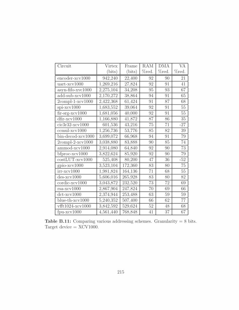
Circuit Virtex Frame RAM DMA VA(bits) (bits) %red. %red. %red.
encoder-xcv1000 942,240 22,400 92 90 21uart-xcv1000 1,269,216 27,824 92 91 41asyn-fifo-xvc1000 2,275,104 34,208 95 93 67add-sub-xcv1000 2,170,272 38,864 94 91 652compl-1-xcv1000 2,422,368 61,424 91 87 68spi-xcv1000 1,683,552 39,064 92 91 55fir-srg-xcv1000 1,681,056 40,000 92 91 55dfir-xcv1000 1,166,880 41,872 87 86 35cic3r32-xcv1000 601,536 43,216 75 71 -27ccmul-xcv1000 1,256,736 53,776 85 82 39bin-decod-xcv1000 3,699,072 66,968 94 91 792compl-2-xcv1000 3,038,880 83,888 90 85 74ammod-xcv1000 2,914,080 64,840 92 90 73bfproc-xcv1000 3,822,624 85,920 92 90 79costLUT-xcv1000 525,408 80,200 47 36 -52gpio-xcv1000 3,523,104 172,360 83 80 75irr-xcv1000 1,981,824 164,136 71 68 55des-xcv1000 5,606,016 265,928 83 80 82cordic-xcv1000 3,043,872 232,520 73 72 69rsa-xcv1000 2,867,904 247,824 70 69 66dct-xcv1000 2,374,944 253,488 63 59 59blue-th-xcv1000 5,240,352 507,400 66 62 77vfft1024-xcv1000 3,842,592 529,624 52 48 68fpu-xcv1000 4,561,440 768,848 41 37 67
Table B.11: Comparing various addressing schemes. Granularity = 8 bits.Target device = XCV1000.
215

Circuit Virtex Frame RAM DMA VA(bits) (bits) %red. %red. %red.
encoder-xcv1000 942,240 36,416 92 91 58uart-xcv1000 1,269,216 45,392 92 92 68asyn-fifo-xvc1000 2,275,104 58,480 94 93 82add-sub-xcv1000 2,170,272 70,192 93 92 802compl-1-xcv1000 2,422,368 114,000 90 88 80spi-xcv1000 1,683,552 62,144 92 92 75fir-srg-xcv1000 1,681,056 65,776 91 92 75dfir-xcv1000 1,166,880 67,008 87 89 63cic3r32-xcv1000 601,536 69,488 75 79 29ccmul-xcv1000 1,256,736 88,192 85 85 64bin-decod-xcv1000 3,699,072 121,952 93 91 872compl-2-xcv1000 3,038,880 155,392 89 86 83ammod-xcv1000 2,914,080 111,552 92 92 84bfproc-xcv1000 3,822,624 148,864 91 92 87costLUT-xcv1000 525,408 131,040 45 52 7gpio-xcv1000 3,523,104 278,256 83 83 82irr-xcv1000 1,981,824 259,072 71 78 69des-xcv1000 5,606,016 447,584 83 83 86cordic-xcv1000 3,043,872 354,320 75 80 77rsa-xcv1000 2,867,904 376,096 71 76 74dct-xcv1000 2,374,944 399,760 63 67 68blue-th-xcv1000 5,240,352 799,584 67 70 78vfft1024-xcv1000 3,842,592 816,528 54 64 69fpu-xcv1000 4,561,440 1,181,776 43 54 66
Table B.12: Comparing various addressing schemes. Granularity = 16 bits.Target device = XCV1000.
216

Appendix C
Simulating ARCH-III
This section details the method used to simulate the operation of ARCH-III.
The goal of this method is to determine the time needed to load an input
configuration under various port sizes. ARCH-III has a port size of 8p bits
where p is a non-zero integer. In an ideal architecture, increasing p should
decrease the reconfiguration time by a factor of p. However, various VADs
in ARCH-III will stall due to contention over the configuration bus. Adding
the null bypass to the design can also result in contention over the DF-Bus.
Extra pad data must therefore be inserted into the configuration bitstream
to account for these waits. The procedure described in this section calculates
this overhead. We first consider the case where the null bypass is not present
and we only need to stall for the C-bus.
In order to simplify the simulation procedure, the steps needed to load
the controller commands and the block addresses are ignored. Moreover, it is
assumed that no null blocks are specified. In other words, only user blocks are
examined. The input blocks are partitioned evenly among the p configuration
ports in case there are less than p user blocks in the φ′ configuration under
test. As the block addresses are ignored, the simulation is oblivious to the
boundaries between the blocks. It considers all frames that are assigned to
ith V ADi as a list where 0 ≤ i ≤ p−1. The input to the simulation procedure
217
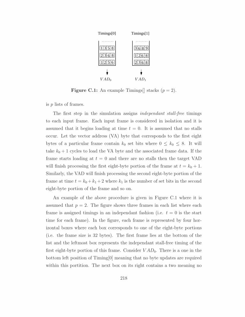
Timings[0] Timings[1]
1 2 5 6
2 3 6 8
1 3 5 8
2 3 6 8
1 2 6 8
3 6 8 9
V AD0 V AD1
Figure C.1: An example Timings[] stacks (p = 2).
is p lists of frames.
The first step in the simulation assigns independant stall-free timings
to each input frame. Each input frame is considered in isolation and it is
assumed that it begins loading at time t = 0. It is assumed that no stalls
occur. Let the vector address (VA) byte that corresponds to the first eight
bytes of a particular frame contain k0 set bits where 0 ≤ k0 ≤ 8. It will
take k0 + 1 cycles to load the VA byte and the associated frame data. If the
frame starts loading at t = 0 and there are no stalls then the target VAD
will finish processing the first eight-byte portion of the frame at t = k0 + 1.
Similarly, the VAD will finish processing the second eight-byte portion of the
frame at time t = k0 +k1 +2 where k1 is the number of set bits in the second
eight-byte portion of the frame and so on.
An example of the above procedure is given in Figure C.1 where it is
assumed that p = 2. The figure shows three frames in each list where each
frame is assigned timings in an independant fashion (i.e. t = 0 is the start
time for each frame). In the figure, each frame is represented by four hor-
izontal boxes where each box corresponds to one of the eight-byte portions
(i.e. the frame size is 32 bytes). The first frame lies at the bottom of the
list and the leftmost box represents the independant stall-free timing of the
first eight-byte portion of this frame. Consider V AD0. There is a one in the
bottom left position of Timing[0] meaning that no byte updates are required
within this portition. The next box on its right contains a two meaning no
218

update is required within this portion of the frame either. After this, how-
ever, two frame bytes are to be updated that will finish loading at t = 5.
The entire frame is processed at t = 6. At this stage, the mask bytes are not
considered.
The next step of the simulation updates the timing integers, that are
assigned to each frame in the first step, by considering the times at which
more then one VAD will require an access to the C-bus in order to transfer the
frame and the mask bytes. The procedure iterates over all lists one by one.
At each iteration it pops the leftmost timing integer and examines whether
this time clashes with the other VADs. If it does then this timing integer is
changed into the smallest integer that does not clash with the others in the
bottommost frame of each list. Note that two cycles of the C-bus are needed
by each VAD; one to transfer the frame bytes and the other to transfer the
mask data. All subsequent timing integers are considered in the light of this
update. The finish time of the bottommost frame in each list is determined in
this fashion. If the last integer clashes with some other integer then it means
that there is contention over the DF-bus. The finish time of this frame is
updated by giving it the smallest integer than does not clash with the finish
times of the other bottommost frames.
In the next step, the finish time for the bottommost frame is then consid-
ered as a start time of the next frame and the bottommost frame is evicted
from the list. The start time of the second frame is then added to each tim-
ing integer in the second frame. The second step is repeated to calculate the
finish time of the new frame and the procedure iterates until all frames are
processed. The maximum of all finish times is taken to be the time required
by ARCH-III to load the configuration under test.
The second step of the simulation is explained with the help of Figure C.2.
A cache is maintained to perform quick comparisons. The leftmost integer
from the bottommost frame in Timings[0] is evicted and is put in the cache.
The leftmost integer from the bottommost frame in Timing[1] is then evicted
and is compared with the contents of the cache. This comparsion also takes
219

into account the extra cycle needed for the mask byte. Since there is a 1 in
the cache, it means that the C-bus is busy at time t=2 as well. Thus, the first
available slot, which is t=3, is allocated to Timings[1]. The procedure then
considers the Timings[0] again (step-2). Since the t=2 is already used (note
the presence of a 1 in the cache), it means that there is a clash. The number
is incremented to 5 (the smallest integer with no clash) and is added to the
cache. Step-3 repeats this procedure. The numbers upto 5 are evicted from
the cache as 6 and 8 are greater then all of these. This step is necessary to
keep the cache size small. The finish times for the first frame in Timings[0]
and Timings[1] are 13 and 15 respectively. These integers are then added
to each integer in the respective next frame of the list and the procedure
iterates.
220
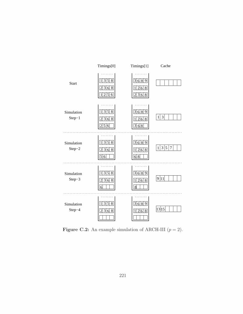
1 2 5 6 2 3 6 8
Timings[0] Timings[1]
Start
Cache
2 3 6 8
1 3 5 8
1 2 6 8
3 6 8 9Simulation
Step−3
6 8
2 3 6 8
1 3 5 8
1 2 6 8
3 6 8 9Simulation
Step−2
5 6 6 8
1 3 5
2 3 6 8
1 3 5 8
1 2 6 8
3 6 8 9
2 5 6 3 6 8
Simulation
Step−1 3
2 3 6 8
1 3 5 8
1 2 6 8
3 6 8 9
9
2 3 6 8
1 3 5 8
1 2 6 8
3 6 8 9Simulation
Step−4
1
7
11
13 15
Figure C.2: An example simulation of ARCH-III (p = 2).
221
Bibliography
[1] A. Ahmadinia, C. Bobda, H. Kalte, D. Koch, and J. Teich. FPGA ar-
chitecture extensions for preemptive multitasking and hardware defrag-
mentation. In IEEE International Conference on Field-Programmable
Technology, pages 433–436, 2004.
[2] A. Ahmadinia, C. Bobda, and J. Teich. A dynamic scheduling and
placement algorithm for reconfigurable hardware. In Organic and Per-
vasive Computing-International Conference on Architecture of Com-
puting Systems, pages 125–139, 2004.
[3] P. Bellows and B. Hutchings. JHDL–An HDL for reconfigurable sys-
tems. In IEEE Symposium on Field-Programmable Custom Computing
Machines, pages 175–184, 1998.
[4] V. Betz, J. Rose, and A. Marquardt. Architectures and CAD for Deep-
Submicron FPGAs. Kluwer Academic Publishers, 2000.
[5] B. Blodget, S. McMillan, and P. Lysaght. A lightweight approach for
embedded reconfiguration of FPGAs. In Design Automation and Test
in Europe, pages 10399–10401, 2003.
[6] C. Bobda, M. Majer, A. Ahmadinia, T. Heller, A. Linrath, J. Teich,
S.P. Fekete, and J. Veen. The Erlangen Slot Machine: A highly flexible
FPGA-based reconfiguration platform. In IEEE Symposium for Field-
Programmable Custom Computing Machines, pages 319–320, 2005.
222

[7] G. Brebner. A virtual hardware operating system for Xilinx XC6200.
In International Conference on Field-Programmable Logic and Appli-
cations, pages 327–336, 1996.
[8] G. Brebner. The Swappable Logic Unit: A paradigm for virtual hard-
ware. In IEEE Symposium on Field-Programmable Custom Computing
Machines, pages 77–86, 1997.
[9] G. Brebner and O. Diessel. Chip-based reconfigurable task manage-
ment. In International Conference on Field-Programmable Logic and
Applications, pages 182–191, 2001.
[10] G. Brebner and A. Donlin. Runtime reconfigurable routing. In Recon-
figurable Architectures Workshop, pages 25–30, 1998.
[11] J. Brown, D. Chen, I. Eslick, E. Tau, and A. Dehon. Delta: Prototype
for a first-generation dynamically programmable gate array. Transit
Tech Report 112, MIT, 1994.
[12] A. Chandra and K. Chakrabarty. System-on-a-chip test-data compres-
sion and decompression architectures based on Golomb codes. IEEE
Transactions on Computer-Aided Design of Integrated Circuits and
Systems, 20(3):113–120, 2001.
[13] P. Y.K Cheung and W. Luk. Static and dynamic reconfigurable designs
for 2D shape-adaptive DCT. In International Conference on Field-
Programmable Logic and Applications, pages 96–105, 2000.
[14] Y. Choueka, A.S. Fraenkel, S.T. Klein, and E. Segal. Improved hier-
archical bit-vector compression in document retrieval systems. In An-
nual ACM Conference on Research and Development in Information
Retrieval, pages 88–96, 1986.
[15] M.M. Chu. Dynamic runtime schedular for SCORE. Master’s thesis,
University of California Berkely, Electrical Engineering and Computer
Science Department, 2002.
223
[16] K. Compton. Programming architectures for run-time reconfigurable
systems Northwestern University, Electrical and Computer Engineering
Department, USA. Master’s thesis, 1999.
[17] K. Compton, Z. Li, J. Cooley, S. Knol, and S. Hauck. Configuration
relocation and defragmentation for run-time reconfigurable computing.
IEEE Transactions on VLSI Systems, 10(3):209–220, 2002.
[18] J. Cong and Y. Ding. Flowmap: An optimal technology mapping
algorithm for delay optimization in Lookup-Table based FPGA designs.
IEEE Transactions on Computer Aided Design, 13(1):1 – 13, 1994.
[19] A. Dandalis and V.K. Prasanna. Space-efficient mapping of 2D-DCT
onto dynamically configurable coarse-grained architectures. In Inter-
national Conference on Field-Programmable Logic and Applications,
pages 471–475, 1998.
[20] A. Dandalis and V.K. Prasanna. Configuration compression for FPGA-
based embedded systems. In International Symposium on Field -
Programmable Gate Arrays, pages 187–195, 2001.
[21] K. Danne and M. Platzner. Periodic real-time scheduling of FPGA
computers. In International Conference on Field-Programmable Logic
and Applications, pages 117–127, 2005.
[22] I.L. David, D.H Rhett, and P.M. Athanas. Framework for architecture-
independent run-time reconfigurable applications. Reconfigurable Tech-
nology: FPGAs for Computing and Applications, 4212(2):162–172,
2000.
[23] A. DeHon. Reconfigurable architectures for general-purpose computing
Technical Report 1586, MIT Artificial Intelligence Laboratory. 1996.
[24] A. Derbyshire and W. Luk. Compiling run-time parametrisable designs.
In International Conference on Field-Programmable Technology, pages
44–51, 2002.
224

[25] D. Deshphande, A.K. Somani, and A. Tyagi. Configuration scheduling
schemes for stripped FPGAs. In International Symposium on Field-
Programmable Gate Arrays, pages 206–214, 1999.
[26] J. Detrey and O. Diessel. SCCircal: A static compiler mapping XCircal
to Virtex FPGAs. Technical Report 213, University of New South
Wales, 2002.
[27] O. Diessel and H. ElGindy. Run-time compaction of FPGA designs.
In International Conference on Field-Programmable Logic and Appli-
cations, pages 131–140, 1997.
[28] O. Diessel and H. ElGindy. On scheduling dynamic FPGA reconfigura-
tions. In Australasian Conference on Parallel and Real-Time Systems,
pages 191–200, 1998.
[29] O. Diessel and U. Malik. An FPGA interpreter with virtual hardware
management. In Reconfigurable Architectures Workshop, 2002.
[30] O. Diessel and G. Milne. A hardware compiler realizing concurrent
processes in reconfigurable logic. In IEE Proceedings–Computers and
Digital Techniques, pages 152 – 162, 2001.
[31] O.D. Fidanci, D.S. Poznanovic, K. Gaj, T.A. El-Ghazawi, and N.A.
Alexandridis. Performance and overhead in a reconfigurable computer.
In Reconfigurable Architectures Workshop, page 176, 2003.
[32] M. Frances and A. Litman. On covering problem of codes. Theory of
Computing systems, 30(2):113–119, 1997.
[33] P. Garcia, K. Compton, M. Schulte, E. Blem, and W. Fu. An overview
of reconfigurable hardware in embedded systems. EURASIP Journal
of Embedded Systems, 2006.
225

[34] S. Guo and W. Luk. Compiling Ruby into FPGAs. In International
Conference on Field-Programmable Logic and Applications, pages 188–
197, 1995.
[35] R. Hartenstein. Coarse-grained architectures. In International Con-
ference on Field-Programmable Logic and Applications, pages 471–475,
1998.
[36] S. Hauck, T.W. Fry, M.M. Hosler, and J.P. Kao. The Chimaera recon-
figurable functional unit. In IEEE Symposium on Field-Programmable
Custom Computing Machines, pages 87–96, 1997.
[37] S. Hauck, Z. Li, and E.J. Schwabe. Configuration compression for the
Xilinx XC6200 FPGA. IEEE Transactions on Computer Aided Design
on Integrated, Circuits and Systems, 18(8):1237–1248, 1999.
[38] S. Hauck and W.D. Wilson. Runlength compression techniques for
FPGA configurations. Tech report, Northwestern University, Depart-
ment of Electrical and Computer Engineering, 1999.
[39] G. Haug and W. Rosentiel. Reconfigurable hardware as shared re-
source in multipurpose computers. In International Conference on
Field-Programmable Logic and Applications, pages 149–158, 1998.
[40] J.R. Hauser and J. Wawrzynek. Garp: A MIPS processor with a re-
configurable coprocessor,. In IEEE Symposium on Field-Programmable
Custom Computing Machines, pages 12–21, 1997.
[41] J. Heron and R.F. Woods. Architectural strategies for implementing
image processing algorithms on an XC6200 FPGA. In Internatioanl
Conference on Field-Programmable Logic and Applications, pages 174–
184, 1996.
[42] E. Horta and J.W. Lockwood. Parbit: A tool to transform bitfiles to
implement partial reconfiguration of Field-Programmable Gate Arrays.
Technical Report WUC-01-13, Washington University, 2001.
226
[43] M. Huebner, M. Ullmann, F. Weissel, and J. Becker. Real-time con-
figuration code decompression for dynamic FPGA self-reconfiguration.
In Reconfigurable Architectures Workshop, page 138, 2004.
[44] N. Kasprzyk, J.C. Veen, and A. Koch. Configuration merging for
adaptive computer applications. In International Conference on Field-
Programmable Logic and Applications, pages 217–222, 1995.
[45] E. Keller. JRoute: A run-time routing API for FPGA hardware. In
Reconfigurable Architecturtes Workshop, pages 874–881, 2000.
[46] I. Kennedy. Exploiting redundancy to speedup reconfiguration of an
FPGA. In International Conference on Field-Programmable Logic and
Applications, pages 262–271, 2003.
[47] S. Knap. Constant-coefficient multipliers save FPGA space, time. In
Personal Engineering, pages 45–48, July 1998.
[48] D. Kock and J. Teich. Platform-independent methodology for partial
reconfiguration. In International Conference on Computing Frontiers,
pages 398–403, 2004.
[49] I. Kuon and J. Rose. Measuring the gap between FPGAs and ASICs.
In IEEE Symposium on Field-Programmable Custom Computing Ma-
chines, 2006.
[50] S. Lange and M. Middendorf. Hyperreconfigurable architectures for fast
run time reconfiguration. In IEEE Symposium on Field-Programmable
Custom Computing Machines, pages 304–305, 2004.
[51] G. Lemieux and D. Lewis. Design of Interconnection Networks for
Programmable Logic. Kluwer Academic Publishers, 2004.
[52] Z. Li, K. Compton, and S. Hauck. Configuration cache management
techniques for FPGAs. In IEEE Symposium on Field-Programmable
Custom Computing Machines, pages 22–36, 2000.
227

[53] Z. Li and S. Hauck. Configuration compression for Virtex FPGAs.
In IEEE Symposium on Field-Programmable Custom Computing Ma-
chines, pages 147–159, 2001.
[54] Z. Li and S. Hauck. Configuration prefetching techniques for a partial
reconfigurable coprocessor with relocation and defragmentation. In
International Symposium on Field-Programmable Gate Arrays, pages
187–195, 2002.
[55] W. Luk and S. McKeever. Pebble: A language for parametrised and
reconfigurable hardware design. In Field-Programmable Logic and Ap-
plications, pages 9–18, 1998.
[56] W. Luk, N. Shirazi, and P.Y.K. Cheung. Modelling and optimis-
ing run-time reconfigurable systems. In IEEE Symposium on Field-
Programmable Custom Computing Machines, pages 167–176, 1996.
[57] W. Luk, N. Shirazi, and P.Y.K. Cheung. Compilation tools for run-time
reconfigurable designs,. In IEEE Symposium on Field-Programmable
Custom Computing Machines, pages 56 –65, 1997.
[58] P. Lysaght and J. Stockwood. A simulation tool for dynamically re-
configurable Field-Programmable Gate Arrays. IEEE Transactions on
VLSI Systems, 4(3):381–390, 1996.
[59] J. MacBeth and P. Lysaght. Dynamically reconfigurable cores. In In-
ternatioanl Conference on Field-Programmable Logic and Applications,
pages 462–472, 2001.
[60] U. Malik and O. Diessel. On the placement and granularity of
FPGA configurations. In IEEE International Conference on Field-
Programmable Technology, pages 161–168, 2004.
[61] U. Malik and O. Diessel. A configuration memory architecture for fast
Run-time reconfiguration of FPGAs. In International Conference on
Field-Programmable Logic and Applications, pages 636–639, 2005.
228

[62] U. Malik and O. Diessel. The entropy of FPGA reconfiguration. In In-
ternatioanl Conference on Field-Programmable Logic and Applications,
2006.
[63] U. Malik, K. So, and O. Diessel. Resource-aware run-time elaboration
of behavioural FPGA specifications. In IEEE International Conference
on Field-Programmable Technology, pages 68–75, 2002.
[64] G. Marsaglia. DIEHARD battery of tests of randomness v0.2 beta.
2005. http://www.csis.hku.hk/%7Ediehard/.
[65] B.G. Maya and M.S. Janice. NAPA C: Compiling for a hy-
brid RISC/FPGA architecture. In IEEE Symposium on Field-
Programmable Custom Computing Machines, pages 126–136, 1998.
[66] O. Mencer, M. Morf, and M.J. Flyn. PAM-Blox: High performance
FPGA design for adaptive computing. In IEEE Symposium on Field-
Programmable Custom Computing Machines, pages 167–174, 1998.
[67] P. Merino, J.C. Lopez, and M. Jacome. A hardware operating system
for dynamic reconfiguration of FPGAs. In International Conference on
Field-Programmable Logic and Applications, pages 591–602, 1998.
[68] U. Meyer-Baese. Digital signal processing with Field Programmable
Gate Arrays. Springer, 2001.
[69] G. Milne. A model for dynamic adaptation in reconfigurable hardware
systems. In NASA/DoD Workshop on Evolvable Hardware, pages 161–
169, 1999.
[70] E. Moscu, K. Bertels, and S. Vassiliadis. Instruction scheduling for
dynamic hardware configurations. In Design Automation and Test in
Europe, pages 100–105, 2005.
229

[71] J.H. Pan, T. Mitra, and W. Wong. Configuration bitstream compres-
sion for dynamically reconfigurable FPGAs. In International Confer-
ence on Computer Aided Design, pages 766–773, 2004.
[72] S. Park and W. Burleson. Configuration cloning: Exploiting regularity
in dynamic DSP architectures. In International Symposium on Field-
Programmable Gate Arrays, pages 81–89, 1999.
[73] P. Rau, A.V. Ghia, and S.M. Menon. Configuration memory archi-
tecture of an FPGA, United States Patent 6,501,677. Assignee: Xilinx
Inc. 2002.
[74] A.B. Ray and P.M. Athanas. Wormhole run-time reconfiguration. In
International Symposium on Field-Programmable Gate Arrays, pages
79–85, 1997.
[75] M. Richmond. A Lemple-Ziv based configuration management archi-
tecture for reconfigurable computing M.S. Thesis. University of Wash-
ington, Department of Electrical Engineering, USA. 2001.
[76] P.J Roxby and S. Guccione. Automated extraction of run-time
parametrisable cores from programmable device configurations. In
IEEE Symposium on Field-Programmable Custom Computing Ma-
chines, pages 153–161, 2000.
[77] E. J. Schwabe S. Hauck, Z. Li. Configuration compression for the Xilinx
XC6200 FPGA. Transactions on Computer-Aided Design of Integrated
Circuits and Systems, 8(1):1107–1113, 1999.
[78] S. Sadhir, S. Nath, and S.C. Goldstein. Configuration caching and
swapping. In International Conference on Field-Programmable Logic
and Applications, pages 192–202, 2001.
[79] K. Sayood. Lossless compression handbook. Academic Press, 2003.
230
[80] H. Schmit. Incremental reconfiguration for pipelined applications.
In IEEE Symposium on Field-Programmable Custom Computing Ma-
chines, pages 47–55, 1997.
[81] D.P. Schultz, S.P. Young, and L.C. Hung. Method and structure for
reading, modifying and writing selected configuration memory cells of
an FPGA, United States Patent 6,255,848. Assignee: Xilinx Inc. 2001.
[82] E. M. Sentovich. SIS: A system for sequential circuit analysis Tech. Re-
port No. UCB/ERL M92/41, University of California, Berkeley. 1992.
[83] C. Shannon. A mathematical theory of communication. Bell Systems
Technical Journal, pages 379–423, 1948.
[84] N. Shirazi, W. Luk, and P. Cheung. Runtime management of dynam-
ically reconfigurable designs. In International Conference on Field-
Programmable Logic and Applications, pages 59–68, 1998.
[85] N. Shirazi, W. Luk, and P.Y.K. Cheung. Framework and tools for run-
time reconfigurable designs. IEE Proceedings Computers and Digitial
Design Techniques, 147(3):147–152, 2000.
[86] R.P. Sidhu, A. Mei, and V.K. Prasanna. String matching on multi-
context FPGAs using self-reconfiguration. In International Symposium
on Field-Programmable Gate Arrays, pages 217 – 226, 1999.
[87] H. Simmler, L. Levinson, and R. Manner. Multitasking on FPGA co-
processors. In International Conference on Field-Programmable Logic
and Applications, pages 121–130, 2000.
[88] K. So. Compiling abstract behaviours on FPGAs. Undergraduate the-
sis. School of Computer Science and Engineering, University of New
South Wales, Sydney, Australia. 2002.
[89] J.A. Storer and T.G. Szymanski. Data compression via textual substi-
tution. Journal of ACM, 29:928–951, 1982.
231
[90] A. Takayama, Y. Shibata, K. Iwai, and H. Amano. Dataflow parti-
tioning and scheduling algortihms for WASMII, a virtual hardware.
In International Conference on Field-Programmable Logic and Appli-
cations, pages 685–694, FPL00.
[91] D. Taylor, J. Turner, and J. Lockwood. Dynamic hardware plugins
(DHP): Exploiting reconfigurable hardware for high-performance pro-
grammable routers. In IEEE Open Architectures and Network Pro-
gramming, pages 25–34, 2001.
[92] M.D. Torre, U. Malik, and O. Diessel. A configuration memory archi-
tecture supporting fast bit-stream compression for FPGAs. In Asia-
Pacific Conference on Computer Systems Architecture, pages 415–428,
2005.
[93] S. Trimberger. Scheduling designs into a time-multiplexed FPGA. In
International Symposium on Field-Programmable Gate Arrays, pages
153–160, 1998.
[94] S. Trimberger, D. Carberry, A. Johnson, and J. Wong. A time-
multiplexed FPGA. In IEEE Symposium on Field-Programmable Cus-
tom Computing Machines, pages 22–28, 1997.
[95] M. Vasilko and D. Ait-Boudaoud. Scheduling for dynamically reconfig-
urable FPGAs. In International Workshop on Logic and Architecture
Synthesis, pages 328–336, 1995.
[96] H. Walder and M. Platzner. Reconfigurable hardware operating sys-
tems: From design concepts to realizations. In International Confer-
ence on Engineering of Reconfigurable Systems and Architectures, pages
284–287, 2003.
[97] T. A. Welch. A technique for high-performance data compression.
Computer, 17:8–19, 1984.
232

[98] G.B. Wigley and D.A. Kearney. The management of applications for
runtime reconfigurable computing using an operating system. In Aus-
tralian Conference in Research and Practice in Information Technology,
pages 73–81, 2002.
[99] R.F. Woods, D.W. Trainor, and J. Heron. Applying an XC6200 to real-
time image processing. IEEE Design and Test of Computers, 15(1):30–
38, 1998.
[100] S. Yang. Logic synthesis and optimization benchmarks. Tech. report
Version 3.0, Microelectronics center of North Carolina, 1991.
[101] J. Ziv and A. Lempel. A universal algorithm for sequential data com-
pression. IEEE Transactions on Information Theory, 23(3):337–343,
1977.
[102] J. Ziv and A. Lempel. Compression of individual sequences via variable-
rate coding. IEEE Transactions on Information Theory, 24(5):530–536,
1978.
[103] Adobe photoshop Version 6.0. Adobe Inc., 2004.
[104] AT40K Field Programmable Gate Arrays datasheet. Atmel, Inc., 2004.
[105] Berkeley logic interchange format (BLIF).
http://www.bdd-portal.org/docu/blif/blif.html.
[106] DK1 design suite. Celoxica Limited, 2006.
[107] RC1000 hardware reference manual, Version 2.3. Celoxica Limited,
2001.
[108] RC1000 software reference manual, Version 1.3. Celoxica, Limited,
2001.
[109] Synopsys Design Compiler, v2004.06. Synopsys Inc., 2004.
233

[110] Dynamically reconfigurable processor (DRP). NEC Electronics, 2001.
[111] The Gecko project. Interuniversity Micorelectronics Center (IMEC,
Belgium) www.imec.be.
[112] ORCA Series 4 FPGAs datasheet. Lattice semiconductor Inc., 2003.
[113] List of FPGA-based computing machines.
http://www.io.com/~guccione/HW_list.html.
[114] Matlab Version 7.0. MathWorks Inc., 2004.
[115] Modelsim SE datasheet. Mentor Graphics, Inc., 2005.
[116] HDL Designer. Mentor Graphics Inc., 2002.
[117] Open cores Inc. www.opencores.org.
[118] TSMC 90nm core library. Taiwan Semiconductor Manufacturing Com-
pany Ltd., 2003.
[119] TVPack/VPR Manual (Version 4.30).
http://www.eecg.toronto.edu/~vaughn/vpr/vpr.html.
[120] ISE Version 5.2. Xilinx Inc., 2002.
[121] JBits SDK. Xilinx, Inc., 2000.
[122] System Ace: Configuration solution for Xilinx FPGAs, Version1.0. Xil-
inx Inc., 2001.
[123] Virtex 2.5V Field Programmable Gate Arrays Datasheet, Version 1.3.
Xilinx, Inc., 2000.
[124] Virtex-4 Field Programmable Gate Arrays Datasheet. Xilinx, Inc.,
2005.
[125] Virtex-II Field Programmable Gate Arrays Datasheet. Xilinx, Inc.,
2004.
234

[126] Virtex-II Pro Platform FPGAs Datasheet Version 1.10. Xilinx, Inc.,
2004.
[127] XC4000 XLA/XV Field-Programmable Gate Arrays Datasheet, Ver-
sion 1.3. Xilinx Inc., 1999.
[128] XC6200 Field Programmable Gate Arrays, Version 1.10. Xilinx, Inc.,
1997.
[129] Virtex Configuration Guide, Version 1.3. Xilinx, Inc., 2000.
[130] High performance, low area, interpolator design for the XC6200. Xilinx
Application note, XAPP 081 (v1.0), 1997.
235