conducting antireflection coatings with low polarization...
TRANSCRIPT

Conducting antireflection coatings with low
polarization dependent loss for
telecommunication applications
J. A. Dobrowolski1, Joseph E. Ford
2, Brian T. Sullivan
3, Liping Lu
3, and Norman R.
Osborne3
1Institute for Microstructural Sciences, National Research Council of Canada, Ottawa, Ontario, Canada K1A 0R6. 2Electrical & Computer Engineering Department, University of California San Diego, 9500 Gilman Drive, La Jolla,
CA 92093-0407 3Iridian Spectral Technologies, 1500 Montreal Road, Ottawa, Ontario K1A 0R6
[email protected], [email protected], [email protected]
Abstract: Conducting optical coatings for the visible light range are
commonly made of Indium Tin Oxide (ITO), but ITO is unsuitable for near-
infrared telecommunications wavelengths because it can become absorptive
after extended illumination. In this paper we show an alternative approach
which uses conventional coating materials to create either non-conducting
or conducting antireflection (AR) coatings that are effective over a fairly
broad spectral region (λlong/λshort ≈ 1.40) and also usable for a wide range of
angles of incidence (0-38º, or 0-55º) in the telecom wavelength range. Not
only is the transmittance of windows treated with such coatings quite high,
but they can be made to have extreme polarization independence (low
polarization dependent loss values). A number of such coating designs are
presented in the paper. A prototype of one of the conducting AR coating
designs was fabricated and the measurements were found to be in
reasonable agreement with the calculated performance. Such AR coatings
should be of interest for telecommunication applications and especially for
anti-static hermetic packaging of MEMS devices such as optical switches.
©2004 Optical Society of America
OCIS codes: (310.1210) Antireflection; (060.1810) Couplers, switches, and multiplexers
References and Links
1. D.T. Neilson, R. Frahm, P. Kolodner, R.R. Bolle, C. , J. Kim, A. Papazian, C. Nuzman, A. Gasparyan, N.
Basavanhally, V. Aksyuk and J. Gates, "256x256 Port Optical Cross-Connect Subsystem," IEEE Journal of Lightwave Technology 22, 1499-1509 (2004).
2. J.E. Ford, V.A. Aksyuk, D.J. Bishop and J.A. Walker, " Wavelength add/drop switching using tilting
micromirrors.," IEEE Journal of Lightwave Technology 17, 904-911 (1999). 3. W.F. Wu and B.S. Chiou, "Effect of annealing on electrical and optical properties of RF magnetron
sputtered indium tin oxide films," Applied Surface Science 68, 497-504 (1993).
4. A. Thelen and H. König, "Zur Entspiegelung von elektrisch leitender Glasoberflächen," in Ergebnisse der Hochvakuumtechnik und Physik dünner Schichten 1, (ed. M. Auwärter) (Wissenschafliche
Verlagsgesellschaft MBH, Stuttgart, 1957), pp. 237-240.
5. R.E. Laird, J.D. Wolfe and C.K. Carniglia, "Durable conductive anti-reflection coatings for glass and plastic substrates," in Proc. of the 39th Ann. Tech. Conf., Philadelphia, PA, Society of Vacuum Coaters (1996).
6. J. Strumpfel, G. Beister, D. Schulze, M. Kammer and S. Rehn, "Reactive dual magnetron sputtering of
oxides for large area production of optical multilayers," in Proc. of the 40th Ann. Tech. Conf., New Orleans, LA, Society of Vacuum Coaters (1997).
7. R. Wang and C.C. Lee, "Design of antireflection coating using Indium Tin Oxide (ITO) film prepared by
Ion Assisted Deposition (IAD)," in Proc. of the 42nd Ann. Tech. Conf., Chicago, I1, Society of Vacuum Coaters (1999).

8. B.T. Sullivan and J.A. Dobrowolski, "Implementation of a numerical needle method for thin-film design,"
Appl. Opt. 35, 5484-5492 (1996). 9. B.T. Sullivan, G. Clarke, T. Akiyama, N. Osborne, M. Ranger, J.A. Dobrowolski, L. Howe, A. Matsumoto,
Y. Song and K. Kikuchi, "High-rate automated deposition system for the manufacture of complex multilayer
coatings," Appl. Opt. 39, 157-167 (2000). 10. J.A. Dobrowolski, S. Browning, M. Jacobson and M. Nadal, "Topical Meeting on Optical Interference
Coatings (OIC'2001): manufacturing problem," Appl. Opt. 41, 3039-3052 (2002).
11. B.T. Sullivan and K.L. Byrt, "Metal/dielectric transmission interference filters with low reflectance. II. Experimental results," Appl. Opt. 34, 5684-5694 (1995).
1. Introduction
In telecommunications there is a growing use of micro-electromechanical systems (MEMS)
components that handle optical data transmitted by fiber-optics [1, 2]. Such devices often
operate in the near infrared wavelength range from about 1260 to 1625 nm, and especially in
the 1260-1360 nm and 1525-1625 nm spectral bands. Various optical coatings are required
for MEMS devices, including reflecting coatings, beam splitters, band pass filters of various
kinds and anti-reflection (AR) coatings. In general, it is important that these coatings do not
significantly polarize light at non-normal angles of incidence. To quantify this, a quantity
known as the polarization dependent loss (PDL) is typically used. In terms of transmittance,
PDLT [dB] is equal to -10log(Ts/Tp), where p and s denote light polarized parallel and
perpendicular to the plane of incidence, respectively.
Figure 1 shows a schematic with certain elements of a typical MEMS based optical switch
sealed in a hermetic housing. Here the light that is to be modulated is introduced into the
device via an optical fiber. A grin lens then directs it towards an electrostatically controlled
primary mirror that reflects it towards one of several secondary mirrors that, in turn, direct it
in certain directions towards a window in the housing. The window can be made of sapphire,
fused silica or other similar materials that are transparent in the near-IR. Because in some
MEMS devices the light needs to pass through the window up to four times (eight surfaces) it
is important that the surfaces of the windows carry efficient AR coatings.
The electrostatically controlled mirrors contained within the housing are sensitive to, and
must be shielded from, external electrical fields. For this reason, the casings of MEMS
devices are usually made of Kovar or other metallic materials. However, the windows must
be made of near-IR transparent dielectric materials. This gives rise to two problems. First,
surface charges that accumulate on the window surface may interfere with the proper
Input Fiber Collimator
Output Fiber Collimator
Packaged MEMS mirror Array (1)
AR-coated window
Packaged MEMS mirror Array (2)
AR-coated window
input signal
possible stray
light path
output
Fig. 1 Schematic of a representative MEMS
optical switch, showing a typical signal path
through 8 surfaces of the AR-coated windows, and
one possible noise path from unwanted hermetic sealing window reflections.
Dielectric AR
Sapphire
AR / ESD
Metal adhesion layers
Hermetic package(ceramic or metal)
Incident and reflected signal
Fig. 2 Schematic of a hermetic package for an
optical MEMS device, showing electrical attachment of
the conductive AR-coated window to the ceramic chip
carrier by solder or brazing.

operation of the device. Second, this same surface charge will attract dust particles and, in
time, the accumulated dirt will affect the transparency of the window. For this reason, the
window surface in contact with the metallic casing should carry an electrically conducting
AR coating so that the charge can be dissipated (Fig. 2).
Indium Tin Oxide (ITO) is frequently used as a transparent conductive coating for visible
light applications, and a sufficiently thin (~0.5 micron) layer is also usable for the near
infrared wavelengths. However, the optical properties of ITO change under annealing [3] and
an initially transparent film (>95% transmittance) can become relatively absorptive (10 – 20%
absorptance) following sustained heating. Continuous optical power densities in
telecommunications applications are substantial (i.e., 100 mW in a 10 micron mode field
diameter is 127 kW/cm2) and even a small initial absorption can lead to localized heating
which results in higher absorption in the ITO coating. ITO films also suffer from substantial
PDL with off-axis illumination. For these reasons, improved near-IR conducting AR coatings
are needed which can be fabricated with conventional materials and tools.
In Section 2 of this paper the design of conducting AR coatings for the 1200-1630 nm
spectral region that are effective for angles of incidence up to 38° are described. Because all
conducting coatings for this region of the wavelength spectrum exhibit some transmission
losses, non-absorbing all-dielectric coatings with otherwise similar performance
characteristics have also been designed in order to reduce the combined losses of a window
(Section 3). In Section 4 it is shown that conducting AR coatings can also be designed based
on other coating materials or for larger angular ranges. In Section 5, the manufacture of a
prototype AR coating is described along with a comparison of the measured and theoretical
results. Finally, some conclusions are presented in Section 6.
2. Conducting AR coating designs for 0<θθθθ<38º
For the AR coatings described in this Section, an additional requirement was that the surface
of the coating be conducting, with a sheet resistivity less than 10 MΩ/. Such a resistivity
was deemed necessary for any charges that build up on the surface of the coating to be readily
discharged to the metallic housing to which it is attached to form a hermetic seal.
Thelen wrote one of the earliest papers on transparent conducting AR coatings [4]. Since
these type of coatings find applications, for example, in computer monitors, TV tubes, and
lenses for video projection, it is not surprising that many more papers and patents have been
published on this topic since those early days. Here we cite only a few of these [5-7]. The
most commonly used transparent conducting material is indium tin oxide (ITO) but others,
like doped SnO2 and Al2O3 and Cd2SnO4, have also been used in the visible part of the
spectrum. Transparent conducting coatings for the infrared usually consist of thin metallic
layers, such as Au, Ag, Ni, Kovar, Inconel or of Ge, Si and other materials from the III-V
group of semiconductors.
Unfortunately, all transparent conducting coatings give rise to some absorption losses in
the near-IR wavelength range of interest. This is usually not much of an issue in the
applications in which the light passes through the conducting AR coating only once.
However, as stated above, in devices such as MEMS optical switches, the beam may have to
pass through a window as many as four times, and under such conditions even small losses
accumulate rapidly. Certainly, transparent metallic layers have to be ruled out for this
application. The performance of some initial conducting AR coating designs based on ITO
was quite unacceptable: for the required thickness, the ITO had significant absorption at
wavelengths greater than 1000 nm leading to unacceptable losses of the order of 3.0 dB after
eight passes through the ITO based coating.
The conductive AR coating solutions presented here are all based on a ~10 nm thick
silicon (Si) layer capped by a 2 nm thick native oxide layer that does not materially affect the
conductance yet protects the Si layer from further oxidation. The use of a Si layer in a
conducting AR coating was not obvious for two reasons. First, this material is opaque in the
visible and slightly absorbtive in the near-IR. Second, it has a quite high refractive index and
placing such a layer at the air interface of an AR coating is counter-intuitive. However, such
a layer pair can have a sheet resistivity of less than 10 MΩ/. More details on the
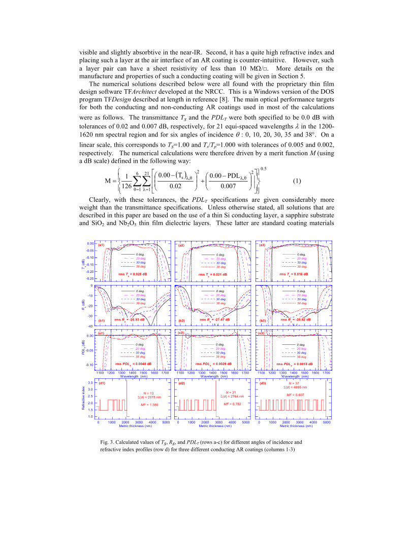
manufacture and properties of such a conducting coating will be given in Section 5. The numerical solutions described below were all found with the proprietary thin film
design software TFArchitect developed at the NRCC. This is a Windows version of the DOS
program TFDesign described at length in reference [8]. The main optical performance targets
for both the conducting and non-conducting AR coatings used in most of the calculations
were as follows. The transmittance Ts and the PDLT were both specified to be 0.0 dB with
tolerances of 0.02 and 0.007 dB, respectively, for 21 equi-spaced wavelengths λ in the 1200-
1620 nm spectral region and for six angles of incidence θ : 0, 10, 20, 30, 35 and 38°. On a
linear scale, this corresponds to Ts=1.00 and Ts/Tp=1.000 with tolerances of 0.005 and 0.002,
respectively. The numerical calculations were therefore driven by a merit function M (using
a dB scale) defined in the following way:
( )0.5
6
1θ
21
1λ
2
θλ,
2
θλ,s
0.007
PDL0.00
0.02
T0.00
126
1M
−+
−= ∑∑
= =
(1)
Clearly, with these tolerances, the PDLT specifications are given considerably more
weight than the transmittance specifications. Unless otherwise stated, all solutions that are
described in this paper are based on the use of a thin Si conducting layer, a sapphire substrate
and SiO2 and Nb2O5 thin film dielectric layers. These latter are standard coating materials
0 deg.
20 deg.
30 deg.
38 deg.
(a3)
rms Ts = 0.016 dB
-40
-30
-20
-10
0
0 deg.
20 deg.
30 deg.
38 deg.
Rs (dB)
(b1) rms Rs = -26.93 dB
0 deg.
20 deg.
30 deg.
38 deg.
(b2) rms Rs = -27.47 dB
0 deg.
20 deg.
30 deg.
38 deg.
(b3) rms Rs = -28.62 dB
-0.10
-0.05
0.00
0 deg.
20 deg.
30 deg.
38 deg.
1100 1200 1300 1400 1500 1600 1700
PDLT (dB
)
(c1)
Wavelength (nm)
rms PDLT = 0.0048 dB
0 deg.
20 deg.
30 deg.
38 deg.
(a2)
rms Ts = 0.021 dB
0 deg.
20 deg.
30 deg.
38 deg.
1100 1200 1300 1400 1500 1600 1700
(c2)
Wavelength (nm)
rms PDLT = 0.0029 dB
0 deg.
20 deg.
30 deg.
38 deg.
1100 1200 1300 1400 1500 1600 1700
(c3)
Wavelength (nm)
rms PDLT = 0.0018 dB
1.0
1.5
2.0
2.5
3.0
3.5
0 1000 2000 3000 4000 5000
Refractive index
N = 13
Σ(d) = 2078 nm
MF = 1.080
Metric thickness (nm)
(d1)
0 1000 2000 3000 4000 5000
N = 21
Σ(d) = 2764 nm
MF = 0.782
Metric thickness (nm)
(d2)
0 1000 2000 3000 4000 5000
N = 37
Σ(d) = 4895 nm
MF = 0.607
Metric thickness (nm)
(d3)
-0.25
-0.20
-0.15
-0.10
-0.05
0.00
0 deg.
20 deg.
30 deg.
38 deg.
Ts (dB
)
(a1)
rms Ts = 0.028 dB
Fig. 3. Calculated values of Ts, Rs, and PDLT (rows a-c) for different angles of incidence and
refractive index profiles (row d) for three different conducting AR coatings (columns 1-3)

that can be deposited by different methods including e-gun evaporation, ion plating, ion beam
plating, as well as RF- and AC magnetron sputtering. Both SiO2 and Nb2O5 layers are very
stable and mechanically robust.
The refractive index profiles and calculated performances of three different conducting
AR coatings designed on this basis are depicted in Fig. 3. The diagrams in columns 1, 2 and
3 correspond to solutions with progressively increasing overall total thickness and number of
layers. The spectral transmittances Ts of the three systems are shown in row (a). For clarity,
the data is plotted only for angles of incidence of 0, 20, 30 and 38°. Since conducting
coatings have a non-zero absorptance, T+R≠1.0, it was deemed desirable also to present the
calculated reflectance Rs in row (b). Similar information for the PDLT is provided in row (c).
The calculated rms values of Ts, Rs and PDLT (expressed in dB) for all the combinations of
wavelengths and angles of incidence which contributed to the merit function (Eq. (1)) are also
given in the diagrams of rows (a), (b), and (c). In all the above diagrams the spectral region
over which the performance is optimized is indicated by two vertical dotted lines. Finally, the
refractive index profiles, the number of layers, the total metric thicknesses and the calculated
merit functions MF of the systems are shown in the diagrams of row (d). The metric
thicknesses of the individual layers of the three solutions, together with the other numerical
data presented in Fig. 3, are also listed in Table 1.
Despite the use of a layer with a high refractive index at the AR/air interface, the
calculated performances of the AR coatings are quite impressive. As expected, with an
increasing number of layers and overall thickness, the performance of the AR coatings is
improved. The calculated performance of the system of Fig. 3 (c3) meets the specifications.
0 deg.
20 deg.
30 deg.
38 deg.
(a3)
rms Ts = 0.004 dB
-40
-30
-20
-10
00 deg.
20 deg.
30 deg.
38 deg.
Rs (dB
)
(b1)
rms Rs = -28.61 dB
0 deg.
20 deg.
30 deg.
38 deg.
(b2)
rms Rs = -34.37 dB
0 deg.
20 deg.
30 deg.
38 deg.
(b3)
rms Rs = -35.03 dB
-0.10
-0.05
0.00
0 deg.
20 deg.
30 deg.
38 deg.
1100 1200 1300 1400 1500 1600 1700
PDLT (dB)
(c1)
Wavelength (nm)
rms PDLT = 0.0022 dB
0 deg.
20 deg.
30 deg.
38 deg.
(a2)
rms Ts = 0.005 dB
0 deg.
20 deg.
30 deg.
38 deg.
1100 1200 1300 1400 1500 1600 1700
(c2)
Wavelength (nm)
rms PDLT = 0.0005 dB
0 deg.
20 deg.
30 deg.
38 deg.
1100 1200 1300 1400 1500 1600 1700
(c3)
Wavelength (nm)
rms PDLT = 0.0004 dB
1.0
1.5
2.0
2.5
3.0
3.5
0 1000 2000 3000 4000 5000
Refractive index
N = 10
Σ(d) = 1817 nm
MF = 0.362
Metric thickness (nm)
(d1)
0 1000 2000 3000 4000 5000
N = 19 Σ(d) = 2934 nm
MF = 0.182
Metric thickness (nm)
(d2)
0 1000 2000 3000 4000 5000
N = 33
Σ(d) = 5181 nm
MF = 0.160
Metric thickness (nm)
(d3)
-0.25
-0.20
-0.15
-0.10
-0.05
0.00
0 deg.
20 deg.
30 deg.
38 deg.
Ts (dB
)
(a1)
rms Ts = 0.008 dB
Fig. 4. Calculated values of Ts, Rs, and PDLT (rows a-c) for different angles of incidence and
refractive index profiles (row d) for three different non-conducting AR coatings (columns 1-3)

Table 1. Construction parameters and some properties of the layer systems
Fig.3, col.1 Fig.3, col.2 Fig.3, col.3 Fig.4, col.3 Fig.4, col.2 Fig.4, col.1 Fig.6, col.1 Fig.6, col.2
No. N d (nm) n d (nm) n d (nm) n d (nm) n d (nm) n d (nm) n d (nm) n d (nm)
subs. 1.747 1.747 1.747 1.747 1.747 1.747 1.747 1.747
1 1.462 64.94 1.462 75.16 1.462 92.22 1.462 90.18 1.462 119.77 1.462 56.65 1.397 57.06 1.462 99.38
2 2.227 42.59 2.227 35.51 2.227 27.89 2.227 18.41 2.227 20.22 2.227 33.46 2.227 42.16 2.227 28.99
3 1.462 577.94 1.462 292.78 1.462 358.64 1.462 465.82 1.462 348.91 1.462 562.99 1.397 583.24 1.462 340.36
4 2.227 376.10 2.227 38.24 2.227 48.47 2.227 44.20 2.227 62.83 2.227 328.12 2.227 350.43 2.227 46.14
5 1.462 54.65 1.462 167.93 1.462 124.08 1.462 159.14 1.462 125.82 1.462 247.99 1.397 70.33 1.462 139.18
6 2.227 242.99 2.227 109.20 2.227 130.95 2.227 45.40 2.227 78.23 2.227 50.01 2.227 317.70 2.227 135.64
7 1.462 126.89 1.462 201.85 1.462 209.40 1.462 428.15 1.462 406.08 1.462 111.23 1.397 144.88 1.462 168.74
8 2.227 51.66 2.227 27.25 2.227 48.11 2.227 49.50 2.227 62.50 2.227 173.01 2.227 49.33 2.227 56.20
9 1.462 201.27 1.462 253.27 1.462 195.85 1.462 166.63 1.462 77.85 1.462 252.66 1.397 158.44 1.462 248.78
10 2.227 162.35 2.227 184.86 2.227 142.54 2.227 59.26 2.227 128.65 2.227 0.70 2.227 156.37 2.227 107.68
11 1.462 165.03 1.462 91.75 1.462 196.35 1.462 317.71 1.462 352.44 1.397 165.64 1.462 191.25
12 3.656 10.00 2.227 34.14 2.227 59.14 2.227 73.24 2.227 47.39 3.656 10.00 2.227 55.12
13 1.462 2.00 1.462 323.93 1.462 182.33 1.462 148.99 1.462 69.28 1.462 2.00 1.462 237.91
14 2.227 198.14 2.227 138.59 2.227 67.61 2.227 179.54 2.227 140.04
15 1.462 106.39 1.462 235.23 1.462 391.40 1.462 273.92 1.462 155.01
16 2.227 41.05 2.227 64.37 2.227 65.67 2.227 31.45 2.227 47.67
17 1.462 255.02 1.462 141.15 1.462 163.99 1.462 123.58 1.462 285.21
18 2.227 153.38 2.227 133.96 2.227 107.41 2.227 179.77 2.227 137.88
19 1.462 162.54 1.462 258.36 1.462 153.05 1.462 245.91 1.462 147.12
20 3.656 10.00 2.227 40.24 2.227 132.86 2.227 42.90
21 1.462 2.00 1.462 59.59 1.462 178.93 1.462 274.83
22 2.227 71.31 2.227 89.34 2.227 183.90
23 1.462 70.38 1.462 162.67 1.462 92.96
24 2.227 103.49 2.227 109.69 2.227 34.45
25 1.462 244.04 1.462 291.79 1.462 325.93
26 2.227 191.33 2.227 56.89 2.227 221.56
27 1.462 42.49 1.462 111.75 1.462 110.14
28 2.227 77.86 2.227 175.40 2.227 27.30
29 1.462 283.28 1.462 250.97 1.462 289.93
30 2.227 213.63 2.227 38.18 2.227 153.90
31 1.462 82.63 1.462 139.19 1.462 167.97
32 2.227 46.62 2.227 175.64 3.656 10.00
33 1.462 253.98 1.462 251.68 1.462 2.00
34 2.227 151.76
35 1.462 162.28
36 3.656 10.00
37 1.462 2.00
air 1.000 1.000 1.000 1.000 1.000 1.000 1.000 1.000
Σd 2078.41 2764.39 4894.57 5180.75 2934.12 1816.81 2107.59 4706.04
MF 1.080 0.782 0.607 0.160 0.182 0.362 0.894 1.630
RMS Ts 0.0275 0.0206 0.0164 0.0044 0.0050 0.0081 0.0223 0.0452
RMS Rs -26.93 -27.470 -28.616 -35.031 -34.368 -28.605 -27.704 -26.077
RMS PDL 0.0048 0.0029 0.0018 0.0004 0.0005 0.0022 0.0042 0.0037

3. Non-conducting AR coating designs for 0<θθθθ<38º
As stated above, only one of the AR coatings on the sapphire window needs to be conducting.
The overall performance of the window would be improved if the second AR coating were to
be made entirely out of dielectric materials. In Fig. 4 are shown the calculated performances
and refractive index profiles of three such systems. For easier comparison, the data in this
diagram is presented in the same way as in Fig. 3. These results were derived from the
systems of Fig. 3, by removing the capping SiO2 layer and by replacing the Si layer by a
Nb2O5 layer. Each system was then refined. It will be seen that in the refinement process the
thicknesses of the layers were considerably modified, the total number of layers was changed,
and that, in two cases, the thin high refractive index Nb2O5 layers at the air interface were
removed (see Table 1). Not surprisingly in each instance the transmittance losses were
reduced over those for the corresponding conducting coatings. It will also be seen from this
diagram that there is little gain in performance by increasing the number of layers of the
system from 19 to 33.
Figure 5 illustrates the significance of using different AR coatings on the two sides of four
otherwise identical sapphire windows. Columns 1 and 2 show the calculated Ts and PDLT
values for one and for four-coated windows. The graphs in row (a) correspond to substrates
in which identical conducting AR coatings of the 37-layer design depicted in graph c3 of Fig.
3 are applied to all surfaces. In this figure all the Ts and PDLT values shown correspond to an
angle of incidence of 38º. In the graphs in row (b), all AR coatings correspond to the 19-layer
non-conducting design of graph c2 of Fig. 4. This of course is not an option since one of the
AR coatings on each window must be conducting, but the results are presented here for
comparison purposes. The graphs in row (c) assume that one side of each window is coated
with the design of graph c3 of Fig. 3, and the other side with the design of graph c2 of Fig. 4.
Clearly, for best results, conducting and non-conducting AR coatings should be combined -
this is the preferred option.
Fig. 5. Calculated Ts, PDLT values (columns 1, 2) for 38º incidence of four windows placed in series, each
with two AR-coated surfaces: row a – two conducting ARs of Fig. 3 d3; row b – two non-conducting ARs of Fig. 4 d2; row c – one conducting and one non-conducting AR.

4. Other conducting AR coating designs
In this Section we present two additional examples to illustrate the fact that conducting AR
coatings with a similar performance can also be designed for other specifications and that
solutions can be found that are based on other coating materials.
All the AR coatings described thus far have essentially been based on the use of SiO2 and
Nb2O5 layers. Of course, other materials could also have been used. The specifications for
the example depicted in column 1 of Fig. 6 are exactly the same as those for the systems
depicted in Fig. 3. However, this time the design is based on ZnS and MgF2, materials that
can be readily evaporated from resistance-heated sources or by electron beam guns. Such a
process might lend itself to larger area coatings, provided that it can be sufficiently well
controlled. The conducting Si layer and its native oxide layer are the same as in the other
designs. It will be seen from this figure that the calculated performance of this system is, if
anything, somewhat better than that of the Nb2O5/SiO2 system of comparable thickness and
number of layers. This is due to the fact that the refractive index of MgF2 is lower than that
of SiO2.
The next design was based on the same AR specifications as before except now the angle
of incidence range was extended to 55º. In column 2 of Fig. 6 are shown the calculated
results for a conducting AR coating made of the same materials that were used in the design
of the systems depicted in Fig. 3. Not surprisingly, it can be seen from Fig. 6 that although
Fig. 6 Calculated values of Ts, Rs, PDLT (rows a-c) for different angles of incidence θ and
refractive index profiles (row d) for two additional conducting AR coatings: column 1–AR coating
based on ZnS and MgF2 coating materials; column 2 –AR coating designed for angles of incidence
0< θ <55º.

the calculated results for the solution found are still quite good, extending the angle of
incidence range has somewhat compromised the performance.
5. Manufacture and experimental results
Before proceeding to the manufacture of a multilayer it is always prudent to carry out an error
analysis to see if the system is sensitive to errors in the layer thicknesses or refractive indices.
Reasonable thickness errors correspond to 1% of a layer’s thickness for thicker layers and up
to a maximum of 1 nm for thinner layers. For this reason we have carried out, for each of the
systems depicted in Fig. 3, two sets of 50 calculations on systems in which the individual
layers were randomly perturbed with thickness errors not exceeding 1% and 1 nm,
respectively. The calculations were performed at an angle of incidence of 38º, the most
critical case. In Fig. 7, rows (a)-(c) correspond to the results for the three different systems
and in columns 1 and 2 are plotted the upper and lower envelopes for Ts and PDLT curves
within which one would expect the performance of 66% of the AR coatings manufactured
with the above type of thickness error to fall. From these curves one can conclude that the
chances of successfully manufacturing these coatings are good. An analysis of the effect of
random errors in the thin film refractive indices was not performed because layer-to-layer
reproducibility of the optical constants is very good for the deposition process proposed for
the manufacture of the coatings.
A similar set of calculations on the 19-layer system of Fig. 4 (d2) shows that the
sensitivity to thickness errors of the non-conducting AR coatings is smaller than that of the
conducting AR coatings. This is not surprising as a 1 nm thickness error in the Si layer in the
conducting coatings represents a 10% change in the thickness of that layer which, in turn, has
a significant effect on the absorption of the system. This problem does not exist in the non-
conducting AR coatings.
The 37-layer system shown in Fig. 3, column 3 was selected to be manufactured as it
provides a very good conducting AR performance. This coating was deposited on an AC
magnetron sputtering system similar to the one described in reference [9]. The same system
was also used for the manufacture of the Iridian entry to the Manufacturing Problem at the
2001 Topical Meeting on Optical Interference Coatings in Banff [10]. The interested reader is
Fig. 7. Sensitivity of the calculated values of Ts, and PDLT for 38º incidence of the conducting AR coatings of Fig. 3 (rows a-c) to 1% and 1 nm random errors (columns 1, 2) in the layer thicknesses
(see text for details)

referred to these two papers for more detail on the deposition system and process control used
for manufacturing the prototype conducting AR coating. Here we will only state that in-situ
measurements were made to determine layer thicknesses accurately while real-time re-
optimization was used to minimize the effects of small thickness errors that occurred during
the deposition of the individual layers.
The deposition of the (amorphous) Si layer posed some unique challenges. It is important
to purge the deposition chamber of any oxygen during deposition to avoid the Si layer
oxidizing during deposition but it is also necessary to expose the Si layer to atomic oxygen
after deposition in order to stabilize and protect the Si layer. Therefore, after depositing the
oxide layers, the oxygen flow was stopped and the Si targets were pre-sputtered in an argon
only plasma until the oxide layer was removed from the Si targets. The Si layer was then
deposited after which oxygen was re-introduced into the chamber and the Si layer was
oxidized forming a ~2 nm protective oxide layer. Note that the Si layer was deposited with a
thickness that took into account the amount of material that would be oxidized during the
formation of the protective oxide layer. More information on the protection of thin metal
layers from oxidation will be found in Ref. [11].
For the prototype conducting AR-coated window, the same conducting AR coating was
deposited on both sides of a c-axis sapphire crystal. A monitor slide of BK7 was used in the
AR coating runs for the in-situ measurements. Figure 8 shows that there is good agreement
between the transmission measurements of the completed AR systems taken in-situ on the
monitoring slides and the calculated transmittances based on the determination of the
individual layers during the deposition. Further, the results are almost exactly the same for
the AR coatings on both sides. The deposition process is therefore very predictable and
repeatable. The transmittance measurements were made on a Perkin-Elmer UV/VIS/NIR
Lambda 19 spectrophotometer.
Figure 9 shows the transmittance of a bare sapphire substrate and the prototype
conducting AR coated sapphire window at normal incidence along with the theoretical
desired and calculated transmittance curves. As can be seen there is good agreement between
the desired and the calculated transmittance curves, where the calculated curve is based on the
layer thicknesses determined during the deposition run. The difference between the measured
and desired theoretical curves is within 1.2% which implies that for a single conducting AR
coating, the difference between desired and measured is around 0.6%.
To look at the Si layer absorption, Fig. 10 shows the near-normal transmittance and
reflectance of the prototype conducting AR coated window along with their sum. Within the
measurement accuracy there appears to be no significant amount of absorption in the layer
system in the spectral range of interest.
Fig. 8. Monitoring precision for an experi-
mental conducting AR coating of the type depicted in column 3 of Fig. 3. Figures a
and b compare the calculated and the
measured in-situ transmittances of moni-toring slides for the AR coatings deposited
on sides A and B
Fig. 9. Comparison of the measured normal
incidence transmittances of a substrate with the target transmittance and the transmittance
calculated from the thicknesses of the layers
determined during the deposition. In this and subsequent diagrams, the two sides of each
substrate carry the same conducting AR coating.
0.80
0.85
0.90
0.95
1.00
calculated
measured
Tra
nsm
itta
nce (a)
monitor slide A
0.80
0.85
0.90
0.95
1.00
calculated
measured
1100 1200 1300 1400 1500 1600 1700
Tra
nsm
itta
nce (b)
W avelength (nm)
monitor slide B0.86
0.88
0.90
0.92
0.94
0.96
0.98
1.00
desired curve
calculated curve
measured curve
bare sapphire
1100 1200 1300 1400 1500 1600 1700
Tra
nsm
itta
nce
W avelength (nm)
0o, air-to-air

The transmittance of the prototype conducting AR coated window was measured using a
swept laser system for an angle of incidence of 40° over the 1540 to 1620 nm wavelength
region for un-polarized and p-polarized light (Fig. 11). Within this wavelength region, the
measured and calculated transmittance curves are within 1% of each other and, as well, the p-
polarized and un-polarized data are in good agreement with each other indicating that the
PDL of these coatings is low.
To test the conductivity of the AR coating it is necessary to make an ohmic contact with
the 10 nm thick amorphous Si layer. Attempts to measure conductivity with a conventional
four-point probe were unsuccessful, apparently because the probe tips would fracture the Si
layer. Proper measurement of conductivity requires evaporation of suitably thick (100 – 200
nm thick) and separate metal onto the Si layer, preferably immediately after the Si layer is
deposited and before the protective oxide layer is formed. We expect that this coating will be
at least somewhat sensitive to environmental effects, as exposure of the early samples to
water slightly decreased the transmission. The best procedure for forming ohmic contact to
the conducting layer, and the effects of environmental exposure to the thin Si layer, will be
the subject of a follow-on study. It is worth noting that the intended application of this
window for hermetic and antistatic sealing of MEMS devices (as shown in Figure 1) requires
a conductive layer only in the controlled environment of the interior of the hermetically-
sealed package. The outer layer required low reflectivity and PDL, but does not incorporate
the conducting Si layer.
6. Conclusions
It has been shown in this paper that, using conventional coating materials, it is possible to
design AR coatings that are effective both over a fairly broad spectral region (λlong/λshort ≈
1.40) and a wide range of angles of incidence (0-38º, or even 0-55º). Not only is the
theoretical transmittance of windows treated with such coatings quite high, but they also have
very good polarization independence (low PDLT values).
The coatings can incorporate a thin amorphous Si upper layer which should provide a
conductive surface of approximately 10MΩ/ sheet resistivity. Despite the high refractive
index of this layer, is was possible to generate designs without significant impact on the
transmittance over the 1200-1630 nm design wavelength, such that low optical loss
components using multiple passes through the window become practical. When windows
with conducting AR coatings are attached to a metallic housing, they can protect the contents
from electrostatic fields and prevent the attraction of dust particles. This should be of interest
in the construction of MEMS. If the conducting AR systems are made predominantly of
oxide layers, it should be possible to make robust brazed connections to the metallic housing.
The range of coating materials can be expanded if a lower temperature bonding process, such
as conducting cement, is used.
0.80
0.85
0.90
0.95
1.00
T
T+R
Tra
nsm
itta
nce, re
flecta
nce, (T+R
) (a)
0.00
0.05
0.10
0.15
0.20
R
1100 1200 1300 1400 1500 1600 1700Wavelength (nm)
0.94
0.95
0.96
0.97
0.98
0.99
1.00
calculated 40o
measured 40o
1100 1200 1300 1400 1500 1600 1700
Tra
nsm
itta
nce
Wavelength (nm)
40o, air-to-air
Fig. 10 Measured normal incidence
transmittance T, reflectance R and the sum (T+R).
Fig. 11 Comparison of the calculated and
measured transmittance for unpolarized and p-polarized light incident at 40˚ of an
AR coating prepared during run 3.

As in most optical thin film problems, the performance of the AR coatings depends on the
overall optical thickness and the number of layers in the system. In this paper, examples were
given of coatings consisting of up to 37 layers. If a better performance was required and if
economic considerations were to permit it, this number could readily be expanded to more
than 60 layers. All the AR coatings discussed in this paper were designed for sapphire
substrates but there are no reasons why similar coatings could not be produced for other
window materials such as Si, fused quartz and various specialty glasses. Further, it should be
possible to design similar coatings for other spectral regions although the Si layer might have
to be replaced by a different conducting material that has a small extinction coefficient at the
chosen wavelengths. One of the designs, depicted in Fig. 3 (d3), was produced experimentally and its measured
optical performance was in reasonable agreement with the calculated curves for both
unpolarized and p-polarized light. With further work, it should be possible to achieve an even
better agreement between the desired and measured performance. It was not possible to
measure the sheet resistance of the sample using conventional four-point probe methods. A
procedure for forming ohmic contact to the conducting layer, and the effects of environmental
exposure to the thin Si layer, will be the subject of another paper.
Acknowledgments
The authors would like to thank Dr. Penghui Ma for suggesting that thin Si layers might have
a suitable sheet resistance and that the native oxide on their surface would protect them from
further oxidation.