computer architectur by fm sir
TRANSCRIPT

8/7/2019 Computer Architectur by FM Sir
http://slidepdf.com/reader/full/computer-architectur-by-fm-sir 1/23
Internal connection between processor & memory:
Fig: Internal Connection between Processor & Memory.
MAR:
MAR means Memory Address Register.
It holds the address of the main memory from where data is to be transferred.
PC: PC means Program Counter.
It holds the address of the next instructions.
IR:
IR means Instruction Register.
It stores the instruction that is currently being executed.
It gives the operation to the CU to generate the timing signal that controls the
execution.
MDR:
MDR means Memory Data Register / Buffer Register.
It holds the data which write into / Read out of address location.
Register:
General purpose register R 0 through R n+1 is used for storing data.
CU:
CU means Control Unit.
The memory, arithmetic & logic, input & output units store & process
information & perform input / output operation. These operation units must be
co-ordinate in same way. This is the task of the CU.

8/7/2019 Computer Architectur by FM Sir
http://slidepdf.com/reader/full/computer-architectur-by-fm-sir 2/23
Send control signal to other units and sense their state.
ALU:
ALU means Arithmetic Logic Unit.
It perform the arithmetic operation like addition, subtraction etc.
Bus:
It is a common path way connecting two or more devices.
It is a shared transmission medium.
At a time only one device should be transmitted signal.
Width of Bus:
Width of Bus means at a time how many amount of data (bit) can be transferred.
Single Bus Structure:
The system structure where all units are connected to a bus.
The bus can be used for only one transfer at a time so that only two units can
actively use the bus at any given time.
Fig: Single Bus Structure
Advantages:
Low cost
Flexibility
Easy to design
Disadvantages:
Only one data transfer at a time. Time consuming to any program.
MultipleBus Structure:
The system structure where multiple buses are used.
Multiple buses active more concurrently in operation by allowing two or more
transfers.

8/7/2019 Computer Architectur by FM Sir
http://slidepdf.com/reader/full/computer-architectur-by-fm-sir 3/23
Fig: Multiple Bus structure
Advantages:
Allows the system to support a wider rarity of devices.
More speed than single bus structure.
Disadvantage:
Low performance due to the more devices greater the bus length propagation
delays.
The bus become bottleneck as the aggregate data transfer rate increase
towards the capacity of the bus.
High Speed Architecture:
High speed bus brings high devices closer to the Processor.
High speed buses are used.
They are independent to the processor.

8/7/2019 Computer Architectur by FM Sir
http://slidepdf.com/reader/full/computer-architectur-by-fm-sir 4/23
Fig: High Speed Architecture
Advantage:
High speed
Disadvantage:
Costly
Implementation is very difficult
System Bus:
A bus that connect major components (Processor, memory, I/O).
It consists of 50 to 100 separate lines; each line is used for a particular purpose.
50 to 100 lines can classify into functional groups.
i. Data lines.
ii. Address lines.
iii. Control lines.
Fig: System Bus
i. Data bus:
It transmits or transfer data between various modules.
Data lines are collectively called data bus.
ii. Address bus:
Address lines are collectively called address bus.

8/7/2019 Computer Architectur by FM Sir
http://slidepdf.com/reader/full/computer-architectur-by-fm-sir 5/23
4-bit address bus means 24
= 16 B. So, if address width is 20 bit
then 220
= 1 MB.
iii. Control bus:
Control lines are collectively called control bus.
Used to control signals.
Bus Arbitration:
The process of selecting bus master. That means select the device which can transmit
data on the bus right now.
Only one bus master at a time.
Several devices may complete for the control of the bus but one gets the control.
Daisy Chaining Approach:
Every device must be set a priority.
If device1 priority is greater than other device then device1 is selected as a bus master.
Fig: Daisy Chaining Approach
Advantage:
Very simple concept
Centralized, very easy to select bus master.
Synchronizing process.
Disadvantage:
Starvation problem (bored for waiting)
Propagation delay
The entire system fails if the higher priority device fails.
Distributed Arbitration:
Distributed Arbitration means that all devices waiting to use the bus that have equal
responsibility in carrying out the arbitration process, without using a central arbiter.
Each device on the bus is assigned a 4-bit identification number.
When one or more devices request the bus, they assert the ���� �������� signal
and place their 4-bit ID numbers on their open collector lines, through .

8/7/2019 Computer Architectur by FM Sir
http://slidepdf.com/reader/full/computer-architectur-by-fm-sir 6/23
Fig: Distributed Arbitration
Advantages:
Higher reliability due to the operation of the bus is not dependent on any single
device.
PCI Bus:
PCI means Peripheral Component Interaction.
It has high bandwidth & it is very popular.
It is an independent bus that can function as a peripheral bus.
It requires very few chips to implement & supports other busses connected to
it.
It used centralized arbitration scheme.
It can be used in both signal Processor (desktop system) & multiprocessor
(server system) system.

8/7/2019 Computer Architectur by FM Sir
http://slidepdf.com/reader/full/computer-architectur-by-fm-sir 7/23
Fig: PCI Bus in Desktop System.
Fig: PCI Bus in Server System.
PnP:
PnP means Plug and Play.
The device which we insert into the computer & it automatically recognized &
configured in computer is called PnP.
Intel created the PnP standard and incorporated it into the design for PCI.

8/7/2019 Computer Architectur by FM Sir
http://slidepdf.com/reader/full/computer-architectur-by-fm-sir 8/23
Q.
h¡
t thin¢
s are required to i£
plement a PnP?
¤ olution:
To fully impleme ¥
¦
PnP re § uires three things ̈
PnP Bios:
The core utility that enables PnP and detects PnP devices©
Extended
ystem Confi
uration Data (ESCD): A file that contains information about installed PnP devices
PnP operatin
system: Any operating system, such as Windows 95/98/ME/XP/Win7, that
supports PnP. PnP handlers in the operating system complete the
configuration process started by the B OS for each PnP device.
Q. hat are the key tasks for PnP automates?
Solution:
PnP automates several key tasks that were typically done either manually or with an
installation utility provided by the hardware manufacturer. These tasks include the setting of: Interrupt Request (IRQ):
H/W interrupts to get the automation of CPU.
Direct memory access (DMA): The device is configured to access the system memory without
consulting the CPU first.
Memory addresses: Many devices are assigned a section of system memory for exclusive
use by that device. This ensures that the hardware will have the needed
resources to operate properly.
Input / Output (I/O) confi
uration: This setting defines the ports used by the device for receiving and
sending information.
Q. hat will be happen if a new PCI based sound card is added to a PC?
Solution:
If a new PCI based sound card is added to a PC, then it performs some tasks. Those
tasks are given below:
The system BIOS initiates the PnP BIOS.
The PnP BIOS scans the PCI bus for hardware by sending out a signal to any device connected to the bus & asking the device who it is.
The sound card responds by identif ying itself. The device ID is sent back across
the bus to the BIOS.
The PnP BIOS checks the ESCD to search the configuration data for the sound
card. Since the sound card was just installed, there is no existing ESCD record
for it.
The PnP BIOS assigns IRQ , DMA, memory address and I/O settings to the sound
card and saves the data in the ESCD.
8/7/2019 Computer Architectur by FM Sir
http://slidepdf.com/reader/full/computer-architectur-by-fm-sir 9/23
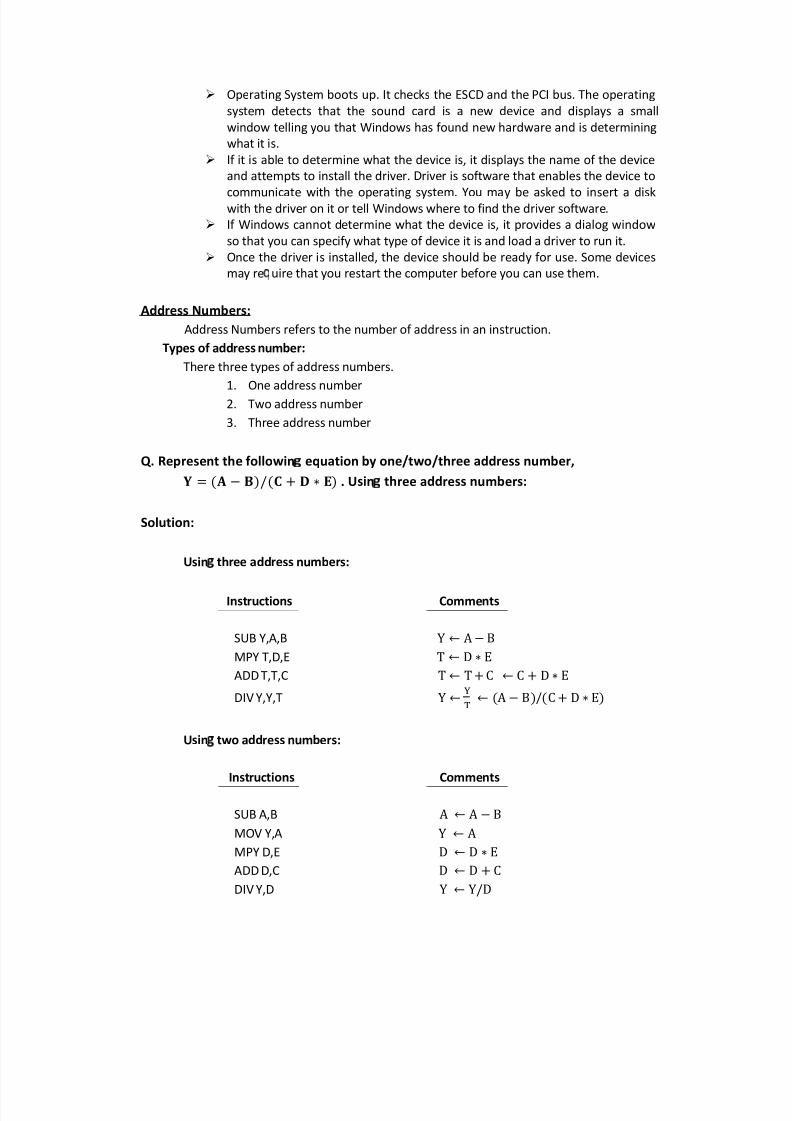
Operating System boots up. It checks the ESCD and the PCI bus. The operating
system detects that the sound card is a new device and displays a small
window telling you that Windows has found new hardware and is determining
what it is.
If it is able to determine what the device is, it displays the name of the device
and attempts to install the driver. Driver is software that enables the device to
communicate with the operating system. You may be asked to insert a diskwith the driver on it or tell Windows where to find the driver software.
If Windows cannot determine what the device is, it provides a dialog window
so that you can specif y what type of device it is and load a driver to run it.
Once the driver is installed, the device should be ready for use. Some devices
may re
uire that you restart the computer before you can use them.
Address Numbers:
Address Numbers ref ers to the number of address in an instruction.
Types of address number:
There three types of address numbers.
1. One address number
2. Two address number
3. Three address number
Q. Represent the followin
equation by one/two/three address number,
. Usin
three address numbers:
Solution:
Usin
three address numbers:
Instructions Comments
SUB Y,A,B
MPY T,D,E
ADDT,T,C
DIVY,Y,T
Usin!
two address numbers:
Instructions Comments
SUB A,B
MOV Y,A
MPY D,E
ADD D,C
DIVY,D

8/7/2019 Computer Architectur by FM Sir
http://slidepdf.com/reader/full/computer-architectur-by-fm-sir 10/23
Usin"
one address number: [by usin"
Accumulator (AC)]
Instructions Comments
LOAD E
MPY D
ADDC
STORE Y
LOAD A
SUB B
DIVY
STORE Y
Usin#
one address number: [by without usin#
Accumulator (AC)]
Instructions
LOAD A
SUB B
STORE A
LOAD E
MPYD
ADDC
STORE C
LOAD A
DIV C
STORE Y
Pipelinin$
:
It is a process in which several storages of the CPU are used to execute more than one
instruction concurrently.
It is an eff ective way of organizing concurrently activity in any system.
A pipelined processor may process each instruction in four steps:
Fetch : Read the instruction from the memory.
Decode : Decode the instruction & f etch the source operand.
Execute : Perform the operation specified by instruction.
Write : Store the result in the destination location.
Example:
W
E
D
F

8/7/2019 Computer Architectur by FM Sir
http://slidepdf.com/reader/full/computer-architectur-by-fm-sir 11/23
Fig: Pipelining
Normally for instruction needs clock cycle. But with the
use of pipeline it is done with 7 clock cycle.
Super Pipelining:
Its an alternative approach to achieve better performance.
Many pipeline stages perform task that requires less than half of a clock cycle, so a
double interval clock speed allow the performance of two tasks in one clock cycle.
Example:
Fig: Super Pipelining
Supper Scalar:
A Super Scalar process consists of multiple independent pipelines.
Each pipeline consists of multiple stages, so that each one can handle multiple
instructions at a time.

8/7/2019 Computer Architectur by FM Sir
http://slidepdf.com/reader/full/computer-architectur-by-fm-sir 12/23
Example:
Fig: Supper Scalar
Q . Consider that, four instructions to execute and each has 4 steps (F, D,
E, W%
. Each part/steps take 2 clock cycles to execute. Compare the performance of (i)
Pipelining (ii) Super pipelining & (iii) Scalar pipelining.
Solution:
Using Pipelining:
Fig: Pipelining
Using Super Pipelining

8/7/2019 Computer Architectur by FM Sir
http://slidepdf.com/reader/full/computer-architectur-by-fm-sir 13/23
Fig: Super Pipelining
Using Scalar Pipelining
Fig: Scalar Pipelining
In the above discussion, we see that, Pipelining needs 14 clock cycles, super
pipelining needs 11 clock cycles but Super Scalar needs only 10 clock cycles.
Problems of super scalar:
Data dependency:
In this case, of instruction depend on the results of . Procedure dependency:
Resource conflict:
Instruction Level Parallelism:
The degree to which the instruction of a program can be executed parallels is called
instruction level parallelism.

8/7/2019 Computer Architectur by FM Sir
http://slidepdf.com/reader/full/computer-architectur-by-fm-sir 14/23
Fig: 4
thdegree
Effect of branch on pipelining:
Branch Condition:
A conditional branch instruction introduces the added caused by the dependency of
the branch condition on the result of a preceding instruction.
Branch Penalty:
F & D steps block the buffer until solve of the branch condition, in this situation we
need some time to free this buffer. This time is called branch penalty.
Fig: Branch Penalty.

8/7/2019 Computer Architectur by FM Sir
http://slidepdf.com/reader/full/computer-architectur-by-fm-sir 15/23
Logic to deal with branch:
Fig: Logic to deal with branch.
Different ways of implementing a multiprocessor:
Multiprocessor System:
A machine that includes an efficient high bandwidth medium for communication
among the multiple processors, memory devices of I/O devices.
There are three ways to implement a multiprocessor system:
(i) Uniform Memory Access (UMA).
(ii)
Non-uniform memory Access (NUMA).(iii) Distributed Memory Access (DMA).
Uniform Memory Access (UMA):
An interconnection network permits processors to access memories so that
any of the processors can access any of the memories.
The interconnection network introduces considerable delay for each memory
access.
If this delay is same for all memory access then it is an UMA system.

8/7/2019 Computer Architectur by FM Sir
http://slidepdf.com/reader/full/computer-architectur-by-fm-sir 16/23
Fig: Uniform Memory Access
Non-uniform memory Access (NUMA):
Memory modules are attached directly to the processor. Each processor can access its own memories (local) as well as the other processors
memories via network.
If local memory access time is and other memory access time isthen
.In this case, it is called Non-uniform memory access.
Fig: Non-uniform memory Access
Distributed Memory Access (DMA):
All memory modules are private to their corresponding processor.
A processor can not access a remote memory without the cooperation of the
remote processor. Ex. Processor cant access the memory of until permit.
Permission procedure is implementing by message exchanged via the network.

8/7/2019 Computer Architectur by FM Sir
http://slidepdf.com/reader/full/computer-architectur-by-fm-sir 17/23
Fig: Distributed Memory Access
Q . What is RISC & CISC?
Solution:
RISC
: RISC means Reduced instruction Set Computer.
It has large number of general purpose register (32).
Limited & simple instruction set (24).
Optimized instruction pipelining.
Example:
LOAD B, [address]
MPY A, B
STORE [address], AAdvantage:
For pipelining it has fast execution rate.
Uses VLSI technology.
Disadvantages:
Needed more instruction than CISC to perform the same task. So, it is less effective
than CISC.
CISC:
CISC means Complex Instruction Set Computer.
Small number of general purpose registers (8).
Complex and huge number of instruction set (215).
Example:
MPY [adress1], [address2]

8/7/2019 Computer Architectur by FM Sir
http://slidepdf.com/reader/full/computer-architectur-by-fm-sir 18/23
Advantage:
Program size or length smaller.
Consume less memory for storing a program.
Low page fault due to smaller program.
Disadvantage:
Instructions are so complex, so, cant optimize easily.
Cost is higher than RISC.
Q . What are SISD, SIMD, MISD, and MIMD?
Solution:
SISD:
SISD means Single Instruction Single Data.
A single processor can execute a single instruction stream to operate on data
stored in a single memory.
Central unit send single instruction to processing unit then processing unit execute
and store this data to memory unit.
Example: Uniprocessor.
SIMD:
SIMD means Single Instruction Multiple Data.
A single instruction stream is executed by multiple processing elements.
Each processing element has an associate memory so that each instruction is
executed on a different set of data by the processors.

8/7/2019 Computer Architectur by FM Sir
http://slidepdf.com/reader/full/computer-architectur-by-fm-sir 19/23
Example: Vector Processor, Array Processor.
MISD:
MISD means Multiple Instruction Single Data.
A sequence of instructions stream are executed by a number of processors by
using data from a single memory.
Example: Systolic Array.
MIMD:
MIMD means Multiple Instruction Multiple Data.
A set of processors simultaneously execute different instruction stream by using
different data sets.
There are two types, such as Shared memory system & Distributed memory
system.

8/7/2019 Computer Architectur by FM Sir
http://slidepdf.com/reader/full/computer-architectur-by-fm-sir 20/23
Fig: Shared Memory Schema. Fig: Distributed Memory System.
Q . Describe about ROM, PROM, EPROM, EEPROM & Flash memory.
Solution:
ROM:
ROM means Read Only Memory.
It is an IC programmed with data when manufactured.
It is used not only computer but also in electrical devices like toys.
It contains grid of columns and rows where the columns & rows intersect.
A ROM chip needs programming of perfect and complicated data during
manufactured.
There is a cell. If we send a current with high voltage above then forward break
over, the appropriate column with the selective row will selected.
If any error is found then the chip thrown away & again we need manufactured.
Advantages:
Low power consumption.
Cost effective.
Extremely reliable.
Disadvantages:
It is one time device.
If any error then it is not usable.

8/7/2019 Computer Architectur by FM Sir
http://slidepdf.com/reader/full/computer-architectur-by-fm-sir 21/23
PROM:
PROM means Programmable Read Only Memory.
Creating ROM chip is time consuming & expensive. So, we need to think another
device like PROM.
PROM inexpensive & can be programmed with a tool called programmer.
Like ROM it has grids of columns & rows but the difference is in every intersection
between rows and columns there is a fuse.
Fuse is connected to logical 1 [+5V to +10V]. So, at the initial state, all cells contain
logical 1. To change the value of a cell 1 to 0 the programmer is used to set a
specific amount current to the cell. The higher voltage breaks the connection
between rows and columns by burning out the fuse that means burning out the
PROM.
If we want bring logical 1 to 0 then apply fixed amount of current then it goes 1 to
0 and fuse is burn.
Advantage:
After manufacture can be programmed but only once.
Disadvantage:
PROM is expensive than other device.
It cant program more than one.
EPROM:
EPROM means Erasable Programmable Read Only Memory.
It can be overwritten many times.
It special type memory device that retrain its content until the ultraviolet (UV) light
is exposed, the UV light clear it contents making it possible to reprogram thememory.
To write and erase an EPROM you need a tool called EPROM programmer.
Each cell contain two transmitter separated by an oxide layer. One of them is
known as floating point gate & another is known as control gate.
The floating point gate is connected to the row via the control gate.There is a link
between them. As long as link is in place the cell contains 1.

8/7/2019 Computer Architectur by FM Sir
http://slidepdf.com/reader/full/computer-architectur-by-fm-sir 22/23
To change 1 to 0 re&
uire a process called Flower Northeim Tunneling. It changes
the position of electron in the floating gate.
An electron charge (10V to 30V) is applied to the floating gate. This change causes
the floating point gate act as electron gun. Its the barrier between floating point
gate & control gate.
Advantages:
Easy to program.
Rewritten many times.
Disadvantages:
To erase data from EPROM needs UV light.
EEPROM:
EEPROM means Electrically Erasable Programmable Read Only Memory'
.
The entire chip does not have to completely erase to change a specific portion. Changing the content does not need additional re
( uirement instead of UV light,
the electron are return to the normal position by applying electric field to each
cell. This erases the target cell of the EEPROM.
EEPORM sort by hybrid between a static RAM and EPROM So that data can be
changed easily.
Advantages:
A single portion can be updated, need not change whole portion.
Disadvantage:
At a time more than one byte cant be changed.
Its much slower.
After 10000 to 40000 writes the chip will be completely dead.
Flash Memory:
A flash cell is based on a single transistor controlled by trapped charge, just like an
EEPROM cell.
There are some diff erences between flash and EEPROM. In EEPROM it is possible
to read and write the contents of a single cell. In a flash device it is possible to read
the contents of a single cell, but it is only possible to write an entire block of cells.Prior to writing, the previous contents of the block are erased.
Advantages:
Flash devices have greater density, which leads to higher capacity and a lower
cost per bit.
They re)
uire a single power supply voltage and consume less power in their
operation.

8/7/2019 Computer Architectur by FM Sir
http://slidepdf.com/reader/full/computer-architectur-by-fm-sir 23/23
Q.0
hat are the diff erences between RAM & ROM?
Solution:
The diff erences between RAM & ROM are given below:
Both RAM & ROM provide the user random access to stored data.
RAM provide only short term memory since data stored in RAM is lost when power
is turned off, but ROM provide long term storage since data is permanently store
here.
RAMs data fre1
uently & speedy be altered & changed, but ROM can not be
reconfigured.