computer-aided design concept to silicon victor p. nelson
Post on 19-Dec-2015
217 views
TRANSCRIPT

Computer-Aided Computer-Aided DesignDesign
Concept to SiliconConcept to Silicon
Victor P. NelsonVictor P. Nelson

ASIC Design FlowASIC Design FlowBehavioral
ModelVHDL/Verilog
Gate-LevelNetlist
Transistor-LevelNetlist
PhysicalLayout
Map/Place/Route
DFT/BIST& ATPG
VerifyFunction
VerifyFunction
Verify Function& Timing
Verify Timing
DRC & LVSVerification
IC Mask Data/FPGA Configuration File
Standard Cell IC & FPGA/CPLD
Synthesis
Test vectors Full-custom IC

Mentor Graphics CAD Tools Mentor Graphics CAD Tools (select from “eda” list in user-setup on the Sun (select from “eda” list in user-setup on the Sun
network)network) ICFlow2007.2ICFlow2007.2– For custom & standard cell IC designs– For custom & standard cell IC designs
– IC flow toolsIC flow tools (Design Architect-IC, IC Station, Calibre)(Design Architect-IC, IC Station, Calibre)– Digital/analog/mixed simulation Digital/analog/mixed simulation (Modelsim,ADVance (Modelsim,ADVance
MS,Eldo,MachTA)MS,Eldo,MachTA)– HDL SynthesisHDL Synthesis (Leonardo)(Leonardo)
DFT/2006.3DFT/2006.3– ATPG/DFT/BIST toolsATPG/DFT/BIST tools (DFT Advisor, Flextest, Fastscan) (DFT Advisor, Flextest, Fastscan)
Modelsim/6.3c Modelsim/6.3c (HDL Simulation)(HDL Simulation) FPGA/2004FPGA/2004 (FPGA Advantage, Modelsim, Leonardo)(FPGA Advantage, Modelsim, Leonardo) *Xilinx/ISE8.2i *Xilinx/ISE8.2i (Xilinx FPGA/CPLD - back end design)(Xilinx FPGA/CPLD - back end design) *QuartusII/5.0*QuartusII/5.0 (Altera FPGA/CPLD - back end design)(Altera FPGA/CPLD - back end design) *Ims/6.2*Ims/6.2 (IMS chip tester)(IMS chip tester)
* Vendor-Provided (Not Mentor Graphics) Tools* Vendor-Provided (Not Mentor Graphics) Tools

Mentor Graphics ASIC Design Kit Mentor Graphics ASIC Design Kit (ADK)(ADK)
Technology files & standard cell librariesTechnology files & standard cell libraries– AMI: ami12, ami05 AMI: ami12, ami05 (1.2, 0.5 (1.2, 0.5 μμm)m)– TSMC: tsmc035, tsmc025, tsmc018 TSMC: tsmc035, tsmc025, tsmc018 (0.35, 0.25, 0.18 (0.35, 0.25, 0.18 μμm)m)
IC flow & DFT tool support files:IC flow & DFT tool support files:– Simulation Simulation
VHDL/Verilog/Mixed-Signal modelsVHDL/Verilog/Mixed-Signal models (Modelsim/ADVance MS)(Modelsim/ADVance MS) Analog (SPICE) modelsAnalog (SPICE) models (Eldo/Accusim)(Eldo/Accusim) Post-layout timing Post-layout timing (Mach TA)(Mach TA) Digital schematic Digital schematic ((Quicksim II, Quicksim Pro)Quicksim II, Quicksim Pro) (exc. (exc.
tsmc025,tsmc018)tsmc025,tsmc018)– Synthesis to std. cells Synthesis to std. cells (LeonardoSpectrum)(LeonardoSpectrum)– Design for test & ATPG Design for test & ATPG (DFT Advisor, Flextest/Fastscan)(DFT Advisor, Flextest/Fastscan)– Schematic capture Schematic capture (Design Architect-IC)(Design Architect-IC)– IC physical design (standard cell & custom) IC physical design (standard cell & custom)
Floorplan, place & route Floorplan, place & route (IC Station)(IC Station) Design rule check, layout vs schematic, parameter extraction Design rule check, layout vs schematic, parameter extraction
(Calibre)(Calibre)

Xilinx/Altera FPGA/CPLD DesignXilinx/Altera FPGA/CPLD Design Simulate designs in Simulate designs in ModelsimModelsim
– Behavioral models (VHDL,Verilog)Behavioral models (VHDL,Verilog)– Synthesized netlists (VHDL, Verilog)Synthesized netlists (VHDL, Verilog)
Requires “primitives” library for the target technologyRequires “primitives” library for the target technology Synthesize netlist from behavioral modelSynthesize netlist from behavioral model
– LeonardoLeonardo has libraries for most FPGAs has libraries for most FPGAs– Xilinx ISEXilinx ISE has its own synthesis tool has its own synthesis tool
Vendor tools for back-end design Vendor tools for back-end design – Map, place, route, configure device, timing analysis, generate Map, place, route, configure device, timing analysis, generate
timing modelstiming models– Xilinx Xilinx Integrated Software EnvironmentIntegrated Software Environment (ISE) (ISE)– Altera Altera Quartus II & Max+Plus2Quartus II & Max+Plus2
Higher level tools for system design & managementHigher level tools for system design & management– Mentor Graphics Mentor Graphics FPGA AdvantageFPGA Advantage– Xilinx Platform Studio : Xilinx Platform Studio : SoC design, IP management, HW/SW SoC design, IP management, HW/SW
codesigncodesign

Behavioral Design & Behavioral Design & VerificationVerification
(mostly technology-independent)(mostly technology-independent)
Create Behavioral/RTL HDL Model(s)
Simulate to VerifyFunctionality
SynthesizeCircuit
LeonardoSpectrum,Xilinx ISE(digital)
ModelSim (digital)
VHDL-AMSVerilog-A
ADVance MS (analog/mixed signal)
VHDLVerilog
SystemC
Technology LibrariesPost-Layout Simulation,
Technology-Specific Netlistto Back-End Tools

ADVance MS Simulation ADVance MS Simulation SystemSystem
ADVance MS “kernel” supports:ADVance MS “kernel” supports:– VHDL & Verilog: digital VHDL & Verilog: digital (via ModelSim)(via ModelSim)– VHDL-AMS & Verilog-A: analog/mixed VHDL-AMS & Verilog-A: analog/mixed
signalsignal– Eldo/SPICE: analog Eldo/SPICE: analog (via Eldo)(via Eldo)– Eldo RF/SPICE: analog RF Eldo RF/SPICE: analog RF (via Eldo RF)(via Eldo RF)– Mach TA/SPICE: high-speed analog/timingMach TA/SPICE: high-speed analog/timing
Invoke stand-alone or from Design Invoke stand-alone or from Design Architect-ICArchitect-IC

ADVance MSADVance MSDigital, Analog, Mixed-Signal Digital, Analog, Mixed-Signal
SimulationSimulation
ADVance MS
WorkingLibrary
Design_1Design_2
VITAL
IEEE 1164 ResourceLibraries
SimulationSetup
EZwaveor Xelga
InputStimuli
VHDL,Verilog,VHDL-AMS, Verilog-A,
SPICE Netlists
Eldo,Eldo RF ModelSim
View ResultsMach TAMach PA
Analog(SPICE) Digital
(VHDL,Verilog)
Mixed Signal(VHDL-AMS, Verilog-A)
SPICEmodels
Xilinxsimprims

Example: 4-bit binary Example: 4-bit binary countercounter
VHDL modelVHDL model (count4.vhd)(count4.vhd)
– Create working library: Create working library: vlib workvlib work vmap work workvmap work work– Compile: Compile: vcom count4.vhdvcom count4.vhd– Simulate: Simulate: vsim count4(rtl)vsim count4(rtl)
ModelSim simulation-control inputsModelSim simulation-control inputs– ModelSimModelSim “Macro” “Macro” (count4_rtl.do)(count4_rtl.do)
– OR, VHDL testbenchOR, VHDL testbench ModelSim resultsModelSim results
– listinglisting or or waveformwaveform

-- count4.vhd 4-bit parallel-load synchronous counter-- count4.vhd 4-bit parallel-load synchronous counterLIBRARY ieee;LIBRARY ieee;USE ieee.std_logic_1164.all; USE ieee.numeric_std.all; USE ieee.std_logic_1164.all; USE ieee.numeric_std.all; --synthesis libraries--synthesis libraries
ENTITY count4 ISENTITY count4 IS PORT (clock,clear,enable,load_count : IN STD_LOGIC;PORT (clock,clear,enable,load_count : IN STD_LOGIC;
D: IN unsigned(3 downto 0);D: IN unsigned(3 downto 0); Q: OUT unsigned(3 downto 0));Q: OUT unsigned(3 downto 0));END count4;END count4;
ARCHITECTURE rtl OF count4 ISARCHITECTURE rtl OF count4 ISSIGNAL int : unsigned(3 downto 0);SIGNAL int : unsigned(3 downto 0);BEGINBEGIN PROCESS(clear, clock, enable)PROCESS(clear, clock, enable) BEGIN BEGIN IF (clear = '1') THEN IF (clear = '1') THEN int <= "0000";int <= "0000"; ELSIF (clock'EVENT AND clock='1') THEN ELSIF (clock'EVENT AND clock='1') THEN IF (enable = '1') THEN IF (enable = '1') THEN
IF (load_count = '1') THENIF (load_count = '1') THEN int <= D;int <= D; ELSEELSE
int <= int + "01";int <= int + "01"; END IF;END IF; END IF;END IF; END IF;END IF; END PROCESS; END PROCESS; Q <= int;Q <= int;END rtl;END rtl;

Test stimulus:Test stimulus:Modelsim “do” file: Modelsim “do” file:
count4_rtl.docount4_rtl.doadd wave /clock /clear /enable /load_count /D /Qadd wave /clock /clear /enable /load_count /D /Qadd list /clock /clear /enable /load_count /D /Qadd list /clock /clear /enable /load_count /D /Qforce /clock 0 0, 1 10 -repeat 20force /clock 0 0, 1 10 -repeat 20force /clear 0 0, 1 5, 0 10force /clear 0 0, 1 5, 0 10force /enable 0 0, 1 25force /enable 0 0, 1 25force /load_count 0 0, 1 20, 0 35, 1 330, 0 350force /load_count 0 0, 1 20, 0 35, 1 330, 0 350force /D 10#5 0, 10#9 300force /D 10#5 0, 10#9 300run 400run 400

Testbench: Testbench: count4_bench.vhdcount4_bench.vhdLIBRARY ieee; USE ieee.std_logic_1164.all; USE ieee.numeric_std.all;LIBRARY ieee; USE ieee.std_logic_1164.all; USE ieee.numeric_std.all;
ENTITY count4_bench is end count4_bench;ENTITY count4_bench is end count4_bench;ARCHITECTURE test of count4_bench isARCHITECTURE test of count4_bench is component count4component count4 PORT (clock,clear,enable,load_count : IN STD_LOGIC;PORT (clock,clear,enable,load_count : IN STD_LOGIC;
D: IN unsigned(3 downto 0);D: IN unsigned(3 downto 0); Q: OUT unsigned(3 downto 0));Q: OUT unsigned(3 downto 0)); end component;end component; for all: count4 use entity work.count4(behavior);for all: count4 use entity work.count4(behavior); signal clk : STD_LOGIC := '0';signal clk : STD_LOGIC := '0'; signal clr, en, ld: STD_LOGIC;signal clr, en, ld: STD_LOGIC; signal din, qout: unsigned(3 downto 0);signal din, qout: unsigned(3 downto 0);beginbegin UUT: count4 port map(clk,clr,en,ld,din,qout);UUT: count4 port map(clk,clr,en,ld,din,qout); clk <= not clk after 10 ns;clk <= not clk after 10 ns; P1: processP1: process beginbegin din <= "0101"; clr <= '1'; en <= '1'; ld <= '1';din <= "0101"; clr <= '1'; en <= '1'; ld <= '1'; wait for 10 ns;wait for 10 ns; clr <= '0'; clr <= '0'; wait for 20 ns;wait for 20 ns; ld <= '0';ld <= '0'; wait for 200 ns;wait for 200 ns; end process;end process;end;end;
Alternative to “do” file
Could also check results &“assert” error messages

Count4 – Simulation Count4 – Simulation waveformwaveform
ParallelLoad
Counting
Clear

ADVance MS : mixed-signal ADVance MS : mixed-signal simulationsimulation
A/D converter
digital
analogVHDL-AMS

ADVance MS: mixed Verilog-SPICEADVance MS: mixed Verilog-SPICE
SPICEsubcircuit
Verilog top(test bench)

Automated Synthesis with Automated Synthesis with Leonardo SpectrumLeonardo Spectrum
Leonardo Spectrum(Level 3)
VHDL/Verilog Behavioral/RTL Models
FPGA
ASIC
TechnologySynthesis Libraries
Technology-SpecificNetlist
DesignConstraints
VHDL, Verilog, SDF,EDIF, XNF
Level 1 – FPGALevel 2 – FPGA + TimingLevel 3 – ASIC + FPGA
ADKAMI 0.5, 1.2TSMC 0.35, 0.25

Leonardo – ASIC Synthesis Leonardo – ASIC Synthesis FlowFlow

Leonardo synthesis procedureLeonardo synthesis procedure
1.1. Invoke Invoke leonardoleonardo2.2. Select & load a technology library Select & load a technology library (ASIC or (ASIC or
FPGA)FPGA)– ASIC > ADK > TSMC 0.35 micronASIC > ADK > TSMC 0.35 micron
3.3. Read input VHDL/Verilog file(s): Read input VHDL/Verilog file(s): count4.vhdcount4.vhd
4.4. Enter any constraints (clock freq, delays, etc.)Enter any constraints (clock freq, delays, etc.)5.5. Optimize for area/delay/effort levelOptimize for area/delay/effort level6.6. Write output file(s)Write output file(s)
– count4_0.vhdcount4_0.vhd - VHDL netlist - VHDL netlist– count4.vcount4.v - Verilog netlist - Verilog netlist (for IC layout)(for IC layout)– count4.sdf count4.sdf - Standard delay format file - Standard delay format file (for (for
timing)timing)– count4.edf count4.edf - EDIF netlist - EDIF netlist (for Xilinx/Altera FPGA)(for Xilinx/Altera FPGA)

Leonardo-synthesized netlist count4_0.vhdLeonardo-synthesized netlist count4_0.vhdlibrary IEEE; use IEEE.STD_LOGIC_1164.all;library IEEE; use IEEE.STD_LOGIC_1164.all;library adk; use adk.adk_components.all; -- ADDED BY VPNlibrary adk; use adk.adk_components.all; -- ADDED BY VPNentity count4 isentity count4 is port (port ( clock : IN std_logic ; clear : IN std_logic ; enable : IN std_logic ; load_count : IN std_logic ;clock : IN std_logic ; clear : IN std_logic ; enable : IN std_logic ; load_count : IN std_logic ; D : IN std_logic_vector (3 DOWNTO 0) ; Q : OUT std_logic_vector (3 DOWNTO 0)) ;D : IN std_logic_vector (3 DOWNTO 0) ; Q : OUT std_logic_vector (3 DOWNTO 0)) ;end count4 ;end count4 ;
architecturearchitecture netlist netlist of count4 isof count4 is -- rtl changed to netlist by VPN -- rtl changed to netlist by VPN signal Q_3_EXMPLR, Q_2_EXMPLR, Q_1_EXMPLR, Q_0_EXMPLR, nx8, nx14, nx22, signal Q_3_EXMPLR, Q_2_EXMPLR, Q_1_EXMPLR, Q_0_EXMPLR, nx8, nx14, nx22, nx28, nx48, nx54, nx62, nx126, nx136, nx146, nx156, nx169, nx181, nx28, nx48, nx54, nx62, nx126, nx136, nx146, nx156, nx169, nx181, nx183, nx185, nx187, nx189: std_logic ;nx183, nx185, nx187, nx189: std_logic ;beginbegin Q(3) <= Q_3_EXMPLR ; Q(2) <= Q_2_EXMPLR ; Q(1) <= Q_1_EXMPLR ; Q(0) <= Q_0_EXMPLR ;Q(3) <= Q_3_EXMPLR ; Q(2) <= Q_2_EXMPLR ; Q(1) <= Q_1_EXMPLR ; Q(0) <= Q_0_EXMPLR ; Q_0_EXMPLR_EXMPLR : dffr port map ( Q=>Q_0_EXMPLR, QB=>OPEN, D=>nx126, CLK=>clock, R=>clear);Q_0_EXMPLR_EXMPLR : dffr port map ( Q=>Q_0_EXMPLR, QB=>OPEN, D=>nx126, CLK=>clock, R=>clear); ix127 : mux21_ni port map ( Y=>nx126, A0=>Q_0_EXMPLR, A1=>nx8, S0=>enable );ix127 : mux21_ni port map ( Y=>nx126, A0=>Q_0_EXMPLR, A1=>nx8, S0=>enable ); ix9 : oai21 port map ( Y=>nx8, A0=>load_count, A1=>Q_0_EXMPLR, B0=>nx169 );ix9 : oai21 port map ( Y=>nx8, A0=>load_count, A1=>Q_0_EXMPLR, B0=>nx169 ); ix170 : nand02 port map ( Y=>nx169, A0=>D(0), A1=>load_count);ix170 : nand02 port map ( Y=>nx169, A0=>D(0), A1=>load_count); Q_1_EXMPLR_EXMPLR : dffr port map ( Q=>Q_1_EXMPLR, QB=>OPEN, D=>nx136, CLK=>clock, Q_1_EXMPLR_EXMPLR : dffr port map ( Q=>Q_1_EXMPLR, QB=>OPEN, D=>nx136, CLK=>clock,
R=>clear);R=>clear); ix137 : mux21_ni port map ( Y=>nx136, A0=>Q_1_EXMPLR, A1=>nx28, S0=> enable);ix137 : mux21_ni port map ( Y=>nx136, A0=>Q_1_EXMPLR, A1=>nx28, S0=> enable); ix29 : ao22 port map ( Y=>nx28, A0=>D(1), A1=>load_count, B0=>nx14, B1=> nx22);ix29 : ao22 port map ( Y=>nx28, A0=>D(1), A1=>load_count, B0=>nx14, B1=> nx22); ix15 : or02 port map ( Y=>nx14, A0=>Q_0_EXMPLR, A1=>Q_1_EXMPLR);ix15 : or02 port map ( Y=>nx14, A0=>Q_0_EXMPLR, A1=>Q_1_EXMPLR); ix23 : aoi21 port map ( Y=>nx22, A0=>Q_1_EXMPLR, A1=>Q_0_EXMPLR, B0=> load_count);ix23 : aoi21 port map ( Y=>nx22, A0=>Q_1_EXMPLR, A1=>Q_0_EXMPLR, B0=> load_count); Q_2_EXMPLR_EXMPLR : dffr port map ( Q=>Q_2_EXMPLR, QB=>OPEN, D=>nx146, CLK=>clock, R=>clear);Q_2_EXMPLR_EXMPLR : dffr port map ( Q=>Q_2_EXMPLR, QB=>OPEN, D=>nx146, CLK=>clock, R=>clear); ix147 : mux21_ni port map ( Y=>nx146, A0=>Q_2_EXMPLR, A1=>nx48, S0=> enable);ix147 : mux21_ni port map ( Y=>nx146, A0=>Q_2_EXMPLR, A1=>nx48, S0=> enable); ix49 : oai21 port map ( Y=>nx48, A0=>nx181, A1=>nx183, B0=>nx189);ix49 : oai21 port map ( Y=>nx48, A0=>nx181, A1=>nx183, B0=>nx189); ix182 : aoi21 port map ( Y=>nx181, A0=>Q_1_EXMPLR, A1=>Q_0_EXMPLR, B0=> Q_2_EXMPLR);ix182 : aoi21 port map ( Y=>nx181, A0=>Q_1_EXMPLR, A1=>Q_0_EXMPLR, B0=> Q_2_EXMPLR); ix184 : nand02 port map ( Y=>nx183, A0=>nx185, A1=>nx187);ix184 : nand02 port map ( Y=>nx183, A0=>nx185, A1=>nx187); ix186 : inv01 port map ( Y=>nx185, A=>load_count);ix186 : inv01 port map ( Y=>nx185, A=>load_count); ix188 : nand03 port map ( Y=>nx187, A0=>Q_2_EXMPLR, A1=>Q_1_EXMPLR, A2=> Q_0_EXMPLR);ix188 : nand03 port map ( Y=>nx187, A0=>Q_2_EXMPLR, A1=>Q_1_EXMPLR, A2=> Q_0_EXMPLR); ix190 : nand02 port map ( Y=>nx189, A0=>D(2), A1=>load_count);ix190 : nand02 port map ( Y=>nx189, A0=>D(2), A1=>load_count); Q_3_EXMPLR_EXMPLR : dffr port map ( Q=>Q_3_EXMPLR, QB=>OPEN, D=>nx156, CLK=>clock, R=>clear);Q_3_EXMPLR_EXMPLR : dffr port map ( Q=>Q_3_EXMPLR, QB=>OPEN, D=>nx156, CLK=>clock, R=>clear); ix157 : mux21_ni port map ( Y=>nx156, A0=>Q_3_EXMPLR, A1=>nx62, S0=> enable);ix157 : mux21_ni port map ( Y=>nx156, A0=>Q_3_EXMPLR, A1=>nx62, S0=> enable); ix63 : mux21_ni port map ( Y=>nx62, A0=>nx54, A1=>D(3), S0=>load_count);ix63 : mux21_ni port map ( Y=>nx62, A0=>nx54, A1=>D(3), S0=>load_count); ix55 : xnor2 port map ( Y=>nx54, A0=>Q_3_EXMPLR, A1=>nx187);ix55 : xnor2 port map ( Y=>nx54, A0=>Q_3_EXMPLR, A1=>nx187);end netlist ;end netlist ;

// Verilog description for cell count4, LeonardoSpectrum Level 3, // Verilog description for cell count4, LeonardoSpectrum Level 3, 2005a.82 2005a.82
module count4 ( clock, clear, enable, load_count, D, Q ) ;module count4 ( clock, clear, enable, load_count, D, Q ) ; input clock ;input clock ; input clear ;input clear ; input enable ;input enable ; input load_count ;input load_count ; input [3:0]D ;input [3:0]D ; output [3:0]Q ;output [3:0]Q ;
wire nx8, nx14, nx22, nx28, nx48, nx54, nx62, nx126, nx136, nx146, nx156, nx169, nx181, nx183, wire nx8, nx14, nx22, nx28, nx48, nx54, nx62, nx126, nx136, nx146, nx156, nx169, nx181, nx183, nx185, nx187, nx189;nx185, nx187, nx189;
wire [3:0] \$dummy ;wire [3:0] \$dummy ;
dffr Q_0__rename_rename (.Q (Q[0]), .QB (\$dummy [0]), .D (nx126), .CLK (clock), .R (clear)) ;dffr Q_0__rename_rename (.Q (Q[0]), .QB (\$dummy [0]), .D (nx126), .CLK (clock), .R (clear)) ; mux21_ni ix127 (.Y (nx126), .A0 (Q[0]), .A1 (nx8), .S0 (enable)) ;mux21_ni ix127 (.Y (nx126), .A0 (Q[0]), .A1 (nx8), .S0 (enable)) ; oai21 ix9 (.Y (nx8), .A0 (load_count), .A1 (Q[0]), .B0 (nx169)) ;oai21 ix9 (.Y (nx8), .A0 (load_count), .A1 (Q[0]), .B0 (nx169)) ; nand02 ix170 (.Y (nx169), .A0 (D[0]), .A1 (load_count)) ;nand02 ix170 (.Y (nx169), .A0 (D[0]), .A1 (load_count)) ; dffr Q_1__rename_rename (.Q (Q[1]), .QB (\$dummy [1]), .D (nx136), .CLK (clock), .R (clear)) ;dffr Q_1__rename_rename (.Q (Q[1]), .QB (\$dummy [1]), .D (nx136), .CLK (clock), .R (clear)) ; mux21_ni ix137 (.Y (nx136), .A0 (Q[1]), .A1 (nx28), .S0 (enable)) ;mux21_ni ix137 (.Y (nx136), .A0 (Q[1]), .A1 (nx28), .S0 (enable)) ; ao22 ix29 (.Y (nx28), .A0 (D[1]), .A1 (load_count), .B0 (nx14), .B1 (nx22) ) ;ao22 ix29 (.Y (nx28), .A0 (D[1]), .A1 (load_count), .B0 (nx14), .B1 (nx22) ) ; or02 ix15 (.Y (nx14), .A0 (Q[0]), .A1 (Q[1])) ;or02 ix15 (.Y (nx14), .A0 (Q[0]), .A1 (Q[1])) ; aoi21 ix23 (.Y (nx22), .A0 (Q[1]), .A1 (Q[0]), .B0 (load_count)) ;aoi21 ix23 (.Y (nx22), .A0 (Q[1]), .A1 (Q[0]), .B0 (load_count)) ; dffr Q_2__rename_rename (.Q (Q[2]), .QB (\$dummy [2]), .D (nx146), .CLK (clock), .R (clear)) ;dffr Q_2__rename_rename (.Q (Q[2]), .QB (\$dummy [2]), .D (nx146), .CLK (clock), .R (clear)) ; mux21_ni ix147 (.Y (nx146), .A0 (Q[2]), .A1 (nx48), .S0 (enable)) ;mux21_ni ix147 (.Y (nx146), .A0 (Q[2]), .A1 (nx48), .S0 (enable)) ; oai21 ix49 (.Y (nx48), .A0 (nx181), .A1 (nx183), .B0 (nx189)) ;oai21 ix49 (.Y (nx48), .A0 (nx181), .A1 (nx183), .B0 (nx189)) ; aoi21 ix182 (.Y (nx181), .A0 (Q[1]), .A1 (Q[0]), .B0 (Q[2])) ;aoi21 ix182 (.Y (nx181), .A0 (Q[1]), .A1 (Q[0]), .B0 (Q[2])) ; nand02 ix184 (.Y (nx183), .A0 (nx185), .A1 (nx187)) ;nand02 ix184 (.Y (nx183), .A0 (nx185), .A1 (nx187)) ; inv01 ix186 (.Y (nx185), .A (load_count)) ;inv01 ix186 (.Y (nx185), .A (load_count)) ; nand03 ix188 (.Y (nx187), .A0 (Q[2]), .A1 (Q[1]), .A2 (Q[0])) ;nand03 ix188 (.Y (nx187), .A0 (Q[2]), .A1 (Q[1]), .A2 (Q[0])) ; nand02 ix190 (.Y (nx189), .A0 (D[2]), .A1 (load_count)) ;nand02 ix190 (.Y (nx189), .A0 (D[2]), .A1 (load_count)) ; dffr Q_3__rename_rename (.Q (Q[3]), .QB (\$dummy [3]), .D (nx156), .CLK (clock), .R (clear)) ;dffr Q_3__rename_rename (.Q (Q[3]), .QB (\$dummy [3]), .D (nx156), .CLK (clock), .R (clear)) ; mux21_ni ix157 (.Y (nx156), .A0 (Q[3]), .A1 (nx62), .S0 (enable)) ;mux21_ni ix157 (.Y (nx156), .A0 (Q[3]), .A1 (nx62), .S0 (enable)) ; mux21_ni ix63 (.Y (nx62), .A0 (nx54), .A1 (D[3]), .S0 (load_count)) ;mux21_ni ix63 (.Y (nx62), .A0 (nx54), .A1 (D[3]), .S0 (load_count)) ; xnor2 ix55 (.Y (nx54), .A0 (Q[3]), .A1 (nx187)) ;xnor2 ix55 (.Y (nx54), .A0 (Q[3]), .A1 (nx187)) ;endmoduleendmodule

Post-synthesis simulationPost-synthesis simulation((LeonardoLeonardo-generated netlist)-generated netlist)
Verify synthesized netlist matches Verify synthesized netlist matches behavioral modelbehavioral model
Create simulation primitives library for std Create simulation primitives library for std cells:cells:
>vlib adk>vlib adk>vcom $ADK/technology/adk.vhd>vcom $ADK/technology/adk.vhd>vcom $ADK/technology/adk_comp.vhd>vcom $ADK/technology/adk_comp.vhd
Insert library/package declaration into Insert library/package declaration into netlistnetlist
library adk;library adk;use adk.adk_components.all;use adk.adk_components.all;
Simulate in Modelsim, using “do file” or test bench Simulate in Modelsim, using “do file” or test bench from original behavioral simulation from original behavioral simulation – results should matchresults should match
VITALmodels of all ADK std cells

Leonardo can generate SDF (std. delay format) file Leonardo can generate SDF (std. delay format) file with technology-specific, VITAL-compliant timing with technology-specific, VITAL-compliant timing parameters.parameters.
(CELLTYPE "dffr")(CELLTYPE "dffr") (INSTANCE Q_0_EXMPLR_EXMPLR)(INSTANCE Q_0_EXMPLR_EXMPLR) (DELAY(DELAY (ABSOLUTE(ABSOLUTE (PORT D (::0.00) (::0.00))(PORT D (::0.00) (::0.00)) (PORT CLK (::0.00) (::0.00))(PORT CLK (::0.00) (::0.00)) (PORT R (::0.00) (::0.00))(PORT R (::0.00) (::0.00)) (IOPATH CLK Q (::0.40) (::0.47))(IOPATH CLK Q (::0.40) (::0.47)) (IOPATH R Q (::0.00) (::0.55))(IOPATH R Q (::0.00) (::0.55)) (IOPATH CLK QB (::0.45) (::0.36))(IOPATH CLK QB (::0.45) (::0.36)) (IOPATH R QB (::0.53) (::0.00))))(IOPATH R QB (::0.53) (::0.00)))) (TIMINGCHECK(TIMINGCHECK (SETUP D (posedge CLK) (0.47))(SETUP D (posedge CLK) (0.47)) (HOLD D (posedge CLK) (-0.06))))(HOLD D (posedge CLK) (-0.06))))
Post-synthesis timing Post-synthesis timing analysisanalysis
Path delays(min:typ:max)
Delays lumpedat pins
Constraints

VITAL Model (1)VITAL Model (1)library IEEE; use IEEE.STD_LOGIC_1164.all;library IEEE; use IEEE.STD_LOGIC_1164.all;use IEEE.VITAL_Primitives.all; use IEEE.VITAL_Timing.all;use IEEE.VITAL_Primitives.all; use IEEE.VITAL_Timing.all;entity and02 isentity and02 is generic (generic (
tipd_A0 : VitalDelayType01Z := VitalZeroDelay01Z;tipd_A0 : VitalDelayType01Z := VitalZeroDelay01Z;tipd_A1 : VitalDelayType01Z := VitalZeroDelay01Z;tipd_A1 : VitalDelayType01Z := VitalZeroDelay01Z;tpd_A0_Y : VitalDelayType01Z := VitalZeroDelay01Z;tpd_A0_Y : VitalDelayType01Z := VitalZeroDelay01Z;tpd_A1_Y : VitalDelayType01Z := VitalZeroDelay01Ztpd_A1_Y : VitalDelayType01Z := VitalZeroDelay01Z
););port (port (
A0 : in STD_LOGIC;A0 : in STD_LOGIC;A1 : in STD_LOGIC;A1 : in STD_LOGIC;Y : out STD_LOGICY : out STD_LOGIC
););attribute VITAL_LEVEL0 of and02 : entity is TRUE;attribute VITAL_LEVEL0 of and02 : entity is TRUE;
end and02;end and02;

VITAL Model (2)VITAL Model (2)architecture and02_arch of and02 isarchitecture and02_arch of and02 is
attribute VITAL_LEVEL1 of and02_arch : architecture is TRUE;attribute VITAL_LEVEL1 of and02_arch : architecture is TRUE;signal A0_ipd : STD_LOGIC := 'X';signal A0_ipd : STD_LOGIC := 'X';signal A1_ipd : STD_LOGIC := 'X';signal A1_ipd : STD_LOGIC := 'X';
beginbeginWireDelay : BlockWireDelay : Blockbeginbegin
VitalWireDelay (A0_ipd, A0, tipd_A0);VitalWireDelay (A0_ipd, A0, tipd_A0);VitalWireDelay (A1_ipd, A1, tipd_A1);VitalWireDelay (A1_ipd, A1, tipd_A1);
end Block;end Block;
VitalBehavior : Process (A0_ipd, A1_ipd)VitalBehavior : Process (A0_ipd, A1_ipd)VARIABLE INT_RES_0 : STD_LOGIC := 'X';VARIABLE INT_RES_0 : STD_LOGIC := 'X';VARIABLE GlitchData_Y : VitalGlitchDataType;VARIABLE GlitchData_Y : VitalGlitchDataType;
beginbegin-- FUNCTIONALITY SECTION ---- FUNCTIONALITY SECTION --INT_RES_0 := VitalAnd2 (A0_ipd, A1_ipd);INT_RES_0 := VitalAnd2 (A0_ipd, A1_ipd);

VITAL Model (3)VITAL Model (3)-- PATH DELAY SECTION ---- PATH DELAY SECTION --VitalPathDelay01Z (VitalPathDelay01Z (
OutSignal => Y,OutSignal => Y,OutSignalName => "Y",OutSignalName => "Y",OutTemp => INT_RES_0,OutTemp => INT_RES_0,Paths => (Paths => (
0 => ( 0 => ( InputChangeTime => InputChangeTime => A0_ipd'LAST_EVENT,A0_ipd'LAST_EVENT,
PathDelay => tpd_A0_Y,PathDelay => tpd_A0_Y,PathCondition => TRUEPathCondition => TRUE
),),1 => ( 1 => ( InputChangeTime => InputChangeTime =>
A1_ipd'LAST_EVENT,A1_ipd'LAST_EVENT,PathDelay => tpd_A1_Y,PathDelay => tpd_A1_Y,PathCondition => TRUEPathCondition => TRUE
))),),GlitchData => GlitchData_Y,GlitchData => GlitchData_Y,Mode => OnDetect,Mode => OnDetect,MsgOn => TRUE, Xon => TRUE,MsgOn => TRUE, Xon => TRUE,MsgSeverity => WARNINGMsgSeverity => WARNING

Design for test & test Design for test & test generationgeneration
Consider test during the Consider test during the designdesign phase phase– Test design more difficult after design frozenTest design more difficult after design frozen
Basic steps:Basic steps:– Design for test (DFT) – insert test points, scan Design for test (DFT) – insert test points, scan
chains, etc. to improve testabilitychains, etc. to improve testability– Insert built-in self-test (BIST) circuitsInsert built-in self-test (BIST) circuits– Generate test patterns (ATPG)Generate test patterns (ATPG)– Determine fault coverage (Fault Simulation)Determine fault coverage (Fault Simulation)

DFT & test design flowDFT & test design flow
Memory& LogicBIST Boundary
Scan
InternalScan Design
ATPG

DFTadvisor/FastScan Design DFTadvisor/FastScan Design FlowFlow
Source: FlexTest Manual
DFT/ATPGLibrary:adk.atpg
count4.vhd
count4_0.vhdcount4.v
count4_scan.v

ASIC DFT FlowASIC DFT Flow
Insert Internal Scan Circuitry
Generate/VerifyTest Vectors
Synthesized VHDL/Verilog Netlist
adk.atpg
ATPG Library
DFT Advisor
Fastscan/Flextest
VHDL/VerilogNetlist With
Scan Elements
Test Pattern File

Example DFTadvisor sessionExample DFTadvisor session Invoke: Invoke:
– dftadvisor –verilog count4.v –lib dftadvisor –verilog count4.v –lib $ADK/technology/adk.atpg$ADK/technology/adk.atpg
Implement scan with defaults:Implement scan with defaults: (full scan, mux-DFF scan elements)(full scan, mux-DFF scan elements)
– set system mode setupset system mode setup– analyze control signals –autoanalyze control signals –auto– set system mode dftset system mode dft– runrun– insert test logicinsert test logic– write netlist count4_scan.v –verilogwrite netlist count4_scan.v –verilog– write atpg setup count4_scan write atpg setup count4_scan (creates count4_scan.dofile for ATPG in Fastscan)(creates count4_scan.dofile for ATPG in Fastscan)

count4 – without scan designcount4 – without scan design

count4 – scan inserted by count4 – scan inserted by DFTadvisorDFTadvisor

ATPG with FastScan ATPG with FastScan (full-scan circuit)(full-scan circuit)
Invoke: Invoke: – fastscan –verilog count4.v –lib fastscan –verilog count4.v –lib
$ADK/technology/adk.atpg$ADK/technology/adk.atpg Generate test pattern file in FastScan:Generate test pattern file in FastScan:
– dofile count4_scan.dofile dofile count4_scan.dofile (defines scan path & (defines scan path & procedure)procedure)
– set system mode atpgset system mode atpg– create patterns –auto create patterns –auto (generate test patterns)(generate test patterns)– save patternssave patterns
Note: “count4_scan.dofile” created by DFTadvisor

Test file: scan chain definition Test file: scan chain definition and load/unload proceduresand load/unload procedures
scan_group "grp1" =scan_group "grp1" = scan_chain "chain1" =scan_chain "chain1" = scan_in = "/scan_in1";scan_in = "/scan_in1"; scan_out = "/output[3]";scan_out = "/output[3]"; length = 4;length = 4; end;end; procedure shift "grp1_load_shift" =procedure shift "grp1_load_shift" = force_sci "chain1" 0;force_sci "chain1" 0; force "/clock" 1 20;force "/clock" 1 20; force "/clock" 0 30;force "/clock" 0 30; period 40;period 40; end;end; procedure shift "grp1_unload_shift" procedure shift "grp1_unload_shift"
== measure_sco "chain1" 10;measure_sco "chain1" 10; force "/clock" 1 20;force "/clock" 1 20; force "/clock" 0 30;force "/clock" 0 30; period 40;period 40; end;end;
procedure load "grp1_load" =procedure load "grp1_load" = force "/clear" 0 0;force "/clear" 0 0; force "/clock" 0 0;force "/clock" 0 0; force "/scan_en" 1 0;force "/scan_en" 1 0; apply "grp1_load_shift" 4 40;apply "grp1_load_shift" 4 40; end;end;procedure unload "grp1_unload" =procedure unload "grp1_unload" = force "/clear" 0 0;force "/clear" 0 0; force "/clock" 0 0;force "/clock" 0 0; force "/scan_en" 1 0;force "/scan_en" 1 0; apply "grp1_unload_shift" 4 apply "grp1_unload_shift" 4
40;40; end;end;end;end;

Generated scan-based testGenerated scan-based test// send a pattern through the scan chain// send a pattern through the scan chainCHAIN_TEST =CHAIN_TEST = pattern = 0;pattern = 0; apply "grp1_load" 0 = apply "grp1_load" 0 = (use grp1_load procedure)(use grp1_load procedure) chain "chain1" = "0011"; chain "chain1" = "0011"; (pattern to scan in)(pattern to scan in) end;end; apply "grp1_unload" 1 = apply "grp1_unload" 1 = (use grp1_unload procedure)(use grp1_unload procedure) chain "chain1" = "1100"; chain "chain1" = "1100"; (pattern scanned out)(pattern scanned out) end;end;end;end;// one of 14 patterns for the counter circuit// one of 14 patterns for the counter circuit pattern = 0; pattern = 0; (pattern #)(pattern #) apply "grp1_load" 0 = apply "grp1_load" 0 = (load scan chain)(load scan chain) chain "chain1" = "1000"; chain "chain1" = "1000"; (scan-in pattern)(scan-in pattern) end;end; force "PI" "00110" 1; force "PI" "00110" 1; (PI pattern)(PI pattern) measure "PO" "0010" 2; measure "PO" "0010" 2; (expected POs)(expected POs) pulse "/clock" 3; pulse "/clock" 3; (normal op. cycle)(normal op. cycle) apply "grp1_unload" 4 = apply "grp1_unload" 4 = (read scan chain)(read scan chain) chain "chain1" = "0110"; chain "chain1" = "0110"; (expected pattern)(expected pattern) end;end;

ASIC Physical Design (Standard ASIC Physical Design (Standard Cell)Cell)
(can also do full custom layout)(can also do full custom layout)
FloorplanChip/Block
Place & RouteStd. Cells
Component-Level Netlist (EDDM format)
IC Mask Data
Design RuleCheck
Std. CellLayouts
Mentor Graphics“IC Station”
(adk_ic)
Mach TA/Eldo Simulation Model
BackannotateSchematic
GenerateMask Data
Layout vs.Schematic
Check
Design Rules
Process Data
Libraries
Calibre Calibre Calibre
ICblocks

Cell-Based ICCell-Based IC

Cell-Based BlockCell-Based Block

Source: Weste “CMOS VLSI Design”
Basic standardCell layout

Preparation for LayoutPreparation for Layout1.1. Use Design Architect-IC to convert Verilog netlist to Use Design Architect-IC to convert Verilog netlist to
Mentor Graphics EDDM netlist formatMentor Graphics EDDM netlist format– Invoke Design Architect-IC Invoke Design Architect-IC (adk_daic)(adk_daic)– On menu bar, select On menu bar, select File > Import VerilogFile > Import Verilog
Netlist file: Netlist file: count4.v count4.v (the Verilog netlist)(the Verilog netlist) Output directory: Output directory: count4count4 (for the EDDM netlist)(for the EDDM netlist) Mapping file Mapping file $ADK/technology/adk_map.vmp$ADK/technology/adk_map.vmp
2.2. Open the generated schematic for viewingOpen the generated schematic for viewing– Click Click SchematicSchematic in DA-IC palette in DA-IC palette – Select schematic in directory named above Select schematic in directory named above (see next (see next
slide)slide)– Click Click Update LVS Update LVS in the schematic palette to create a in the schematic palette to create a
netlist to be used later by “Calibre”netlist to be used later by “Calibre”
3.3. Create design viewpoints for ICstation toolsCreate design viewpoints for ICstation tools– adk_dve count4 –t tsmc035 adk_dve count4 –t tsmc035 (V.P’s: layout, lvs, sdl, (V.P’s: layout, lvs, sdl,
tsmc035)tsmc035) Can also create gate/transistor schematics directly Can also create gate/transistor schematics directly
in DA-IC using components from the ADK libraryin DA-IC using components from the ADK library

DA-IC generated schematicDA-IC generated schematic

Eldo simulation from DA-ICEldo simulation from DA-IC
Run simulations from within DA-ICRun simulations from within DA-IC– EldoEldo, , ADVance MSADVance MS, , Mach TAMach TA
DA-IC invokes a “netlister” to create DA-IC invokes a “netlister” to create a circuit model from the schematica circuit model from the schematic– SPICE model for SPICE model for EldoEldo & & Mach TAMach TA
Eldo analyses, forces, probes, etc. Eldo analyses, forces, probes, etc. same as SPICEsame as SPICE
View results in View results in EZwaveEZwave or or XelgaXelga

Eldo input and output filesEldo input and output files
-Netlist-Simulation cmds-Stimulus

SPICE netlist for modulo7 counterSPICE “circuit” file generated by DA-IC
Force values (created interactively)
From ADKlibrary
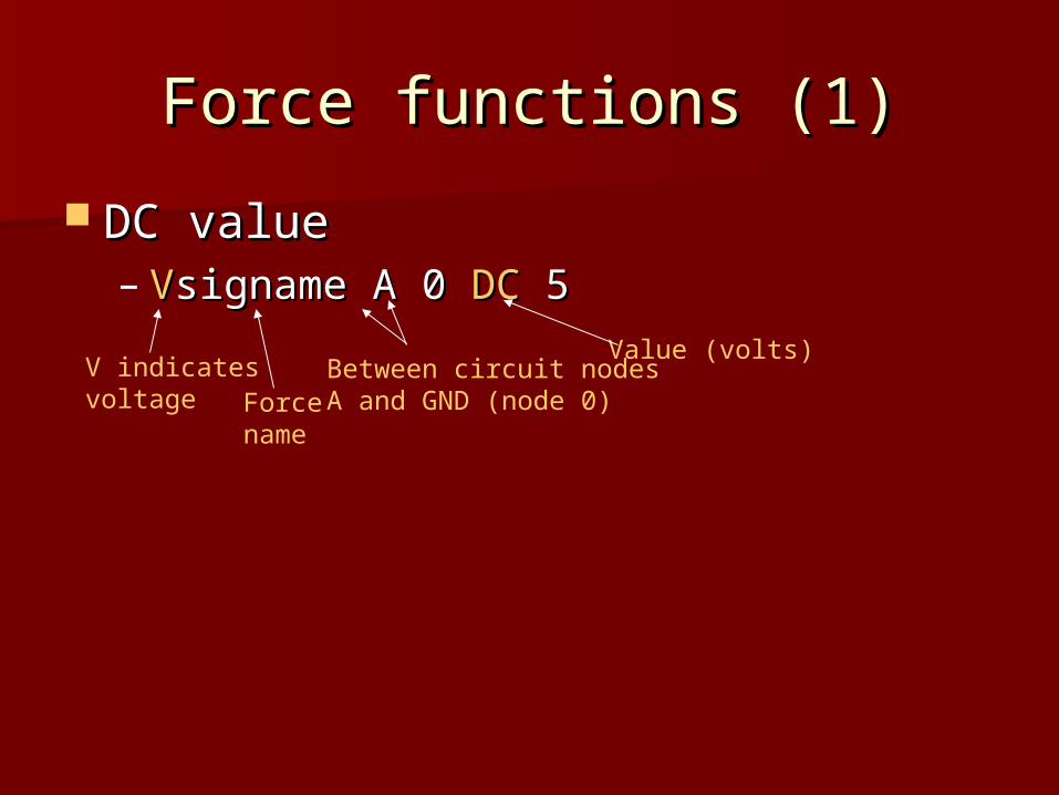
Force functions (1)Force functions (1)
DC valueDC value– VVsigname A 0 signame A 0 DCDC 5 5
Value (volts)Between circuit nodesA and GND (node 0)
V indicatesvoltage Force
name

Force functions (2)Force functions (2)
Pulse/square wavePulse/square wave– VVsigname B 0 signame B 0 pulsepulse 0 5 0 0.1N 0.1N 20N 40N 0 5 0 0.1N 0.1N 20N 40N
InitialVoltagev1
PulsedVoltagev2
Delay from start of period for waveform to begin - td
Rise Falltime timetr tf
Pulse Periodwidth tptw
v1
v2
td tr tw tf
Nodes
tp

Force functions (3)Force functions (3)
Pattern wave Pattern wave (for logic 0 & 1 values)(for logic 0 & 1 values)
VVname B 0 name B 0 patternpattern 5 0 5n 0.1n 0.1n 10n 5 0 5n 0.1n 0.1n 10n 011010 R011010 R
Logic 1 & 0voltages
Between circuit Nodes B & GND (node 0)
Bit pattern
Repeatthe pattern(optional)
Delay to waveform begin
Rise & FallTime betweenchanges Duration of
bit value
01 1
01
0
delay pattern

Eldo simulation of modulo7 Eldo simulation of modulo7 countercounter
(transient analysis)(transient analysis)

Create a std-cell based logic Create a std-cell based logic block in IC Stationblock in IC Station
Invoke: Invoke: adk_ic adk_ic In IC Station palette, select:In IC Station palette, select: Create CellCreate Cell
– Cell name: Cell name: count4count4– Attach library: Attach library:
$ADK/technology/ic/process/tsmc035$ADK/technology/ic/process/tsmc035– Process: Process: $ADK/technology/ic/process/tsmc035$ADK/technology/ic/process/tsmc035– Rules file: Rules file:
$ADK/technology/ic/process/tsmc035.rules$ADK/technology/ic/process/tsmc035.rules– Angle mode: Angle mode: 4545– Cell type: Cell type: blockblock– Select Select With connectivityWith connectivity– EDDM schematic viewpoint:EDDM schematic viewpoint: count4/layoutcount4/layout– Logic loading options:Logic loading options: flat flat

Create Cell dialog boxCreate Cell dialog box

Auto-”floorplan” the blockAuto-”floorplan” the blockplace & route > autofpplace & route > autofp

Auto-place the std cellsAuto-place the std cellsAutoplc > StdCelAutoplc > StdCel

Auto-place “ports” Auto-place “ports” (Autoplc > Ports)(Autoplc > Ports) Signal connections on cell boundariesSignal connections on cell boundaries

AutoRoute all netsAutoRoute all nets(hand-route any unrouted “overflows”)(hand-route any unrouted “overflows”)
Then: Add > Port Text to copy port names from schematic – for Calibre

Layout design rule check Layout design rule check (DRC)(DRC)
Technology-specific design rules Technology-specific design rules specify minimum sizes, spacing, etc. specify minimum sizes, spacing, etc. of features to ensure reliable of features to ensure reliable fabricationfabrication– Design rules file specified at startupDesign rules file specified at startup Ex. Ex. tsmc035.rulestsmc035.rules
From main palette, select ICrules From main palette, select ICrules – Click Click Check Check and thenand then OK OK in prompt boxin prompt box (can optionally select a specific area to check)(can optionally select a specific area to check)
– Rules checked in numeric orderRules checked in numeric order

Common errors detected by Common errors detected by DRCDRC
To fix, click on To fix, click on FirstFirst in palette to highlight first in palette to highlight first error error – Error is highlighted in the layoutError is highlighted in the layout– Click Click ViewView to zoom in to the error (see next) to zoom in to the error (see next)– Example: DRC9_2: Metal2 spacing = 3LExample: DRC9_2: Metal2 spacing = 3L– Fix by drawing a rectangle of metal2 to fill in the Fix by drawing a rectangle of metal2 to fill in the
gap between contacts that should be connectedgap between contacts that should be connected Click Click NextNext to go to next error, until all are to go to next error, until all are
fixedfixed
NOTE: There can be no DRC errors if MOSIS is NOTE: There can be no DRC errors if MOSIS is to fabricate the chip – they will run their own to fabricate the chip – they will run their own DRC.DRC.

Error: DRC9_2 metal2 spacing Error: DRC9_2 metal2 spacing = 3L= 3L
Draw rectangleof metal2to fill gap
It also called contact-to-contact metal 2 spacing DRC9_2 error

Layout vs schematic checkLayout vs schematic checkCalibre Interactive LVSCalibre Interactive LVS
From ICstation menu: From ICstation menu: Calibre > Run LVSCalibre > Run LVS– In popup, Calibre location: In popup, Calibre location: $MGC_HOME/../Calibre$MGC_HOME/../Calibre– Rules: Rules:
$ADK/technology/ic/process/tsmc035.calibre.rules$ADK/technology/ic/process/tsmc035.calibre.rules– Input: Input: count4.src.net count4.src.net (previously created in DA-IC)(previously created in DA-IC)– H-cells: H-cells: $ADK/technology/adk.hcell$ADK/technology/adk.hcell (hierarchical (hierarchical
cells)cells)– Extracted file: Extracted file: count4.lay.netcount4.lay.net
Compares extracted transistor-level netlist Compares extracted transistor-level netlist vs. netlist saved in DA-ICvs. netlist saved in DA-IC

Post-layout parameter Post-layout parameter extractionextraction
Calibre Interactive PEXCalibre Interactive PEX Extract Spice netlist, including Extract Spice netlist, including
parasitic RCparasitic RC– Simulate in Eldo or MachTASimulate in Eldo or MachTA
ICstation menu: ICstation menu: Calibre>Run PEXCalibre>Run PEX – Options similar to Calibre LVSOptions similar to Calibre LVS– Extraction options:Extraction options:
lumped C + coupling cap’slumped C + coupling cap’s distributed RCdistributed RC distributed RC + coupling cap’sdistributed RC + coupling cap’s
– Output file: count4.pex.netlistOutput file: count4.pex.netlist

Post-layout simulation with Post-layout simulation with MachTAMachTA
MachTA is an accelerated Spice simulatorMachTA is an accelerated Spice simulator– Digital & mixed-signal circuitsDigital & mixed-signal circuits– Analyze timing effects pre- and post-layoutAnalyze timing effects pre- and post-layout
SPICE netlists with parasitic R/CSPICE netlists with parasitic R/C
– Execute test vector file to verify functionalityExecute test vector file to verify functionality Algorithms support large designs Algorithms support large designs
– Partition design, simulate only partitions with Partition design, simulate only partitions with changeschanges
– Combine time-driven & event-driven operationCombine time-driven & event-driven operation– Solves linearized models using a proprietary
high-performance, graph-theory based, matrix solution algorithm

Mach TA flow diagramMach TA flow diagram
SPICEnetlist
$ADK/technology/mta/tsmc035

Prepare Calibre-extracted Prepare Calibre-extracted netlist for Mach TA netlist for Mach TA ((file.pex.netlistfile.pex.netlist))
In In file.pex.netlistfile.pex.netlist, insert model definitions and VDD/GND , insert model definitions and VDD/GND voltage source functions after comment header:voltage source functions after comment header:
* * File: m7.pex.netlistFile: m7.pex.netlist* Created: Thu Nov 15 15:25:56 2007* Created: Thu Nov 15 15:25:56 2007* Program "Calibre xRC"* Program "Calibre xRC"* Version "v2005.2_9.14"* Version "v2005.2_9.14".model n nmos.model n nmos.model p pmos.model p pmosVvdd VDD 0 5Vvdd VDD 0 5Vgnd GND 0 0Vgnd GND 0 0
Delete Delete (or comment out with * in 1(or comment out with * in 1stst column) column) .subcircuit .subcircuit statement and any continuation lines (for long statement and any continuation lines (for long statement):statement):
*.subckt modulo7 CLK Q[1] CLEARBAR I[1] Q[0] I[0] Q[2]*.subckt modulo7 CLK Q[1] CLEARBAR I[1] Q[0] I[0] Q[2] *+ L_CBAR I[2] GND VDD*+ L_CBAR I[2] GND VDD
Change Change .ends.ends to to .END.END near end of file near end of file

Post-layout simulation with Post-layout simulation with Mach TAMach TA
Invoke Mach TA:Invoke Mach TA:anaana - command file to initialize Anacad SW- command file to initialize Anacad SW
mta –ezw –t $ADK/technology/mta/tsmc035 count4.spmta –ezw –t $ADK/technology/mta/tsmc035 count4.sp
Other options:Other options:
-do file-do file (execute commands from (execute commands from file.dofile.do – instead of – instead of design.spdodesign.spdo
-donot-donot (run without simulating – compile only) (run without simulating – compile only)
-b-b (run in batch mode – no GUI – output to console) (run in batch mode – no GUI – output to console)
Transistor calibration files for this technology
Generate waveform database & display in EZwaveNetlist, modified as on previous slide
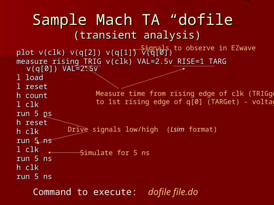
Sample Mach TA “dofile”Sample Mach TA “dofile”(transient analysis)(transient analysis)
plot v(clk) v(q[2]) v(q[1]) v(q[0])plot v(clk) v(q[2]) v(q[1]) v(q[0])measure rising TRIG v(clk) VAL=2.5v RISE=1 TARG v(q[0]) measure rising TRIG v(clk) VAL=2.5v RISE=1 TARG v(q[0])
VAL=2.5vVAL=2.5vl loadl loadl resetl reseth counth countl clkl clkrun 5 nsrun 5 nsh reseth reseth clkh clkrun 5 nsrun 5 nsl clkl clkrun 5 nsrun 5 nsh clkh clkrun 5 nsrun 5 ns
Signals to observe in EZwave
Measure time from rising edge of clk (TRIGger)to 1st rising edge of q[0] (TARGet) - voltages
Drive signals low/high (Lsim format)
Simulate for 5 ns
Command to execute: dofile file.do

EZwave waveform viewerEZwave waveform viewer(results for previous dofile)(results for previous dofile)
Double-clicksignal nameto display.

Alternative Mach TA “dofile”Alternative Mach TA “dofile”(same result as previous example)(same result as previous example)
plot v(clk) v(q[2]) v(q[1]) v(q[0])plot v(clk) v(q[2]) v(q[1]) v(q[0])measure rising TRIG v(clk) VAL=2.5v RISE=1 TARG measure rising TRIG v(clk) VAL=2.5v RISE=1 TARG
v(q[0]) VAL=2.5vv(q[0]) VAL=2.5vvpulse Vclk clk 0 pulse(0 3.3 10n .05n .05n 10n vpulse Vclk clk 0 pulse(0 3.3 10n .05n .05n 10n
20n)20n)l loadl loadl resetl reseth counth countrun 5 nsrun 5 nsh reseth resetrun 200 nsrun 200 ns
Voltage source name
Nodes to whichsource connected
v-levels delay rise fall width period
Periodic pulses

Mach TA – test vector fileMach TA – test vector file
Verify design functionality/behaviorVerify design functionality/behavior– apply test vectorsapply test vectors– capture outputscapture outputs– compare outputs to expected resultcompare outputs to expected result– vectors/outputs from behavioral vectors/outputs from behavioral
simulationsimulation Command to execute a test vector Command to execute a test vector
file:file:run –tvend tvfile.tvrun –tvend tvfile.tvtest vector file (next slide)
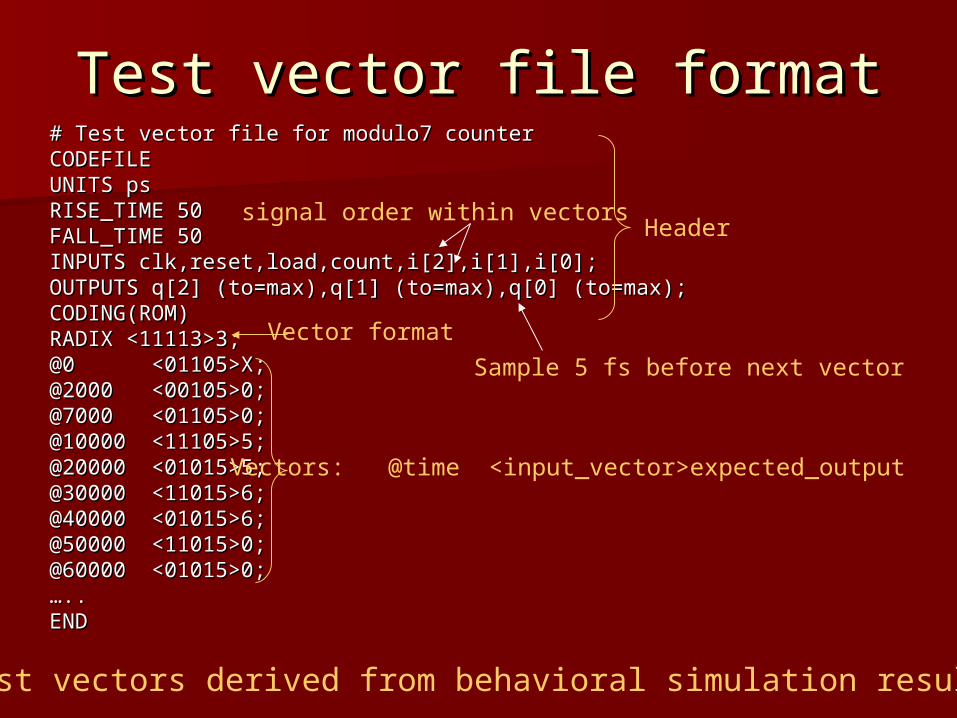
Test vector file formatTest vector file format# Test vector file for modulo7 counter# Test vector file for modulo7 counterCODEFILECODEFILEUNITS psUNITS psRISE_TIME 50RISE_TIME 50FALL_TIME 50FALL_TIME 50INPUTS clk,reset,load,count,i[2],i[1],i[0];INPUTS clk,reset,load,count,i[2],i[1],i[0];OUTPUTS q[2] (to=max),q[1] (to=max),q[0] (to=max);OUTPUTS q[2] (to=max),q[1] (to=max),q[0] (to=max);CODING(ROM)CODING(ROM)RADIX <11113>3;RADIX <11113>3;@0 <01105>X;@0 <01105>X;@2000 <00105>0;@2000 <00105>0;@7000 <01105>0;@7000 <01105>0;@10000 <11105>5;@10000 <11105>5;@20000 <01015>5;@20000 <01015>5;@30000 <11015>6;@30000 <11015>6;@40000 <01015>6;@40000 <01015>6;@50000 <11015>0;@50000 <11015>0;@60000 <01015>0;@60000 <01015>0;……....ENDEND
Header
Vectors: @time <input_vector>expected_output
Sample 5 fs before next vector
signal order within vectors
Test vectors derived from behavioral simulation results
Vector format

Behavioral simulation listing Corresponding Mach TA test vector file

Alternate test vector fileAlternate test vector file(clock generated separately by voltage (clock generated separately by voltage
source)source)
vpulse vclk clk 0 pulse(0 3.3 10n .5n .5n 10n 20n)
Can mix other simulationcommands with test vectorapplication.

Physical Design - FPGAPhysical Design - FPGA
Map to FPGA LUTs, FFs, IOBs
Place & Route
Component-Level Netlist
Configuration File
Generate Programming
Data
Xilinx “ISE”Altera “Max Plus 2”
FPGA/PLD Technology
FilesUser-SpecifiedConstraints
Simulation Model
Generate Timing Model
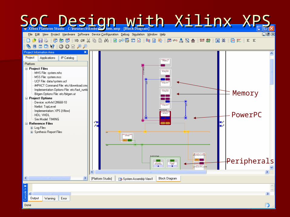
SoC Design with Xilinx XPSSoC Design with Xilinx XPS
PowerPC
Memory
Peripherals