comprehensive design analysis of thick fr-4 qfn …
TRANSCRIPT
COMPREHENSIVE DESIGN ANALYSIS OF THICK FR-4 QFN ASSEMBLIES FOR
ENHANCED BOARD LEVEL RELIABILITY
by
ABHISHEK NITIN DESHPANDE
Presented to the Faculty of the Graduate School of
The University of Texas at Arlington in Partial Fulfillment
of the Requirements
for the Degree of
MASTER OF SCIENCE IN MECHANICAL ENGINEERING
THE UNIVERSITY OF TEXAS AT ARLINGTON
August 2015

ii
Copyright © by Abhishek Nitin Deshpande 2015
All Rights Reserved

iii
To my Parents

iv
ACKNOWLEDGEMENTS
I would like to thank my advisor, Dr. Dereje Agonafer for giving me an opportunity
to work with him at EMNSPC which really shaped my career. It wouldn’t have been possible
without his valuable guidance and support throughout this work. He has always been
optimistic and encouraging me to work hard throughout my master’s degree.
I am grateful Dr. A. Haji-Sheikh for being my committee member and evaluating
my thesis work.
I am extremely thankful to Dr. Fahad Mirza who was my PhD mentor and a
committee member. He has helped me with valuable suggestions throughout my work and
academics.
I would also like to thank Mr. Alok Lohia for their expert guidance during my work
on Texas Instruments- SRC funded project, which greatly helped shape my thesis.
Special thanks to Sally Thompson, Debi Barton and Louella Carpenter who helped
me in lot of other things. I would also like to mention my lab mates Pavan, Hassaan and
Tejas who have always been there for me. You all have been really wonderful.
Last but not the least, I would like to thank my parents for being a pillar of strength
and support during the entire duration of this work.
July 27, 2015

v
ABSTRACT
COMPREHENSIVE DESIGN ANALYSIS OF THICK FR-4 QFN ASSEMBLIES FOR
ENHANCED BOARD LEVEL RELIABILITY
Abhishek Nitin Deshpande, M.S.
The University of Texas at Arlington, 2015
Supervising Professor: Dereje Agonafer
Quad Flat No-lead package (QFN) is one of the most cutting-edge technologies
emerged in the market, exhibiting high performance and efficiency with unparalleled cost
effectiveness. QFN, a leadless package, is an ideal choice for applications where size,
weight thermal and electrical characteristics are critical, particularly in mobile and handheld
devices. Applications like automotive, defense and high current circuits require the
package to be mounted on thick printed circuit boards (PCB). But using thick PCBs (>3mm)
is detrimental to the package reliability. The motivation of this work is to understand the
effect of several package parameters affecting reliability and optimize the QFN package to
improve reliability for application on thick boards. Initially, the FE modeling methodology
in ANSYS APDL was studied to gain insight on mesh/solution/analysis controls. ANSYS
APDL model was leveraged to benchmark ANSYS Workbench model in order to create a
consistent reliable model and propose best practices for modeling in ANSYS Workbench.
The material properties of the PCB were determined using Instron Micro tester, Digital
Image Correlation technique (DIC) and Thermal Mechanical Analyzer (TMA). Next, several

vi
material/dimensional parameters affecting QFN reliability on thick board were studied and
chosen for optimization. Finally, Multi design variable optimization (MDVO) was performed
to propose the optimum design parameters to reduce solder damage in thick boards QFN
assemblies.

vii
TABLE OF CONTENTS ACKNOWLEDGEMENTS .................................................................................................. iv
ABSTRACT ......................................................................................................................... v
LIST OF ILLUSTRATIONS ................................................................................................. x
LIST OF TABLES ...............................................................................................................xii
Chapter 1 INTRODUCTION ................................................................................................ 1
1.1 Quad Flat No-Lead (QFN) Packages ................................................................ 1
1.2 Thick Printed Circuit Boards .............................................................................. 2
1.3 Board Level Reliability (BLR) ............................................................................. 3
1.4 Motivation and Objective ................................................................................... 5
1.4.1 Motivation ...................................................................................................... 5
1.4.2 Goals and Objective ...................................................................................... 7
1.5 Literature Review ............................................................................................... 8
Chapter 2 MATERIAL CHARACTERIZATION.................................................................. 11
2.1 Coefficient of Thermal Expansion (CTE) ......................................................... 11
2.1.1 Digital Image Correlation Technique – CTE Measurement ........................ 12
2.1.2 CTE Results ................................................................................................ 13
2.2 Elastic Properties Measurement ...................................................................... 13
2.2.1 Instron Micro tester – Young’s Modulus Testing ......................................... 14
2.2.2 Test Results................................................................................................. 16
Chapter 3 FINITE ELEMENT MODEL AND BENCHMARKING ....................................... 17
3.1 Introduction to Finite Element Method ............................................................. 17
3.2 FEA Problem Solving Steps ............................................................................ 18
3.2.1 Geometry and Material Definition ................................................................ 19

viii
3.2.2 Meshing Model ............................................................................................ 20
3.2.3 Boundary Conditions ................................................................................... 21
3.3 Finite Element Model of QFN package............................................................ 21
3.3.1 Material Properties ...................................................................................... 22
3.3.2 Package Geometry ...................................................................................... 22
3.3.3 Loads and Boundary Conditions ................................................................. 25
3.3.4 Post-Processing .......................................................................................... 26
3.4 Benchmarking .................................................................................................. 27
Chapter 4 PARAMETRIC ANALYSIS OF QFN PACKAGE .............................................. 29
4.1 Effect of Die Size and Die Thickness .............................................................. 29
4.2 Effect of Solder Stand-off height...................................................................... 30
4.3 Effect of Center Solder under Die Pad ............................................................ 31
4.4 Effect of Solder Fillet Length ........................................................................... 31
4.5 Limits for Different Parameters ........................................................................ 32
Chapter 5 MULTI-OBJECTIVE DESIGN OPTIMIZATION ................................................ 33
5.1 Introduction to Optimization ............................................................................. 33
5.1.1 Design of Experiments (DOE) ..................................................................... 33
5.1.2 Response Surface (RS) .............................................................................. 34
5.1.3 Goodness of Fit (GOF) ................................................................................ 35
5.1.4 Predicted versus Observed Chart ............................................................... 35
5.1.5 Verification Point & Refinement Point ......................................................... 36
5.1.6 Optimization................................................................................................. 36
5.1.7 Flow Chart ................................................................................................... 37
5.2 Results and Discussion ................................................................................... 38
Chapter 6 CONCLUSION ................................................................................................. 40

ix
6.1 Summary and Conclusion ............................................................................... 40
6.2 Future Work ..................................................................................................... 41
REFERENCES .................................................................................................................. 42
BIOGRAPHICAL INFORMATION ..................................................................................... 44

x
LIST OF ILLUSTRATIONS
Figure 1-1 QFN Package Cross-section ............................................................................. 1
Figure 1-2 Cross-section of 16 Layered Board ................................................................... 2
Figure 1-3 The bathtub curve: failure rate versus time ....................................................... 3
Figure 1-4 Typical fail unit showing insufficient joint ........................................................... 6
Figure 1-5 Crack propagation in a solder joint .................................................................... 6
Figure 2-1 DIC Setup with Oven and Cameras ................................................................ 12
Figure 2-2 1. Test sample with white paint. 2. Speckled test sample ............................... 13
Figure 2-3 In-plane and out of plane CTE......................................................................... 13
Figure 2-4 PCB dogbone sample ...................................................................................... 14
Figure 2-5 Instron Micro tester .......................................................................................... 15
Figure 2-6 Elastic Modulus of PCB ................................................................................... 16
Figure 3-1 Cross section of QFN assembly ...................................................................... 23
Figure 3-2 Meshed quarter symmetry QFN package ....................................................... 23
Figure 3-3 Mesh in solder layer ........................................................................................ 24
Figure 3-4 Mesh sensitivity analysis ................................................................................. 24
Figure 3-5 Boundary conditions in quarter symmetry model ............................................ 25
Figure 3-6 Temperature cycling profile ............................................................................. 26
Figure 4-1 Graph of die size vs. ΔWavg ........................................................................... 29
Figure 4-2 Graph of die thickness vs. ΔWavg................................................................... 30
Figure 4-3 Graph of solder standoff height vs. ΔWavg ..................................................... 30
Figure 4-4 Graph of center solder vs. ΔWavg................................................................... 31
Figure 4-5 Graph of solder fillet length vs. ΔWavg ........................................................... 32
Figure 5-1 Response Surface ........................................................................................... 35

xi
Figure 5-2 Optimization Process Flowchart ...................................................................... 38

xii
LIST OF TABLES
Table 1-1 Thermal environments for electronic products ................................................... 5
Table 2-1 PCB dog bone sample dimensions .................................................................. 15
Table 4-1 Upper and lower bound limits of parameters .................................................... 32
Table 5-1 Parameters after optimization ........................................................................... 39
Table 5-2 Optimization Results ......................................................................................... 39

1
Chapter 1
INTRODUCTION
1.1 Quad Flat No-Lead (QFN) Packages
The QFN package is a thermally enhanced standard size IC package designed to
eliminate the use of bulky heat sinks and slugs. QFN is a leadless package where the
electrical contact to the printed circuit board (PCB) is made through soldering of the lands
underneath the package body rather than the traditional leads formed along the perimeter
[1]. This package can be easily mounted using standard PCB assembly techniques and
can be removed and replaced using standard repair procedures. The QFN package is
designed such that the thermal pad (or lead frame die pad) is exposed to the bottom of the
IC. This configuration provides an extremely low resistance path resulting in efficient
conduction of heat between the die and the exterior of the package (see Figure 1-1 ).
Figure 1-1 QFN Package Cross-section
Due to its superior thermal and electrical characteristics, this device package has
gained popularity in the industry during the last couple of years. Because of its compact

2
size, QFN package is an ideal choice for handheld portable applications and where
package performance is required.
For this project, the QFN packages were obtained from Texas Instruments (TI) for
analysis.
1.2 Thick Printed Circuit Boards
A printed circuit board (PCB), typically consists of alternate layers of copper and
non-conductive laminate made up of glass fiber and resin (FR4). PCBs are available in
different types based on its application E.g. Single sided (one copper and one laminate
layer), double sided (two copper layers and laminate layers), multi-layered boards. Multi-
layered boards are mainly used for high component density applications like defense and
automotive. A thick printed circuit boards (PCB) consists of large number of Cu layers (>8)
and large board thickness (>3 mm). Cross-section of a typical thick PCB with 16 copper
layers, is shown in the figure.
Solder Mask
Copper Layers
FR 4 Layers
Figure 1-2 Cross-section of 16 Layered Board
3
Primary reliability issues associated with the use of thick boards are because of
the fact that as stiffness of the PCB increases with thickness leading to less deformation
and compliance.
1.3 Board Level Reliability (BLR)
Reliability can be defined as the ability of a system or component to perform its
required functions under stated conditions for a specified period of time. To quantify
reliability, “ability” should be interpreted as a “probability”. From this definition it is clear that
all products always fail eventually. Indeed, a probability of zero failure during a certain
amount of time is physically impossible, even for integrated circuit (IC) [2].
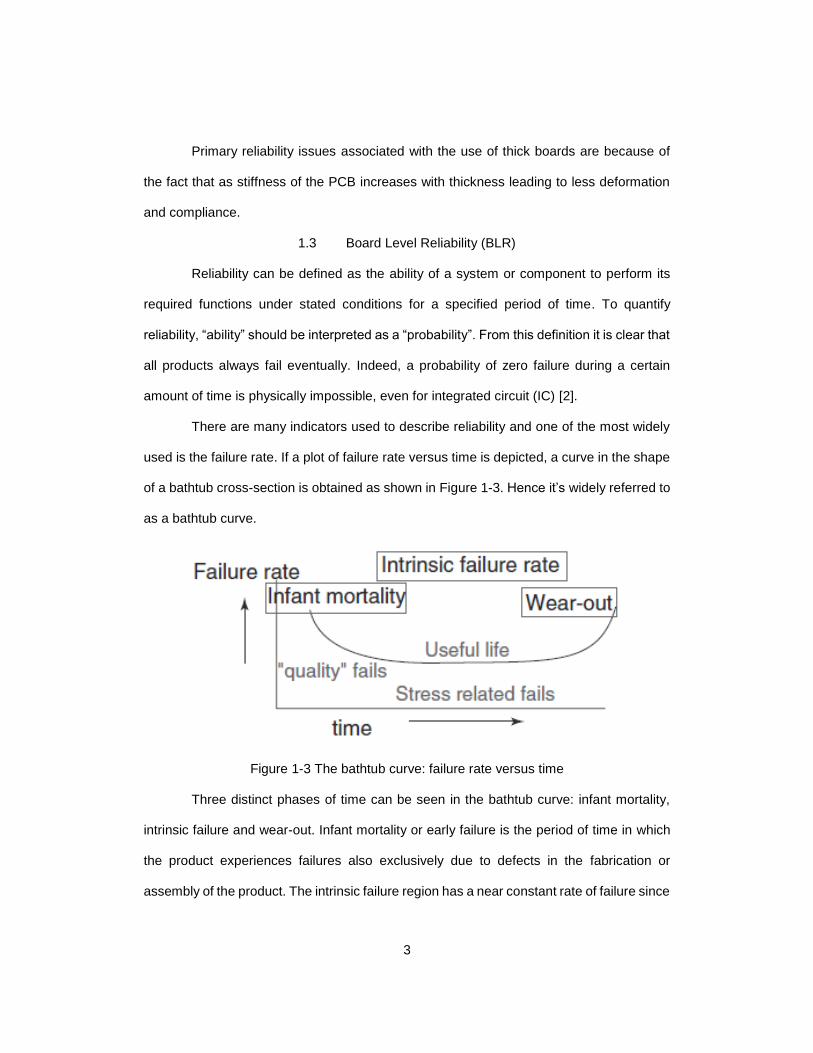
There are many indicators used to describe reliability and one of the most widely
used is the failure rate. If a plot of failure rate versus time is depicted, a curve in the shape
of a bathtub cross-section is obtained as shown in Figure 1-3. Hence it’s widely referred to
as a bathtub curve.
Figure 1-3 The bathtub curve: failure rate versus time
Three distinct phases of time can be seen in the bathtub curve: infant mortality,
intrinsic failure and wear-out. Infant mortality or early failure is the period of time in which
the product experiences failures also exclusively due to defects in the fabrication or
assembly of the product. The intrinsic failure region has a near constant rate of failure since

4
the poorly manufactured parts and defects were already screened out and eliminated and
the majority of the population left are robust product which will enjoy long and sustained
period where failures occur randomly. Finally, as the product ages, chemical, mechanical,
or electrical stresses begin to weaken the product’s performance to the point of failure. This
is called the wear-out region.
To estimate the reliability of the package, environmental stress test are used to
simulate the end use environment conditions and to uncover specific materials and process
related marginalities that may be experienced during operational life. Few consortiums
such as Joint Electronic Device Engineering Council (JEDEC) and Institute for Printed
Circuits (IPC) have adapted, documented and standardized many of the reliability tests.
Since the scope of this work is only during thermal cycling, we’ll briefly discuss about it.
Table 1-1 shows different temperature ranges for various service environments for
electronic products.
Thermal cycling is used to simulate both ambient and internal temperature
changes that result during device power up, operation and ambient storage in controlled
and uncontrolled environments. Due to difference in coefficient of thermal expansion
between various package components, they warp and expand unevenly resulting in
generation of internal thermal stresses which results in crack propagation in dielectric,
fatigue and adhesion problems. These thermo-mechanical behaviors can be detected
during thermal cycling tests. For reliability assessment, Weibull distribution is most
commonly used to accurately reflect the behavior of the product in terms of failure rate.

5
Table 1-1 Thermal environments for electronic products
Use condition Thermal excursion (°C)
Consumer electronics 0 to 60
Telecommunications -40 to 85
Commercial aircraft -55 to 95
Military aircraft -55 to 125
Space -40 to 85
Automotive-passenger -55 to 65
Automotive-under the hood -55 to 160
These reliability tests are either focused on package level or board level. Package
level or 1st level reliability tests are dedicated to the robustness of the package component
materials and design to withstand extreme environmental conditions and does not consider
the interconnects when it is mounted on board. Whereas for the board level or 2nd level
reliability tests, stresses are examined on the solder joint of the surface mount package
when mounted on board [3].
1.4 Motivation and Objective
1.4.1 Motivation
QFN package gained popularity among the industry due to its low cost, compact
size and excellent thermal electrical performance characteristics. Although QFN package
is widely used in handheld devices, some customers require it for heavy industry
application demanding thicker PCB. Literature suggests that as the thickness of PCB
increases, the reliability and fatigue life of the package decreases since the board becomes
stiffer and less flexible resulting in more transfer of stresses on the solder joint.

6
A 40 pin QFN board of thickness approx. 3 mm was tested under accelerated
thermal cycling (ATC) conditions for failure analysis (FA). The board was tested under
temperature load from -40°C to +125°C keeping the ramp and dwell time of 15min. The
tests showed that some early fails. Some of the failures were observed to have insufficient
joints, zero standoff or a combination of both (see Figure 1-4 and Figure 1-5).
Figure 1-4 Typical fail unit showing insufficient joint
Figure 1-5 Crack propagation in a solder joint

7
From the test results, it was concluded that QFN package on the thicker board fails
much earlier than thinner boards. This provides the motivation for this work. This work has
made an attempt to study different package parameters that affect QFN reliability on thick
boards, while keeping board parameters intact. The design parameters were then
optimized to mitigate failure, thus improving its reliability.
1.4.2 Goals and Objective
The primary objective of this thesis is to analyze different dimensional parameters
affecting the reliability of QFN package on thick FR4 board under ATC condition.
Understand the root cause of the solder joint failures and methods to improve the
mechanical reliability of the package thus making it to qualify the BLR industry standard for
customers use.
Initially, in order to create a confident, accurate and reliable FEA model of QFN
package, the workbench model was benchmarked with the existing TI’s APDL version.
Numerous mesh/analysis and solution controls like element size, type of elements, number
of elements, number of loadsteps/substeps, type of solver, etc. are studied for
benchmarking. The thick PCB is then characterized using Instron and DIC to determine
its elastic properties- Young’s modulus and Co-efficient of thermal expansion. In the next
step, the effect of several key package on the solder joint reliability is studied by performing
a parametric analysis. The aim is to vary the parameters in an attempt to improve the board
level reliability of the QFN package on thick FR-4 boards.
Finally, Multi Design Variable Optimization (MDVO) was performed using the
critical parameters to find optimum set of design parameters thereby increasing board level
reliability of QFN package on thick board.

8
1.5 Literature Review
One of the earliest studies on parametric analysis on QFN package was done by
Syed, et.al [4], wherein he investigated effect of package design, material parameters,
board parameters and temperature cycle condition on board level reliability of QFN
package. Based on his experiments, it was found that board level reliability is directly
dependent on CTE of mold compound. Mold compounds with lower CTE values are
detrimental to the package reliability, since lower CTE compounds have higher modulus
which makes package stiffer. It was found that exposed pad soldering critically affected
reliability. In conclusion, Syed, et.al recommended to have higher mold compound CTE
close to board CTE (~ 17 ppm/°C), lower die/package ratio (0.4 - 0.5), larger land size,
thinner printed circuit boards, soldered exposed pad and higher solder stand-off height, to
achieve excellent reliability for a micro-lead frame QFN package.
Tee et.al [5], performed a comprehensive parametric study to explore various
design parameters which affect board-level solder joint reliability of QFN package and
Power-QFN package. In his study, board-level thermal cycling tests were performed on 8
different types of QFN packages and a FEA correlation was established based on the
characteristic life data. His FEA model generated absolute fatigue life prediction within
±34% error. Along with board thickness, solder dimensions and mold compound CTE, also
assessed the effect of die thickness, lead pitch and die pad size on QFN reliability. For
enhanced solder joint reliability of QFN, Tee suggested to employ more center pad
soldering, smaller die size, thinner die, bigger die pad size, thinner board, smaller pitch,
longer lead length/width, solder with fillet, higher solder standoff, higher mold compound
CTE and smaller temperature range of thermal cycling test. Land size, mold compound
modulus and die attach material were not found to significantly affect reliability of QFN
package.

9
Wei Sun et.al [6] compared the effect of various QFN package configurations like
punch type, saw type and lead pullback type on package reliability. In addition, he also
looked at parameters which affect reliability like eutectic solder vs. lead-free solder
materials and package size. Based on the experiments, it was also concluded that
Schubert’s hyperbolic sine constitutive model could not be applied for life prediction
accurately. Hence, a new curve fitted power equation was developed which predicted life
within ±20% error.
Birzer et.al [7] performed reliability investigations under drop, bend test, power
cycling and thermal cycling, with focus on board design and soldering technology. One of
the noteworthy observation was that the QFN package mounted on board with large
number metal layers are more detrimental as compared to the same board with less
number of metal layers under thermal cycling. The entire work about parametric analysis
of QFN package and optimization, carried out in this thesis, is premised upon on the
findings by Syed, Tee, Wei Sun and Birzer.
In order to benchmark and develop a consistent and reliable finite element
modeling methodology in ANSYS Workbench, some of the past work done using ANSYS
APDL was reviewed. Bret Zahn [8] developed a viscoplastic finite element modeling
methodology using Darveaux [9] modified Anand’s constants in ANSYS APDL. He
provided good insight on various modeling tools like auto time stepping, volume averaging
technique and sub-modeling for better convergence and accuracy of the solution. The main
emphasis of his work was to create consistent modeling by using exactly same line
divisions for critical regions so that the model can be used to produce reliable results. Bret
also provided an APDL program for calculating accumulated volume averaged plastic work,
which was modified and leveraged in this work.

10
Fan et.al [10] provided a detailed discussion about the effect of different finite
element modeling techniques like global modeling, sub-modeling and sub-structure
modeling on solder joint fatigue life prediction of flip-chip BGA packages. He has also
thrown light on effect of edge singularity, volume averaging, initial stress-free condition and
choice of element type for solder joint fatigue life prediction. Some of the solution/settings
in this work are implemented based on some suggestions from Fan.

11
Chapter 2
MATERIAL CHARACTERIZATION
In order to accurately capture the material response generated in finite element
model, it is imperative to assign actual material properties for each material. Since there
is inadequate data available on the properties of thick PCB’s, in this work, thick PCBs
were characterized for finding following material properties given below-
Coefficient of Thermal Expansion (CTE)
Young’s Modulus (E)
Poisson Ratio (ʋ)
Some of the equipment’s and techniques leveraged for characterization include-
Sun Microsystems Oven with DIC
Instron Micro tester with 2kN Load Cell
2.1 Coefficient of Thermal Expansion (CTE)
Coefficient of Thermal Expansion (CTE) is defined as volumetric dilation or
contraction of a material in a particular direction as a function of the change in the
material’s bulk temperature. CTE is expressed as-
𝛼 =𝜖
𝛥𝑇
Where,
α – Coefficient of Thermal Expansion (CTE) ppm/°C
ϵ - Strain (mm/mm)
ΔT –Temperature Difference (°C)
12
Since thermal cycling load applied on the package from -40°C to 125°C in
the oven, it is necessary to know the CTE of the package so the FEA model of the
package would complement the actual condition as closely as possible.
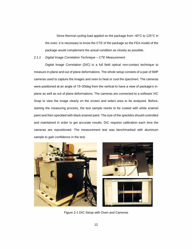
2.1.1 Digital Image Correlation Technique – CTE Measurement
Digital Image Correlation (DIC) is a full field optical non-contact technique to
measure in-plane and out of plane deformations. The whole setup consists of a pair of 5MP
cameras used to capture the images and oven to heat or cool the specimen. The cameras
were positioned at an angle of 15~20deg from the vertical to have a view of package’s in-
plane as well as out of plane deformations. The cameras are connected to a software VIC
Snap to view the image clearly on the screen and select area to be analyzed. Before,
starting the measuring process, the test sample needs to be coated with white enamel
paint and then speckled with black enamel paint. The size of the speckles should controlled
and maintained in order to get accurate results. DIC requires calibration each time the
cameras are repositioned. The measurement test was benchmarked with aluminum
sample to gain confidence in the test.
Figure 2-1 DIC Setup with Oven and Cameras
13
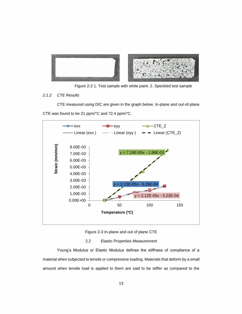
2.1.2 CTE Results
CTE measured using DIC are given in the graph below. In-plane and out-of-plane
CTE was found to be 21 ppm/°C and 72.4 ppm/°C.
Figure 2-3 In-plane and out of plane CTE
2.2 Elastic Properties Measurement
Young’s Modulus or Elastic Modulus defines the stiffness of compliance of a
material when subjected to tensile or compressive loading. Materials that deform by a small
amount when tensile load is applied to them are said to be stiffer as compared to the
y = 2.13E-05x - 5.26E-04
y = 2.12E-05x - 5.22E-04
y = 7.24E-05x - 1.96E-03
0.00E+00
1.00E-03
2.00E-03
3.00E-03
4.00E-03
5.00E-03
6.00E-03
7.00E-03
8.00E-03
0 50 100 150
Str
ain
(m
m/m
m)
Temperature (ºC)
exx eyy CTE_Z
Linear (exx ) Linear (eyy ) Linear (CTE_Z)
Figure 2-2 1. Test sample with white paint. 2. Speckled test sample

14
materials that deform by a considerable amount when tensile or compressive loading is
applied to them. Mathematically, Young’s Modulus is defined by the stress produced in a
material when some strain is applied to it.
𝐸 =𝜎
𝜖
Where,
E – Young’s Modulus (MPa)
σ – Stress (MPa)
ϵ - Strain (mm/mm)
2.2.1 Instron Micro tester – Young’s Modulus Testing
To conduct Young’s Modulus measurement tests, an Instron Micro tester of 2kN
load cell was used to apply tensile loading to the samples. An extensometer is placed on
the sample to measure strain during sample extension. The extensometer is connected to
a software to while the Instron is also connected and it gives in-situ force-displacement
graph during the test. Stress is calculated by dividing the stress from the cross-sectional
area of the sample and strain is measured using the extensometer. From the stress and
strain, Young’s Modulus is calculated for a sample.
ASTM standard was followed to prepare dog bone samples for Instron test. The
final shape of the sample is shown in the figure below
The dimensions of the sample as referred from the ASTM standards is given
below
Figure 2-4 PCB dogbone sample

15
Table 2-1 PCB dog bone sample dimensions
The test setup and procedure as shown in fig 4 was benchmarked by testing an
aluminum sample and calculating the Young’s Modulus.
Dimensions Value (mm)
L - Overall Length 100
C – Width of grip section 10
W – Width 6
A – Length of Reduced Section 32
B – Length of Grip Section 30
Dc – Curvature Distance 4
R – Radius of Curvature 6
Figure 2-5 Instron Micro tester
16
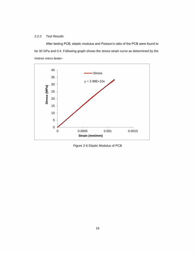
2.2.2 Test Results
After testing PCB, elastic modulus and Poisson’s ratio of the PCB were found to
be 30 GPa and 0.4. Following graph shows the stress-strain curve as determined by the
Instron micro tester-
Figure 2-6 Elastic Modulus of PCB
y = 2.98E+10x
0
5
10
15
20
25
30
35
40
0 0.0005 0.001 0.0015
Str
ess (
MP
a)
Strain (mm/mm)
Stress

17
Chapter 3
FINITE ELEMENT MODEL AND BENCHMARKING
3.1 Introduction to Finite Element Method
The Finite Element Method is a computational technique used to obtain
approximate solution to boundary value problem in engineering. FEM is virtually used in
almost every industry that can be imagined. Common application of FEA are given below.
Aerospace/Mechanical/Civil/Automobile Engineering
Structural Analysis (Static/Dynamic/Linear/Non-Linear)
Thermal/Fluid Flow
Nuclear Engineering
Electromagnetic
Biomechanics
Geomechanics
Biomedical Engineering
Hydraulics
Smart Structures
“The Finite Element Method is one of the most powerful numerical techniques ever
devised for solving differential equations of initial and boundary value problems in
geometrically complicated regions” [11]. Sometimes it is hard to find analytical solution of
important problems as they come with complicated geometry, loading condition, and
material properties. So FEA is the computational technique which helps in reaching the
satisfactory results with all the complex conditions that can’t be solved through analytical
procedure. There are wide range of sophisticated commercial code available which helps
in reaching the approximately close solution in 1D, 2D and 3D. In this FEA method, the
whole continuum is divided into a finite numbers of small elements of geometrically simple
18
shape. These elements are made up of numbers of nodes. Displacement of these nodes
is unknown and to find it, polynomial interpolation function is used. External force is
replaced by an equivalent system of forces applied at each node. By assembling the
mentioned governing equation, results for the entire structure can be obtained.
{F} = [K]{u}
Where, {F} = Nodal load/force vector
[K] = Global stiffness matrix
{u} = Nodal displacement
Structure’s stiffness (K) depends on its geometry and material properties. Load (F)
value has to be provided by user. The only unknown is displacement (u). The way in
general FEA works is, it creates the number of small elements with each containing few
nodes. There are equations known as Shape function in software, which tells software how
to vary displacement (u) across the element and average value of displacement is
determined at nodes. Those stress and/or displacement values are accessible at nodes
which explains that finer the mesh elements, more accurate the nodal values would be. So
there are certain steps that we need to follow during the modeling and simulation in any
commercial code to reach approximately true solution, which would be explained hereby
[12]. In this study commercially available FEA tool, ANSYS Workbench v15.0 has been
leveraged.
3.2 FEA Problem Solving Steps
These five steps need to be carefully followed to reach satisfactory solution to
FEA problem:
1) Geometry and Material definition
2) Defining Connection between bodies
3) Meshing the model

19
4) Defining load and boundary condition
5) Understanding and verifying the results
ANSYS is a general purpose FEA tool which is commercially available and can be
used for wide range of engineering application. Before we start using ANSYS for FEA
modeling and simulation, there are certain set of questions which need to be answered
based on observation and engineering judgment. Questions may be like what is the
objective of analysis? How to model entire physical system? How much details should be
incorporated in system? How refine mesh should be in entire system or part of the whole
system? To answer such questions computational expense must be compared to the level
of accuracy of the results that needed. After that ANSYS can be employed to work in an
efficient way after considering the following:
Type of problem
Time dependence
Nonlinearity
Modeling simplification
From observation and engineering judgment, analysis type has to be decided. In
this study the analysis type is structural; to be specific out of different other structural
problem focus in this study is on Static analysis. Non-linear material and geometrical
properties such as plasticity, contact, and creep are available.
3.2.1 Geometry and Material Definition
Geometrical nonlinearity needs to be considered before analysis. This nonlinearity
is mainly of two kinds.
1) Large deflection and rotation: If total deformation of the structure is large compared
to the smallest dimension of structure or rotate to such an extent that dimensions,
position, loading direction, change significantly, then large deflection and rotation

20
analysis becomes necessary. Fishing rod explains the large deflection and
rotation.
2) Stress Stiffening: Stress stiffening occurs when stress in one direction affects the
stiffness in other direction. Cables, membranes and other spinning structures
exhibit stress stiffening.
Material nonlinearity is also the critical factor of FE analysis, which reflects in the
accuracy of the solution. If material exhibit linear stress-strain curve up to proportional limit
or loading in a manner is such that it doesn’t create stress higher than yield values
anywhere in body then linear material is a good approximation. If the material deformation
is not within the loading condition range is not linear or it is time/temperature dependent
then nonlinear properties need to be assigned to particular parts in system. In that case
plasticity, creep, viscoelasticity need to be considered. Apart from that if structure exhibit
symmetry in geometry, then it needs to be considered when creating model of physical
structure which is advantageous in saving the computational time and expense [13]. Once
the geometry and material properties are taken care of contacts between different bodies
needs to be considered such as rigid, friction, bonded etc.
3.2.2 Meshing Model
As discussed in section 3.1, large number of mesh counts (elements) provides
better approximation of solution. There are chances in some case that excessive number
of elements increases the round off error. It is important that mesh is fine or coarse in
appropriate region and answer to that question is completely dependent on the physical
system being considered. In some cases mesh sensitivity analysis is also considered to
balance computational time with accuracy in solution. Analysis is first performed with
certain number of elements and then with twice the elements. Then both the solutions are
compared, if solutions are close enough then initial mesh configuration is considered to be

21
adequate. If solutions are different than each other than more mesh refinement and
subsequent comparison is done until the convergence is achieved [14]. There are different
types of mesh elements for 2D and 3D analysis in ANSYS which can be used based on
application.
3.2.3 Boundary Conditions
Limitations set to the problem are known as boundary condition. In order to solve
the problem these limitations are mandatory, without that the system would be assume as
a rigid body. These boundary conditions (limitations) helps software to understand where
element is likely to move and where it is restricted. In absence of boundary conditions,
system would float in space as a rigid body without deformation under acting load. So when
assuming boundary conditions, it needs to be making sure that system is constrained
enough to have deformation to prevent rigid body motion. In addition to that system should
not be under constrained or over constrained to get convergence to the solution.
3.3 Finite Element Model of QFN package
The application of FEA modeling and simulation techniques used for the QFN
package assembly is explained in this section. The ANSYS FEA procedures consist of
three steps.
1) Preprocessing: Create geometric model, elements and mesh, input material
properties.
2) Solution Process: Apply loads and boundary condition, output control, load step
control, selecting proper solver, obtaining the solution.
3) Post processing: Review the result; list the result, contour map, result animation.
Certain assumptions have been made to carry out finite element analysis.
All the parts in 3D package is assumed to be bonded to each other

22
Temperature change in package during thermal cycling is assumed to be same
throughout the package
Except solder bump, all other materials are assumed to behave as linear elastic
3.3.1 Material Properties
Material properties used for FE model were linear elastic properties for copper
pads/ lead frame, die, mold compound and solder mask. Linear orthotropic elastic
temperature dependent properties were used for PCB. SAC305 Solder was modeled as
rate-dependent viscoplastic material using Anand’s viscoplastic model, which takes into
consideration both creep and plastic deformations to represent the secondary creep of
solder. Through its material constants A, Q, ξ, m, n, h0, a, s0, ŝ, which are determined by
curve-fitting the experimental data, Anand's law accounts for solder's strain-rate and
temperature sensitivity. Anand’s viscoplasticity model for solder can be described as
follows- [15]
𝑑𝜀𝑝
𝑑𝑡= 𝐴 sinh (𝜉
𝜎
𝑠)
1𝑚exp(−
𝑄
𝑘𝑇)
With the rate of deformation resistance equation-
ṩ = [ℎ0(|𝐵|)𝛼𝐵
|𝐵|]𝑑𝜀𝑝
𝑑𝑡
Where,
𝐵 = 1 −𝑠
𝑠∗
And
𝑠∗ = ŝ [1
𝐴
𝑑𝜀𝑝
𝑑𝑡𝑒𝑥𝑝 (−
𝑄
𝑘𝑇)]
𝑛
3.3.2 Package Geometry
A 3D 6 x 6mm QFN package was modeled in ANSYS v15.0 using the package
drawings and optical microscope images. Figure 3-1 shows the cross-sectioning of the
QFN package.
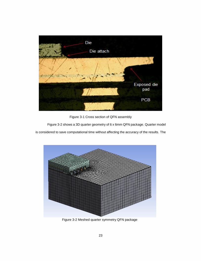
23
Figure 3-1 Cross section of QFN assembly
Figure 3-2 shows a 3D quarter geometry of 6 x 6mm QFN package. Quarter model
is considered to save computational time without affecting the accuracy of the results. The
Figure 3-2 Meshed quarter symmetry QFN package

24
model was discretely meshed using different meshing option in ANSYS Workbench v15.0.
Mesh refinement and mesh sensitivity analysis was performed to reach maximum accuracy
with optimum solution time.
Figure 3-3 Mesh in solder layer
0.324
0.326
0.328
0.33
0.332
4 0 K 5 5 K 7 5 K 8 0 K
ΔW
(M
# OF ELEMENTS
M E S H S E N S I T I V I T Y A N A L Y S I S
Figure 3-4 Mesh sensitivity analysis

25
3.3.3 Loads and Boundary Conditions
Boundary conditions imposed on the global model can be seen in Figure 3-5.
Symmetry boundary conditions are applied to the two boundary planes of the quarter
symmetry model. The center node is fixed to prevent rigid body motion.
Thermal cycling load of -40°C to 125°C ;15 min ramp/dwell was applied on the
model as shown in the following Figure 3-6.Simulations are done over three complete
cycles since most of the solder joints have reached a stable state after the end of third
cycle. The initial stress-free temperature was set to be the maximum temperature in the
cycle. Choosing the high dwell temperature of the BLR test as the stress-free temperature
helps the system to reach the stabilized state faster.
Symmetry
Node Constrained in Z direction
Symmetry
Figure 3-5 Boundary conditions in quarter symmetry model

26
3.3.4 Post-Processing
Since solder is viscoplastic in nature, stress or strain based damage parameter
may be accurate to quantify solder joint fatigue life. Hence, volume averaged plastic work
accumulated between 3rd and 2nd cycle (ΔWavg) is used a damage parameter. The results
are volume averaged over 25µm layer thickness to minimize the effect of stress
singularities in the model. This damage parameter is then later used in parametric analysis
and optimization.
An APDL code was modified and leveraged in Workbench to be used for
optimization as follows-
set,8,last,1
cmsel,s,solderloc,elem
etable,vo3table,volu
etable,vse3table,nl,plwk
Figure 3-6 Temperature cycling profile

27
smult,pw3table,vo3table,vse3table
ssum
*get,splwk,ssum,,item,pw3table
*get,svolu,ssum,,item,vo3table
pw3=(splwk/svolu)
W= pw3-pw2
3.4 Benchmarking
An FEA model to be reliable, accurate and to gain confidence in modeling, it needs
to be benchmarked before using for solder joint fatigue life prediction. Therefore, a
thorough study about the effect of different types of meshing methods, analysis/ solution
controls was performed and later included in the workbench model used in this work.
Some of the key conclusions of the study which were included in the model are as
follows-
1) Stress-free temperature - There are most commonly three types of stress free
temperatures used in these analyses. First one is the melting temperature of solder
approx. 200°C which assumes that solder starts providing mechanical support as
soon as it solidifies. Second condition assumes that solder undergoes stress
relaxation during storage and hence the stress free temperature is 25°C. Third
condition assumes that solder is stress free at highest temperature (125°C) in the
thermal cycle. Fan [10] demonstrated that use of high thermal cycling temperature
as stress-free temperature leads to attain quickly stabilized strain energy density
solutions which in turn significantly increases computational efficiency. Therefore,
stress-free temperature of 125°C was chosen in this work.

28
2) Identical mesh (line divisions) in all solder volumes – It is imperative to provide
identical mesh size/ divisions and element type in all the solder volumes on the
periphery of the package to achieve consistent and accurate results. In this work,
solder volume lines were divided as 8, 5 and 5 along its length, width and height.
3) Sub-steps - It is observed during the study that time discretization affects accuracy
of the results. As the time divisions go on reducing, the solution reaches accuracy.
But increasing time divisions, increases solution times tremendously which makes
it computationally inefficient. To overcome this problem, it is suggested to provide
identical time divisions for each load step. In this study, all load steps are divided
into 10 sub-steps.
4) Iterative solver used as opposed to direct solver – Iterative solver like
Preconditioned Conjugate Gradient (PCG) solver is recommended for large
models consisting of solid elements and fine mesh [14]. PCG solver is most robust
solver, whereas direct solver is mostly recommended for small DOF linear
analysis. Therefore, in this work PCG solver was used.
5) Large Deflection ‘ON’ and Rate ‘ON’ – These ANSYS commands are used in order
to activate the effect of non-linear geometry and to include creep effect in the
analysis.
6) Maintain equal thickness of critical solder layer for calculating plastic work – As the
thickness of the solder regions on which the volume averaged accumulated plastic
work (ΔWavg) is increased, the value of ΔWavg decreases. Hence, for consistent
and accurate results, it is important to use same thickness layer for ΔWavg
calculation. In this study, 25µ thick solder layer was chosen for calculating ΔWavg.

29
Chapter 4
PARAMETRIC ANALYSIS OF QFN PACKAGE
In this design study, the effect of some of the key package parameters such as
package geometry and material properties are investigated in an attempt to improve the
solder joint reliability of the QFN. The parameters in focus are Die size, Die thickness,
Solder stand-off height, Solder fillet length and Center solder under die pad. Only one
package parameter is modified at a time to study its effect on the solder joint reliability. The
analysis is done on QFN package with the same material properties but on thick board.
The main objective is to study the effects on these key parameters on the solder
joint fatigue life to support package design for reliability in different applications.
4.1 Effect of Die Size and Die Thickness
Selecting smaller die size and die thickness is better for reliability because the die
edge is farther from the peripheral solder joint thus resulting in less local CTE mismatch.
1.5
2
2.5
3
3.5
4
4.5
0.29 0.3 0.31 0.32 0.33
Die
siz
e (m
m)
ΔW (MPa)
Figure 4-1 Graph of die size vs. ΔWavg

30
4.2 Effect of Solder Stand-off height
Generally, higher solder stand-off height has longer fatigue life. The larger solder
thickness helps to reduce the plastic work induced during thermal cycling. Also, more
solder volume means more resistance to the crack propagation in the solder joint.
0.03
0.04
0.05
0.06
0.07
0.08
0.09
0.2 0.3 0.4 0.5
Sold
er H
eigh
t (m
m)
ΔW (MPa)
0.09
0.14
0.19
0.24
0.29
0.3245 0.325 0.3255 0.326 0.3265 0.327 0.3275
Die
Th
ickn
ess
(mm
)
ΔW (MPa)
Figure 4-2 Graph of die thickness vs. ΔWavg
Figure 4-3 Graph of solder standoff height vs. ΔWavg

31
4.3 Effect of Center Solder under Die Pad
Amount of center pad soldering affects QFN reliability on thick board. As much
as, 40% decrease in reliability is observed when there’s no solder under die pad. This is
associated with the reduced amount of solder volume thereby providing less support to
the package.
4.4 Effect of Solder Fillet Length
More solder length has more solder volume and hence more solder available to
absorb the damage. This strengthens the critical solder joint. The effect of different solder
fillet length on plastic work is shown in the graph below
1.5
2
2.5
3
3.5
4
4.5
5
0.324 0.325 0.326 0.327 0.328 0.329
Cen
ter
Sold
er (
mm
)
ΔW (MPa)
Figure 4-4 Graph of center solder vs. ΔWavg

32
4.5 Limits for Different Parameters
Based on the parametric analysis and literature review, following parameters with
their upper and lower limits, were chosen for optimization-
Table 4-1 Upper and lower bound limits of parameters
Parameter Limit (mm)
1 Solder dimensions 2 - 4.5
2 Solder fillet length 0.15 - 0.19
3 Solder standoff height 0.05 - 0.08
4 Die size 2.5 - 4.5
5 Die thickness 0.15 - 0.25
0.12
0.13
0.14
0.15
0.16
0.17
0.18
0.19
0.2
0.315 0.32 0.325 0.33 0.335 0.34 0.345
Sold
er F
illet
Len
gth
(m
m)
ΔW (MPa)
Figure 4-5 Graph of solder fillet length vs. ΔWavg

33
Chapter 5
MULTI-OBJECTIVE DESIGN OPTIMIZATION
5.1 Introduction to Optimization
As it is known that a good design point is often the trade-off between various
objectives, exploration cannot be done by using an optimization algorithm which leads to
one design point.
It is important to gather information within the applicable design space to answer
all kind of “what if” question. To gather all this information and efficiently reach the final
design point, ANSYS Workbench has “Design Exploration” optimization tool. Design
exploration describes the relationship between the design variables and the performance
of the product by using Design of Experiments (DOE), combined with response surfaces.
DOE and response surfaces provide all of the information required to achieve Simulation
Driven Product Development [16].
5.1.1 Design of Experiments (DOE)
Design of Experiment is the technique to scientifically determine location of
sampling points within the available design space to cover as much as possible space.
There is wide range of algorithm available in engineering literature which tries to locate the
sampling points such that design space for input parameters is explored in most efficient
way. In ANSYS within the design exploration tool there are 7 different algorithms available
which helps in generating DOE within specified design space (specified by upper and lower
bound) for each input parameters, which are mentioned below [16].
1) Central Composite Design (CCD)
2) Optimal Space-filling Design (OSF)
3) Box-Behnken Design
4) Custom

34
5) Custom + Sampling
6) Sparse Grid Initialization
7) Latin Hypercube Sampling Design (LHS)
In this study Custom + Sampling DOE was considered. Sampling design points
were leveraged from Optimal Space-filling Design algorithm and extreme combination of
design space were added as a custom points.
5.1.2 Response Surface (RS)
The Response Surfaces are functions where the output parameters are described
in terms of the input parameters. This input and output values are taken from solved DOE.
They are built from the Design of Experiments in order to provide quickly the approximated
values of the output parameters, everywhere in the analyzed design space, without to
perform a complete solution. The accuracy of a response surface depends on factors such
as complexity of the variations in the solution, number of design points and type of
response surface selection. To create response surface through DOE there are certain
meta-models available in design exploration tool which are mentioned below [16].
1) Standard Response Surface – Full 2nd Order Polynomial
2) Kriging
3) Non-Parametric Regression
4) Neural Network
5) Sparse Grid
In this study Non-Parametric Regression meta-model has been used. This
algorithm covers the predictably high nonlinear behavior of output with respects to its input.
Response surface for both output parameters considered in this optimization study is
shown in figure.

35
5.1.3 Goodness of Fit (GOF)
Goodness of Fit is an evaluation parameter for response surface which helps you
determine how well your response surface is fitting all the design points in design space.
To determine the accuracy of current response surface GOF is used. To check the
acceptability of GOF various parameters are there in GOF matrix which will be discussed
here. If GOF is not acceptable that means current response surface is not accurately
representing a parametric model. In that case there is need to refine your response surface
[16].
5.1.4 Predicted versus Observed Chart
This chart represents for output parameters the value predicted from response
surface versus the value observed from design points. Closer the points from the diagonal
identity line, better the response surface fit all points. All the output values are by default
normalized [16].
Plastic w
ork
Figure 5-1 Response Surface

36
5.1.5 Verification Point & Refinement Point
Initial response surface is built from design points available in DOE. As this
response surface is built from limited number of design points, it needs a check for
accuracy. RS algorithms are mainly an interpolation process which fits all the design points
(such as kriging). In this case GOF parameters would indicate that response surface is
accurate enough for given design points but does not indicate that current RS represents
whole parametric solution. A better way to check this accuracy is creating a verification
points. Verification points are solved on real model and their output is compared with
predicted output from the current RS to check the accuracy of RS. To check the fitness of
this verification points with current RS, there is a different GOF matrix for verification points
with the same criteria. To quickly determine that, predicted versus observed chart can be
used. It is easy to differentiate original design points (square) with verification point (round)
on this chart.
Through GOF matrix of verification points and predicted versus observed chart
accuracy of current RS can be obtained. If this it’s not acceptable, that means current RS
need a refinement to improve accuracy and covering parametric solution. So idea is to add
those verification points as a refinement points to refine current RS. In RS project window
there is option of inserting these verification points as refinement points which lets you
refine and update response surface [16].
5.1.6 Optimization
In Design Exploration tool there are two options to perform Goal Driven
Optimization (GDO): Response surface optimization and direct optimization. Direct
optimization is single component system which uses a real solve while response surface
optimization depends on its own response surface to provide optimized candidate, so
accuracy of optimized candidate depends on accuracy of RS. In this study response

37
surface optimization technique was used to perform optimization. There are several
algorithms available for performing this optimization such as screening, Multi-Objective
Genetic Algorithm (MOGA), Nonlinear Programming by Quadratic Lagrangian (NLPQL),
and Mixed-Integer Sequential Quadratic Programming (MISQP).
In this study screening algorithm has been considered to perform optimization. It
allows us to create new numbers of samples and then sort them by using objective function
or constrains.
In this algorithm you can enter as much number of samples you want as it does
not take much time. This method is RS based, so no need of real solve. After that you get
a chance to specify your objective for optimization and constrains, if any. In case of multiple
objectives, you can provide weight (preference) to each one by defining higher or lower
relevance. You also get an option of how many optimized candidate you want. There is
also an option of verifying optimized candidate with verification point with real solve. If the
difference between both points is not acceptable then again refinement can be done [16].
5.1.7 Flow Chart
Optimization process in ANSYS contains of different individual steps like creating
DOE, RS, perform GOF check, verifying accuracy of current RS and then perform
optimization as well verify the optimized candidate which follows the below mentioned flow
chart.
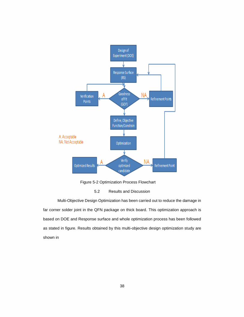
38
5.2 Results and Discussion
Multi-Objective Design Optimization has been carried out to reduce the damage in
far corner solder joint in the QFN package on thick board. This optimization approach is
based on DOE and Response surface and whole optimization process has been followed
as stated in figure. Results obtained by this multi-objective design optimization study are
shown in
Figure 5-2 Optimization Process Flowchart

39
Table 5-1 Parameters after optimization
Optimized Parameters (mm)
Solder Dimension 4.2 x 3
Solder Fillet Length 0.18
Solder Standoff Height 0.076
Die Size 3.8
Die Thickness 0.2
Table 5-2 Optimization Results
Cases Normalized Plastic
Work % Change
1 Baseline 1 -
2 Optimized candidate
points 0.87 -13
It is observed from the above Table 5-2 that normalized plastic work for
optimized candidate points has been improved by 13% as compared to baseline design
parameters thereby increasing reliability.

40
Chapter 6
CONCLUSION
6.1 Summary and Conclusion
In this work, a 3D finite element model for QFN package was analyzed to assess
the board level reliability under thermal cycling and perform MDVO to increase reliability.
The work was divided in four sections. First section involved understanding various
meshing, analysis/solution controls to benchmark the FE model in ANSYS workbench with
TI’s ANSYS APDL model. Benchmarking was necessary to create a reliable and accurate
modeling methodology. In benchmarking process, it was observed that factors such as
stress-free temperature, number of sub-steps, type of solver, type of mesh and thickness
of solder layer used for calculating plastic work are the ones which affect volume averaged
accumulated plastic work values.
Material characterization of PCB was performed using Instron micro-tester and
Digital Image Correlation technique in the second section. All the measurement tests were
first benchmarked with Al sample and results were found to be in close agreement. The in-
plane Young’s modulus and Poisson’s ratio was found to be 30 GPa and 0.4, while in-plane
and out-of-plane co-efficient of thermal expansion were 21 ppm/°C and 72.4 ppm/°C.
Anand’s viscoplastic constitutive law was used to describe the inelastic behavior of the
lead-free solder alloy.
In the third section, a parametric design analysis was performed on QFN package
mounted on thick FR-4 board to understand the effect of each parameter on reliability of
the package. It was concluded that for better reliability it is recommended to have smaller
die size and die thickness, larger solder stand-off height and longer solder fillet length.
Based on the parametric analysis, lower bound and upper bound limits were chosen for
each parameter which is later used in MDVO.

41
Finally, based on the parameter limits, a design of experiments (DOE) was
explored to capture the effect of maximum possible design points on plastic work. Next, a
response surface was created using the DOE and MDVO was performed to determine
optimum set of design points which minimized the accumulated volume averaged plastic
work in the critical solder joint by 13%, hence increasing reliability.
6.2 Future Work
The aim of this work was to develop a reliable FEA modeling methodology and
optimize key package parameters to increase solder joint fatigue life under accelerated
thermal cycling. Some of the recommendations in this work can be validated experimentally
be performing accelerated thermal cycling test in environmental chamber. Similarly, solder
joint fatigue life of QFN package subjected to power cycling loads can be investigated
computationally and experimentally.
Also, on FEA modeling standpoint, work can be done to create a robust reliable
mesh independent model which can be used for solder joint fatigue analysis for different
types of asymmetric packages. This can reduce meshing and benchmarking time for new
models in ANSYS workbench.

42
REFERENCES
[1] Y. B. Quek, "QFN Layout Guidelines," Texas Instruments, Dallas, 2006.
[2] G. Q. Zhang, Mechanics of Microelectronics, XIV ed., Springer, 2006.
[3] R. Rodgers, "Cypress Board Level Reliability Test for Surface Mount Packages," 2012.
[4] A. Syed and W. Kang, "Board Level Assembly and Reliability Consideration for QFN Typer Packages," Chandler, AZ, 2003.
[5] T. Y. Tee, H. S. Ng, D. Yap and Z. Zhong, "Comprehensive board-level solder joint reliability modeling and testing of QFN and PowerQFN packages," Microelectronics Reliability, vol. 43, no. 8, 2003.
[6] W. Sun, W. H. Zhu and R. Danny, "Study on the Board level SMT Assembly and Solder Joint Reliablity of Different QFN Packages," in EuroSimE IEEE, London, 2007.
[7] C. Birzer and S. Stoeckl, "Reliablity investigations of leadless QFN packages until end-of-life with application-specific board stress-tests," in ECTC, San Diego, 2006.
[8] B. Zahn, "Finite Element Based Solder Joint Fatigue Life Predictions for a Same Die Stacked Chip Scale Ball Grid Array Package," in Electronics Manufacturing Technology Symposium, 2002.
[9] R. Darveaux, "Effect of Simulation Methodology on Solder Joint Crack Growth Correlation," in ECTC, Las Vegas, NV, 2000.
[10] X. Fan, M. Pei and P. Bhatti, "Effect of finite element modling techniques on solder joint fatigue life prediction of flip-chip BGA packages," in ECTC, 2006.
[11] J. N. Reddy, An Introduction to the Finite Element Method, 3 ed., McGraw-Hill, 2005.
[12] T. Raman, "Assessment of the mechanical Integrity of Cu/Low-K dielectric in a Flip Chip package," UT Arlington, Arlington, 2012.
[13] E. Madenci, The Finite Element Method and Applications in Engineering Using ANSYS, Springer, 2007.
[14] "ANSYS Documentation, Release 15.0," 2014. [Online]. Available: http://www.ansys.com.

43
[15] J. Zhao, V. Gupta, A. Lohia and D. Edwards, "Reliability Modeling of Lead-Free Solder Joints in Wafer-Level Chip Scale Packages," Journal of Electronic Packaging, vol. 132, no. 1, p. 6, March 2010.
[16] Workbench Design Exploration User Guide, ANSYS, 2015.

44
BIOGRAPHICAL INFORMATION
Abhishek Deshpande received his Bachelor’s degree in Mechanical Engineering
from the University of Pune in the June 2012. He then worked for Anveshak Technology
and Knowledge Solutions, Pune as a Design Engineer for 1 year, from September 2012 to
July 2013. He later pursued Master’s in Mechanical Engineering at University of Texas at
Arlington in Fall 2013. At UTA, he worked at the Electronics MEMS & Nanoelectronics
Systems Packaging Center (EMNSPC) under Dr. Dereje Agonafer and developed a keen
interest in reliability and failure analysis of electronic packages. His research interest
includes reliability, fracture mechanics, thermo-mechanical simulation and material
characterization. He was an integral part of the SRC funded project where he worked
closely with the industry liaisons. Upon graduation, Abhishek plans to pursue a doctorate
degree in mechanical engineering at University of Maryland, College Park.