compound semiconductor - institute of physicsdownload.iop.org/cs/cs_13_11.pdf · · 2007-11-28si...
TRANSCRIPT

CompoundSemiconductor
month 2007 Volume 13 number X
C o n n e C t i n g t h e C o m p o u n d S e m i C o n d u C t o r C o m m u n i t y
xxxxxxx
Xxxxxxxxxxxxxxx xxxxxxxxxxx xxxxxxxxxxxxx
Headline news TecHnology conference reporT
RFMD outlines new strategy following Sirenza deal p5
economies of scaleSkyworks saves thousands of dollars by cutting photoresist volumes. p14
Hybrid solutiontoyota pledges to use Sic in “ultimate ecovehicle”. p17
CompoundSemiconductor
december 2007 Volume 13 number 11
C o n n e C t i n g t h e C o m p o u n d S e m i C o n d u C t o r C o m m u n i t y
LedS
MOCVD order boom as new LED ramp beckons
CSDec07Cover.indd 1 20/11/07 14:27:45

Our leading
technology.
For highest
quality in
your products.
AIXTRON AG · Kackertstraße 15–17 · 52072 Aachen, Germany · www.aixtron.comSI G
rou
p G
mb
H, W
etzl
ar, G
erm
any
Innovators in production of highly complex
materials use cutting edge technology!
Our CVD systems with highest performance
and best economy.
push yourPERFORMANCE
AIXT Anzeige 213x282 RZ 08.09.2006 13:44 Uhr Seite 1

Compound Semiconductor December 2007 compoundsemiconductor.net �
Compound Semiconductor’s circulation figures are audited by BPA International
C o n n e C t i n g t h e C o m p o u n d S e m i C o n d u C t o r C o m m u n i t y
induStry
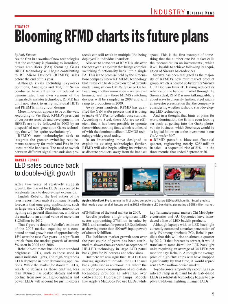
Headline News: Blooming RFMD charts its future plans…LED sales bounce back to double-digit growth.
The Month in RFICs: TriQuint prospects excite Quinsey…Tegal delivers its first net profit since 2000…Skyworks moves to 6 inch wafers…Swedish TranSiC is first with power switch.
The Month in HB-LEDs: Nichia and Seoul spat deepens…Cash-rich Cree eyes acquisitions…Kingbright told to destroy its LEDs.
The Month in Optoelectronics: System builders get concentrators qualified…Car makers spur on IPG…US awards $21.7 m solar funds.
Portfolio: Aixtron continues its upward march An entrenched position in the MOCVD equipment sector and the continued surge in demand for tools from LED manufacturers made Aixtron’s stock one of the hottest investments in a tumultuous year on the exchanges.
5
6
8
�0
�2
teChnology
Photoresist cuts strengthen Skyworks’ gross margin: Six Sigma analysis has driven cuts in Skyworks’ photoresist consumption and has resulted in annual savings in excess of $450,000, according to Jens Riege.
SiC readies itself to save the world: But can the industry’s businesses save themselves as they compete with each other in a tight niche for limited sales to final consumers? Andy Extance was in Otsu, Japan, to document the aspirations and growing pains, as well as the latest research on show in this maturing field at ICSCRM 2007.
Product Showcase
TriQuint joins the integration game: TriQuint Semiconductor has united its HBTs and PHEMTs with a BiHEMT process that promises to integrate power amplifiers and antenna switches on the same chip, according to Tim Henderson.
Rings speed wavelength switching: Micro-ring full-band tunable lasers can deliver fast and stable wavelength switching. This makes them the ideal candidate for next-generation networks employing optical packet-switching technology, say Shinji Matsuo and Toru Segawa from NTT Photonics Laboratories, Japan.
Research Review: Dots deliver phosphor-free white light…UCSB ramps non-polar blue LED output power.
�4
�7
�9
2�
25
28
Opening upAnadigics CEO Bami Bastani has revealed why the RFIC maker missed its latest quarterly profit target, despite over-achieving on sales. p7
D e c e m b e r 2 0 07V o l u m e 1 3N u m b e r 11
AnAD
IgIC
S
Single-chip solutionTriQuint is addressing the demand for smaller devices with greater functionality with a BiHEMT process that combines HBTs and PHEMTs on one chip. p21
TRIQ
uIn
T
Beijing nightsCree will supply high-brightness LEDs to light up the Olympic swimming pool at next year’s Beijing games. p9
CREE
Main cover image: Aixtron and Veeco are witnessing a sustained increase in orders for MOCVD equipment, as LED epiwafer manufacturers prepare themselves for a ramp in production. This image shows a non-polar InGaN/GaN emitter developed by US researchers. See pp 12 and 28. Credit: UCSB.
CSDec07Contents.indd 1 20/11/07 14:28:43

compoundsemiconductor.net December 2007 Compound Semiconductor2
e d i t o r i a l
Editor Michael [email protected] +44 117 930 1013. Fax +44 117 925 1942
Features editor Richard [email protected] +44 117 930 1192
Reporter Andy [email protected] +44 117 930 1007
Senior sales executive David [email protected] +44 117 930 1032. Fax +44 117 920 0977
Business development manager Rosemarie [email protected] +1 215 627 0880. Fax +1 215 627 0879
Sales executive Paul [email protected] +1 215 627 0880
Marketing executive Amanda [email protected] +44 117 930 1165. Fax +44 117 920 0984
Publisher Nicola GulleyProduction Louise UnwinAd production Mark TrimnellArt director Andrew GiaquintoTechnical illustrator Alison Tovey
SubscriptionsAvailable free of charge to qualifying individuals working at compound semiconductor fabs and foundries. For further information visit compoundsemiconductor.net/subscribe. Subscriptions for individuals not meeting qualifying criteria: individual £90/$165 US/€135; library £199/$360 US/€290. Orders to: Compound Semiconductor, WDIS, Units 12 & 13, Cranleigh Gardens Industrial Estate, Southall, Middlesex UB1 2DB, UK. Tel +44 208 606 7518; Fax +44 208 606 7303. General enquiries: [email protected].
9094 average total qualified circulation**June 2007 BPA audit statement
Editorial boardMayank Bulsara Atlas Technology (USA); Andrew Carter Bookham Technology (UK); Jacob Tarn OCP/Gigacomm (Taiwan); Ian Ferguson Georgia Institute of Technology (USA); Toby Strite JDSU (USA); Mark Wilson Motorola (USA); Dwight Streit Northrop Grumman (USA); Joseph Smart Crystal IS (USA); Colombo Bolognesi Swiss Federal Institute of Technology (Switzerland); Shuji Nakamura University of California at Santa Barbara (USA)
©2007 IOP Publishing Ltd. All rights reserved.
US mailing information: Compound Semiconductor (ISSN 1096-598X) is published 11 times a year for $165 by IOP Publishing, Dirac House, Temple Back, Bristol BS1 6BE, UK. Periodicals postage paid at Middlesex, NJ 08846. POSTMASTER: send address corrections to Compound Semiconductor, c/o PO Box 177, Middlesex, NJ 08846. US agent: Pronto Mailers Association Inc, 200 Wood Avenue, PO Box 177, Middlesex, NJ 08846.
Giants’ steps
Aixtron AG IFCApplied Energy Systems Inc 9Bandwidth Semiconductor 6EpiNova GmbH – III/V-Epitaxial Solutions 27Gatan UK 19Laser Photonics LLC 7MicroChem 20
Oerlikon 8PIDA (Photonics Industry and Technology Development Association) 4Raboutet 11Riber 13Rohm and Haas Electronic Materials 10Veeco Turbo Disc OBC
Advertisers’ Index
If you asked somebody at random to name a semiconductor company, the chances are most people would say: “Intel”. Now, there aren’t really any compound semiconductor companies that make for household names (yet), but if you had to pick the “Intel” of the GaAs world, there’s a fair chance that you’d say: “RF Micro Devices”.
These two firms are the kingpins in silicon and GaAs semiconductors. One thing that really characterizes them is their commitment to research and the development of new transistor technologies. It is, after all, Intel’s Gordon Moore whose eponymous “law” is most closely associated with the forward march of semiconductor performance.
Intel is not one for resting on its laurels. Months ahead of its rivals, it has just become the first to launch commercial designs based on the 45 nm technology “node”. These designs are revolutionary transistors featuring metal gates and a high-k gate dielectric based on the rare element hafnium – a feat that Moore himself regards as the biggest
change in transistor technology in four decades.Down at RFMD, there are parallels. The
Greensboro firm, which was the first to really exploit the GaAs HBT in cell phone handsets, has been secretly working on a BiFET process,
and what it describes as a revolutionary GaAs transistor. GaN HEMTs are also set for volume production and we await further details with interest.
What’s noticeable about the way in which Intel now promotes itself is the importance placed on materials, something that the compounds industry has inevitably focused on as a matter of course. Go to the Intel webpages covering 45 nm technology and you’ll be assailed with the section of the periodic table in which hafnium resides.
Beyond 2009, Intel might just be taking a closer look at groups III and V. In fact, its researchers already are – with a view to using compound semiconductor transistors around the middle of the next decade.
This convergence of silicon and compound semiconductors will be one of the critical industry themes under discussion at our 2008 Key Conference, for which we’re heading back to the Florida Keys for the first time in five years. Mike Mayberry, Intel’s director of components research, is presenting a keynote talk at the event. To get a look at the future of Intel – and of the wider compound semiconductor business – sign up for the event now at compoundsemiconductor.net.
Michael Hatcher Editor
“Intel is not one for resting on its laurels.”
CSDec07Leader.indd 2 20/11/07 14:29:15

Sun, sea, sand andstimulating speakers...
Join an exclusive group of fellow businessprofessionals and hear about future developments,news and applications from prominent speakers inthe compound semiconductor industry.
Here are just a few of the speakers who will be presenting atthis event:
•Shuji Nakamura (University of California, Santa Barbara)
•Eugene Fitzgerald (Massachusetts Institute of Technology)
•Alexei Erchak (Luminus Devices)
It doesn’t stop there – you canalso enjoy a boat cruise,*
a beach barbecue and sportingactivities that all take placearound the beautiful venue ofCasa Marina Resort in Key West,Florida.
at the Key Conference 2–4 March 2008Register today at compoundsemiconductor.net/cws/Key/Registration.do.
For more information, visit compoundsemiconductor.net/key.
*Actual event may vary from image.
M CS AD Key Conf 1107 A4 14/11/07 10:22 Page 1
Compound Semiconductor December 2007 compoundsemiconductor.net �
Indus tr y H e a d l i n e n e w s
S t r at e g y
After two years of relatively sluggish growth, the market for LEDs is expected to accelerate back to double-digit expansion.
Jagdish Rebello, the lead author of the latest report from analyst company iSuppli, forecasts that emerging applications, such as large-scale LCD backlights, automotive lighting and general illumination, will drive the market to an annual value of more than $12 billion by 2012.
That figure is double Rebello’s estimate of the 2007 market, equating to a com-pound annual growth rate of approximately 15% over the next five years – a significant uptick from the market growth of around 5% seen in 2005 and 2006.
Rebello’s estimates include both standard brightness LEDs, such as those used in small indicator lights, and high-brightness LEDs deployed in more demanding applica-tions. While the market for standard LEDs, which he defines as those emitting less than 100 mcd, has peaked already and will decline from now on, high-brightness and power LEDs will account for just in excess
of $4 billion of the total market in 2007.Rebello predicts a high-brightness LED
sector approaching $7 billion in value by 2012, and a market for power LEDs (defined as drawing more than 500 mW input power) of almost $4 billion.
The lackluster market growth seen over the past couple of years has been attrib-uted to slower-than-expected acceptance of HB-LED technology in large LCD panel backlights for PC screens and televisions.
But there are now signs that HB-LEDs are making significant inroads into LCD panel backlights used in notebook PCs, where the superior power consumption of solid-state technology provides an advantage over cold-cathode fluorescent lamps. Models like Apple’s MacBook Pro use LEDs, while
key Taiwanese panel makers Chi Mei Opto-electronics and AU Optronics have intro-duced a line of LED-backlit products.
Although laptops with an LED backlight currently command a market penetration of only 1% among notebook PCs, Rebello pre-dicts that this will rise to almost a quarter by 2012. If that forecast is correct, it would translate to some 40 million LED backlight units requiring an average of 34 LEDs per monitor, says Rebello. Although the average price of high-flux chips will have dropped significantly by that time, it would repre-sent a $258 million device market.
Toyoda Gosei is reportedly expecting a sig-nificant ramp in demand for its GaN-based LEDs as solid-state technology begins to dis-place traditional lighting in larger LCDs.
M a r k e t r e p o r t
By Andy ExtanceAs the first in a swathe of new technologies that the company is planning to introduce, power amplifiers (PAs) featuring GaAs BiFET technology will begin contributing to RF Micro Device’s (RFMD’s) sales before the end of this year.
Although rivals including Skyworks Solutions, Anadigics and TriQuint Semi-conductor have all either introduced or demonstrated their own versions of the integrated transistor technology, RFMD has until now stuck to using individual HBTs and PHEMTs in its circuit designs.
More innovation appears to be on the way. According to Vic Steel, RFMD’s president of corporate research and development, the BiFETs are to be followed in 2008 by an unspecified next-generation GaAs technol-ogy that will be “quite revolutionary”.
RFMD’s new technologies seek to integrate the greater switching require-ments necessary for multiband PAs in the latest mobile handsets. The need to switch between different signal-transmission pro-
tocols can still result in multiple PAs being deployed in individual handsets.
Also set to come out of RFMD’s labs over the next year is a system that brings complex switching functionality back into a single PA. This is the promise held by the Greens-boro company’s new RF MEMS technology that it says can be deployed on top of circuits made using silicon CMOS, SiGe or GaAs. Featuring another innovation – wafer-level hermetic sealing – these MEMS switching devices will be sampled in 2008 and will ramp to production in 2009.
Away from handsets, RFMD has qual-ified the GaN wafer process that it is using to make 48 V PAs for cellular base stations. According to Steel, these PAs are so effi-cient that it has been possible to operate them without cooling fans, which is unheard of with the dominant silicon LDMOS tech-nology widely used today.
In an interesting move designed to exploit its existing technologies further, RFMD will also begin selling its switches as discrete products, away from the handset
space. This is the first example of some-thing that the number-one PA maker calls the “second return on investments”, which it will be able to achieve following its acqui-sition of Sirenza Microdevices.
Sirenza has been realigned as the major-ity of RFMD’s new multimarket product group, which is headed up by former Sirenza CEO Bob van Buskirk. Having reduced its reliance on the handset market through the Sirenza deal, RFMD is now talking publicly about ways to diversify further. Steel said in an investor presentation that the company is considering whether it should start develop-ing LED technology.
And in a thought that hints at plans for world domination, the firm is even looking seriously at getting into the GaAs photo-voltaic business, which Steel says would be “a logical follow-on to the investment in our GaAs wafer fab”.
RFMD posted a blow-out financial quarter, registering nearly $256 million in sales – a sequential rise of 21% – in the three months that ended September 30.
●
Blooming rFMD charts its future plans
LED sales bounce back to double-digit growth
Apple’s MacBook Pro is among the first laptop computers to feature LED backlight units. iSuppli predicts that nearly a quarter of all laptops sold in 2012 will feature LED backlights, generating a $2�8 million market.
AppLE
CSDec07HeadlineNews.indd 5 20/11/07 14:29:47

compoundsemiconductor.net December 2007 Compound Semiconductor6
INDUS T R Y T H E M O N T H I N R F I C S
Wafer-fabrication equipment vendor Tegal posted a net profit of $0.7 million on sales of $10.8 million in the financial quarter that ended on September 30.
Though small, the positive return is signifi cant because it represents the Cali-fornian firm’s first profitable quarter since late 2000, vindicating measures taken by CEO Tom Mika.
Mika said: “We have made substantial progress in the strategic re-engineering of our business, improving our overall cost structure and delivering sales growth.”
The sales figures have certainly improved over the past year, more than doubling since the equivalent period in 2006.
Tegal’s existing product line is now focused on four application areas: high-k dielectrics, such as hafnium compounds; “noble” metals; piezoelectric materials, like AlN; and compound semiconductors.
“The compound semiconductor market is one to which we are firmly committed,” Mika told investors in a conference call to discuss the latest financial results. “We are striving to offer new, cost-effective pro-cesses and system solutions.”
With a recent follow-on order from GaAs giant Skyworks Solutions on its books, Tegal appears to be making good progress in the compounds arena.
P R O C E S S E Q U I P M E N T
GaAs chip maker TriQuint Semiconduc-tor posted revenue of $122.9 million and received all-time-record bookings of $144 million in its latest financial quarter.
The firm, headquartered in Oregon, wit-nessed massive growth in sales of transmit modules for all kinds of cellular handsets, but particularly for CDMA phones.
Now responsible for just over half of TriQuint’s revenue, sales of products for use in handsets were up by 35% compared with last year. CEO Ralph Quinsey indicated that there would be more growth in the near future: “[Our] handset product pipeline is more exciting now than it has ever been.”
Also getting Quinsey excited are the wire-less LAN space, where demand for GaAs is growing strongly, and military applications, where the CEO has raised his expectations.
Having added GaAs chip making capa city over the past few quarters, TriQuint’s fab utilization rate stood at “only” 70% in the latest three months. However, with many of
TriQuint’s rivals dealing with capacity limi-tations, Quinsey sees this as an advantage and an opportunity to grow the business.
With demand for amplifier components transitioning to one for transmit modules in handsets – and to multiple input/multiple output (MIMO) designs in wireless LAN – the next few months should see TriQuint increase fab utilization with new products.
One of those new products is TriQuint’s second-generation, fully integrated MIMO amplifier for wireless LAN, while GaN is also starting to gain some momentum. “[We’re] moving into the product design phase,” said Quinsey of the components based on the wide-bandgap semiconduc-tor. With another good quarter expected to close 2007 and an increased investment in R&D, the CEO concluded: “This is an exci-ting time for TriQuint.”
TriQuint is set to commercialize a new “BiHEMT” process in 2008. See the feature on p21 for more details.
●
F I N A N C I A L R E S U LT S
to develop your next optoelectronics
product...
Reasonsto work
with BandwidthSemiconductor
8
2
7
1
4
8
3
5
6
Bandwidth is a completecompound semiconductor fabrication facility dedicated to supporting its customers.
Bandwidth has its own MOCVDIII-V and II-VI multi-wafer, multi-reactor capabilities for high volume production requirements.
Bandwidth has a first-classcompound semiconductor device fabrication facilitywith class 100 cleanrooms.
Bandwidth’s engineering staff has extensive experiencein material and device design, process development and testing.
You can work directly with Bandwidth engineers.
Bandwidth can manufactureyour products in volume exclusively for you.
As a pure play foundry, we do not compete with our customers.
Working with Bandwidth will keepyou ahead of your competition.
Bandwidth Semiconductor, LLCA Wholly Owned Subsidiary of Spire Corporation
25 Sagamore Park Road, Hudson, NH 03051 T 603.595.8900 F 603.595.0975
B A N D W I D T HS E M I C O N D U C TO REPITAXY & FOUNDRY SERVICES
Reasonsto work
with BandwidthSemiconductor
8to develop your next
optoelectronics product...
Tegal delivers its first net profit since 2000
TriQuint prospects excite Quinsey
…Nitronex ready with GaNGaN-on-silicon RFIC specialist Nitronex has developed a 28 V, 5 W class HEMT designed for broadband applications of up to 6 GHz. The Durham, NC, company has now qualified its 85,000 ft2 wafer fab for volume production of this and other devices and has also received ISO 9001:2000 quality certification.
…Mitsubishi eyes EuropeMitsubishi Electric Corporation was set to begin sampling a new high-power GaAs FET designed for 3.6 GHz band WiMAX base stations on December 1. The Japanese chip maker is hoping to see the device deployed in the Czech Republic, Poland and other regions in central and eastern Europe.
From our news feed…visit compoundsemiconductor.net for daily news updates
CSDec07RFICs.indd 6 20/11/07 14:30:27
Compound Semiconductor December 2007 compoundsemiconductor.net 7
Indus t r y T h e M o n T h i n R F i C s
Wa f e r fa b r i c at i o n
Following in the footsteps of rivals Ana-digics, RF Micro Devices and TriQuint, chip maker Skyworks Solutions is convert-ing its GaAs HBT facility in California from 4 to 6 inch wafer production.
In a response to burgeoning demand from tier-one customers in the cellular handset market, Skyworks is also expanding its partnerships with foundries in Taiwan to meet the need for extra capacity.
“We are implementing a hybrid capacity expansion model to maximize our internal capabilities while at the same time leverag-ing external partnerships,” is how Skyworks’ vice-president of worldwide operations Bruce Freyman described the switch.
Unlike most of its rivals, Skyworks has long resisted the temptation to move to the larger wafer size, citing the fact that its fully depreciated 4 inch facility minimized finan-cial overheads.
“Our balanced approach is less capital intensive and more flexible, allowing us to meet customer demand without compromi-sing gross margin or key operating metrics,” said Freyman. “These initiatives position
Skyworks to support well over $1 billion in annual compound semiconductor revenue.”
The Massachusetts-based company will be helped in its drive towards that revenue figure by acquiring Freescale’s handset power amplifier (PA) business. Unlike its leading position in cellular base station technologies, Freescale has been a small player on the handset PA side.
The acquisition leaves a question mark hanging over the future of Freescale’s “CS1” GaAs fab, which was not part of the deal. Freescale told Compound Semicon-ductor that it was assessing all of the avail-able options before making a decision on the Phoenix, Arizona, facility.
Analysts again underestimated Sky-works’ financial results, as the company delivered a quarterly profit of $22 million on revenues of $190 million. Future sales will be bolstered by a new deal with the Korean electronics giant Samsung, which Skyworks is now supplying with devices for so-called “femtocells”. These are small-scale cellular base stations that can be installed in resi-dential or small business environments.
●
W i d e- b a n d g a p d e v i c e s
TranSiC has launched the first normally off SiC transistor to hit the market. It anticipates device qualification within nine months.
The Swedish company says that more than 20 customers are currently interested in its 1200 V, 6 A bipolar junction transis-tor (BJT), called BitSiC1206, and it is in the process of selecting one to be a qualification partner. TranSiC is set to fabricate around 5000 of the devices next year to finalize reliability and processing characteristics.
CEO Bo Hammarlund says that the part-ner is likely to come from the automotive industry. The packaged BJTs will be made at the nearby Electrum lab in Kista.
These types of transistor are expected to improve on high-power silicon devices, for example by reducing power loss during switching, and they may trigger an expan-sion of the SiC device market.
“This could be a real breakthrough to the SiC industry,” commented Philippe Roussel from the analyst firm Yole Développement. “We need a switch or there will be no mar-ket at all, only Schottky diodes.”
For more on SiC, see the feature on p17.●
The BlackStar™ can process twice as many wafers as conventional dicing systems. Dual-station systems can double production output with marginal increase in footprint.
Fastest dicing speed avai lable in the industry
Smallest footprint in the industry with no external compo-nents
Virtually no mainte-nance, 24/7/365 reli-ability
Over 50,000 hrs. MTBF on proprie-tary solid-state laser source
More yield per wa-fer
Smallest HAZ (Heat Affected Zone)
Fantom Wafer Dicing Technology (FWDT™) now available for Sapphire LED Dicing
Combination of FWDT™ and proprietary laser source results in a 50% cost reduction per chip from processed wafers.
is coming... Are you ready?
Skyworks moves to 6 inch wafers
Swedish TranSiC is first with power switch
Seen here ringing the opening bell at the Nasdaq exchange in New York earlier this year, Anadigics CEO Bami Bastani has revealed why the RFIC maker missed its latest quarterly profit target, despite over-achieving on sales. Posting best-ever revenue of $59.5 million, the company had to ramp capacity to meet “overwhelming” demand for GaAs chips. It recorded a $2.4 million profit but was held back slightly as staff got up to speed using the latest processing tools for 6 inch GaAs wafer fabrication. “We hit an air pocket in gross margin, primarily due to manufacturing inefficiencies,” Bastani said. “These things sometimes stick their ugly head up in the middle of your ramp, but the issues are well understood.”
ANAD
IGIC
S
CSDec07RFICs.indd 7 20/11/07 14:30:54

compoundsemiconductor.net December 2007 Compound Semiconductor�
Indus t r y T h e M o n T h i n h B - L e D s
Having been repeatedly sued by its LED making rival Nichia, Seoul Semiconductor is responding by filing a lawsuit in the US.
The Korean firm is taking action in the Eastern District of Texas US district court over a patent it claims covers “Nichia’s prod-ucts of white, blue, green and UV LEDs”.
Seoul Semiconductor names US patent 5,075,742, entitled “Semiconductor struc-ture for optoelectronic components with inclusions”, as the basis for its claim. This patent was originally awarded to the French Ministry for Post and Telecommunications and covers techniques for reducing the number of dislocations in optoelectronic epitaxial structures.
According to a spokesman for Nichia, this patent was recently bought by Seoul to assert the rights that it covers against its Japanese adversary. This latest move came after Nichia’s complaint against Seoul’s 902 series side-view LEDs was upheld in the Northern District of California.
Although the 902 LEDs were judged
to infringe all four of Nichia’s patents involved, Seoul said that it had “substan-tially prevailed” because no damages were awarded for three of the infringements. In the fourth case, Seoul was instructed to pay Nichia a token $62, one-quarter of the $250 maximum damages to which the overall claim had been limited, thanks to an earlier success in Seoul’s defense.
“The amount is limited because most of the accused products were not directly dis-tributed in the US by Seoul, but indirectly distributed in consumer products, such as cellular phones,” Nichia commented. “The damage only covers direct sales in the US because Seoul argued that it is not aware that the LEDs go to the US and, thus, is not responsible for such indirect sales.”
However, Nichia will now try to take advantage of the fact that the 902 LEDs have been found to infringe its patents. “We will be asking the court for a permanent injunc-tion based on the verdict,” a spokesperson for the Japanese company said.
P at e n t s
OerlikonInnovation:A Vision for theFutureYour partner of choicefor high-quality waferprocessing equipment.
The brand Oerlikon stands for along tradition of innovation findingits roots in Swiss precision andservice excellence.
Oerlikon Wafer Processing has aleading market position in:Advanced Packaging, Thin Waferand Multi-Level Metallization,Photomask Compound Semi,MEMS and Nanotechnologyprocessing. Oerlikon provides sales& service as well as customersupport and training in 40 countriesworldwide.
Liechtenstein T +423 388 4770
USA T +1 727 577 49 99
China T +86 21 5057 4646
Taiwan T + 886 3 500 16 88
South Korea T +82 31 785 1300
Singapore T +65 6873 1188
Japan T +81 3 3225 90 20
Germany T +49 89 75 505 100
www.oerlikon.com
Advert 16/11/07 13:57 Page 1
nichia and seoul spat deepens
LED maker Osram Opto Semiconductors is working with the Canadian town of Banff on a pilot project to convert streetlamps to high-efficiency LEDs. So far, eight of the town’s lamps have been switched, cutting the energy consumption of each by a claimed 36%.
Located in the heart of the Rocky Mountains, the town is gradually changing its streetlamps, with the added bonus that the light emitted by the LEDs does not attract insects. Stargazers will also be pleased because the light is directed down onto the street to help to keep the night sky dark.
…$16.5 m for LED lamp firmLED lamp specialist LED Lighting Fixtures has raised $16.5 million in equity financing. The North Carolina company will use the proceeds for research and new products.
…Nichia in equity moveLeading GaN LED maker Nichia looks set to raise ¥29.4 billion ($264 million) through a share deal involving key partners Citizen Holdings and Stanley Electric. Privately held Nichia will use the cash raised to increase capital investment and its research and development, reports Nikkei.net.
…Red hot AixtronGerman MOCVD equipment supplier Aixtron registered a record 770 million worth of new orders in the third quarter of 2007, and raised its revenue target for the full year from 7200 million to 7215 million.
…Veeco seals China dealXiamen Sanan Optoelectronics in China is set to ramp up its production of red, orange and yellow HB-LEDs after buying two new As/P MOCVD systems from US vendor Veeco.
From our news feed…visit compoundsemiconductor.net for daily news updates
OS
RAM
OS
CSDec07HBLEDs.indd 8 20/11/07 14:54:21

Compound Semiconductor December 2007 compoundsemiconductor.net �
Indus t r y T h e M o n T h i n h B - L e D s
F i n a n c i a l R e s u lt s
Cree’s cash reserves have surged to $253 million, and the company looks set to use the money to fund further acquisitions over the next year.
In its first fiscal quarter of 2008, which ended on September 23, 2007, Cree made record revenues of $113.4 million. The Durham, North Carolina, firm also posted $12.8 million net income over the period, thanks largely to the sale to Philips of its outstanding stake in Color Kinetics. This earned Cree $10.4 million after taxes.
Prior to this sale, and partly due to continuing costs from the integration of COTCO, the chip manufacturer had recorded a $1 million operating loss for the quarter. Considering this, the company admits that accommodating another pur-chase will require some preparation.
“I don’t think we’re trying to do another deal in the next quarter,” commented Cree’s CEO Chuck Swoboda in an investor call to discuss the financial results. “But I think at some point over the next four quarters we’re looking at some things that we have the management bandwidth to do. Adding some management bandwidth to our team over the next quarter or two is going to be beneficial in driving some of these strate-gies,” he explained. “You’ll see us do the management bandwidth first, before we do the next deal.”
The operating loss also ref lects the fact that Cree is currently unable to meet
the growing demand for its XLamp pack-aged LED products. Over the past quarter, this product sector delivered single-digit growth. However, the company has much more ambitious plans.
To address this, Cree is installing an XLamp production line at its COTCO facil-ity in Huizhou, China. Within a year, this will triple production capacity compared with the number of XLamps that Cree could make at the start of the most recent quarter.
“We knew going in that we had a capacity problem,” admitted Swoboda. “It already hurt us last quarter. Although our capacity ramp-up took a little longer than we would have liked, we exited the quarter in good shape in terms of throughput and yields.”
c o u R t R u l i n g
Following a court ruling, Germany-based LED maker Osram Opto Semiconductors says that Taiwanese rival Kingbright will have to destroy stocks of its white LEDs that are held in Germany.
“The District Court of Düsseldorf has upheld almost all of the claims of Osram Opto Semiconductors,” said the Regens-burg firm. Unsurprisingly, Kingbright has appealed against the decision, in which the court ruled that Kingbright may no longer sell many of its LED products in Germany.
Osram explained that the patents judged to have been infringed by Kingbright related to the production of white LEDs based on blue chips using a phosphor converter. The firm is pursuing a similar lawsuit against King-bright relating to LEDs made in China.
In 2005 the Taiwanese firm agreed a deal with the US-based LED maker Cree, under which it licensed US patent 6,600,175. That license allowed Kingbright to add a color-converting phosphor to Cree’s blue chips and to incorporate the resulting white-light emitters into its products. At the time, Cree said that Kingbright would be using Cree’s LED chips exclusively in its white LEDs.
Osram has also signed up to a patent agreement with Japanese rival Toyoda Gosei over the mutual use of InGaN technologies that the companies have developed. Accord-ing to Osram, the exchange will make it eas-ier to develop, manufacture and market new InGaN-based LED products with improved luminous intensity. The agreement also covers InGaN-based laser designs.
●
GAS DELIVERYAT ITS PEAK
PEAK PURITYPEAK FLOWRATE
PEAK PERFORMANCE
AES, started in 1968, specializes in ultra-high
purity gas delivery systemsfor the MOCVD marketsand is also a provider for
world-wide installation andfield services.
180 Quaker Lane, Malvern, PA 19355
610-647-8744 Fax 610-640-4548www.appliedenergysystems.com
Automated ValveManifold Box
Four CylinderAmmonia System
APPLIEDENERGYAd 11/1/07 14:36 Page 1
cash-rich cree eyes acquisitions
Kingbright told to destroy its LEDs
Beijing nights: This artist’s impression shows what the Olympic swimming pool and aquatic center should look like at next year’s Beijing Games. Cree will supply high-brightness LEDs to light up the complex at night. The US company is also converting all lighting at its Durham, NC, headquarters and manufacturing site to LED-based lamps.
CR
EE
CSDec07HBLEDs.indd 9 20/11/07 14:31:56

compoundsemiconductor.net December 2007 Compound Semiconductor10
Indus t r y T h e M o n T h i n o p T o e l e c T r o n i c s
Large-scale electricity production via photo-voltaic cells based on III-V semiconductors has moved a step closer, with modules from the key systems companies Isofoton and Concentrix Solar passing qualification tests.
The tests were set by the Instituto de Sistemas Fotovoltaicos de Concentración (ISFOC), Spain’s showcase international initiative designed to generate awareness of the potential of the technology.
According to Malaga-based Isofoton, it is the first international company to pass ISFOC’s qualification standard, which requires a demonstration of the reliability of concentrator photovoltaics (CPV).
“This is an important step…and validates the results of years of research and develop-ment on an international level,” said Isofo-ton. ISFOC’s main objective is to establish the driving force for global development of CPV, a potentially large new market for III-V semiconductors. Based in the Cas-tilla La Mancha region of Spain, ISFOC is installing various CPV plants with a total electric power capacity of 3 MW.
Already, systems capable of producing 1.7 MW are under construction. Isofoton is providing a 700 kW generator, and the US firm SolFocus and German outfit Concen-trix Solar will both supply 500 kW.
Concentrix, which uses cells supplied by compatriot Azur Space, also passed ISFOC qualification tests in October, and is now constructing its installation in Puertollano. The company’s prototype 5.75 kW system operated at an efficiency of 23%.
P h o t o v o lta i c s
www.rohmhaas.com
the science of materials the power of
collaboration
VaporStation™
Delivery System
The VaporStation Delivery System from Rohm and Haas Electronic Materials provides you with the safety and economy that you require for your MOCVD processes. Here are some of the features you can expect:
increased performance and consistency to your process, please contact us at 978-557-1700 or visit www.rohmhaas.com.
© Rohm and Haas Electronic Materials, 2007. VaporStation, Rohm and Haas, and Rohm and Haas Electronic Materials are trademarks of Rohm and Haas Company or its affiliates.
System builders get concentrators qualified
…$10 m for solar start-upGreenVolts, a US start-up that specializes in high-concentrating photovoltaics (HCPV) systems, has won $10 million in series A funding. The cash injection will help GreenVolts as it begins building a 2 MW solar energy facility near San Francisco that should represent the biggest single HCPV installation in the world when it is completed.
…Moving costsIncreased costs of consolidating wafer fabrication at Advanced Photonix has contributed to a $1.9 million quarterly net loss, in a set of financial results that one analyst described as “disquieting”. A downturn in telecoms revenue was partly due to a redesign of 10 Gb/s APDs for an optical networking customer.
…OCP resignationOptical Communication Products (OCP) director Robert Shih has resigned from the company after falling out with Joe Liu, the CEO of OCP’s parent company Oplink Communications. Shih said in a resignation e-mail to Liu that following a “heated discussion” over the future of the company’s InP wafer fabrication facility, the two would be unable to work together in the future.
…Bookham raises $41 mUS-headquartered InP chip maker Bookham has raised $41 million by closing another public offering of its common stock.
From our news feed…visit compoundsemiconductor.net for daily news updates
CSDec07Optoelectronics.indd 10 20/11/07 14:32:29
Compound Semiconductor December 2007 compoundsemiconductor.net 11
Indus t r y T h e M o n T h i n o p T o e l e c T r o n i c s
L a s e r D i o D e s
IPG Photonics, the US company that mass-manufactures GaAs-based laser diodes for use in its own fiber laser products, has posted a sharp increase in profit for the third quarter of 2007.
Headquartered in Oxford, Massachu-setts, IPG earned $8.6 million on sales of $47.9 million in the three months to Sep-tember 30, 2007. This represented a 32% year-on-year jump in sales revenue and an 80% hike in bottom-line performance.
The improving financial picture is largely a result of increased customer acceptance of high-power fiber lasers for material pro-cessing applications – a technology where IPG has cornered the available market.
As CFO Tim Mammen explained in a conference call with investors, the com-pany has now taken delivery of the second of three new MBE reactors from Veeco Instruments that it has ordered to keep pace with diode-manufacturing requirements.
Mammen also noted that IPG had added capacity for diode burn-in and packaging, which had both approached capacity limi-
tations in the latest quarter. “We’re seeing increasing traction at automotive integ-rators for welding applications, such as fuel injectors, tailored blanks and mufflers.”
The versatility of the fiber laser platform, which can easily be scaled to appropriate powers for different applications, means that there is also increased interest from customers involved in heavy industry, the military and solar panel production.
The investment in newer MBE equipment is also increasing chip-production yields at IPG’s diode laser fab, which should further improve the company’s financial perform-ance in the future.
IPG’s CEO Valentin Gapontsev added that the company, which has its roots in his Russian homeland, was benefiting from a recovering optical telecoms market.
In the latest quarter, IPG saw strong demand for its fiber amplifier products for dense-wavelength division multiplexing applications, particularly in Russia, where the local service provider North West Tele-com is upgrading a 5000 km network.
r e s e a r c h
Some 25 universities and companies are set to share a $21.7 million government kitty to put the US at the forefront of emerging solar-power technology.
The money is part of the US Department of Energy’s Solar America Initiative, with indi-vidual projects running over three years.
One of the major aims of the program is to fund efforts to bring down the cost of multijunction photovoltaic cells, which can currently reach 40.7% solar conversion effi-ciency under concentration.
Capitalizing on this is the Fairport, New York, company Wakonda, which is look-ing to grow GaAs cells similar to existing devices on inexpensive germanium foil rather than single-crystal substrates.
At $2.1 million, this is the largest of the Future Generation projects, although the company has itself contributed $1.2 million. Sacrificing the usual germanium substrate is more economical, but it makes for appre-ciably less-efficient devices, with Wakonda targeting 15% efficiency by 2010.
This is the same target set by a Massachu-setts Institute of Technology team in another
effort closely related to existing multijunc-tion designs. Led by Vladimir Bukovic, it involves using a cadmium or lead quantum-dot layer for bandgap tuning.
By contrast, the Rochester Institute of Technology’s InAs quantum-dot layer pro-ject is targeting 40% efficiency in conjunc-tion with existing GaAs PV technology.
Researchers from the University of Illi-nois are working on the optical element of PV designs, with micro-optic concentrators operating in conjunction with large num-bers of GaAs microcells.
Some much more exotic approaches to multijunction cells will also be undertaken by some of the other Future Generation researchers, exemplified by Arizona State’s II-IV-V compound materials. Using ZnSnP2 and ZnGeAs2, the Arizona team’s conver-sion target is 20% by 2010.
Using GaAs in cylindrical configurations is a University of California, San Diego, plasmonics effort. A number of similar pro-jects, which rely on metals to transmit light otherwise not absorbed into the PV cell, also feature in the Future Generation program.
car makers spur on iPG
Us awards $21.7 m solar funds
CSDec07Optoelectronics.indd 11 20/11/07 14:32:52
compoundsemiconductor.net December 2007 Compound Semiconductor12
Indus tr y P o r t f o l i o
What do gold, oil and Aixtron shares have in com-mon? Well, unlike the US dollar, they all turned out to be pretty smart investments in 2007.
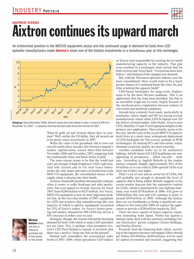
While the value of the greenback slid to lows not seen for nearly three decades, the German company’s market capitalization soared three-fold between November 2006 and November 2007, outpacing both the traditionally shiny and black forms of gold.
The main reason seems to be that the world just can’t get enough of high-brightness LEDs right now. And with Aixtron and its US rival Veeco Instru-ments the only major providers of production-scale MOCVD equipment, the consolidated nature of the supply chain is playing into their hands.
Aixtron, financially prudent and naturally cautious when it comes to order bookings and sales predic-tions, has even upped its revenue forecast for fiscal 2007 from 8200 million to 8215 million. For Veeco, MOCVD equipment is now its most important prod-uct line. In the first nine months of 2007, equipment for LED and wireless chip manufacturing (the vast majority of which is epitaxy equipment) accounted for 35% of Veeco’s orders. As Veeco’s fastest grow-ing end market, demand for HB-LEDs has driven a 45% increase in orders year on year.
Strangely, though, the reasons behind the booming demand for tools with which to make LED epiwafers are not clear. This is perhaps what prompted Aix-tron’s CEO Paul Hyland to remark to investors that there was a need to “keep our feet on the ground”.
Hyland well remembers the unsustained order boom of 2003–2004, where speculative LED makers
in Taiwan were responsible for creating far too much manufacturing capacity in the industry. That glut soon resulted in a prolonged slack period that hit both Aixtron and Veeco hard. “Aixtron has been here before,” said Hyland of the rampant tool demand.
But, with the Taiwanese epiwafer industry now far more consolidated, there would seem to be a much greater chance of a sustained boom this time. So, just what is behind the capacity build?
LED-based backlights for large-scale displays seem to be the most obvious candidate. This is an application that has long been heralded, but that is an incredibly tough one to crack, largely because of the cut-throat price competition between makers of televisions and notebook computers.
Inroads have certainly been made, particularly in notebooks, where Apple and HP are among several manufacturers whose white LED-lit laptops now fill the shelves of retail outlets. John Peeler, Veeco’s new CEO, identifies 13 and 15 inch laptop backlights as the primary new application. That certainly seems to be the case, but the scale of the recent MOCVD capacity build hints at a much more widespread deployment of LED backlights for flat screens, perhaps in RGB technologies for desktop PCs and televisions, where demands on picture quality are more exacting.
Another candidate looks set to be automotive lighting. InGaN-based full LED headlamps are now appearing in production – albeit top-end – Audi cars. According to Jagdish Rebello at the market analyst company iSuppli, approximately 30% of the 65 million or so cars sold in 2006 sported LEDs in at least one of their rear lights.
That’s a lot of cars and an awful lot of LEDs, but still probably not enough to demand the level of capacity that is being added. Rebello suggests in his recent market forecast that the automotive market for LEDs, which is dominated by rear lighting func-tions, was worth $378 million in 2006, will grow to $450 million this year and will continue to grow to around $550 million in 2008. Although the analyst does not see headlamps as being a significant con-tributor to this total until 2009, he expects the appli-cation to provide a $200 million market by 2012.
There are more signals of future capacity expan-sion emanating from Japan. Nichia has agreed a mutual equity deal with key partners including Citi-zen Electronics’ parent company Citizen Holdings, and Stanley Electric.
Proceeds from the financing deal, which, accord-ing to the Japanese business newspaper Nikkei should net Nichia ¥29.4 billion ($269 million), will be used for capital investment and research, suggesting that
Aixtron continues its upward marchAn entrenched position in the MOCVD equipment sector and the continued surge in demand for tools from LED epiwafer manufacturers made Aixtron’s stock one of the hottest investments in a tumultuous year on the exchanges.
E q u i p m E n t V E n d o r s
Nov 06
Dec 06
Jan 07
Feb 0
7
Mar 07
Apr 0
7
May 07
Jun 07
Jul 07
Aug 0
7
Sep 0
7Oct
07
Nov 07
date
10
9
8
7
6
5
4
3
2
7
Going up: Since November 2006, Aixtron’s share price has tripled in value. It stood at 79.4 on November 12, 2007 – a valuation that has not been seen since the summer of 2002.
Michael Hatcher does not own or intend to purchase any of the stocks in this article.
YAh
OO
FIN
ANC
E
CSDec07Portfolio.indd 12 20/11/07 14:33:34

Compound Semiconductor December 2007 compoundsemiconductor.net 13
Indus t r y P o r t f o l i o
Project2 10/9/07 09:44 Page 1
another capacity build is on the cards.Since Citizen Electronics pioneered the develop-
ment of LED backlights for small LCD screens in mobile handsets, it is reasonable to speculate that the firm is now looking towards larger screens as returns from the handset sector continue to diminish.
Stanley’s key focus has typically been on lighting products for the automotive industry. This suggests that the white LEDs of which Nichia has long been the dominant global supplier will now break through into the headlamp function.
Citizen is also branching out of the backlight sector and moving into general illumination. It is already shipping samples of a 540 lm, 74 lm/W LED lamp as an alternative to traditional 40 W light bulbs (40 W bulbs deliver 485 lm at an efficacy of only 12 lm/W), and it is ramping this product for mass-production starting in January 2008.
“We are convinced that this product, which can provide luminous flux on a par with widely used general lighting, will open up new possibilities in the development of lighting applications,” commented Citizen. If the company is anywhere near as suc-cessful in this venture as it has been with its handset backlights, it is going to need a hell of a lot of power LED chips from Nichia.
So it seems that the demand for MOCVD equip-ment is not coming from the sudden adoption of LEDs in a single new application area. Rather, there is robust demand across the whole board – laptop screens, cars, camera flash units in phone handsets, and general illumination. That sounds like good news for Veeco and Aixtron as they move into what is already shaping up to be another very strong year for sales of MOCVD equipment.
Binned and tested at a drive current of 1 A, the new Luxeon K2 LED from Philips Lumileds is based on the company’s thin-film flip-chip technology. Demand for high-performance LEDs like these is behind a sharp uptick in MOCVD equipment orders.
PhiL
iPS
LuM
iLED
S
CSDec07Portfolio.indd 13 20/11/07 14:33:53

compoundsemiconductor.net December 2007 Compound Semiconductor14
Technology W a f e r P r o c e s s i n g
Six Sigma analysis has driven substantial cuts in Skyworks’ photoresist consumption and has resulted in annual savings in excess of $450,000, according to Jens Riege.
Photoresist cuts strengthen Skyworks’ gross marginNobody wants to waste 99% of the expensive materials that they use in highvolume production processes. But that is what happens when semiconductor manufacturers coat their wafers with photoresists. During the spincoating process a large proportion of the resist is flung off or lost through evaporation and less than onehundredth of the original volume used forms a film on the wafer.
This wastage is highly undesirable because typical photoresists cost hundreds of dollars per liter and they are used for multiple spincoating processes during device manufacture. Annual expenditure on these types of material can run into hundreds of thousands of dollars, so reducing their consumption can bring significant cost savings.
At Skyworks Solutions’ Newbury Park GaAs wafer fab in California, we have tried to do this by running a Six Sigma project to cut our photoresist bill. This effort focused on reducing the cost and waste of our photoresist coating step without impacting our products or downstream processes. We restricted our study to the two highestvolume resists, which saved time but allowed the project to make a big impact. That’s because these two solutions account for 80% of all of our resist costs and more than 2% of our total wafermanufacturing costs.
The photoresists are applied to the wafer during photolithography processes using a dedicated tool with a nozzle. Before we started the project we routinely used 2.1 ml/wafer of photoresist. We decided to reduce this resist dispense volume in two phases. Initially we cut our photoresist to 1.5 ml to make cost savings. Then we evaluated further reductions.
The Six Sigma approachEvery Six Sigma project begins with the writing of a project charter. In our case, this document set out the project’s objective, scope and schedule, with the business case, constraints, assumptions and estimated cost savings. Internal customers from the wet etch, dry etch and photolithography process groups were invited to join our team, which allowed us to listen to their concerns and incorporate their needs into the process. This team identified the common variables that could affect the resist coat process in a fishbone diagram (figure 1). Once the management had approved the project’s definition and outline in a tollgate review, we moved on to the measure stage.
This part of the project focused on compiling base
line data for future comparisons, which were gathered from daily resist thickness and crosssection measurements for both standard and imagereverse resist processes. The data’s units, equipment settings and stepbystep measurement methodologies were reviewed by our team and the relevant operators. The fishbone diagram created in the first stage of the project was used to identify the variables that were expected to have the largest impact on resist uniformity control.
We also carried out an informal survey at CS Mantech 2006 to see how our resist dispense vol
manpower material
temperaturephotospeed
temperaturesurface
conditiontopographymaterial
wafer
dispense volume
solids contentthicknessviscosity
batch
variation
resist
exha
ust
temp.
humidi
ty
strok
e len
gthve
locity
accu
racy
repea
tabil
ity
tempe
ratu
re
exha
ust
time
flow
pres
sure
unifo
rmity
disp
ense
noz
zlere
sist p
ump
spin
mot
or
fab
air pr
essu
retem
p.
humidi
ty
environment measurement
ellipsometer
CD SEM
FIB SEM
temperature repeatability
accuracyspin speed at dispense
HMDS
chuc
k
disp
ense
cup
hotp
late
back
side r
inse
suckback
method
machine
position
machine to machine variation
coat wafer withphotoresist
equipmenttechnician
engineeringtechnician
operator
dynamic staticnozzle position
dispense time
dispense rate
stamicautomated
dry timedry spin time
coat recipe
Sk
ywo
rk
S
CSDec07Skyworks.indd 14 20/11/07 14:16:58

Compound Semiconductor December 2007 compoundsemiconductor.net 15
Technology W a f e r P r o c e s s i n g
Photoresist cuts strengthen Skyworks’ gross margin
ume compared with that of five other GaAs manu-facturers (figure 2, p16). These results highlighted the large differences in the photoresist volumes used and indicated that it might be possible to reduce the resist dispense to 0.7 ml per wafer.
We constrained our investigations to resist thick-nesses of between 1.25 and 3.0 μm. To find the dis-pense volume lower limit for this range, we coated 25 wafers with various dispense volumes, which varied from the 2.1 ml/wafer used historically, to just 0.5 ml/wafer (figures 3 and 4, p16). Analysis revealed that a dispense volume of 0.7 ml gives
acceptable and repeatable resist uniformity. Cross-sectional images of transistors coated with this amount of material revealed a 1.25 μm thick resist with a coverage quality comparable to all other resist dispense volumes. A 0.5 ml dispense volume can still produce good resist coverage, but this film does not always coat all of the wafers completely.
The 0.7 ml dispense volume produced a coating that is stable over short periods of time. However, any equipment or process drift towards smaller dis-pense volumes could jeopardize this stability, so we selected 1.0 ml/wafer as our target for resist reduction.
Many wafer fabs can experience process problems that are not solved fully after the first attempt. Altering one particular variable that is not considered critical, and may be related to the material, process, equipment or the environment, can cause problems by making the overall production process unstable. If a problem-solving team cannot quickly identify what has gone wrong, this problem can escalate and cause havoc within a semiconductor company.
Tough problems can be solved by forming a “tiger team” that performs a brainstorming exercise to identify the most likely causes. The team can then run a series of short experiments, implement the most promising solution and hopefully solve the problem.
A more thorough team could run a machine/process capability study. Experiments are used to identify the key variables and ensure that controls are in place to keep the processes and equipment stable. Techniques such as the “8-discipline” approach can also be used, which involve asking questions to get to the root of a problem and finding ways to make sure that the problem does not happen again.
The Six Sigma methodology draws on all of these problem-solving approaches, but in a manner that guides the team to a permanent, sustainable solution. Data, rather than gut feeling, drive every team
decision. But, more important, Six Sigma considers the expectations of internal and external customers to ensure a successful outcome.
This approach is not suitable for all projects, but it is applicable to stubborn, challenging or customer-driven problems that cannot be solved easily by other applicable methods.
Projects consist of five stages. Progress to the next stage hinges on a successful tollgate review with the management. These reviews ensure that the project is still receiving management support and meeting its agreed objectives. The five stages are defined below.● The define stage determines the external and internal customer expectations of the outcome of a successful project. A project charter is drawn up to define the project, team members, project goal, benefits, assumptions, constraints, project scope and preliminary timeline. Common tools for this stage include brainstorming and Pareto analysis.● The measure stage identifies all existing process data required to form a reference baseline. Any implemented process changes have to show an improvement relative to this baseline. Data-collection methods also have to be agreed and documented to ensure consistency between operators. Typical
tools used for this stage, which requires team members to agree on the direction and focus of the project, include “operational definitions” and “cause and effect” (fishbone) diagrams.● The analyze stage examines any variations in baseline data and searches for a pattern. Experiments are conducted to reveal the most critical variables in achieving success. Settings for the variables that produce the best and most stable process conditions are analyzed and confirmed in sample test runs. The common tools for this stage of work are designed experiments and statistical data analysis.● The improve stage involves employing the most successful test results in the trials. Statistical data analysis of the pilot data determines whether the process change meets the requirements for full production. These requirements relate to effectiveness, the project’s definition and safety. “Failure modes” tools and statistical data analysis are often used here.● The control stage, which is often neglected by other problem-solving methods, determines whether any process changes cause critical characteristics to become unstable over time. Tools for these assessments include control charts and process capability indices, which must be evaluated at regular and frequent time intervals.
Why bother with Six Sigma?
manpower material
temperaturephotospeed
temperaturesurface
conditiontopographymaterial
wafer
dispense volume
solids contentthicknessviscosity
batch
variation
resist
exha
ust
temp.
humidi
ty
strok
e len
gthve
locity
accu
racy
repea
tabil
ity
tempe
ratu
re
exha
ust
time
flow
pres
sure
unifo
rmity
disp
ense
noz
zlere
sist p
ump
spin
mot
or
fab
air pr
essu
retem
p.
humidi
ty
environment measurement
ellipsometer
CD SEM
FIB SEM
temperature repeatability
accuracyspin speed at dispense
HMDS
chuc
k
disp
ense
cup
hotp
late
back
side r
inse
suckback
method
machine
position
machine to machine variation
coat wafer withphotoresist
equipmenttechnician
engineeringtechnician
operator
dynamic staticnozzle position
dispense time
dispense rate
stamicautomated
dry timedry spin time
coat recipe
Fig. 1. (left) Skyworks’ fishbone diagram displays the critical process output variable as the head of a fish. The spines of the fish – man, method, machine, material, measurement and environment – list all of the various process characteristics that can affect this output variable.
CSDec07Skyworks.indd 15 20/11/07 14:17:29

compoundsemiconductor.net December 2007 Compound Semiconductor16
Technology W a f e r P r o c e s s i n g
After completing a successful tollgate review for this section of the project, we went on to analyze which process variables could be adjusted to produce the largest gains for meeting our overall goals.
For the analyze stage we carried out further experiments at a variety of resist dispense volumes and determined the impact that these changes had on our critical process characteristics. Measurements of the developed resist’s profile, linewidth crosssection and electrical characteristics were made. If any particular set of process conditions produced values inferior to those associated with the standard process, then those conditions were discarded.
We also analyzed the resist temperature, dispense nozzle position and whether the wafer was spinning as the photoresist was dispensed, to judge their effects on resist thickness uniformity. Statistical ttests revealed that thickness uniformity was not affected by temperature or nozzle position, while dispensing the photoresist on a spinning wafer brought slight improvements over the static equivalent. Meanwhile, images of the standard and liftoff resist profiles revealed that the resist’s coverage quality was not diminished by wafers with a more rugged topography. These and other results indicated that it made sense to test a 1.0 ml/wafer dispense volume in mainstream production.
In the fourth stage, we used photoresist films with a 1.0 ml dispense volume on a limited number of production wafers. We processed three production lots, treating half of the wafers with 1.0 ml dispense volumes and the other half with the standard 1.5 ml. For each of these lots, the critical dimensions of the wafer were measured at each coatprocessing step using a scanning electron microscope.
No statistical difference was found between the thickness of the majority of process layers produced by both methods and any differences were within the measurement error of the imaging tool. Most of the electrical data from the wafers with the lower dispense volume told a similar story. In the cases where differences did occur, these were within the fluctuations associated with the standard process,
according to historical production lot data.Although our new process gave the same results as
our existing one, we could not ignore our customer’s concerns. So we asked them to help us to complete a failure mode and effects analysis (FMEA) study – a systematic review of potential process failures that can determine possible causes for each failure. For each cause, the team suggested some controls that could prevent failure.
This team also identified causes of failure that occur frequently or have a small chance of detection or prevention, and defined and implemented actions that address each of these concerns. The processcontrol plan was also updated to ensure that equipment and process controls were in place for each critical processcontrol characteristic. Finally, we released the process change on one of our coater tracks as part of a pilot production ramp.
We then entered the control phase, which required a review of the first month’s production data. No process shifts were observed and we confidently released the process on our remaining coat tracks. One month’s data from all of these tracks and electrical test data revealed no process shift.
These results left one hurdle to full production release – verification that outofcontrol action plans were in place for all known process failures. These would direct production technicians to the appropriate response procedure, should the process fail. Action plans were put in place by storing the project data in a central repository, which was referenced by a storyboard that included links to all data, reports, actions taken and improvements made.
Our first year of production with the new process has validated the success of the Six Sigma project. After cutting the photoresist dispense volume from 2.1 to 1.0 ml/wafer, critical wafer dimensions have remained stable, our downstream process has not shifted and the reduced material consumption (confirmed independently by the Skyworks Environmental Department) has saved our company nearly $0.5 million. We have also had no complaints downstream or from external customers.
About the authorJens Riege ([email protected]) is an ASQ Certified Six Sigma Black Belt and principal engineer at Skyworks Solutions in Newbury Park, California. He helped to implement Six Sigma within Skyworks and works on projects in the photolithography, implant, plating, thin-film and final processing areas.
0.030
0.025
0.020
0.015
0.010
0.005
0.000B (4") C (6") F (4") E (6") SKY (4") D (6")
GaAs wafer fab (wafer size)
disp
ense
vol
ume
(ml/
wafe
r cm
2 )
phase 1
phase 2
Fig. 2. (left) A survey at CS Mantech 2006, which was held in Vancouver, Canada, revealed the large variation in resist dispense volumes between several GaAs chip manufacturers. Skyworks’ Newbury Park facility (SKY) used a relatively large volume of resist before the Six Sigma project, which lowered this value in two phases. The data are normalized to dispense volume/wafer surface area. None of the sites used a solvent pre-wet before resist dispense. Fig. 3. (above) Trials for dispense volumes ranging from 0.5 to 2.1 ml showed that good coverage is possible in all cases. However, it was found that a volume of 0.5 ml doesn’t always coat the wafers completely.
1.0 ml
1.5 ml
� l
1 µm
2.1 ml 1.5 ml 1.2 ml
1.0 ml 0.7 ml 0.5 ml
5 µm
Fig. 4. Cross-sectional images of wafers coated with a 2.5 µm thick lift-off resist show the acceptability of 1.5 and 1.0 ml resist coatings.
CSDec07Skyworks.indd 16 20/11/07 14:18:06

Compound Semiconductor December 2007 compoundsemiconductor.net 17
Technology C o n f e r e n C e r e p o r t
SiC readies itself to save the worldBut can the industry’s businesses save themselves as they compete with each other in a tight niche for limited sales to final consumers? Andy Extance was in Otsu, Japan, to document the aspirations and growing pains, as well as the latest research on show in this maturing field at ICSCRM 2007.
Al Gore and the International Panel on Climate Change were named the winners of the Nobel Peace Prize while I was on the way to Otsu, Japan, to attend the 2007 International Conference on Silicon Carbide and Related Materials. This fact was not lost on the participants in the plenary session of the ICSCRM conference, affectionately termed “ice cream”. On the first morning, representatives of SiCED and Toyota mentioned this piece of news in the same breath as the potential efficiency benefits of replacing silicon with SiC. When describing the energy savings arising from using SiC devices as industrial inverters, SiCED’s Dethard Peters commented: “The world is waiting for solutions to global warming and we have silicon carbide in our hands.”
Addressing the crowd at the conference banquet, the governor of Shiga prefecture, of which Otsu is the capital, picked up the theme. With a background as an academic ecologist and having jurisdiction over Lake Biwa, the world heritage site onto which the conference backed, she was proud to be associated with a potentially “environmentally friendly” technology.
Such a reputation will hardly do the SiC community any harm, but perhaps it is a little early to be trying to get associated with Gore et al. “We thought we had enough to do getting defect levels down and making devices, and now we have to save the world?” was one anonymously reported response to the green tinge that shaded the conference.
Back in the plenary session, Kimori Hamada of Toyota emphasized that his company anticipated using SiC in its hybrid cars at some point in the
2010s. However, his requirements for SiC demand high performance at a cost to match silicon.
SiCED’s Peters almost immediately delivered on that requirement, asserting in his plenary talk that the Schottky diodes that it has helped Infineon to develop are economically competitive with silicon today. Enjoying a privileged position in German industry (owned by Siemens and collaborating with Infineon), SiCED is looking to develop JFETs and MOSFETs rapidly to join Infineon’s Schottky diodes.
Regardless of these commercial promises, many of the conference participants were nervous about the industry’s prospects, not least the representatives of the growing number of SiC wafer suppliers. While Cree remained the mostmentioned provider in the talks, SiXON – a well reputed Japanese wafer supplier – announced its closure. In SiXON’s place, two new SiC firms made their debut: Crysband of South Korea and TanKeBlue of China.
Cree – keeping ahead of the packIn the remaining plenary talk, Cree’s Al Burk went over the history of SiC growth, leading up to his firm’s current leadership in the substrate market with its 4 inch (100 mm in Cree’s terminology) zeromicropipe wafers. Burk focused on the predecessors who made Cree’s current position possible, before rushing through the design details of the 8 × 100 mm wafer warmwall planetary SiCVPE reactors in use at the company. Burk’s colleague Joe Sumakeris explained the elegant way in which Cree can improve the thickness and doping uniformity
The International Conference on Silicon Carbide and Related Materials (ICSCRM) 2007 was held at the Otsu Prince Hotel in Otsu, Japan, on 14–19 October. 43 exhibitors and 604 delegates gathered from 26 countries to attend and enjoy the surroundings of Lake Biwa, the largest lake in Japan and one of the world’s four most ancient lakes.
ICS
CR
M 20
07
CSDec07ConferenceReport.indd 17 20/11/07 14:20:58

compoundsemiconductor.net December 2007 Compound Semiconductor18
Technology C o n f e r e n C e r e p o r t
of its 100 mm wafers, using horizontal flow rather than planetary reactors. Introducing additional pro-pane to the chamber through a secondary carbon source channel helps to reduce the thickening and increased doping seen at the wafer edges. Adding supplementary hydrogen stops graphite precipita-tion in the reactor and the undesirable defects that this causes in the growing wafers.
Having nailed down zero-micropipe growth on the 4 inch scale, Cree is now lowering “1c-screw” dis-location density. Robert Leonard presented detailed wafer mapping to show that process developments at Cree have more than halved the number of 1c-screw dislocations. Standard processes gave 1c densities of 850 cm–2, but Leonard showed improved median densities of 325 cm–2 that went as low as 175 cm–2 on 3 inch 4H SiC wafers. Cutting 1c-screw dislocation density lowers the leakage current of devices grown on SiC substrates, according to Leonard.
A good chunk of research presented at ICSCRM was focused on developing ways to improve crystal quality that avoid Cree’s strong intellectual property position. For example, Cree has patented the KOH etching of wafers to reduce the density of basal plane dislocations (BPDs). These cause stacking plane faults that degrade the performance of certain SiC devices when a current is applied, so an alternative method coming out of the US Naval Research Labor-atory in Washington attracted a lot of interest. In a single step of what he called an interrupted growth method, Robert Stahlbush was able to convert 30% of a wafer’s BPDs to less problematic threading etch dislocations (TEDs). This can then be repeated to diminish BPD levels further. While remaining wary of releasing precise details of the process, Stahlbush explained that the discovery was made while study-ing BPD evolution during epitaxial growth. During these studies, some BPDs would turn to TEDs at the beginning of each epitaxial run.
How quickly can SiC grow?With end users like Toyota putting price-for- performance at the top of their SiC wish list, the High Growth Rate session drew a lot of attention. The key to the achievement of high growth rates is suppressing nucleation in the gases used in the reac-tors. The session split in two, between European researchers who use different types of chlorine-based chemicals to suppress nucleation, and Japan-ese researchers who focus on gas control.
In chlorine chemistry, US start-up Caracal and Linköping University attained 4H SiC growth rates of higher than 100 μm/h by using methyltrichloro-silane as a growth precursor. The same collaboration achieved on-axis crystal growth that produced 100% of the 4H SiC polytype at 20 μm/h. On-axis growth is difficult because it can lead to a SiC crystal com-posed of a mixture of polytypes, but it is desirable because it will eliminate the BPD problem.
By contrast, researchers from Japan’s Center of Research for the Electrical Power Industry attained
a 135 μm/h growth rate using a more conventional gas mixture. The key to stopping nucleation in hydrogen/silane/propane is growing your crystal at 40 Torr pressure, according to Masahiko Ito. A sim-ilar low-pressure method at 20 Torr, with a greater focus on reactor design, scored a growth rate of 140 μm/h for Yuuki Ishida of Japan’s Advanced Institute for Science and Technology.
Toyota was not the only Japanese conglomer-ate present. Among the device-related papers, big hitters like Toshiba, Panasonic, Mitsubishi, Hitachi, Nissan and representatives from Japanese electrical power companies stepped up to show their form in the SiC arena. Amid a plethora of devices, a strong body of MOSFET research came through to show SiCED and its collaborators that they will not have the SiC MOSFET field to themselves. Many groups focused their attention on the problem of the trap-ping of electrons between SiC and any potential gate oxide without producing commercial devices.
While we wait for the full range of SiC devices to work through to commercialization, the next to market could result from military contracts. Victor Veliadis of Northrop Grumman presented a 0.1 cm2 vertical JFET that has attained breakdown voltages of more than 1980 V for the US Army. David Spry from NASA showed how the SiC VJFETs that he is devel-oping for sensing applications can operate stably at over 500 ºC for 2000 h, with tests still ongoing.
So, although there was much in Otsu to be pos-itive about, it is clear that the SiC community faces a myriad of challenges before it can meet its full potential. In the meantime there are a lot of people performing work with a limited amount of cash from sales to end consumers flowing into the industry.
Specialist power electronics consultancy Yole Développement has estimated that SiC device sales in the power sector came to $15 million for 2006, split evenly between Infineon and Cree.
On the Thursday of the conference week, Cree announced that its total sales for the preceding quarter had hit $113 million – $8.5 million of this revenue was derived from materials, and power devices brought in just $4 million. Just as Cree is a big fish in the small SiC pond, so the kind of appli-cations that were discussed at ICSCRM are cur-rently of secondary financial importance at Cree.
The upside to this is that industry giants continue to line up behind SiC, lending weight to Yole’s claims that the annual device market will be worth $800 million by 2015. After Cree’s results were announced, its Otsu contingent gathered for a cel-ebration, confident that they will be around to reap the benefits of the industry’s expansion. Many other companies may be equally confident, but SiXON has showed how the competition between SiC wafer makers is getting tougher. Perhaps, in such a tightly balanced business, the motivation for each individ-ual company to make breakthroughs and stay ahead of its competitors will help to kick off the SiC device growth ramp sooner than anticipated.
Kimimori Hamada (above) of Toyota told the conference that SiC will have a part to play in his company’s hybrid technology before 2020, as it strives to produce the “ultimate ecovehicle”. The Otsu Prince Hotel (below) was host to an audience of which Japanese participants made up 57%.
ICS
CR
M 2
007
A Ex
TAn
CE
� l
CSDec07ConferenceReport.indd 18 20/11/07 14:21:24

?gatan gets it
*Results courtesy of Dr. Uwe Jahn of the Paul Drude Institute for Solid State Electronics, Berlin, who used these results to understand the relationship between the metal organic chemical vapor deposition parameters and the material quality for (Al,Ga)N layers grown on sapphire. Composite image derived from 4 monochromatic CL images plus SE image.
1µm T=6K
Defect distribution and compositional
variations in a light-emitting
material revealed by CL imaging and spectrum imaging
Does your spectroscopy system
give you the full picture when studying
opto-electronicmaterials?
To learn how our cathodoluminescence
(CL) products accomplish this,
visit us at www.gatan.com/answers
MonoCL3+,XiCLone,
liquid heliumSEM stage
Untitled-1 1 16/11/07 10:16:52

Compound Semiconductor December 2007 compoundsemiconductor.net20
PMGI/LOR Resists for Lift-off ProcessingMicroChem CorpPMGI and LOR resists allow exceptionally good deposition control whenused as an undercut layer in bi-layer lift-off processing. PMGI resists areideally suited for high resolution (sub 0.25 µm) lift-off processes, whileLOR resists are better suited for thick >1 um) metal deposition processes.Both products permit easy process tuning, high yields, superior deposition
line width control and are easily stripped. PMGIand LOR resists are compatible and won’tintermix with conventional DUV, i-line and e-beam resists. Mainstream lift-off applicationsinclude GMR & MR heads, wireless devices,opto-electronics, sensors, MEMs, and advancedIC packaging. These products are also wellsuited as sacrificial layers for applications suchas air bridges.
Contact Sales at MicroChem, 1254 Chestnut St.
Newton, MA02464, USA
Tel +1 617 965 5511 Fax +1 617 965 5818
Web www.microchem.com
PRODUCT SHOWCASE / CLASS I F I EDCOMPANYBULLETINBANNER
Promote your company message, products and jobs with this banner for only £500 perissue. Contact David Iddon on +44 117 930 1032, e-mail: [email protected] orRosemarie Guardino on +1 215 627 0880, e-mail: [email protected]
Our client is a European based Nanotechnology start-up with focus onthe research, development and commercialisation of III-V quantumnanowire devices for the semiconductor markets. Differentiating itselffrom that of other “Nano-tech” companies, their process actually canbe characterised as being sub-nano involving atomic layer control ofthe semiconducting structures.Targeting electronics, optoelectronics and sensor markets and boast-ing an engineering team of industry recognised figureheads and acommercially experienced management team, our client estimates itstotal addressable market to be in excess of $40BN. Having received significant funding, our client is seeking the followingtwo key recruits to drive R&D and transfer products through volumeproduction into commercialisation.
PRODUCT DEVELOPMENT MANAGER Ref: CS1103Lead a growing product development team, managing the develop-ment of optoelectronic devices based on proprietary processing tech-nology. Ideal candidates will have experience of:
• Product development – semiconductor devices, ideally opto-electronics
• Product qualification, planning and defining process and goalsfor development
• Release to manufacturing
PROCESSING & GROWTH MANAGER Ref: CS1102You will be responsible for a laboratory based team using MOCVD forIII-V nanowire growth as well as other processing techniques. Keyresponsibilities include:
• Manage MOCVD growth and wafer processes• Support product development of optoelectronic devices • Establish working processes and help optimise the workflow
To apply and receive more information send your CV [email protected]
or call Daniel Reddyhough on 01344 360100.
FibreSystems Europe isthe leading voice and
champion of the opticalcommunications
industry in Europe
Published every other month, each issuedelivers coverage of:
• applications, R&D, business and patentsnews
• feature articles covering all aspects of theindustry
• opinion and analysis on the latest researchand technologies
• company profiles and interviews with key industry personalities
• new products
Free subscriptions are available atwww.fibresystems.org/subscribe.
CSDecProdShowcase 20/11/07 11:26 Page 27

Compound Semiconductor December 2007 compoundsemiconductor.net 21
Technology G a a s T r a n s i s T o r s
At TriQuint Semiconductor we are planning to join a handful of manufacturers offering high- functionality integrated chips with the launch of a BiHEMT manufacturing process in the second half of 2008. This technology, which unites power HBTs and E/D PHEMTs, will target existing applications that have previously required hybrid HBT/PHEMT approaches and new applications that will also bene-fit from this form of monolithic integration.
Our technology will enable the integration of high-efficiency HBT power amplifiers (PAs) with E/D PHEMT-based logic and control circuitry, low-noise amplifiers (LNAs), and bypass, bias and antenna switches. It will also deliver other benefits, such as HBT-based electrostatic damage-protection circuitry, which is more effective and compact than similar schemes employing PHEMTs.
Recently, other GaAs manufacturers have devel-oped monolithic chips incorporating FETs and HBTs. These chips have improved bias control cir-cuitry and bypass switches in cellphone PAs, and have even found application as integrated LNAs and PAs for WLAN. But it is possible to raise PHEMT performance to a level suitable for power switch applications, which allows PAs and antenna switches to be integrated onto a single chip.
Our BiHEMT process promises exactly that. Although the GaAs cost per unit area is higher than that for standalone HBT or PHEMT fabrication, our approach promises cheaper and smaller modules because it eliminates the bondpads and bondwires used to connect the different types of transistor.
While it delivers many advantages, the BiHEMT approach is not suitable for all applications. Not all future power modules will need this technol-ogy. Those modules where a hybrid system based on a separate HBT and PHEMT-based die is cheaper will not use our approach. But our tech-nology, and other schemes for integrating HBTs and FETs, will be cost competitive for today’s W-CDMA applications and next-generation highly integrated radio front-ends.
Like most GaAs HBT/FET integration technol-ogies, our approach is an extension of an exist-ing HBT process, with PHEMT-specific steps inserted between HBT device-specific processes and passive/interconnect metallization formation. Our PHEMT’s high performance is ensured by separating this device from the HBT with an etch-stop layer (figure 1, p22). This design philosophy means that the entire AlGaAs/InGaAs PHEMT
epitaxial stack – including the heavily doped GaAs ohmic contact layer – is placed under the GaAs/GaInP HBT subcollector. The PHEMT is electric-ally isolated from parasitic capacitances because it sits directly on the semi-insulating GaAs sub-strate. Consequently there are no compromises in the PHEMT epitaxial structure that require special
TriQuint Semiconductor has united its HBTs and PHEMTs with a BiHEMT process that promises to integrate power amplifiers and antenna switches on the same chip, according to Tim Henderson.
TriQuint joins the integration game
150 mm GaAs wafers being prepared for a gold-plating bath in TriQuint’s Oregon fab. The company is addressing the demand for smaller devices with greater functionality with a BiHEMT process that combines HBTs and PHEMTs on one chip. This promises to unite power amplifiers with logic and bias control circuitry, low-noise amplifiers and ultimately antenna switches.
TriQ
uin
T
CSDec07Triquint.indd 21 20/11/07 14:14:50
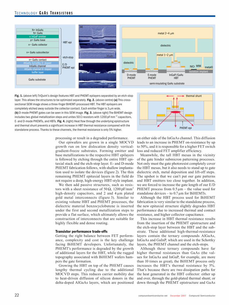
compoundsemiconductor.net December 2007 Compound Semiconductor22
Technology G a a s T r a n s i s T o r s
processing or result in a degraded performance.Our epiwafers are grown in a single MOCVD
growth run on low dislocation density vertical- gradient-freeze substrates. Forming emitter and base metallizations to the respective HBT epilayers is followed by etching through the entire HBT epi-taxial stack and the etch-stop layer. E- and D-mode PHEMT fabrication follows, with shallow implanta-tion used to isolate the devices (figure 2). The thin remaining PHEMT epitaxial layers in the field do not require a deep, high-energy HBT-style implant.
We then add passive structures, such as resis-tors with a sheet resistance of 50 Ω, 1200 pF/mm2 high-density capacitors, and 2 and 4 µm plated gold metal interconnects (figure 3). Similar to existing volume HBT and PHEMT processes, the dielectric material benzocyclobutene is inserted under the first and second metallization steps to provide a flat surface, which ultimately allows the construction of interconnects that are suitable for highly flexible and dense routing.
Transistor performance trade-offsGetting the right balance between FET perform-ance, complexity and cost is the key challenge facing BiHEMT developers. Unfortunately, the PHEMT’s performance is degraded by the growth of additional layers for the HBT, while the rugged topography associated with BiHEMT wafers ham-pers the gate formation.
Growing the HBT on top of the PHEMT causes lengthy thermal cycling due to the additional MOCVD steps. This reduces carrier mobility due to heat-driven diffusion of silicon donors in the delta-doped AlGaAs layers, which are positioned
on either side of the InGaAs channel. This diffusion leads to an increase in PHEMT on-resistance by up to 50%, and it is responsible for a higher FET switch loss and reduced FET amplifier efficiency.
Meanwhile, the tall HBT mesas in the vicinity of the gate hinder submicron patterning processes. Not only must the gate photoresist completely cover the HBT mesas, but it also needs to stand up to gate dielectric etch, metal deposition and lift-off steps. The upshot is that we can’t put our gate patterns and HBT emitters too close together. In addition, we are forced to increase the gate length of our E/D PHEMT process from 0.5 µm – the value used for standalone devices – to 0.7 µm for BiHEMTs.
Although the HBT process used for BiHEMT fabrication is very similar to the standalone process, the new epitaxial structure slightly degrades HBT performance due to increased thermal and contact resistance, and higher collector capacitance.
This increase in HBT thermal resistance results from the insertion of the PHEMT epistructure and the etch-stop layer between the HBT and the sub-strate. These additional high-thermal-resistance layers contain the ternary compounds AlGaAs, InGaAs and GaInP, which are used in the Schottky layers, the PHEMT channel and the etch-stops.
Although these ternary compounds have far higher thermal resistances than GaAs (the val-ues for InGaAs and InGaP, for example, are more than 10 times as great), the BiHEMT process only increases the HBT’s thermal resistance by 5%. That’s because there are two dissipation paths for the heat generated in the HBT collector: either up and over, through the gold-plated thermal shunt; or down through the PHEMT epistructure and GaAs
dielectric
metal0
semi-insulating GaAs substrate
dielectric
metal 1–2 µm
metal 2–4 µm
isolation implant
MIMNiCr
InGaP/GaAsHBT
E-modePHEMT
D-modePHEMT
thermal shunt
PHEMT epi
Fig. 1. (above left) TriQuint’s design features HBT and PHEMT epilayers separated by an etch-stop layer. This allows the structures to be optimized separately. Fig. 2. (above centre) (a) This cross-sectional SEM image shows a three-finger BiHEMT-processed HBT. The HBT epilayers are completely etched away outside the collector contact. Each emitter finger is 3 µm wide. (b) D-mode PHEMT gates can be seen in this SEM image. Fig. 3. (above right) The BiHEMT design includes two global metallization steps and unites 50 Ω resistors with 1200 pF mm–2 capacitors, E- and D-mode PHEMTs, and HBTs. Fig. 4. (right) Heat flow through the underlying epistructure and thermal shunt prevents a significant increase in HBT thermal resistance compared with the standalone process. Thanks to these channels, the thermal resistance is only 5% higher.
1 µm
10 µm
(b)
(a)N+ InGaAsN+ GaAs
n InGaP emitterp+ GaAs base
n– GaAs collector
n+ GaAs subcollector
n+ GaAs contactAIGaAs Schottky δ–doped
InGaAs channel
AIGaAs channel δ–dopedbuffer layer
GaAs substrate
HBT epi
E/DPHEMT epi
etch-stop
CSDec07Triquint.indd 22 20/11/07 14:15:44
Compound Semiconductor December 2007 compoundsemiconductor.net 23
Technology G a a s T r a n s i s T o r s
substrate, which leads to significant lateral heat spreading within the HBT (figure 4, p22).
The HBT’s collector resistance is influenced by the subcollector’s thickness. Selecting the appropriate value requires a trade-off between process complex-ity and subcollector sheet resistance. Contact and undepleted collector resistances also affect the HBT’s collector resistance. The BiHEMT process only leads to a 20% increase in this resistance, despite a three-fold increase in subcollector sheet resistivity.
The BiHEMT process also increases collector capacitance by 10%, due to looser device layout rules that are required for the deep HBT isolation etch.
For HBTs produced by the BiHEMT process, DC and RF device characteristics are essen-tially the same as those for our standalone HBTs, thanks to the similarity of the two processes. For a 3 × (3 × 30) µm2 emitter HBT, the typical current gain is 80, the base-collector breakdown voltage is 24 V, and ft and fmax are 36 and 53 GHz, respect-ively, at 2 V and 20 kA/cm2. ft is unchanged from our standalone HBT process, but fmax suffers from a 10% reduction due to the small increases in the collector’s capacitance and resistance.
Aside from the on-resistance degradation result-ing from subsequent HBT growth, the BiHEMT’s PHEMT performance is similar to that of our nom-inal 0.5 µm E/D PHEMT technology but is scaled by the slightly longer gate. Typical D-mode PHEMTs produce a peak transconductance of 300 mS/mm, a source-drain current of 160 mA/mm and a maxi-mum current of 420 mA/mm. The device’s pinch-off voltage is –0.8 V, its gate-drain breakdown voltage is 22 V and it has an on-resistance of 2.0 Ω-mm. The RF characteristics include a typical ft of 20 GHz and an fmax of 57 GHz.
For an E-mode PHEMT, transconductance hits 460 mS/mm and the current peaks at 240 mA/mm.
This transistor’s typical pinch-off voltage is +0.3 V. It has a gate-drain breakdown voltage of 23 V. The RF characteristics include a typical ft of 22 GHz and an fmax of 65 GHz.
Greater flexibilityOur BiHEMT development will now focus on improving process flexibility. This will allow us to address a larger share of today’s BiHEMT mar-ket, while simultaneously penetrating into new market sectors. Our latest BiHEMTs provide a FET performance suitable only for on-chip con-trol circuitry, bias control and low power switch-ing. However, future applications could include the integration of control circuitry onto the GaAs PA chip, alongside high-power output switches for W-CDMA and ultimately GSM, which would cut module sizes and part count in mobile handsets.
Applications such as this will demand signifi-cant improvements in PHEMT density and per-formance. The goal of integrating GSM PAs and antenna switches on a single chip, for instance, would require a significant improvement in the on- resistance of the PHEMTs in our BiHEMTs to meet the insertion loss goals. Other applications, such as the on-chip integration of high-end transmit and receive parts, will deliver similar improvements in PHEMT technologies. To meet all of these demands will require further innovations in epitaxial growth and process technology.
Further readingT Henderson et al. 2007 CS Mantech Digest 247.C K Lin et al. 2007 CS Mantech Digest 251.W Peatman et al. 2007 CS Mantech Digest 243.R Ramanathan et al. 2007 CS Mantech Digest 255.R Stevenson 2006 Compound Semiconductor September 26.
By Richard StevensonTriQuint, Anadigics, Skyworks Solutions and WIN Semiconductors have developed different technologies to monolithically integrate an HBT with a PHEMT or a FET. TriQuint says that its BiHEMT process is designed to address the needs of internal product designs and foundry customers. As a result, a premium is placed on process flexibility, which means that E- and D-mode gate PHEMT devices are included in the process. (For applications that don’t require both E- and D-mode devices, some process steps can be omitted.)
The key difference between Skyworks and Anadigics, the FET/HBT integrators, is their approach to the FET/HBT epitaxial structure.
Skyworks integrates its MESFET into its HBT emitter structure, which has the benefits of straightforward epitaxial growth
and processing. However, this comes at the expense of FET performance, which is limited by the poor RF isolation of the MESFET.
Anadigics, in contrast, places AlGaAs/InGaAs layers underneath the HBT’s subcollector – a relatively thick layer that doubles as the PHEMT’s heavily doped n-type ohmic contact. This approach produces a PHEMT with good RF isolation at the penalty of a very deep, wide recess and a presumed increase in gate-source spacing, along with a higher drain/source resistance that results from the thick PHEMT contact layer.
TriQuint’s approach differs from that of both Skyworks and Anadigics. The epitaxial layers of the PHEMT and the HBT are completely separated, and there is no compromise in PHEMT epitaxial design, according to the company. Instead, compromises are required
in the actual epitaxy growth; growing an entire HBT structure on top of a PHEMT forces additional thermal cycling compared with a standalone PHEMT. There are also process trade-offs, due to the patterning of submicron gates on wafers with tall HBT mesas.
WIN Semiconductors, a Taiwanese foundry with standalone power HBT and E/D PHEMT processes, has pursued a similar HBT/PHEMT integration approach to TriQuint (see Compound Semiconductor November 2007 p14). The process technology is clearly different but the chips produced also feature E/D-mode PHEMT integration, with the HBT and PHEMT separately optimized. The HBT is grown within the BiHEMT structure and the two types of transistor are completely separated to the extent that they share no epitaxial layers.
Comparing BiFETs and BiHEMTs
About the authorTim Henderson is an engineering fellow in the GaAs process development group based at TriQuint’s Oregon facility. He is responsible for BiHEMT and advanced HBT development.
� l
CSDec07Triquint.indd 23 20/11/07 14:16:16

Signed-up users enjoy unlimited access to premium content.
If you haven’t already done so, sign up for free today!
The essential onlineresource for the physics
community
Visit today to experience brand-
new features:
• daily news and special web-only articles;
• careers and professional-development sections;• a digital edition of Physics World magazine –available for all Institute ofPhysics members;
• a new facility to commenton articles.
M PW AD 0807 Fillers Website-6 23/10/07 09:38 Page 1

Compound Semiconductor December 2007 compoundsemiconductor.net 25
Technology T u n a b l e l a s e r s
Widely tunable lasers are key components in optical networks based on wavelength division multiplexing. They can be used to replace many fixed-wavelength lasers as back-up sources, so long as they can deliver a tuning range in excess of 40 nm and a wavelength switching speed of typically 1 s.
The best designs that meet these requirements use current injection into the semiconductor waveguide to tune the emission wavelength. Since a single-wavelength control region limits tuning to 15 nm, due to the maximum shift in refractive index that can be induced in this type of structure, many of today’s commercial offerings feature filter-based structures.
Such devices, which can cover an entire optical communication band, employ a pair of filters with comb-like reflectivity spectra in differing free spectral ranges (FSRs). Several commercial lasers are based on this technology, including JDSU’s sam-pled grating (SG) DBR laser, Syntune’s Y-branched emitter, and a super-structure-grating distributed Bragg reflector (SSG-DBR) design manufactured by our subsidiary, NTT Electronics Corporation.
Although these lasers can serve today’s optical communication networks, they are not necessarily suitable for next-generation infrastructure, which will be based on optical packet-switching systems. In these systems, wavelength switching will be performed through an arrayed waveguide grating (AWG) filter, with the tunable laser’s wavelengths at the input port dictating the routing/switching of data to the desired output port. For such an approach, rapid switching and tuning of the lasing wavelength is demanded on a packet-by-packet basis.
Tunable lasers operating in this type of network also need to deliver a very stable emission wave-length – even very small frequency drifts can pro-duce cross-talk into the neighboring output ports of the AWG filter. These drifts can occur over rela-tively long time-intervals and are often attributed to variations in injection current during tuning. These variations alter the device’s temperature, leading to changes in refractive index and lasing wavelength.
We have recently invented and demonstrated a widely tunable laser that can fulfill all of these cri-teria (figure 1). This device consists of a gain section, a phase-control region and a double-ring-resonator-connected filter with two micro-ring resonators. The ring resonators are simple circular waveguide structures with several transmission peaks that can
be tuned by varying the injection current. Each of these ring resonators, which are tens of microns in size, are coupled to a straight waveguide via a multi-mode interferometer coupler.
Our micro-ring-based filter is a small, simple structure that reduces overall device costs and increases production yield. In addition, it allows our lasers to be fabricated with the same set of processes that are used to make our other components for a wavelength-routing device. The two steps required to produce DBR-type lasers are also avoided – the regrowth process for burying the gratings and any form of high-resolution lithography.
Our ring resonator has superior spectral charac-teristics compared with SSG and SG lasers, and it features a narrow bandwidth filter with a Lorentzian-
Micro-ring full-band tunable lasers can deliver fast and stable wavelength switching. This makes them the ideal candidate for next-generation networks employing optical packet-switching technology, say Shinji Matsuo and Toru Segawa from NTT Photonics Laboratories, Japan.
Rings speed wavelength switching
–6000 –4000 –2000 0 2000 4000 6000
refle
ctiv
ity
relative optical frequency (GHz)
(b) sampled grating
(a) ring resonator
Fig. 1. (top) (a) Ring resonators are a key part of NTT’s tunable lasers. Injecting current into these structures alters their refractive index, spectral response and ultimately the emission wavelength of the laser. (b) NTT’s 1.55 µm laser chip is just 1.0 × 0.3 mm in size and has a tuning range of more than 50 nm. Fig. 2. (bottom) The ring resonators employed by NTT have a different frequency response from the gratings used by other tunable laser developers. The gratings produce peaks with varying reflectivity that ultimately prevent tunable lasers from providing fast switching, because such structures cannot use low currents to control the emission wavelength. Ring resonators, however, have an infinite number of resonant peaks, which is the key to their fast switching.
10 µm gain section phase ring 1 (FSR1)
ring 2 (FSR2)
(a) (b)
CSDec07NTT.indd 25 20/11/07 14:18:48

compoundsemiconductor.net December 2007 Compound Semiconductor26
Technology T u n a b l e l a s e r s
shaped response and an infinite number of resonant peaks with the same reflectivity (figure 2a, p25). These characteristics are ideal for tunable lasers because they lead to a stable lasing mode and a high side-mode suppression ratio. In comparison, the grating-type filters that are employed in other tun-able laser designs often have fewer than 10 peaks with similar reflectivity. Although that number can be raised by increasing the coupling coefficient of the grating, a penalty of higher bandwidth results, which reduces the laser’s stability and side-mode suppression ratio (figure 2b, p25).
We have carried out calculations that consider the effects of filter response on laser performance (see box “Designing the filters”). This has led to a design featuring two ring-resonators with FSR responses of 483 and 520 GHz. This corresponds to first and second ring radii of 13.6 and 11.9 µm, respectively.
These micro-rings form the key part of our mono-lithic 1.0 × 0.3 mm laser, which contains a high- reflection-coated back facet, an as-cleaved front facet and a stack-layer structure that enables fabrica-tion with a single regrowth step. In this structure an active region – consisting of a multiple quantum well layer sandwiched between upper and lower separate confinement heterostructure layers – is grown on top of a 0.3 µm thick InGaAsP layer (λg=1.40 µm).
The gain and phase control sections of our micro-ring tunable laser are 400 and 200 µm long, respect-ively. They feature a ridge waveguide structure 1.6 µm wide and 2.0 µm high. The ring resonators contain a 1.2 µm wide, 4 µm high deep-ridge wave-guide that is formed using chlorine-based reactive ion etching in an inductively coupled plasma.
This laser’s emission wavelength can be switched within 3 ns and it delivers a tuning range in excess
About the authorsShinji Matsuo (left) is a senior research engineer in NTT Photonics Laboratories, who has focused on developing tunable lasers and photonic integration circuits. Toru Segawa (right) is a research engineer in NTT Photonics Laboratories who is responsible for developing tunable lasers.
Many of today’s commercial lasers have a tuning range that depends on the difference between the free spectral range (FSR) of the two filters. In fact, the tuning range is equal to the product of the FSR of the two filters, divided by their difference.
Devices incorporating an SSG or SG DBR typically produce less than 10 resonant peaks, so the FSR of the filter needs to be greater than 700 GHz (figure 3). In contrast, tunable lasers based on micro-rings are free from this restriction because they have far more resonant peaks and any FSR can be selected for this type of design.
The performance of tunable lasers can be improved by lowering the tuning current and current density. This leads to more accurate wavelength switching, thanks to the suppression of thermal frequency drift. The current density is proportional to the square of the refractive index difference. Reducing this quantity requires an increase in the number of resonant peaks and a reduction in the first filter’s FSR (figure 3). Decreasing the first filter’s FSR can be achieved by reducing the peak reflectivity and the reflectivity difference (figure 4).
To have a low FSR for a filter alongside a wide tuning range also requires a low coupling coefficient and ring waveguide loss. However, this is not a tricky problem to address because lower values for the FSR allow increases in the curvature of the waveguide for the ring resonator. This reduces the propagation losses.
We have calculated the reflection spectrum for our laser design (figure 5). This features a FSR for the first filter of 500 GHz and a value of 10 for the required number of peaks of
the filter response. (When these two values are fixed they determine the value of FSR for the second filter.) The light at the resonant frequency of the two ring-resonators is reflected by the back facet, before it passes again into the gain region through the ring resonators. This means that the reflection spectrum consists of a double overlap of the transmission spectrum of the two ring-resonators. The actual lasing wavelength corresponds to the frequency with the maximum reflectivity, and this can be selected by controlling the resonant frequency of the ring resonators.
Designing the filters
50
40
30
20
10
0400FSR1 (GHz)
600 800200
0.001requ
ired
peak
num
ber
0.002
0
0.003
0.004
0.005
Δn m
ax/n
Δλ = 5 THz–10
–15
8
4
0
peak
refle
ctiv
ity (d
B) –5
refle
ctiv
ity d
iffer
ence
(dB)
200 400 600 800FSR1 (GHz)
fabricated device
fabricated device
(ii) κ = 0.27loss = 10 dB/cm
(ii) κ = 0.27loss = 10 dB/cm
(i) κ = 0.5loss = 100 dB/cm
(i) κ = 0.5loss = 100 dB/cm
–10
–20
–30
–40
–50
0
–2000 0 2000relative optical frequency (GHz)
FSR1 FSR2
overlap reflectivityrefle
ctiv
ity fr
om fi
lter s
ectio
n (d
B)
Fig. 3. (above left) Many of today’s commercial tunable lasers are grating-based designs that have a limited number of resonant peaks, typically fewer than 10. This forces the FSR of the filter for this type of device to be greater than 700 GHz. This high value hinders efforts to reduce the tuning current, and ultimately the switching speed. In this calculation the total tuning range is 5 THz. Fig. 4. (above right) The FSR for the first filter influences the peak reflectivity and the reflectivity difference between the resonant and adjacent resonant peaks of the filter section. In this calculation we assumed a total tuning range of 5 THz, a constant back-facet reflectivity of one for all wavelengths, and a multimode interferometer coupler loss of 0.2 dB. We also assumed that the coupling coefficient and the propagation loss of the micro-ring waveguide were i) 0.5 and 100 dB/cm or ii) 0.27 and 10 dB/cm. Fig. 5. (below right) Calculated reflection spectrum from the filter section in our micro-ring proposed laser. In this calculation the FSR of the first filter was 500 GHz and the number of peaks of the filter response, which dictates the FSR of the second filter, was 10.
CSDec07NTT.indd 26 20/11/07 14:19:10
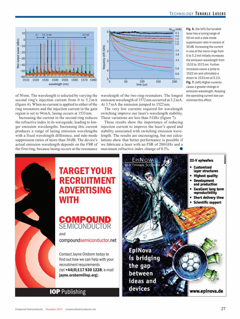
Compound Semiconductor December 2007 compoundsemiconductor.net 27
Technology T u n a b l e l a s e r s
of 50 nm. The wavelength is selected by varying the second ring’s injection current from 0 to 5.2 mA (figure 6). When no current is applied to either of the ring resonators and the injection current in the gain region is set to 94 mA, lasing occurs at 1533 nm.
Increasing the current in the second ring reduces the refractive index in its waveguide, leading to lon-ger emission wavelengths. Increasing this current produces a range of lasing emission wavelengths with a fixed wavelength difference, and side-mode suppression ratios of more than 30 dB. The device’s actual emission wavelength depends on the FSR of the first ring, because lasing occurs at the resonance
wavelength of the two ring-resonators. The longest emission wavelength of 1572 nm occurred at 3.2 mA. At 3.7 mA the emission jumped to 1522 nm.
The very low currents required for wavelength switching improve our laser’s wavelength stability. These variations are less than 5 GHz (figure 7).
These results show the importance of reducing injection current to improve the laser’s speed and stability associated with switching emission wave-length. The results are encouraging, but our calcu-lations show that better performance is possible if we fabricate a laser with an FSR of 200 GHz and a maximum refractive index change of 0.1%.
1510
0
10
–10
–20
–30
–40
–50
–601520 1530 1540 1550 1560 1570 1580
fiber
out
put p
ower
(dBm
)
wavelength (nm)
3.7 5.2 0 mA 3.2 mA
1
0
2
3
4
50 50 100 150 200
time (µs)
0.20.61.01.41.9
2.53.8
4.5
5.8
6.8
frequ
ency
drif
t (GH
z)
ΔIring (mA) Fig. 6. (far left) Our tunable laser has a tuning range of 50 nm and a side-mode suppression ratio in excess of 30 dB. Increasing the current in one of the micro-rings from 0 to 5.2 mA initially increases the emission wavelength from 1533 to 1572 nm. Further increases cause a jump to 1522 nm and ultimately a return to 1533 nm at 5.2 A. Fig. 7. (left) Higher currents cause a greater change in emission wavelength. Keeping the operating current low can minimize this effect.
� l
TARGET YOURRECRUITMENTADVERTISINGWITH
Contact Jayne Orsborn today to find out how we can help with yourrecruitment requirements (tel +44(0)117 930 1228; [email protected]).
and
M CS AD 1007 Recruit Quarter 20/11/07 13:26 Page 1
CSDec07NTT.indd 27 20/11/07 14:19:37

compoundsemiconductor.net December 2007 Compound Semiconductor28
L E D s
Dots deliver phosphor-free white lightWhite LEDs featuring indium-rich quantum dots, rather than a yellow-emitting phosphor, have been built by Hong Chen’s team from the Chinese Academy of Sciences.
“Our work provides a novel approach to casting off the limitations of a [down- converting] phosphor,” said Chen. Accord-ing to him, phosphor-free devices promise to deliver longer lifetimes and higher output efficiencies than conventional LED designs.
The researchers fabr icated their 300 μm × 300 μm LED chips by low-pressure MOCVD growth on sapphire substrates. A 3 μm thick buffer was grown, followed by 220 nm of InGaN, a four-period active region comprising 3 nm InGaN quantum wells and 14 nm GaN barriers, and a p-type region.
Transmission electron microscopy revealed spinodial decomposition of InGaN
in the quantum wells. This phase separation – enhanced by the InGaN underlayer – leads to indium-rich quantum dots with a diameter of 3–4 nm and a density of 1012 cm–2.
At LED drive currents of less than 5 mA, yellow emission from the dots dominates the device’s output. However, blue emission kicks in at higher currents and the ratio of blue-to-yellow emission intensity is almost constant between 20 and 60 mA.
This leads to a stable white light output over this current range, which makes the chip suitable for LED lighting applications. In fact, Chen says that the device can over-come the unwanted color change that plagues many phosphor-converted white LEDs when the drive current is changed.
If quantum-dot LEDs were to replace the light bulb, then their ratio of blue-to-yellow
emission intensity would have to be main-tained at higher drive currents. However, this should not be a major obstacle, because the current density through the team’s chip at 60 mA is almost identical to that of a 1 × 1 mm power chip operating at 700 mA.
One downside of the phosphor-free device is its efficacy, which is lower than 10 lm/W. The researchers are planning to develop new technology to increase quantum efficiency.
“We also need to investigate how to con-trol the ratio of blue and yellow light intensi-ties, and see whether yellow emission can be shifted to longer wavelengths,” explained Chen. If this is possible, it would improve the device’s color-rendering index.
G a N O p t O e l e c t r O n i c s
Non-polar LEDs can now deliver far higher output powers and efficiencies in the blue thanks to the efforts of Kenji Iso and co-workers at the University of California, Santa Barbara.
The team’s encapsulated LEDs are not as efficient as today’s best conventional devices (which have the handicap of strong internal polarization fields), but their brightest 468 nm emitter delivers output powers and external quantum efficiencies of 8.9 mW and 16.8% at 20 mA, and 27.6 mW and 10.4% at 100 mA.
Iso and colleagues fabricated the 300 μm × 300 μm devices using MOCVD on m-plane Mitsubishi Chemical GaN. The
substrates were polished with chemical and mechanical treatments and had a threading dislocation density of less than 5 × 106 cm–2.
Various LED epistructures were produced. These had similar designs to conventional devices but with different active regions.
The best device had a six-period multiple quantum well that featured 8 nm thick wells and 37.5 nm thick barriers.
Surprisingly, variations in the barrier’s thickness produced a 43 nm shift in peak emission wavelength. “We don’t know the reason for this,” admitted Iso.
Increasing drive current from 1 to 100 mA led to an emission blue-shift of 3.7 nm. This variation is not due to polarization-related electric fields but to the band-filling effect of deep localized energy states.
Iso believes that non-polar LEDs could provide efficient emission in the so-called “green-gap”. The team is working towards this goal by optimizing the growth condi-tions for 500 nm emitters.
UCSB ramps non-polar blue LED output power
Journal referenceK Iso et al. 2007 Jap. J. App. Phys. 40 L960.
…GaN shows multijunction potentialA US partnership led by Georgia Institute of Technology has built GaN/InGaN solar cells on sapphire substrates with internal quantum efficiencies of 60% and open circuit voltages of up to 2.4 V.
The devices could be used to improve the performance of existing terrestrial multijunction cells, which need an additional cell with a bandgap beyond 2.4 eV to boost their conversion efficiency from 40 to 50%.
The team’s MOCVD-grown cell is not optimal – it suffers from phase separation, which
reduces the open circuit voltage and the photogenerated current.
Inefficiencies also result from the semi-transparent current spreading layer that absorbs up to 40% of the incident light.
…VCSELs hit 35 Gbit/sLarry Coldren’s team from the University of California, Santa Barbara, has broken the VCSEL-based data transmission record with a
980 nm laser capable of delivering 35 Gbit/s.The design is claimed to be suitable for
mass-production and does not require any ion-implementation or regrowth steps.
High speeds resulted from a small mode volume, which was created by using a tapered oxide aperture and placing the n-type contact within five mirror pairs of the active region.
Data transmission experiments through optical fiber gave a bit error rate of 9.2 × 10⁻¹².
Research in brief…
Journal referenceO Jani 2007 Appl. Phys. Lett. 91 132117.
Technology R E s E a R c h R E v i E w
Journal referenceY-C Chang 2007 Elec. Lett. 43 1227.
The non-polar LED features a six-period InGaN/GaN multiple quantum well, an undoped AlGaN electron blocking layer and an indium tin oxide contact.
Journal referenceX H Wang 2007 Appl. Phys. Lett. 91 161912.
UC
SB
CSDec07ResearchReview.indd 28 20/11/07 14:20:15

Follow Mr Chip to register free today to get access to industry newsand reports on current developments in compound semiconductors.Visit compoundsemiconductor.net.
Take a closer look behind the headlines
Connecting the compound semiconductor community
A community website from Institute of Physics Publishing
for the inside stories in the compound semiconductor industry
M CS AD 1007 Fillers detective-2 20/11/07 14:59 Page 1
