completed edc
DESCRIPTION
EDC labTRANSCRIPT
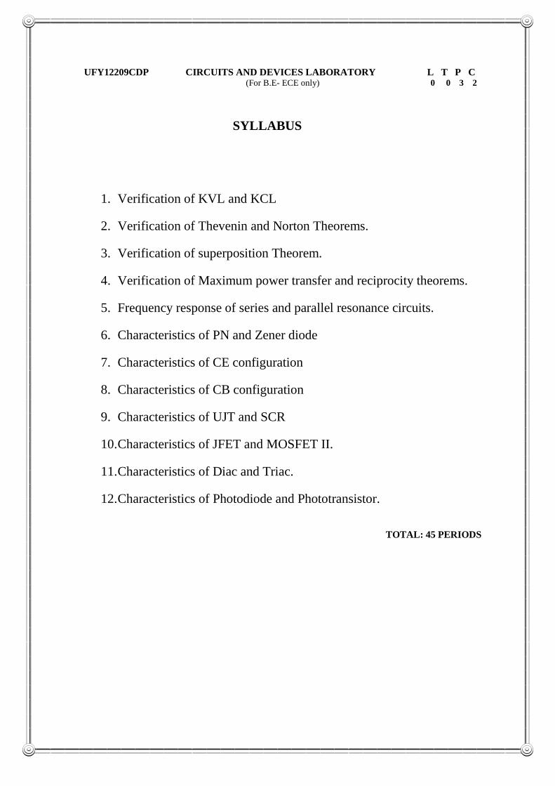
UFY12209CDP CIRCUITS AND DEVICES LABORATORY L T P C (For B.E- ECE only) 0 0 3 2
SYLLABUS
1. Verification of KVL and KCL
2. Verification of Thevenin and Norton Theorems.
3. Verification of superposition Theorem.
4. Verification of Maximum power transfer and reciprocity theorems.
5. Frequency response of series and parallel resonance circuits.
6. Characteristics of PN and Zener diode
7. Characteristics of CE configuration
8. Characteristics of CB configuration
9. Characteristics of UJT and SCR
10. Characteristics of JFET and MOSFET II.
11. Characteristics of Diac and Triac.
12. Characteristics of Photodiode and Phototransistor.
TOTAL: 45 PERIODS
2
2
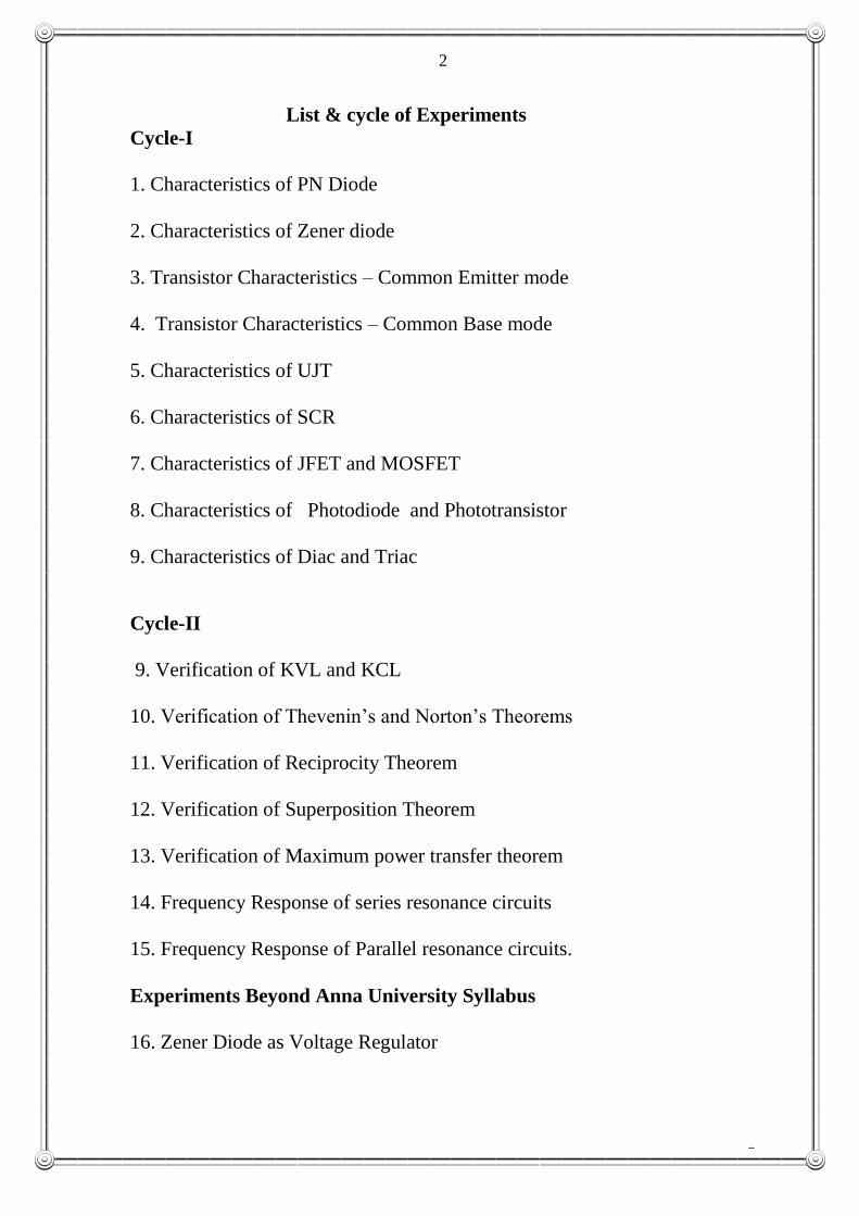
List & cycle of Experiments
Cycle-I
1. Characteristics of PN Diode
2. Characteristics of Zener diode
3. Transistor Characteristics – Common Emitter mode
4. Transistor Characteristics – Common Base mode
5. Characteristics of UJT
6. Characteristics of SCR
7. Characteristics of JFET and MOSFET
8. Characteristics of Photodiode and Phototransistor
9. Characteristics of Diac and Triac
Cycle-II
9. Verification of KVL and KCL
10. Verification of Thevenin‟s and Norton‟s Theorems
11. Verification of Reciprocity Theorem
12. Verification of Superposition Theorem
13. Verification of Maximum power transfer theorem
14. Frequency Response of series resonance circuits
15. Frequency Response of Parallel resonance circuits.
Experiments Beyond Anna University Syllabus
16. Zener Diode as Voltage Regulator
3
3
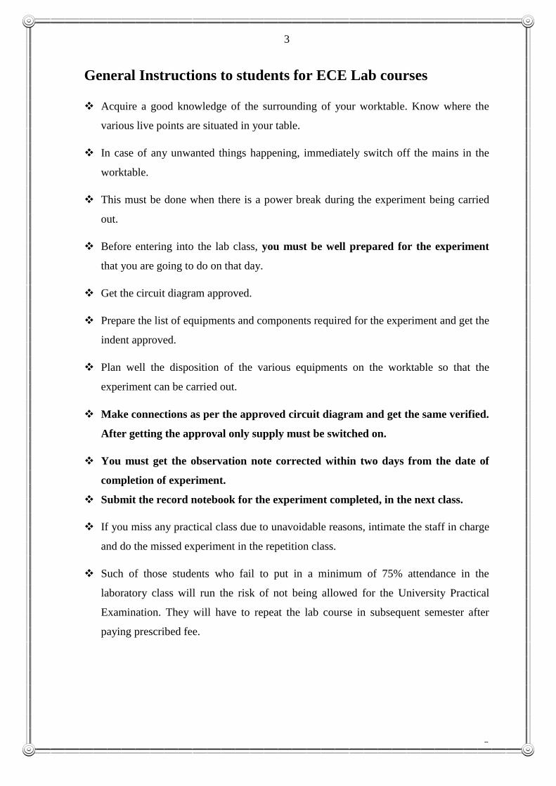
General Instructions to students for ECE Lab courses
Acquire a good knowledge of the surrounding of your worktable. Know where the
various live points are situated in your table.
In case of any unwanted things happening, immediately switch off the mains in the
worktable.
This must be done when there is a power break during the experiment being carried
out.
Before entering into the lab class, you must be well prepared for the experiment
that you are going to do on that day.
Get the circuit diagram approved.
Prepare the list of equipments and components required for the experiment and get the
indent approved.
Plan well the disposition of the various equipments on the worktable so that the
experiment can be carried out.
Make connections as per the approved circuit diagram and get the same verified.
After getting the approval only supply must be switched on.
You must get the observation note corrected within two days from the date of
completion of experiment.
Submit the record notebook for the experiment completed, in the next class.
If you miss any practical class due to unavoidable reasons, intimate the staff in charge
and do the missed experiment in the repetition class.
Such of those students who fail to put in a minimum of 75% attendance in the
laboratory class will run the risk of not being allowed for the University Practical
Examination. They will have to repeat the lab course in subsequent semester after
paying prescribed fee.
4
4
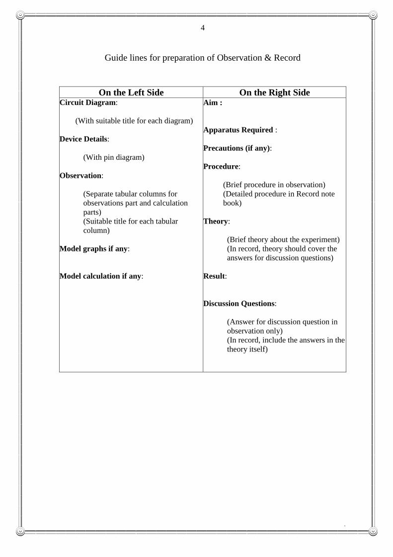
Guide lines for preparation of Observation & Record
On the Left Side On the Right Side Circuit Diagram:
(With suitable title for each diagram)
Device Details:
(With pin diagram)
Observation:
(Separate tabular columns for
observations part and calculation
parts)
(Suitable title for each tabular
column)
Model graphs if any:
Model calculation if any:
Aim :
Apparatus Required :
Precautions (if any):
Procedure:
(Brief procedure in observation)
(Detailed procedure in Record note
book)
Theory:
(Brief theory about the experiment)
(In record, theory should cover the
answers for discussion questions)
Result:
Discussion Questions:
(Answer for discussion question in
observation only)
(In record, include the answers in the
theory itself)
5
5
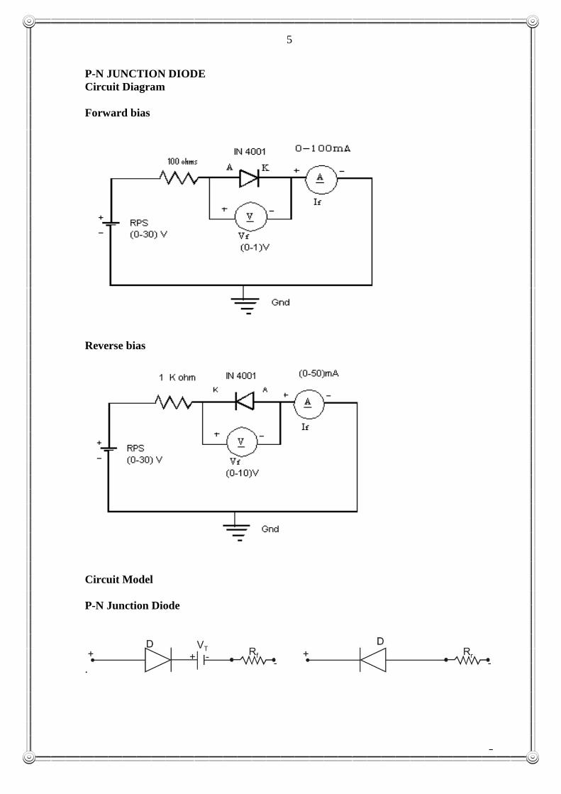
P-N JUNCTION DIODE
Circuit Diagram
Forward bias
Reverse bias
Circuit Model
P-N Junction Diode
.

6
6
Objective
To obtain the forward and reverse bias characteristics of semiconductor diode
Reference
1 “ Electronic Devices and circuits” by Salivahanan, Suresh kumar, Vallavaraj.
2 “ Principles of Electronics” by V.K. Mehta.
3 “ Basic Electronics” – A Text Lab Manual by Paul. B. Zbar and Malvino.
Knowledge Required
P-N Junction, depletion layer, barrier potential, forward bias, reverse bias, break
down voltage, Avalanche breakdown.
Precaution
Voltage level should not exceed the value specified for the device.
Procedure
For various values of forward and reverse biased voltages, tabulate the values of
currents.
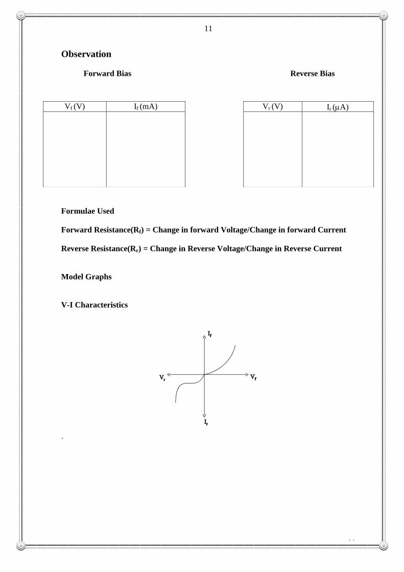
1. Characteristics of PN Diode
7
7
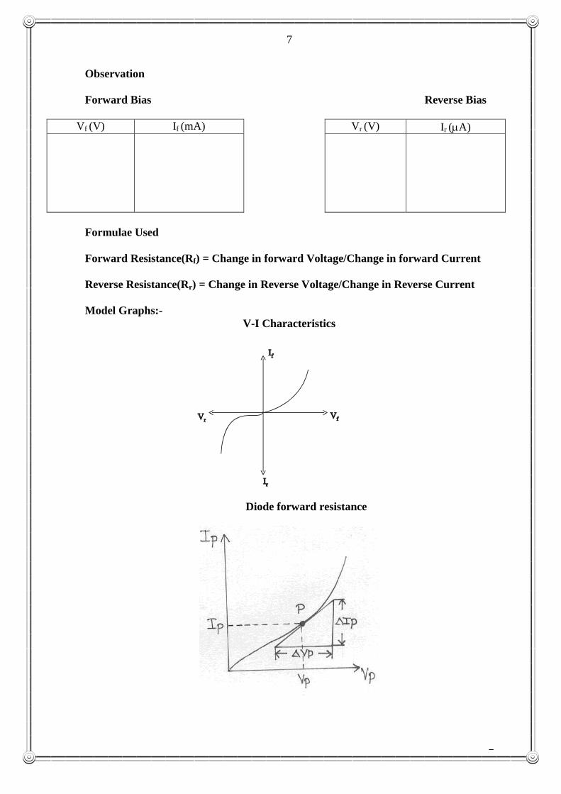
Observation
Forward Bias Reverse Bias
Vf (V) If (mA) Vr (V) Ir (A)
Formulae Used
Forward Resistance(Rf) = Change in forward Voltage/Change in forward Current
Reverse Resistance(Rr) = Change in Reverse Voltage/Change in Reverse Current
Model Graphs:-
V-I Characteristics
Diode forward resistance

8
8
Result
The forward and reverse bias characteristics of semiconductor diode are plotted.
Forward Resistance = ______________
Discussion Questions
1. What are Intrinsic and Extrinsic Semiconductors?
2. Define Peak Inverse Voltage.
3. What do you mean by potential barrier in a PN Junction?
4. What are N – type and P – type semiconductors?
5. What are the applications of semiconductor diode?
6. What are Donors and Acceptors in semiconductors?
7. Define doping.
********************************************************************
9
9
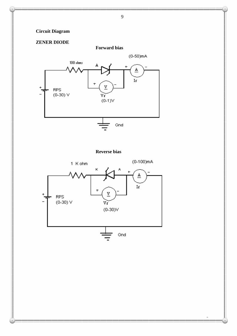
Circuit Diagram
ZENER DIODE
Forward bias
Reverse bias
10
10
Objective
To obtain the forward and reverse bias characteristics of zener diode
Reference
1.“ Electronic Devices and circuits” by Salivahanan, Suresh kumar, Vallavaraj.
2.“ Principles of Electronics” by V.K. Mehta.
3.“ Basic Electronics” – A Text Lab Manual by Paul. B. Zbar and Malvino.
Knowledge Required
P-N Junction, depletion layer, barrier potential, forward bias, reverse bias, break
down voltage, zener breakdown, Avalanche breakdown.
Precaution
Voltage level should not exceed the value specified for the device.
Procedure
For various values of forward and reverse biased voltages, tabulate the values of
currents.
2. Characteristics of Zener Diode
11
11
Observation
Forward Bias Reverse Bias
Formulae Used
Forward Resistance(Rf) = Change in forward Voltage/Change in forward Current
Reverse Resistance(Rr) = Change in Reverse Voltage/Change in Reverse Current
Model Graphs
V-I Characteristics
.
Vf (V) If (mA) Vr (V) Ir (A)

12
12
Result
The forward and reverse bias characteristics of Zener diode is plotted.
Forward Resistance = ______________
Reverse Resistance = ______________
Discussion Questions
1. What are the applications of Zener diode?
2. How does a Zener diode act as voltage regulator?
3. In What way Zener Diode is different from PN junction Diode?
4. What do you mean by avalanche breakdown voltage?
5. What do you mean by Leakage current?
***********************************************************
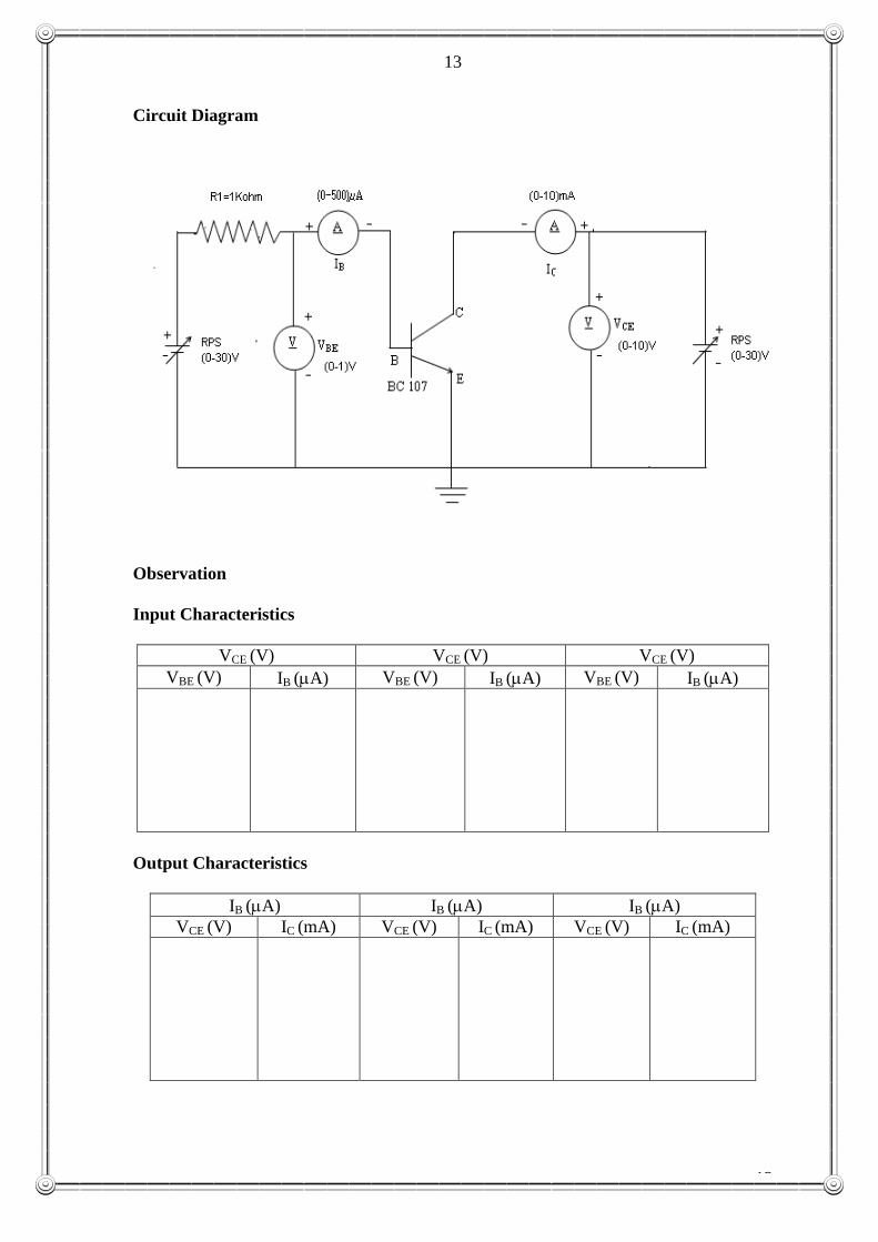
13
13
Circuit Diagram
Observation
Input Characteristics
VCE (V) VCE (V) VCE (V)
VBE (V) IB (A) VBE (V) IB (A) VBE (V) IB (A)
Output Characteristics
IB (A) IB (A) IB (A)
VCE (V) IC (mA) VCE (V) IC (mA) VCE (V) IC (mA)
14
14
Objective
To obtain the characteristic curves for a transistor in common emitter mode
and hence to determine the h-parameters.
Reference
1. “Electronic devices and circuits” by Salivahanan, Suresh kumar, Vallavaraj
2. “Principles of Electronics” by V.K.Mehta
Knowledge required
Composition of transistor, types of transistors, transistor biasing, Working of
transistor, types of circuit connections for operating a transistor, forward biased
diode characteristic, knee voltage.
Precautions
1. Polarities of the bias voltage should be correct.
2. Voltage and current levels should not exceed the values specified for the device.
3. Both rheostats should be kept in minimum position at the time of switching on
the supply.
Procedure
Input Characteristics
Keeping the voltage across Collector to Emitter (VCE) as constant, tabulate the
values of base current for various values of Base-Emitter voltage (VBE).
Repeat the same procedure for various constant values of VCE.
Output Characteristics
Keeping the base current as constant, tabulate the values of collector current
(IC) for various values of Collector-Emitter voltage (VCE).
Repeat the same procedure for various constant values of base current (IB).
3. Transistor Characteristics-Common Emitter Mode
15
15
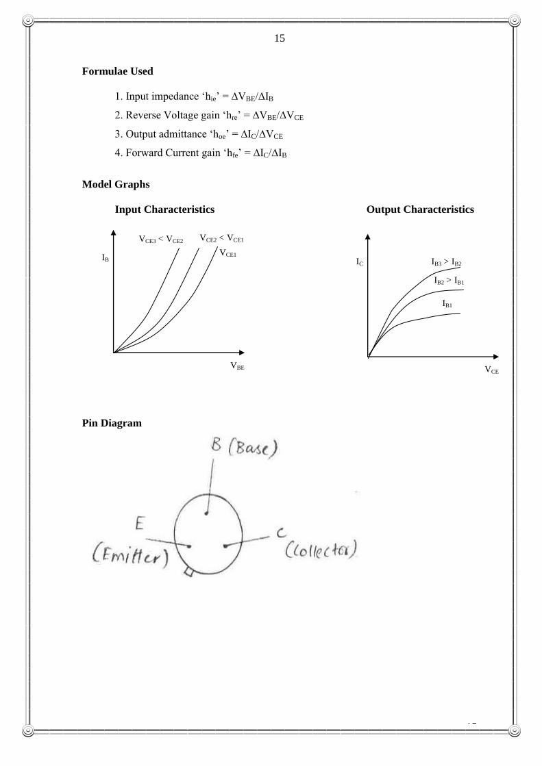
Formulae Used
1. Input impedance „hie‟ = ∆VBE/∆IB
2. Reverse Voltage gain „hre‟ = ∆VBE/∆VCE
3. Output admittance „hoe‟ = ∆IC/∆VCE
4. Forward Current gain „hfe‟ = ∆IC/∆IB
Model Graphs
Input Characteristics Output Characteristics
Pin Diagram
VCE3 < VCE2
VCE1
VCE2 < VCE1
VBE
IB IB3 > IB2
IB1
IB2 > IB1
VCE
IC

16
16
Result
The input and output characteristics of CE transistor configuration are drawn.
Parameters Practical value
hie
hfe
hoe
hre
Discussion Questions
1. What is mean by biasing?
2. Why the BJT is called as current controlled device?
3. What are the different operating regions?
4. Define the base width modulation or early effect.
5. What is secondary breakdown?
******************************************************************
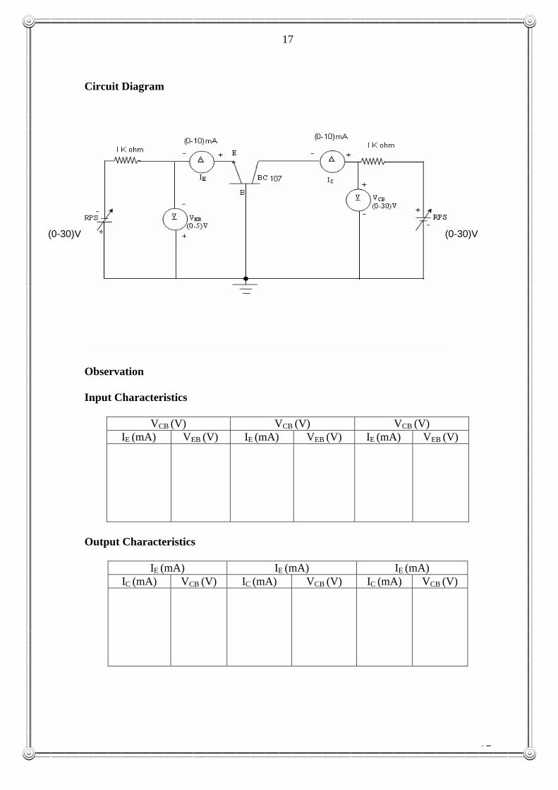
17
17
Circuit Diagram
Observation
Input Characteristics
VCB (V) VCB (V) VCB (V)
IE (mA) VEB (V) IE (mA) VEB (V) IE (mA) VEB (V)
Output Characteristics
IE (mA) IE (mA) IE (mA)
IC (mA) VCB (V) IC (mA) VCB (V) IC (mA) VCB (V)
(0-30)V (0-30)V
18
18
Objective
To obtain the characteristic curves for a transistor in common base mode and
hence to determine the h-parameters.
Reference
1. “Electronic devices and circuits” by Salivahanan, Suresh kumar, Vallavaraj
2. “Principles of Electronics” by V.K.Mehta
Knowledge required
Composition of transistor, types of transistors, transistor biasing, working of
transistor, types of circuit connections for operating a transistor, forward biased diode
characteristic, knee voltage.
Precautions
1. Polarities of the bias voltage should be correct.
2. Voltage and current levels should not exceed the values specified for the
device.
3. Both rheostats should be kept in minimum position at the time of switching on
the supply.
Procedure
Input Characteristics
Keeping the voltage across Collector to Base (VCB) as constant, tabulate the
values of emitter current IE, for various values of Emitter- Base voltage (VEB).
Repeat the same procedure for various constant values of VCB.
Output Characteristics
Keeping the emitter current IE as constant, tabulate the values of collector
current IC, for various values of Collector-Base voltage (VCB).
Repeat the same procedure for various constant values of emitter current IE.
4. Transistor Characteristics-Common Base Mode
19
19
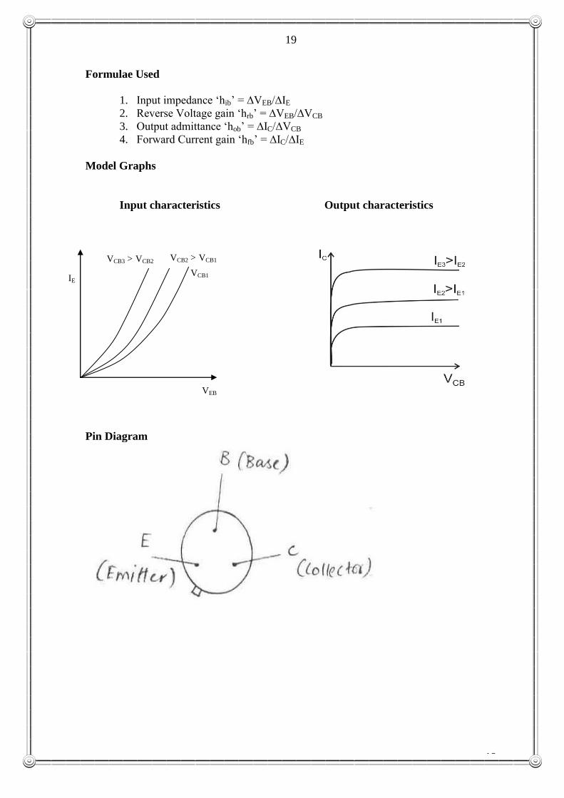
Formulae Used
1. Input impedance „hib‟ = ∆VEB/∆IE
2. Reverse Voltage gain „hrb‟ = ∆VEB/∆VCB
3. Output admittance „hob‟ = ∆IC/∆VCB
4. Forward Current gain „hfb‟ = ∆IC/∆IE
Model Graphs
Input characteristics Output characteristics
Pin Diagram
VCB3 > VCB2
VCB1
VCB2 > VCB1
VEB
IE

20
20
Result
The input and output characteristics of CB transistor configuration are drawn.
Parameters Practical value
hib
hfb
hob
hrb
Discussion Questions
1. Compare the various configurations of transistor based on the following headings
(a) voltage gain
(b) input resistance
(c) output resistance
(d) application
2. What is the main advantage of CE over CB configuration?
3. Write the relationship between , , .
************************************************************************
21
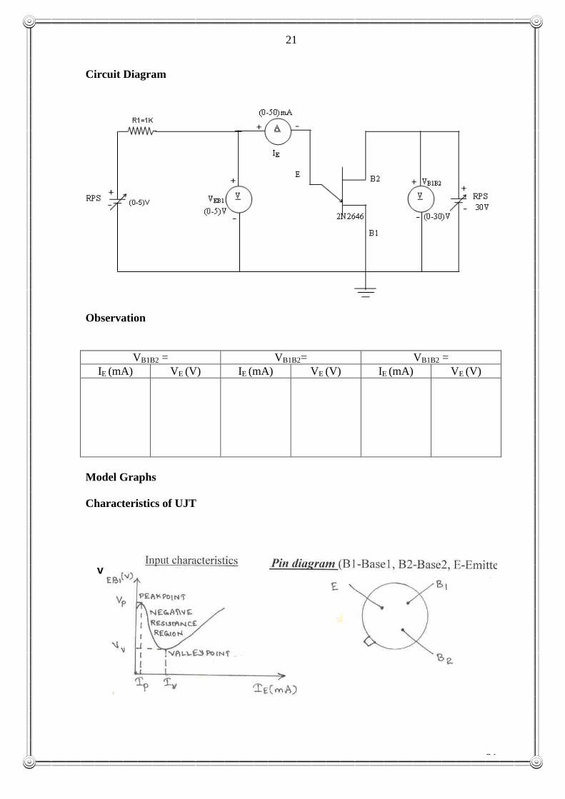
21
Circuit Diagram
Observation
VB1B2 = VB1B2= VB1B2 =
IE (mA) VE (V) IE (mA) VE (V) IE (mA) VE (V)
Model Graphs
Characteristics of UJT
22
22
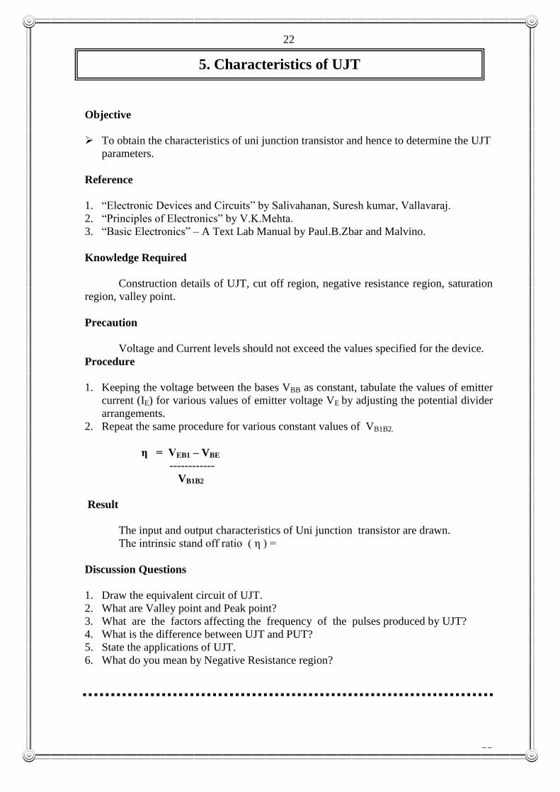
Objective
To obtain the characteristics of uni junction transistor and hence to determine the UJT
parameters.
Reference
1. “Electronic Devices and Circuits” by Salivahanan, Suresh kumar, Vallavaraj.
2. “Principles of Electronics” by V.K.Mehta.
3. “Basic Electronics” – A Text Lab Manual by Paul.B.Zbar and Malvino.
Knowledge Required
Construction details of UJT, cut off region, negative resistance region, saturation
region, valley point.
Precaution
Voltage and Current levels should not exceed the values specified for the device.
Procedure
1. Keeping the voltage between the bases VBB as constant, tabulate the values of emitter
current (IE) for various values of emitter voltage VE by adjusting the potential divider
arrangements.
2. Repeat the same procedure for various constant values of VB1B2.
η = VEB1 – VBE
------------
VB1B2
Result
The input and output characteristics of Uni junction transistor are drawn.
The intrinsic stand off ratio ( η ) =
Discussion Questions
1. Draw the equivalent circuit of UJT.
2. What are Valley point and Peak point?
3. What are the factors affecting the frequency of the pulses produced by UJT?
4. What is the difference between UJT and PUT?
5. State the applications of UJT.
6. What do you mean by Negative Resistance region?
5. Characteristics of UJT
23
23

24
24
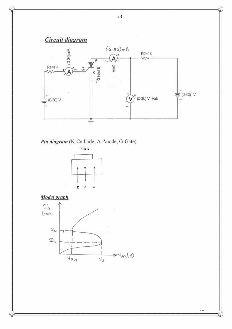
Objective
To find the latching and holding current of a given SCR
Reference
1.“Electronic Devices and Circuits” by Salivahanan, Suresh kumar,
Vallavaraj.
2. “Principles of Electronics” by V.K.Mehta.
3. “Basic Electronics” – A Text Lab Manual by Paul.B.Zbar and Malvino.
Knowledge Required
Construction details of SCR, gate current and breakover voltage.
Precaution
Voltage and Current levels should not exceed the values specified for the device.
Procedure
1. Check the RPS connecting the circuit.
2. Connect the circuit as per the circuit diagram
3. Set the gate current Ig equal to firing current vary anode the cathode voltage.
VAK in steps of 1V and note down the corresponding anode current IA.
4. VBRF is the point where voltage (VAK) suddenly drops and hence there is a sudden
increase in anode current IA.
5. Increase the VAK in steps and note down the IA.
6. Open the gate and decrease VAK.
6. Characteristics of SCR

25
25
Tabulation
IG= ----- (mA)
Sl.No. VAK.(v) IA (mA)
26
26
Result
The Characteristics of SCR is drawn.
Forward break over voltage(VBRF ) =
Latching current (IL ) =
Holding current (IH) =
Discussion Questions:
1.What is the purpose of gate current in SCR?
2.Define Holding current
3.Specify the methods of turning on SCR.
4.What is the difference between SCR & Diode?
5.Define Latching current.
******************************************************************
27
27
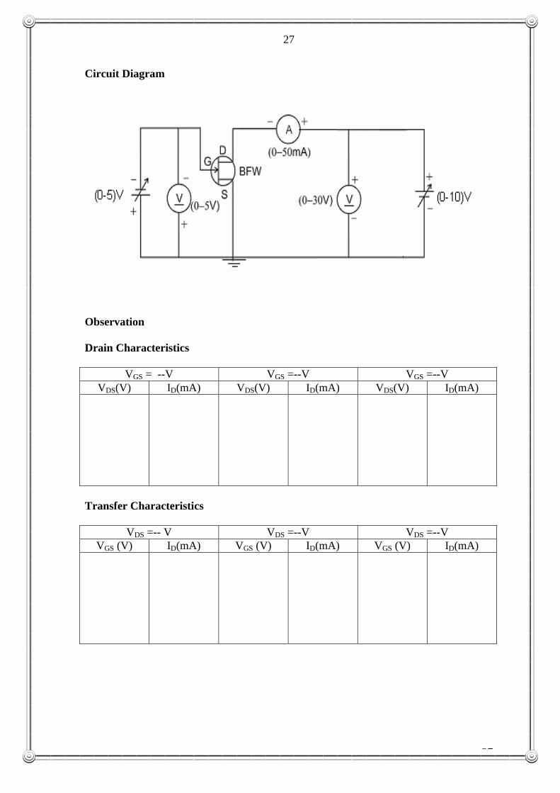
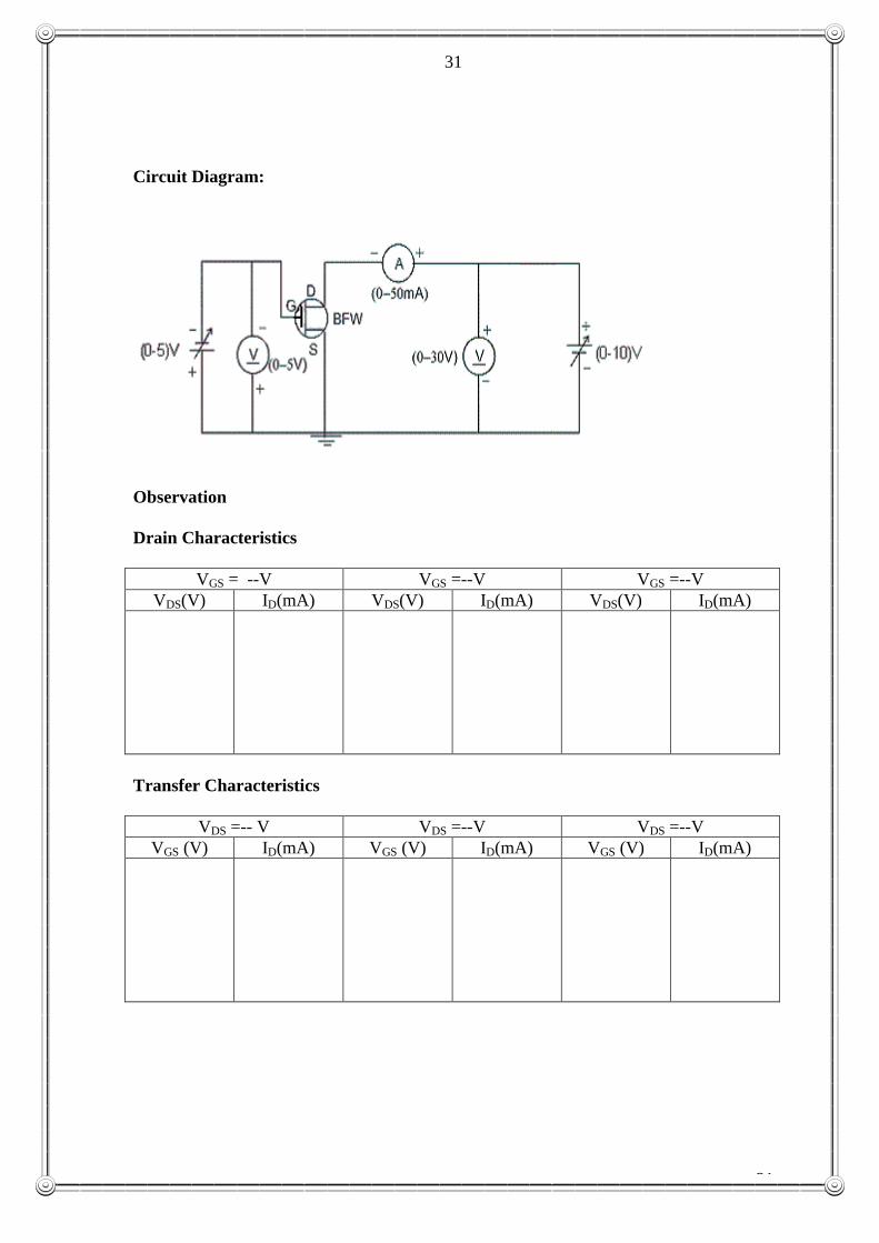
Circuit Diagram
Observation
Drain Characteristics
VGS = --V VGS =--V VGS =--V
VDS(V) ID(mA) VDS(V) ID(mA) VDS(V) ID(mA)
Transfer Characteristics
VDS =-- V VDS =--V VDS =--V
VGS (V) ID(mA) VGS (V) ID(mA) VGS (V) ID(mA)
28
28
Objective
To obtain the characteristics of junction field effect transistor and hence to
determine the FET parameters.
Reference
1. “Electronic Devices and Circuits” by Salivahanan, Suresh kumar, Vallavaraj.
2. “Principles of Electronics” by V.K.Mehta.
3. “Basic Electronics” – A Text Lab Manual by Paul.B.Zbar and Malvino.
Knowledge Required
Pinch off voltage, Gate-source cut off voltage.
Precaution
Voltage and Current levels should not exceed the values specified for the device.
Procedure
Drain Characteristics
1. Keeping the values of Gate-source voltage VGS, as constant, tabulate the
values of drain current (ID), for various values of drain-source voltage VDS.
2. Repeat the same procedure for various constant values of VGS.
Transfer Characteristics
1. Keeping the values of Drain-source voltage VDS, as constant, tabulate the
values of drain current (ID) for various values of VGS.
2. Repeat the same procedure for various constant values of VDS.
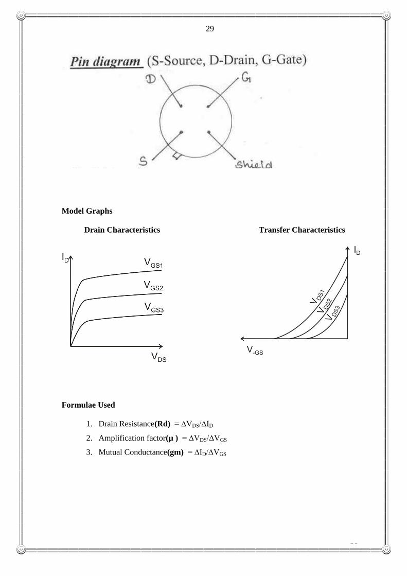
7(a). Characteristics of JFET
29
29
Model Graphs
Drain Characteristics Transfer Characteristics
Formulae Used
1. Drain Resistance(Rd) = ∆VDS/∆ID
2. Amplification factor(µ ) = ∆VDS/∆VGS
3. Mutual Conductance(gm) = ∆ID/∆VGS
30
30
Result
The drain and transfer characteristics of Junction field effect Transistor are
drawn and the parameters obtained are
(i) Dynamic drain resistance (Rd) =
(ii) Mutual conductance(gm) =
(iii) Amplification factor(µ ) =
Discussion Questions
1. What are the differences between JFET and MOSFET?
2. Define pinch off voltage.
3. What are the modes of operation available in JFET?
4. Why JFET is called as a voltage controlled device?
5. What is the difference between FET and BJT?
************************************************************************
31
31
Circuit Diagram:
Observation
Drain Characteristics
VGS = --V VGS =--V VGS =--V
VDS(V) ID(mA) VDS(V) ID(mA) VDS(V) ID(mA)
Transfer Characteristics
VDS =-- V VDS =--V VDS =--V
VGS (V) ID(mA) VGS (V) ID(mA) VGS (V) ID(mA)

32
32
Objective
To obtain the characteristics of junction Metal Oxide Semiconductor field effect
transistor and hence to determine the MOSFET parameters.
Reference
4. “Electronic Devices and Circuits” by Salivahanan, Suresh kumar, Vallavaraj.
5. “Principles of Electronics” by V.K.Mehta.
6. “Basic Electronics” – A Text Lab Manual by Paul.B.Zbar and Malvino.
Knowledge Required
Pinch off voltage, Gate-source cut off voltage.
Precaution
Voltage and Current levels should not exceed the values specified for the device.
Procedure
Drain Characteristics
3. Keeping the values of Gate-source voltage VGS, as constant, tabulate the
values of drain current (ID), for various values of drain-source voltage VDS.
4. Repeat the same procedure for various constant values of VGS.
Transfer Characteristics
3. Keeping the values of Drain-source voltage VDS, as constant, tabulate the
values of drain current (ID) for various values of VGS.
4. Repeat the same procedure for various constant values of VDS.
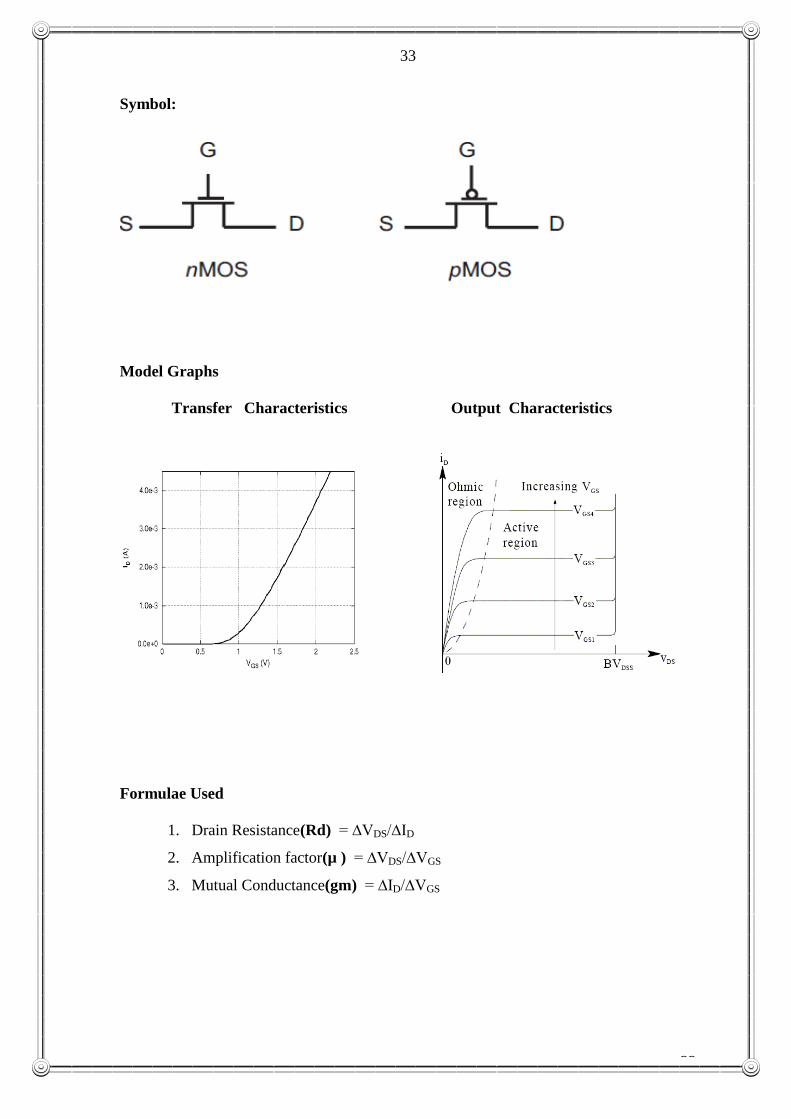
7(b). Characteristics of MOSFET
33
33
Symbol:
Model Graphs
Transfer Characteristics Output Characteristics
Formulae Used
1. Drain Resistance(Rd) = ∆VDS/∆ID
2. Amplification factor(µ ) = ∆VDS/∆VGS
3. Mutual Conductance(gm) = ∆ID/∆VGS

34
34
Result
The drain and transfer characteristics of Metal Oxide Semiconductor field
effect Transistor are drawn and the parameters obtained are
(iv) Dynamic drain resistance (Rd) =
(v) Mutual conductance(gm) =
(vi) Amplification factor(µ ) =
Discussion Questions
1. What are the differences between JFET and MOSFET?
2. Define pinch off voltage.
3. What are the modes of operation available in MOSFET?
4. Why MOSFET is called as a voltage controlled device?
5. What is the difference between MOSFET and BJT?
6. Why MOSFET is called insulated gate FET?
7. What is N-channel and P-channel MOSFET?
8. Differentiate Enhancement and Depletion types of MOSFETs.
9. Is it possible for a Depletion type of MOSFET to operate in both modes?
10. What are the disadvantages of MOSFET type and why V-MOS is developed?
************************************************************************
35
35
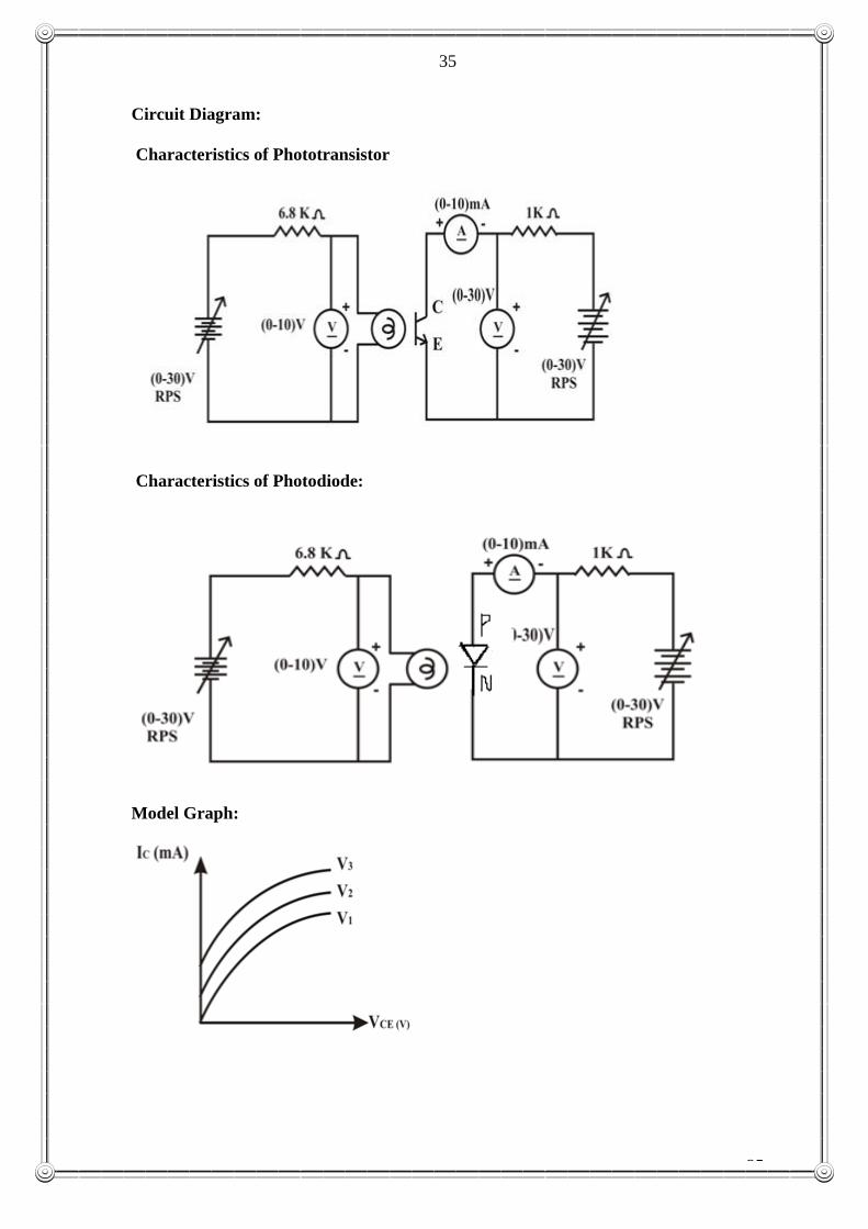
Circuit Diagram:
Characteristics of Phototransistor
Characteristics of Photodiode:
Model Graph:

36
36
Objective
To obtain the characteristics of Photodiode
Reference
1. “Electronic Devices and Circuits” by Salivahanan, Suresh kumar, Vallavaraj.
2. “Principles of Electronics” by V.K.Mehta.
3. “Basic Electronics” – A Text Lab Manual by Paul.B.Zbar and Malvino.
Knowledge Required
Construction and operation of Photodiode.
Precaution 1.Polarities of the bias voltage should be correct.
2.Volatge and current levels should not exceed the values specified for the device.
Procedure
1.Select Photodiode.
2.Connect the circuit as per the circuit diagram.
3.For different values of voltage, note the corresponding current.
4. The same procedure is repeated for Dark, Dim and Bright conditions.
8. Characteristics of Photodiode and Phototransistor

37
37
Observation :( Phototransistor)
DARK DIM BRIGHT
VD(V) ID(µA) VD(V) ID(µA) VD(V) ID(µA)
Observation :( Photodiode)
DARK DIM BRIGHT
VD(V) ID(µA) VD(V) ID(µA) VD(V) ID(µA)

38
38
Result
The characteristics of photodiode and phototransistor were plotted.
Discussion Questions
1. What is meant by Photodiode?
2. What is meant by dark current?
3. What are the applications of Dark current?
4. What are the differences between photodiode and transistor?
5. What are the applications of Photo Transistor?
********************************************************************
39
39
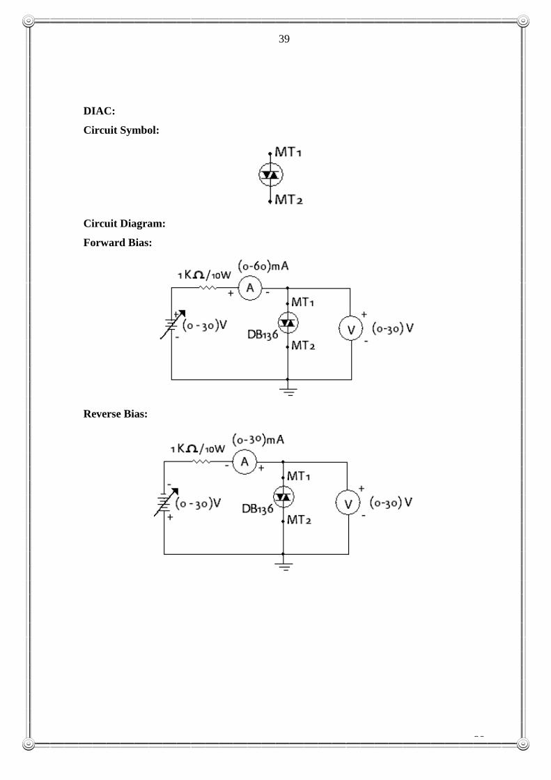
DIAC:
Circuit Symbol:
Circuit Diagram:
Forward Bias:
Reverse Bias:
40
40
Objective
To obtain the characteristics of DIAC and TRIAC
Reference
7. “Electronic Devices and Circuits” by Salivahanan, Suresh kumar, Vallavaraj.
8. “Principles of Electronics” by V.K.Mehta.
9. “Basic Electronics” – A Text Lab Manual by Paul.B.Zbar and Malvino.
Knowledge Required
Bidirectional Trigger Diode, Holding Current,Thyristor
Precaution
Voltage and Current levels should not exceed the values specified for the device.
Procedure
DIAC:
1.Connections are given as per the circuit diagram.
1. The power supply is varied in constant steps and the corresponding voltage
and current readings are noted down.
2. For particular values of applied forward voltage , the current increases. Then
the voltage across DIAC decreases with increase in current.
3. The same procedure is repeated for reverse voltage of DIAC.
4. The VI characteristics is drawn from the tabulated readings.
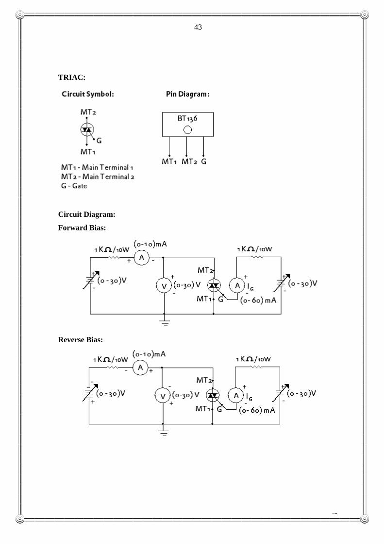
TRIAC:
1. Connections are given as per the circuit diagram.
2. Set the value of IG to be constant by adjusting the power supply.
3. The terminal voltage is varied in steps and the corresponding readings are
noted down.
4. The same procedure is repeated for reverse polarity of TRIAC.
5. The voltage and current readings are noted down.
6. The characteristics curve is plotted for the tabulated readings.
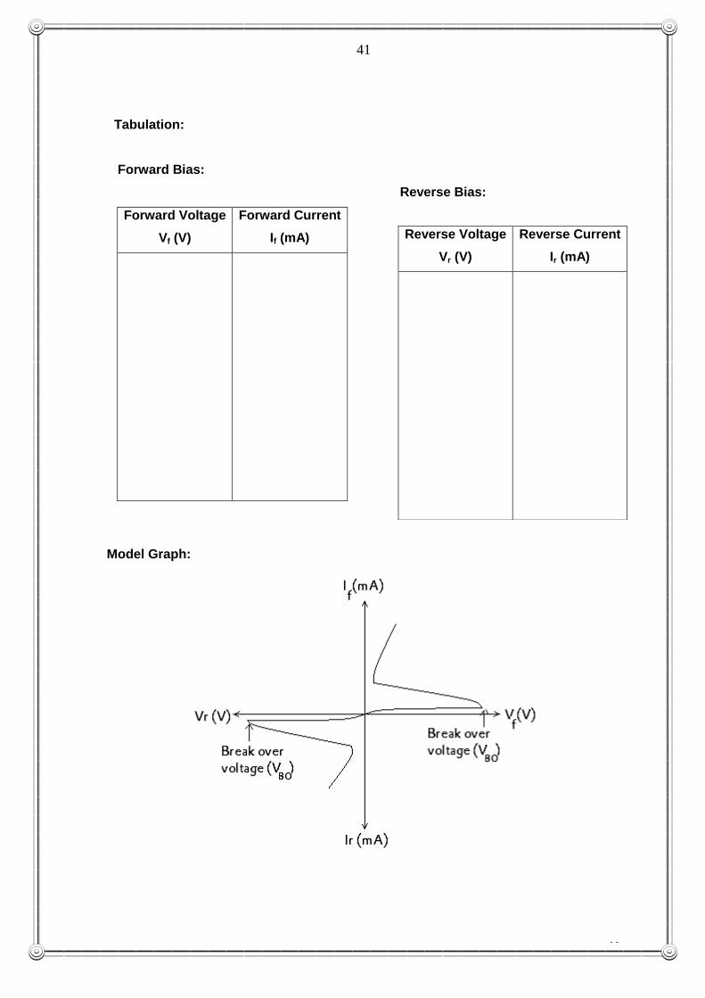
9. Characteristics of DIAC and TRIAC
41
41
Tabulation:
Forward Bias:
Reverse Bias:
Forward Voltage
Vf (V)
Forward Current
If (mA)
Model Graph:
Reverse Voltage
Vr (V)
Reverse Current
Ir (mA)

42
42
43
43
TRIAC:
Circuit Diagram:
Forward Bias:
Reverse Bias:

44
44
45
45
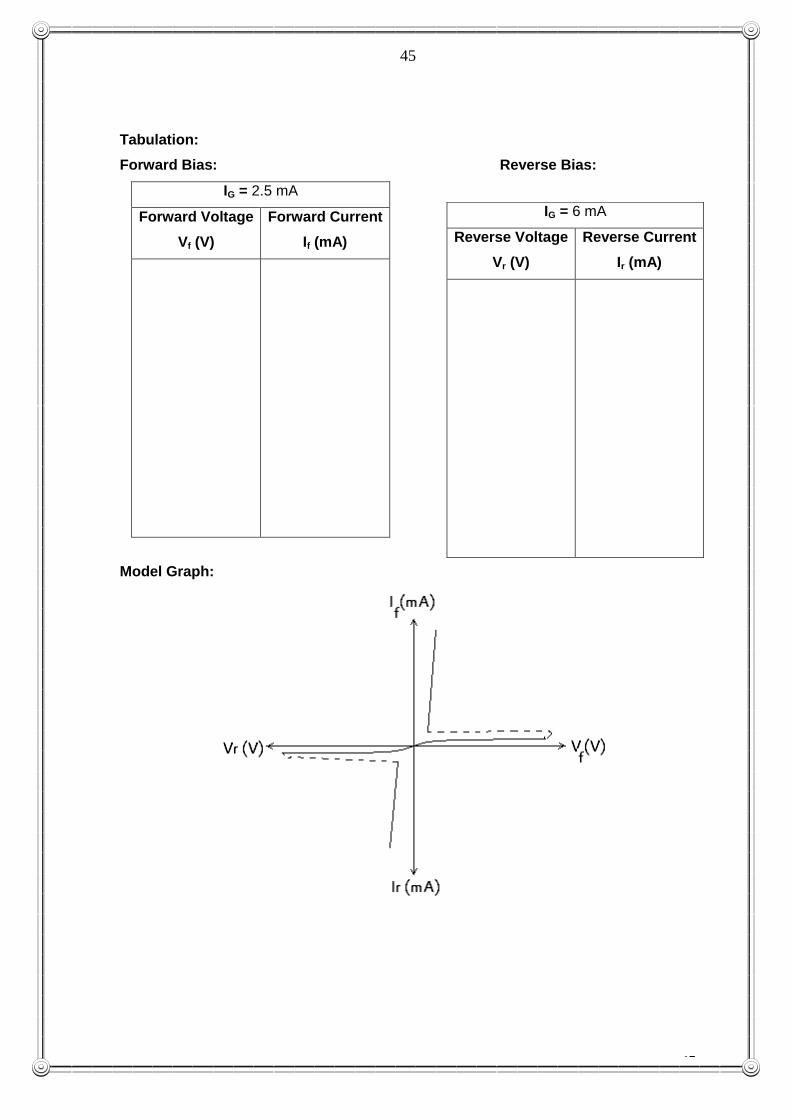
Tabulation:
Forward Bias: Reverse Bias:
IG = 2.5 mA
Forward Voltage
Vf (V)
Forward Current
If (mA)
Model Graph:
IG = 6 mA
Reverse Voltage
Vr (V)
Reverse Current
Ir (mA)
46
46
Result
The forward and reverse bias characteristics of DIAC and TRIAC are plotted.
Questions for Discussion:
1. Why the DIAC is said to be a symmetrical trigger diode?
2. Draw the SCR equivalent circuit of TRIAC.
3. How can you control the phase using TRIAC?
4. Give few applications of DIAC.
5. Give few applications of TRIAC
47
47
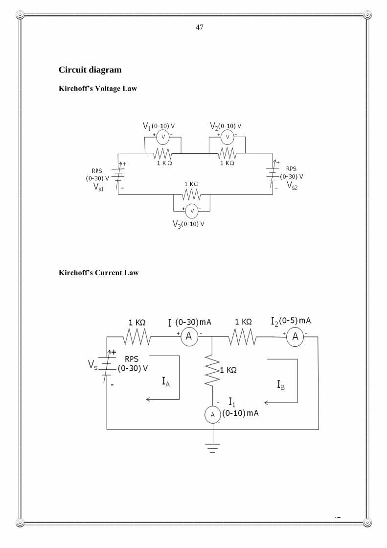
Circuit diagram
Kirchoff’s Voltage Law
Kirchoff’s Current Law
48
48
9.Verification of Kirchoff’s Voltage and Current Laws
Objective
To verify the Kirchoff‟s laws with the help of simple D.C series and parallel
circuits.
Reference
1. Electric circuit Theory, M.Arumugam and N.Premkumar
1. Electric circuits, Joseph A.Edminister
2. “Basic Electricity” Text Lab Manual, Paul .B Zhar and Gordon Rockmaker
Knowledge Required
Basic circuit laws [Ohm‟s law & Kirchoff‟s laws]
Concept of series and parallel circuits
Use of double tube rheostats, other equipments and meters
Selection of meter ranges, fuse rating
Precautions
The branch currents should not exceed the device ratings.
The ammeter and voltmeter ranges should be properly chosen.
LAWS
i) Kirchoff‟s Voltage Law
Kirchoff‟s voltage law states that the algebraic sum of all branch voltages around a closed
loop of a network is zero at all instant of time. Kirchoff‟s voltage law deals with the
element voltages in a loop. A loop is a closed path formed by two or more circuit
elements. While applying KVL to a particular loop first assign a reference direction to
each element voltage for example, assign +ve sign to the voltages if they correspond to
voltage drops and assign –ve sign to the voltages if they correspond to voltage rises.
ii) Kirchoff‟s Current Law
Kirchoff‟s current law states that the algebraic sum of the branch currents at the node is
zero at all instants of time. It deals with the element currents meeting at a node. While
applying KCL to a particular node, first assign a reference direction to each element
current for example, assign +ve sign to those currents whose direction points away from
the node. Similarly assign –ve sign to those currents whose direction points towards the
node.
49
49
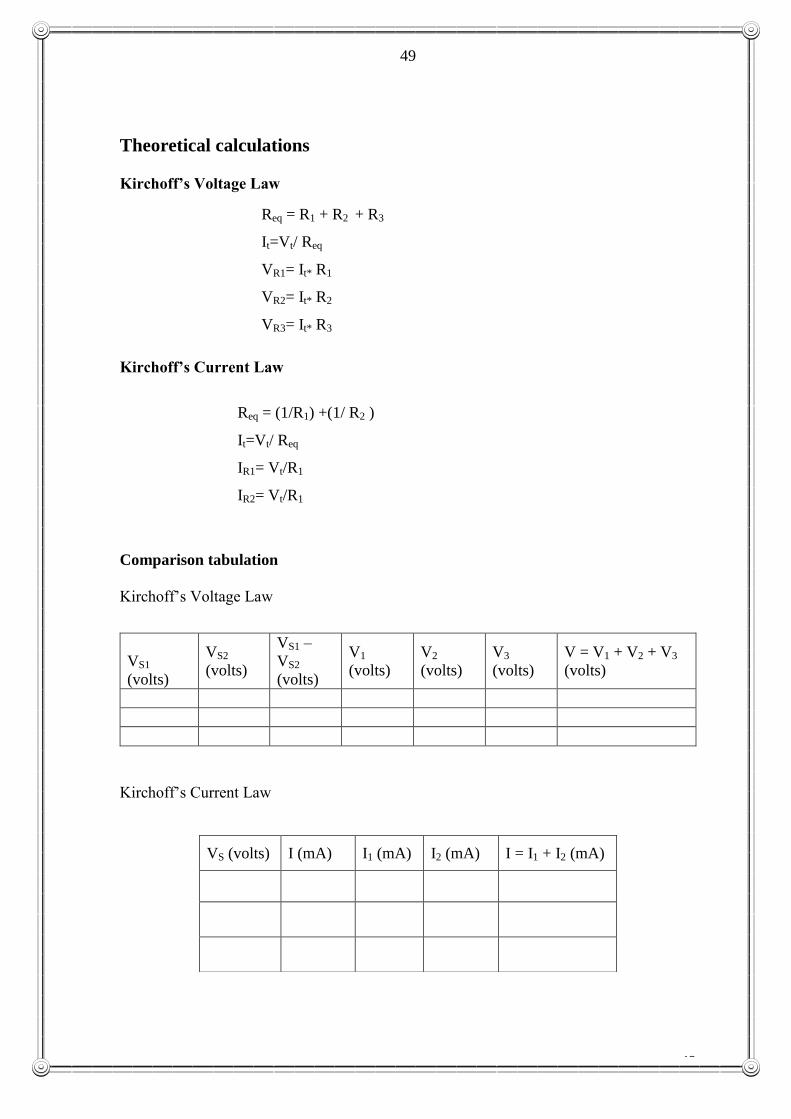
Theoretical calculations
Kirchoff’s Voltage Law
Kirchoff’s Current Law
Comparison tabulation
Kirchoff‟s Voltage Law
VS1
(volts)
VS2
(volts)
VS1 –
VS2
(volts)
V1
(volts)
V2
(volts)
V3
(volts)
V = V1 + V2 + V3
(volts)
Kirchoff‟s Current Law
VS (volts) I (mA) I1 (mA) I2 (mA) I = I1 + I2 (mA)
Req = R1 + R2 + R3
It=Vt/ Req
VR1= It* R1
VR2= It* R2
VR3= It* R3
Req = (1/R1) +(1/ R2 )
It=Vt/ Req
IR1= Vt/R1
IR2= Vt/R1
50
50
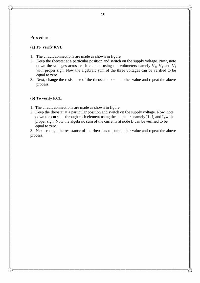
Procedure
(a) To verify KVL
1. The circuit connections are made as shown in figure.
2. Keep the rheostat at a particular position and switch on the supply voltage. Now, note
down the voltages across each element using the voltmeters namely V1, V2 and V3
with proper sign. Now the algebraic sum of the three voltages can be verified to be
equal to zero.
3. Next, change the resistance of the rheostats to some other value and repeat the above
process.
(b) To verify KCL
1. The circuit connections are made as shown in figure.
2. Keep the rheostat at a particular position and switch on the supply voltage. Now, note
down the currents through each element using the ammeters namely I1, I2 and I3 with
proper sign. Now the algebraic sum of the currents at node B can be verified to be
equal to zero.
3. Next, change the resistance of the rheostats to some other value and repeat the above
process.

51
51
Result Comparing the observed values and the theoretical values, we infer that they are
almost equal. Thus Kirchoff‟s law is verified both theoretically and practically.
Discussion Questions
1. State Ohm‟s law and Kirchoff‟s laws.
2. Distinguish between mesh and loop.
3. What are active and passive elements?
4. Can we use MI meters in d.c. circuits? Justify your answer.
5. What will happen on reversing the polarities of the MC meter terminals?
**********************************************************
52
52
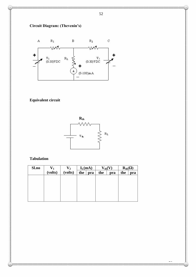
Circuit Diagram: (Thevenin’s)
Equivalent circuit
Rth
Tabulation
Sl.no V1
(volts)
V2
(volts)
IL(mA) Vth(V) Rth(Ω)
the pra the pra the pra
53
53
10. Thevenin’s and Norton’s Theorems
Objective
To obtain the Thevenin‟s and Norton‟s equivalent of the given circuit and hence
to verify these theorems with the equivalent circuits.
References
“Electric Circuit Theory” by Arumugam & Premkumar
“Electric Circuits” by Joseph A. Edminister
“Basic Electricity - A Text Lab Manual” by Paul B. Zbar and Gordon Rockmaker
Knowledge Required
Theorems – statement and their explanation.
Basic circuit laws
Selection of meter ranges, fuse ratings
THEVENIN‟S Theorem An linear active network containing linear impedances and voltage sources can be
replaced by an equivalent circuit consisting of voltage source (Vth) acting in series with an
impedance (Zth). The voltage source is the Thevenin‟s voltage (Vth) at open circuit
condition and hence also called open circuit voltage and impedance is the driving point
impedance at the terminals when all the voltage sources are removed and called as
Thevenin‟s impedance (Zth).
It is used to find the current through a particular element in a general network which
may consists of several elements along with the number of voltage and current sources.
Procedure 1. The circuit connections are given as shown in figure. The variable resistances
are initially adjusted to some suitable values. The supply voltages are
adjusted to some values V1&V2 and the current through the branch BE is
measured using the ammeter present in that branch.
2. Next, the load RL is removed from the circuit. The open circuit voltage
between B&E is measured using the proper voltage range of the multimeter.
This reading gives the value of the Thevenin‟s voltage (Vth).
3. In order to find Thevenin‟s resistance Rth, the branch BE is shorted through
an ammeter and
the short circuit current ISC is measured. Now, Rth = Vth/ISC. The value of the
current through RL is calculated as
Lth
thL
RR
VI
54
54
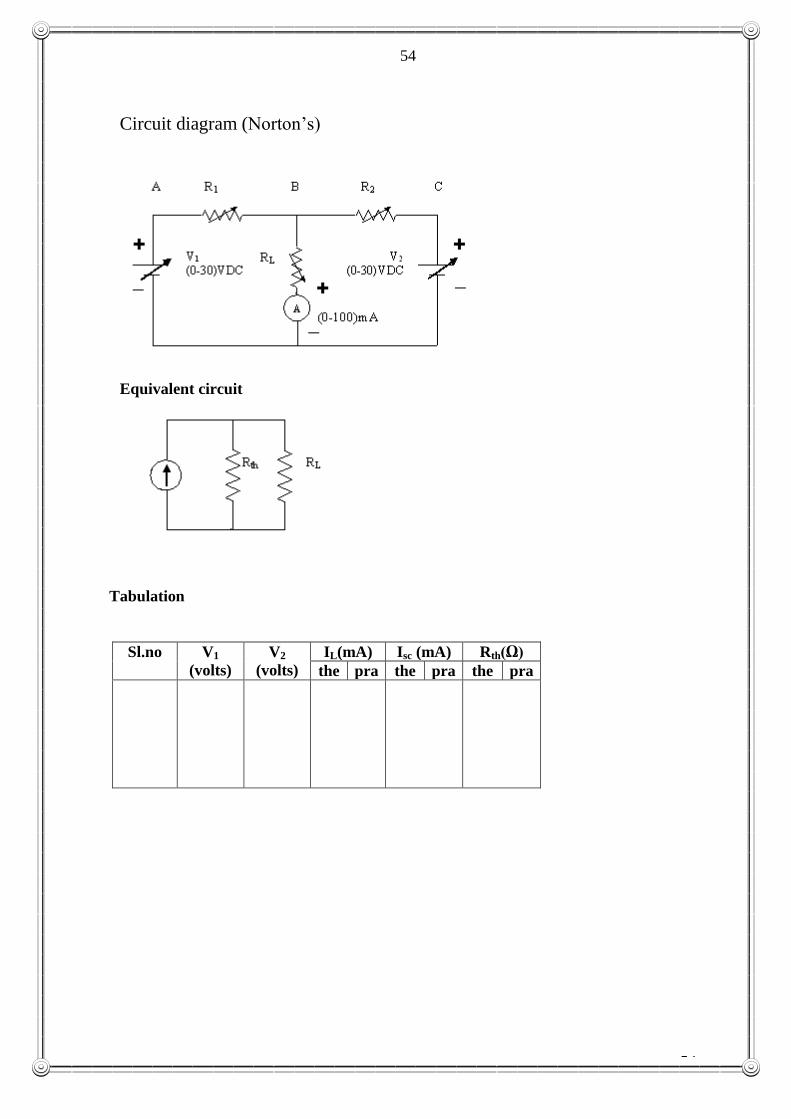
Circuit diagram (Norton‟s)
Equivalent circuit
Tabulation
Sl.no V1
(volts)
V2
(volts)
IL(mA) Isc (mA) Rth(Ω)
the pra the pra the pra
55
55
Now, this value can be verified to be equal to the one which was measured using
the ammeter.
4. The experiment is repeated for different values of the variable resistance and
also by changing the supply voltage
NORTAN‟S Theorem
Any two terminal linear network consisting of voltage sources and impedances
can be replaced with an equivalent circuit consisting of current source (Isc) in parallel with
an impedance (Rth). The current source (ISC) is the short circuit current and the impedance
(Rth) is the Thevenin‟s resistance. Norton‟s theorem is useful to find the current through a
particular element, in general which may consists of several elements along with the
number of voltage and current sources.
Procedure
1.The circuit connections are given as shown in figure. The variable resistances
are initially adjusted to some suitable values. The supply voltages are adjusted to
some values say V1 and V2. In order to find the Thevenin‟s resistance,(Rth) all the
voltage sources are removed and then the resistance between B&E is measured
using the proper resistance range of the multimeter. This reading gives the value
of Thevenin‟s resistance.
2. The branch BE is shorted through an ammeter and short circuit current Isc is
measured.
3. The value of current flowing through RL is measured using the formula.
Lth
thscL
RR
RII
4. The experiment is repeated for different values of the variable resistance and
also by changing the supply voltage.

56
56

57
57
Result
Comparing the observed values and the theoretical values, we infer that they are
almost equal. Thus both theorems are verified both theoretically and practically
Discussion Questions
1. Prove that Norton‟s theorem is the converse of Thevenin‟s theorem.
2. What are the practical applications of Thevenin‟s theorem?
3. Are these theorems applicable for AC circuits? If so, give the statements.
4. What is the internal resistance of an ideal voltage and ideal current sources?
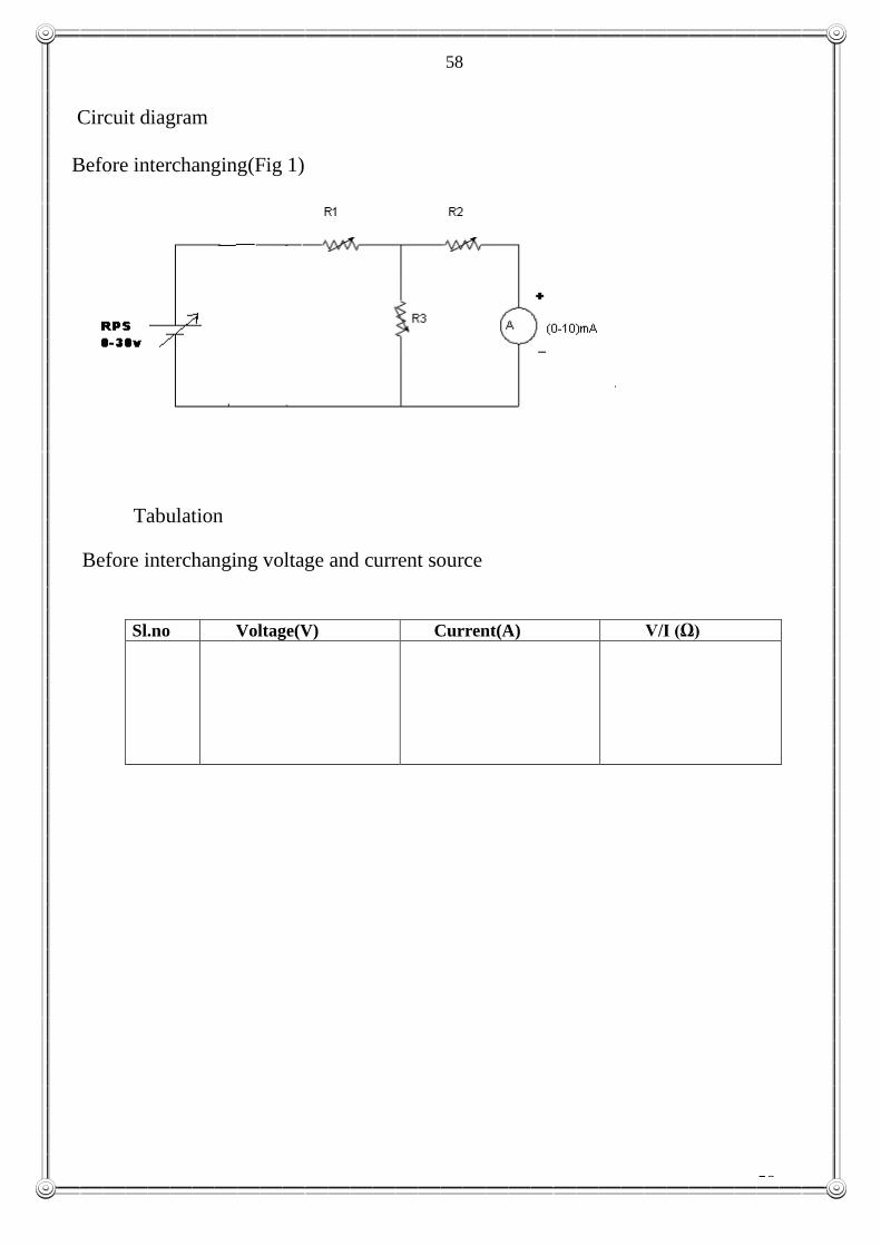
58
58
Circuit diagram
Before interchanging(Fig 1)
Tabulation
Before interchanging voltage and current source
Sl.no Voltage(V) Current(A) V/I (Ω)
59
59
Objective To verify reciprocity theorem experimentally for the given circuit.
References
“Electric Circuit Theory” by Arumugam & Premkumar
“Electric Circuits” by Joseph A. Edminister
“Basic Electricity - A Text Lab Manual” by Paul B. Zbar and Gordon Rockmaker
Knowledge Required
Theorem – statement and their explanation.
Basic circuit laws
Theorem
According to Reciprocity theorem, if we apply some input to a circuit which
consists of resistors, inductors ,capacitors and transformers including coupled circuits, the
ratio of response(o/p) in any element to the input is constant even when the input and
output are interchanged .
Procedure
1. The connections are given as per the circuit diagram as shown in fig.1
2. Switch on the power supply and the rheostat is adjusted to vary the input supply
voltage.
3. For each values of voltage, corresponding current in the short circuited terminal is
noted.
4. The voltage and current sources are interchanged as shown in fig.2.
5. The rheostat is adjusted and the values of current and voltage are noted.
6. The reciprocity theorem was verified by obtaining equal values of ratios of
response to input before and after interchanging the sources.
11. VERIFICATION OF RECIPROCITY
THEOREM

60
60
After interchanging(Fig 2)
After interchanging voltage and current source
Sl.no Voltage(V) Current(A) V/I (Ω)

61
61
Result
Thus the reciprocity theorem was verified both theoretically and practically for the given circuit.
Discussion Questions:
1.What are the practical applications of this theorem?
2. Are this theorem applicable for AC circuits? If so, give the statements
****************************************************
62
62
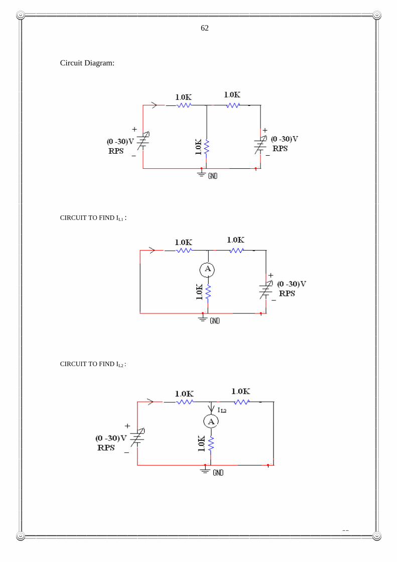
Circuit Diagram:
CIRCUIT TO FIND IL1 :
CIRCUIT TO FIND IL2 :
63
63
Objective To verify superposition theorem experimentally using DC network.
References
“Electric Circuit Theory” by Arumugam & Premkumar
“Electric Circuits” by Joseph A. Edminister
“Basic Electricity - A Text Lab Manual” by Paul B. Zbar and Gordon Rockmaker
Knowledge Required
Theorem – statement and their explanation.
Basic circuit laws
Theorem
Superposition theorem states that in a linear network containing several sources,
the overall response at any point in the network equals the sum of, the responses of each
individual source considered separately replacing the other source by their equivalents.
Procedure
1.Theoretically calculate the value of current IL flowing through RL by
including V1 &V2.
2.Theoretically calculate the value of IL(1) by including V1and S.C.V2.
Also find the value of IL(2) by including V2 alone and S.C.V1.
3.The connections are made as per the given circuit.
4.Find the value of IL(1) with V1 alone.
5.Find the value of IL(2) with V2 alone.
6.Verify theoretically & practically that, IL= IL(1) + IL(2)
12 .VERIFICATION OF SUPERPOSITION
THEOREM

64
64
Tabulation
Parameters
Theoretical values(V)
Practical value(V)
V1 acting alone
V2 acting alone
Both are acting
Design:

65
65
Result
From the tabulated results, super position theorem is verified theoretically &
practically.
Discussion Questions
1. At what situation this theorem can be applicable?
2. What do you mean by linear & bilateral networks?
***********************************************
66
66
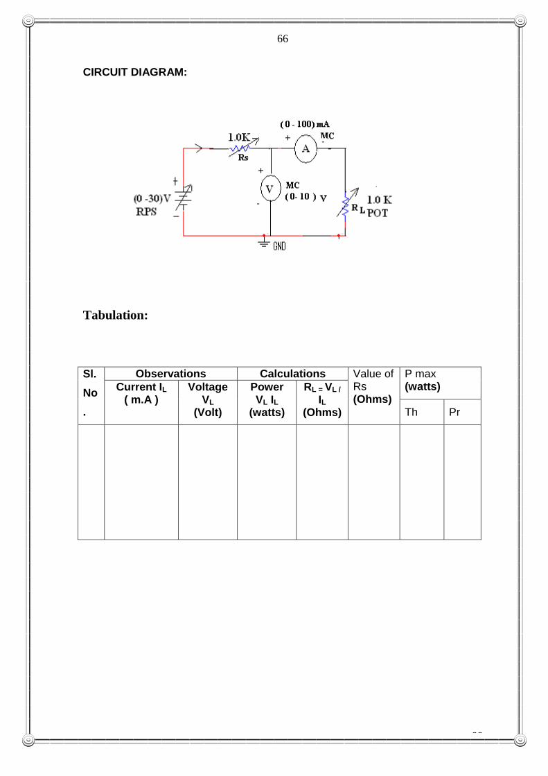
CIRCUIT DIAGRAM:
Tabulation:
Sl.
No
.
Observations Calculations Value of Rs (Ohms)
P max (watts) Current IL
( m.A ) Voltage
VL
(Volt)
Power VL IL
(watts)
RL = VL /
IL
(Ohms) Th Pr
67
67
13. Verification of Maximum Power Transfer theorem
Onjective:
To verify the Maximum Power transfer theorem by conducting suitable test.
REFERENCS:
1).“Engineering circuit Analysis” ,6th
Edition Tata McGraw-Hill publishing
company ltd Author-WH Hayt,J E Kemmerly,S M Durbin
2).“Electrical Engineering Fundamentals”,-Second Edition, Prentice Hall of
India Author-Vincent Del Toro
PROCEDURE:
1. Connections are made as per circuit diagram.
2. Keep the variable point of Rs in a suitable position.
3. Start with maximum resistance adjusted for RL. Note the current through & voltage
across RL.
4. Vary the RL and note the current & voltage. Take a number of readings upto a low
value of RL.
5. Change Rs and repeat steps 3 & 4
6. For every Rs plot RL & power consumed, and find out the value of RL for
maximum power from the graph.
THEORETICAL CALCULATIONS FOR PRESENT CIRCUIT:
Theoretical calculation for circuit diagram 1
The source delivers the maximum power when the load resistance is equal to the source
resistance.
RL= 25Ω
The current I = 50 / (25 + RL ) = 50 /50 =1A
The maximum power delivered to the load P= I2 RL
=1* 25 = 25W

68
68
FORMULAE USED:
PL= IL2 * RL
PL = Power in the Load resistance (RL) in watts.
IL = Load current in amps.
RESULT:
Maximum Power Transfer Theorem was verified for the given circuit
Discussion Questions:
1. When will a circuit deliver maximum power to the load?
2. State Maximum power transfer theorem.
3. State the formula for maximum power delivered to the load?
69
69
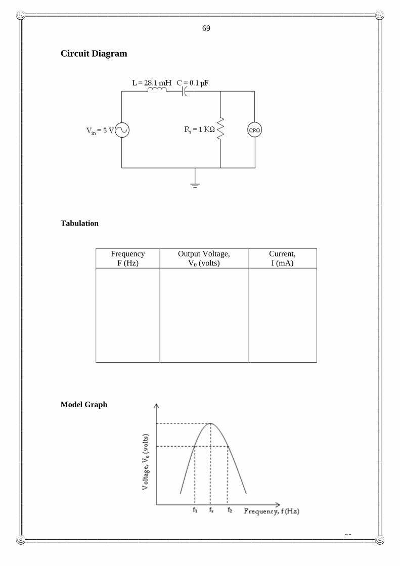
Circuit Diagram
Tabulation
Frequency
F (Hz)
Output Voltage,
V0 (volts)
Current,
I (mA)
Model Graph
70
70
14. Resonant frequency and frequency response of a series RLC Circuit
Objective
To obtain the frequency response characteristic of RLC series circuit.
Reference
1) “Electric Circuit Theory” by Arumugam and Prem Kumaran.
2) “Basic Electricity – A text lab Manual” by Paul B.Zbar and Gordon
Rockmaker
3) “Electricity – Principles and Applications” by Fowler.
Knowledge Required
Series Circuit, resonance, frequency response.
Precautions:
1) Keep the beam intensity down to the minimum required for a particular
setting. Take care to turn down the glare on slow sweep speeds.
2) While making measurements, it should be ensured that time base and vertical
amplifier control are in their calibrated positions.
3) Ensure that the vertical gain control is set above the voltage of the signal to be
measured.
Procedure
Set up inductance value in the DIB using an LCR meter. Connect resistor R, DIB
and capacitor C in series with a signal generator. Adjust the signal generator such that
five volt peak magnitude is achieved on the CRO. Vary the frequency from 100Hz to
100kHz and note down the corresponding voltage across R with the help of the CRO.
Formula used
At resonance, XC = XL
where
1
2C
r
Xf C
2L rX f L
1
2rf
LC
71
71
Result
Thus the frequency response characteristic of RLC series circuit is drawn.
Discussion Questions
1. What is resonance in ac circuits?
2. Write the formula for resonant frequency in RLC series circuit?
3. What are half power frequencies?
4. Define Q factor of a circuit.
5. Prove that resonant frequency is the geometric mean of half power
frequencies.
72
72
Circuit Diagram
Tabulation
Frequency
F (Hz)
Output Voltage,
V0 (volts)
Current,
I (mA)
Model Graph
73
73
15. Frequency response of a Parallel Resonant Circuit
Objective
To obtain the frequency response characteristic of. Parallel Resonant Circuit
Reference “Principles of Electrical Engineering and Electronics” by V.K.Mehta.
Knowledge Required:
Resonant frequency of a parallel circuit
Frequency Response curve
Precautions:
1. Keep the beam intensity down to the minimum required for a particular setting.
2.Take care to turn down the glare on slow sweep speeds.
3.While making measurements, it should be ensured that time base and vertical
amplifier control are in their calibrated positions.
4.Ensure that the vertical gain control is set above the voltage of the signal to be
measured.
Procedure
1. Make the connections as shown in the circuit diagram.
2. Turn on the signal generator and the CRO and increase the output voltage of the
signal generator to 10 volts.
3. Maintain this voltage throughout the experiment and adjust if necessary.
4. Vary the Generator frequency above and below the resonant frequency in a wide
range and measure the current through the multimeter.
5. Calculate the impedance of the circuit at each frequency and record it in a tabular
column.
6. Plot the frequency vs current and frequency vs impedance curves on a semi-log
graph sheet and indicate the resonant frequency.
Result
Thus the frequency response characteristic of Parallel Resonant circuit is drawn.
Discussion Questions
1. What is the condition for parallel resonance?
2. Explain the effects of changes in frequency on the impedance of a parallel RLC
circuit.
3. Explain the effects of changes in frequency on the total current of a parallel RLC
circuit.
4. Compare series and parallel resonant circuit and
5. Define Q-factor in a parallel resonant circuit.
74
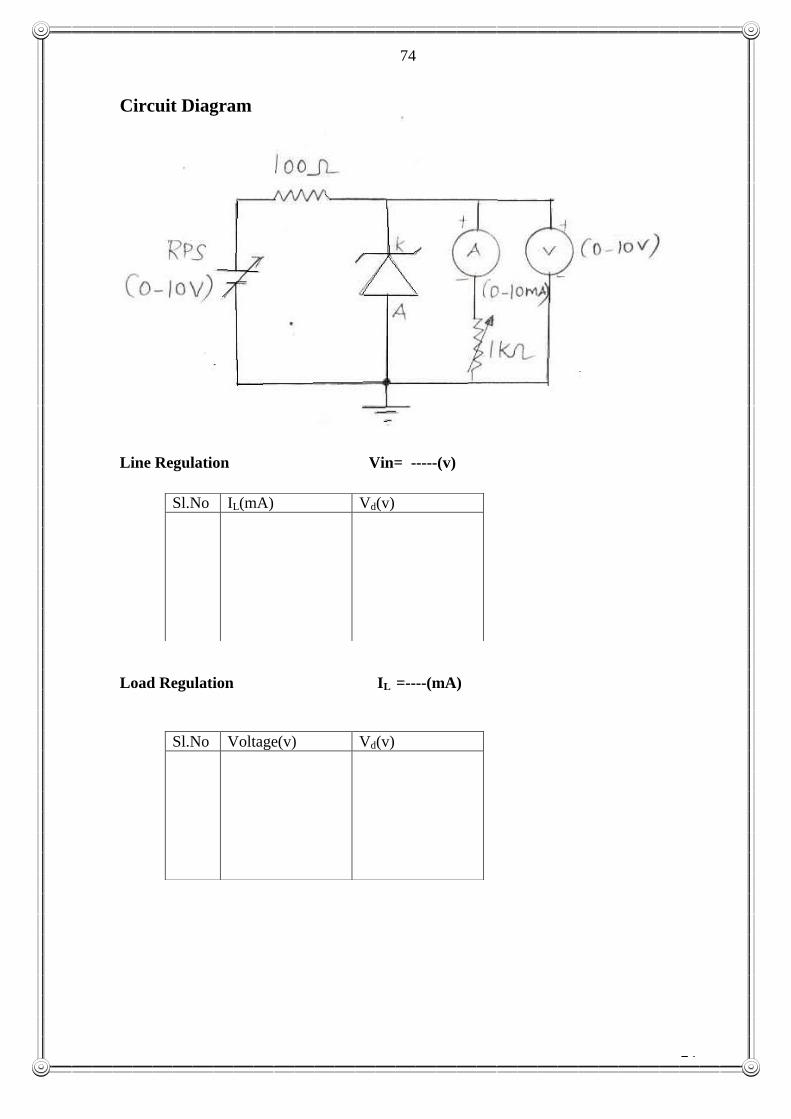
74
Circuit Diagram
Line Regulation Vin= -----(v)
Load Regulation IL =----(mA)
Sl.No IL(mA) Vd(v)
Sl.No Voltage(v) Vd(v)
75
75
Objective
To regulate the output voltage using Zener diode.
Theory
The key feature of a zener diode remain that it maintains reverse voltage across its
terminals constant. So it is used in voltage regulators. There are two ways: 1) Zener
diode as a voltage regulator with a input voltage (line regulation)
2) Zener diode as a voltage regulator with a changing load (Load regulation).
Procedure
1.Connect the circuit as shown in figure.
2.Line regulation :
Vary the input voltage slowly in steps and note down input voltage, output voltage
and ammeter readings corresponding to each setting. Take care that the maximum
current rating is not exceeded. Here the load current IL is maintained constant.
3.Plot a graph between input voltage and diode voltage
4.Load regulation: Vary the values of load current by adjusting the load
resistance and measure the diode voltage. Here input voltage is maintained
constant.
5.Plot a graph between load current and diode voltage.
Result
Thus the line &load regulation were checked using Zener diode.
16. Zener Diode as voltage Regulator