comparison of three smart camera architectures for real-time
TRANSCRIPT

http://www.diva-portal.org
This is the published version of a paper published in International Journal of Advanced Robotic Systems.
Citation for the original published paper (version of record):
Abdul Waheed, M., Thörnberg, B., Palaniappan, P. (2013)
Comparison of Three Smart Camera Architectures for Real-time Machine Vision Systems.
International Journal of Advanced Robotic Systems, 10: Art. no. 402
http://dx.doi.org/10.5772/57135
Access to the published version may require subscription.
N.B. When citing this work, cite the original published paper.
Permanent link to this version:http://urn.kb.se/resolve?urn=urn:nbn:se:miun:diva-19953

International Journal of Advanced Robotic Systems
Comparison of Three Smart Camera Architectures for Real-Time Machine Vision System Regular Paper
Abdul Waheed Malik1,*, Benny Thörnberg2 and Prasanna Kumar2
1 Department of Electronics Design, MidSweden University, Sudsvall, Sweden 2 MidSweden University, Sweden * Corresponding author E-mail: [email protected]
Received 02 Jul 2013; Accepted 20 Sep 2013 DOI: 10.5772/57135 © 2013 Malik et al.; licensee InTech. This is an open access article distributed under the terms of the Creative Commons Attribution License (http://creativecommons.org/licenses/by/3.0), which permits unrestricted use, distribution, and reproduction in any medium, provided the original work is properly cited.
Abstract This paper presents a machine vision system for real-time computation of distance and angle of a camera from a set of reference points located on a target board. Three different smart camera architectures were explored to compare performance parameters such as power consumption, frame speed and latency. Architecture 1 consists of hardware machine vision modules modeled at Register Transfer (RT) level and a soft-core processor on a single FPGA chip. Architecture 2 is commercially available software based smart camera, Matrox Iris GT. Architecture 3 is a two-chip solution composed of hardware machine vision modules on FPGA and an external micro-controller. Results from a performance comparison show that Architecture 2 has higher latency and consumes much more power than Architecture 1 and 3. However, Architecture 2 benefits from an easy programming model. Smart camera system with FPGA and external microcontroller has lower latency and consumes less power as compared to single FPGA chip having hardware modules and soft-core processor.
Keywords Machine Vision, Component Labeling, Smart Camera
1. Introduction
Smart cameras are real-time machine vision systems. Real-time machine vision systems generally perform image capturing, processing of captured images and extracting the useful information which is used for decision making. The typical applications in which smart cameras are applied include process control, surveillance, optical navigation and robot vision. Among these applications, optical navigation and robot vision require high frame speed and low computational latency. This requirement on high frame speed comes from the control and regulation of a robot’s motion [2]. Power consumption must in some cases still be low enough to enable small sized portable and battery operated devices [4]. In addition, most of the above discussed smart camera applications require programmability for easy prototyping and incorporation of future modifications.
1Abdul Waheed Malik, Benny Thörnberg and Prasanna Kumar: Comparison of Three Smart Camera Architectures for Real-Time Machine Vision System
www.intechopen.com
ARTICLE
www.intechopen.com Int. j. adv. robot. syst., 2013, Vol. 10, 402:2013

Pixels
FeaturesSegmentation
Low level
Intermediate level
High levelObjects
Preprocessing
Classification
Recognition
Figure 1. Image processing tasks pyramid [1] Image processing operations are generalized in Figure 1. Low level processing tasks include noise removal, distortion compensation, contrast enhancement etc. The Intermediate level processing include segmentation, labeling and feature extraction. During segmentation, image components and background are separated. Labeling assigns a unique label to each image component. After image component features are extracted, we can classify them into pre-defined classes such that the objects are distinguished. High level processing include object recognition. The data intensity decreases as we move from preprocessing to object recognition. The architecture for real-time image processing should be able to handle low level data intensive pixel processing as well as highlevel mathematical functions. This work is focused on comparison of three smart camera architectures shown in Figure 2. Architecture 1 consists of Machine Vision Modules (MVM) and soft-core processor. MVM contains image capturing, segmentation, labeling and feature extraction. MVM were modeled at RT level. Extracted features are sent to a soft-core processor, MicroBlaze, for the calculation of the camera distance and angle with respect to reference points located on a target board. A soft-core processor is an RT level model of a micro-processor, captured using a Hardware Description Language (HDL) such as VHDL. This RT model is flexible and can be modified based on requirements for a particular application. The HDL description can then be synthesized either for an FPGA or an ASIC. Architecture 2 is commercially available software based smart camera. This smart camera has General Purpose Processor (GPP), on chip RAM, installed windows environment and image processing library. Architecture 3 is similar to Architecture 1, except that the soft-core processor is replaced by an external 32 bit
microcontroller, Atmel AVR32. The application chosen for the comparison of performance metrics is sensing of angle and distance of a camera with respect to a target board. Smart cameras are common in production lines, security applications and for industrial process monitoring. The faster production lines need machine vision system with short response time. Time-critical smart applications such as video based driving assistance, high speed visual feedback for robotic arm [2] and traffic flow control [3] need quick response times. Thus, the processing architecture for these time-critical applications should have high data throughput and low latency. Battery operated smart camera applications demand low power consumption. Smart camera applications such as camera based navigation aid for visually impaired persons [4], [5] smart camera node for video surveillance [6], [7] and information collection from a natural disaster by smart camera [9] require low power consumption for longer battery life time. Low power consumption is also necessary for smart camera nodes that are powered by alternate energy sources such as solar power [8]. Thus, high frame speed and low power consumption are major issues that will be considered when comparing the three presented architectures. The motivation for this study is to gain knowledge about how to choose architecture for a smart camera. High abstraction level programming model and well developed image processing library make commercially available smart camera systems an attractive choice for machine vision application development. On the other hand, an FPGA based system with hardware-software co-design can exploit the potential parallelism present in data intensive image processing applications. Hardware-software co-design requires efficient partitioning of image processing tasks between hardware and software to optimize speed and power consumption. The results from using a single FPGA chip for processing is also compared with a heterogeneous platform using separate chips for FPGA and microcontroller. The results from this comparison can be analyzed to select an architecture based on latency, frame speed, power consumption, ease of programming and level of system integration.
Figure 2. Smart camera architectures
2 Int. j. adv. robot. syst., 2013, Vol. 10, 402:2013 www.intechopen.com

a)
Binary pixel stream input
O/E
En
Data table A
Data table B
Data table
P7 P8 P9 P6
Labeller
Equivalence table
O/E A B EW
En En
Table A Table B
Mux
Resolver
Eq. read port
Gray scale- or colour pixel stream input
Codes
Equivalences
COG calculation
COG data of labelled objects
Table ready
En
b)
c)
Figure 3. Pixel neighborhood, b) Hardware architecture for component labeling and feature calculation, c) Flow graph for software system An alternative technology to realize high throughput and low power smart camera system is by using Application Specific Integrated Circuits (ASIC). ASIC data paths are highly optimized and have low latency. However smart camera application presented in [2-8] require programmability for adaption to the environmental conditions where they are installed and also for incorporation of future modifications to algorithms. High Non Recurring Engineering (NRE) costs for ASIC Application development make it difficult to easily incorporate changes. This constraint makes the FPGA platform more suitable than ASIC for smart camera applications where programmability is required. The main scientific contribution of this work is the performance evaluation of three different architectures for a smart camera. The chosen architectures have their own characteristic, and this performance evaluation give the smart camera designer guidance about the choice of specific architecture based on application and performance requirement.
2. Related Work
Smart camera platforms have capabilities of image- capturing and processing to obtain the desired information from images [10], [11]. After processing of the captured images, the obtained results can be sent via
some communication channel to a base station or some critical decision can be taken locally at smart camera node. A multimedia processor is one of the options to implement a smart camera system. The Trimedia processor series is developed by Phillips. Trimedia TM3270 is Very Long Instruction Word (VLIW) based architecture [13]. This processor can support up to 7 billon operations per second. Applications can be developed using C language. The dynamic power consumption of this processor is around 1 mW/MHz. The processor can be operated at maximum 450 MHz. There are also other similar multimedia processors available e.g. SH series from Hitachi, Itanium2 developed by Intel and Hewlett-Packard. Commercially available software based smart cameras have both an image sensor and an on-board programmable processing platform. Matrox Iris GT [14], NI-1772 from National Instruments [15] or XCISX100C from SONY[16] have reasonable high processing capabilities. Due to the installed operating system and the imperative programming model, the designer’s work to develop applications are made simpler compared to RTL-modellling. However, the power consumption of these smart cameras is in tens of watts, which is not realistic for battery operated smart cameras.
3Abdul Waheed Malik, Benny Thörnberg and Prasanna Kumar: Comparison of Three Smart Camera Architectures for Real-Time Machine Vision System
www.intechopen.com

Smart camera platforms can be built from an image sensor and an optimized data path for processing of captured images [17]. FPGAs and custom designed VLSI circuits can be employed to achieve the desired functionality with low power consumption. FPGAs are reprogrammable while VLSI data paths are more optimized and consume very low power. Re-programmability in an FPGA based platform, massive parallelism and shorter design times than VLSI circuits make them suitable for smart camera applications. High throughput and low power consumption are fundamental requirement for many smart camera applications. A smart camera used in feedback loop of a robotic arm to re-grasp an object is presented by Noriastu et al [2]. This vision system provides feedback at a rate of 1 KHz so that the robotic arm and finger can adjust their position according to the object’s position. Industrial surface monitoring of cylindrical objects and sheets is presented by Tomohira et al [12]. Camera based inspection of rapidly spinning object and fast moving sheet needs high throughput to be able to inspect any defects on the surface. Battery operated smart camera applications demand low power consumption to achieve a reasonable battery life time. The application such as vision based navigation support for blind people is presented by Joao et al [4]. Stereovision cameras were attached on chest of a blind person and captured image were sent to a portable computer for detection of obstacles and planning of path. Battery operated smart camera systems with low power consumption is suitable for this scenario to reduce the size and easy mounting together with image sensors. The surveillance applications presented in [5-7] are also battery powered camera based system that requires low power consumption. Wu Liming et al presented experiments on image processing tasks executed on a single chip using a soft-core processor MicroBlaze. They aimed to compare the performance of a software implementation with a software/hardware implementation. Bitonic sort and median filter were used as test cases for the evaluation of system performance. They concluded that a system design using soft-core processor with hardware IPs not only speeds up the development time but also results in a more than ten times performance improvement as compared to that of a software implementation [19].
Figure 4. On chip system architecture1
p
ØØ
Dqp
ß
Dwq
DpzDwz
Dxyx
yf
qw
Dqz
z
Figure 5. Triangulation view A summary of different smart camera architectures and platforms was discussed by Shi Y et al [20]. The selection of architecture depends on the application. For in-camera processing of captured images, homogenous and heterogeneous platforms are described. In most smart camera applications, there are data intensive tasks like segmentation, component labeling, feature extraction and math intensive tasks such as pattern matching. Authors suggested that data intensive tasks should be implemented on parallel architectures, while control and mathematical computations can be performed using a Application RISC or DSP processor. One such smart camera system for face recognition is presented by Broeres et al [21]. The main contribution of this article is an evaluation of three different smart camera systems having computation either: on a single-chip FPGA, or a heterogeneous system consisting of an FPGA and microcontroller versus a commercially available smart camera based on an Intel computer and Microsoft Windows. From the study of related literature we have not found any comparison of this nature. Therefore this study is a valuable scientific contribution that will help a smart camera designer about choice of particular architecture. The remaining section of this paper is organized as follows:. Section 3 explains the different architectures used for comparison. Section 4 describes experimental setup and methodology, Section 5 explains results, and Section 6 deals with discussion on the results.
3. Proposed architectures
In this section we will discuss the proposed architectures.
3.1 Proposed Architecture 1
Architecture 1 consists of three major components i.e. MVMs, soft-core processor MicroBlaze and software system. A CMOS image sensor (MT9V032) from Micron, operating at maximum clock frequency of 27 MHz, was used to capture the images. The VmodBB connector from Digilent is used to connect camera signal to Spartan-6 development board. This is a parallel interface
4 Int. j. adv. robot. syst., 2013, Vol. 10, 402:2013 www.intechopen.com

transferring one pixel per clock cycle. The capture images are fed to MVMs for further processing. MVMs perform image capturing, segmentation, labeling and feature extraction. The features were sent to the soft-core processor. Computation of distance and angle was done by a software system executed on the processor. In past, FPGAs used to be homogeneous hardware platforms containing a huge set of logic blocks. Today’s FPGA architectures are more of heterogeneous computational platforms. FPGAs still have a large set of configurable logic gates but they have also embedded arithmetic units, block memories and memory controllers. In addition, the FPGA circuit technologies are targeted towards very low power applications.
3.1.1 Machine Vision Modules
MVMs were modeled at RT level using the hardware descriptive language VHDL. Images captured by an image sensor are processed at a segmentation step. Segmentation in this case involves a simple thresholding of gray levels to separate bright reference points from their background. The segmented images are further separated into background and a set of labeled image components while at the same time, features are extracted for each component. The hardware architecture for image component labeling and feature extraction is shown in Figure 3(b). For the labeling process of a typical image, the neighborhood is shown in Figure 3(a). The pixel P5 is assigned a label based on its neighboring pixels P6 to P9. A delay line of one FIFO-buffer and two registers hold the labels assigned to previous row [23]. The kernel for labeling and feature extraction is depicted Figure 3(b). The labeler assigns labels to P5 depending on its neighbors. If the labeler does not find any labeled pixels in the neighborhood, a new label is assigned to P5. If the labeler finds two different labels in the
neighborhood of P5, then P5 is assigned to one of these labels and the detected pair of labels must be recorded as equivalent. This is, because all connected pixels must be recognized as belonging to the same image component. The equivalences are recorded in Table A or B based on odd or even frame. Equivalences are resolved after labeling whole frame such that all labels in an image component should have same value. This label assigning and resolution runs in parallel in Table A or B. Along with labeling process we also accumulate data for feature extraction in Data table A or B. When all equivalences are resolved in Table A or B, the Table ready signal is sent to feature extraction unit e.g. COG calculation in Figure 3(b). The extracted features are sent to soft-core processor. The software system then calculates the distance and angle information of camera from reference points.
3.1.2 Soft-Core Processor And Interconnects
A vendor specific system based on a Xilinx Spartan 6 FPGA is shown Figure 4. MicoBlaze is Harvard architecture based 32 bit RISC soft processor. MicroBlaze contains Memory Management Unit, instruction and data cache, floating point unit and configurable pipeline depth. A Processor Local Bus (PLB) is used to communicate between process and different peripherals. Fast Simplex Link (FSL) or Advance eXtensible Interface (AXI) can be used to communicate between MicroBlaze and user defined hardware IP’s. A MicroBlaze [24] soft processor connects to MVM via a Fast Simplex Link (FSL) bus. As a soft-core processor, MicroBlaze is implemented entirely in the general-purpose logic fabric of Xilinx FPGAs. The MicroBlaze based system can be developed under Xilinx's EDK (Embedded Development Kit) environment. FSL is a uni-directional point-to-point FIFO based communication channel bus that is used to perform fast communication between the MVM and the MicroBlaze processor.
Figure 6. Two chip system for architecture 3
Frame Speed/sec Power Consumption Total Architecture 1
77
FPGA Image Sensor 400mW 80mW 320mW
Architecture 2 33 5.5W 5.5W Architecture 3
77
FPGA Micro-controller Image Sensor 368mW 48mW 0.3mW 320mW
Table 1. Results (power consumption)
5Abdul Waheed Malik, Benny Thörnberg and Prasanna Kumar: Comparison of Three Smart Camera Architectures for Real-Time Machine Vision System
www.intechopen.com

Images captured as a continuous stream of video are fed to the MVM. The image component features extracted by the MVM are sent to the Microblaze through the FSL bus. A UART and a Timer were interfaced with the MicroBlaze through a Processor Local Bus (PLB). The UART is used to send computed values for distances and angles to an external host system.
3.1.3 Softwar System
The software system defines the distance and angle measurement of camera from a set of reference points located on a target board The hardware-software partitioning for Architecture 1 and 3 is shown in Figure 3(c). In these two architectures the software System performs the distance and angle measurement of camera from reference points based on extracted Centre of Gravity “COG” values computed by MVM. For Architecture 1 and 3, the software was coded using imperative programming language “C”. The general flow graph of all computational operations is shown in Figure 3(c). The MVM modules compute the “COG” of reference points as a required feature. The distance of camera from the reference point was calculated using lens formula [25]. After knowing the distance between camera and reference points, we used triangulation to calculate the viewing angle of camera. Image processing tasks are divided between MVM and software system such that all data intensive task are modeled at RT level. Only features data is sent from MVM to software system that will reduce communication overhead associated with data transfer from MVM to software system. Different strategies for partitioning image processing tasks between hardware and software are studied in [22]. The result in this literature shows that minimum data transfer between hardware modules and software can be achieved if data intensive image processing tasks up to feature extraction, as shown in Figure 1, are performed on hardware modules. Thus, the partitioning between hardware and software is based on data intensity. The RT level design models the synchronous data flow of signals in digital circuits. RT level is motivated when we have synchronous data intensive system e.g. pixel stream from a camera. However, non data intensive but more reactive and control flow intensive computations can be well performed by micro-controller. This fact is also highlighted in [19]. In addition, the implementation of complex mathematical equations in RT level design is time consuming and requires high NRE cost.
3.2 Proposed architecture 2
The second architecture chosen for comparison is a commercially available smart camera, Matrox Iris GT. This smart camera comes with Microsoft Windows XP embedded as operating system. Developing a vision
application in C++ is much easier compared to RTL modeling for the other two architectures. Iris GT has a Sony ICX274AQ progressive scan CCD image sensor having square pixels of diagonal size 8.923mm. It has an onboard 1.6GHz Intel atom processor with 512MB of volatile and 2GB of non volatile memory. Matrox Iris smart camera contains Intel® Atom® (Z530) embedded processor. The Intel atom (Z530) is 32 bit processor. This processor is common in many note books and embedded applications. This processor has 512KB of cache and Front Side Bus (FSB) that operates at 533 MHz. The processor support Hyper- Threading and operate at 1.6GHz clock frequency It has three main interfaces such as digital I/O, VGA/USB and 100/1G Ethernet. The flow graph for Architecture 2 is same as presented in Figure 3(c). All tasks from image capturing to distance and angle of camera, computational steps 1 to 8 in Figure 3(c) are executed on software system for Architecture 2. The Matrox Imaging Library (MIL) helps easy prototyping and contains most of basic image processing functions that reduce the workload on developer. The developer of applications uses the high level programming model VisualC++.
3.3 Proposed architecture 3
Architecture3 is similar to Architecture1 except that the soft-core processor is replaced by an Atmel AVR 32 bit micro-controller AT32UC3B0256 [26] as shown in Figure 6. This micro-controller has high processing capabilities and has low power consumption. AT32UC3B0256 has six different operation modes in order to meet different performance and power consumption requirement. The maximum clock frequency can be 60 MHz. Architecture 3 includes 32 bit micro-controller Atmel AVR 32 AT32UC3B0256 to execute software system. Atmel AVR 32 is RISC base micro-controller. The controller can be clocked up to 60 MHz. The micro-controller provides 6 different power modes that can be adopted to optimize power consumption depending upon the performance requirement of application. To measure the performance and power consumption we used SENTIO32 [27] board developed at Mid-Sweden University, Sweden. The SENTIO32 board is equipped with an AVR microcontroller and communication interfaces. The extracted features from MVM were transferred to the microcontroller board using SPI link operating at a clock frequency of 8 MHz. The software system for Architecture 3 is already explained in section 3.1.3.
3.4 Viewing Angle and Distance Calculation
For all three architectures, computation of distance and angle from camera to a target board is defined by
6 Int. j. adv. robot. syst., 2013, Vol. 10, 402:2013 www.intechopen.com

software. This section describes the mathematical formulas captured in software in accordance with computational step 4 to 7 as shown in Figure 3(c). Inputs for the computation are the COG values of reference points, focal length of camera, computed distances between reference points in image plane and known distances between reference points on the target board. The camera was placed in front of target board in a way to achieve the orthogonal projection on camera lens. The line, Dwq, in Figure 5, show the alignment of the target board. We are interested in find the reference points to camera distance Dwz and view angle Ф. Viewing angle of camera from target board was calculated by solving similar triangles, ∆pqz and ∆xyz. Following information is used to draw the final equation for distance and angle of camera. Dwz Distance between the camera and Black board ф Viewing angle of the camera Dwq Euclidean distance between points on the board Dxy Euclidean distance between points in image plane f Focal length of the camera Dqz Distance between the focal point(z) and reference
point(q) on board as shown in Figure 5 Dpz Distance between the focal point(z) and projection
of reference point(w) as shown in Figure 5 ∠zxy = ∠wpq = 90degree, ∠pwq = ф= viewing angle,
∠pqw = β
(1)
(2)
4. Experimental setup and methodology
The experimental setup used for Architecture 1 is shown in Figure 7(a). It consists of white reference points fixed on a black colored target board. A CMOS image sensor was clamped on a stand along with lightning facilities. The image sensor captures images and sends them to an experimental FPGA board, which executes the embedded real-time machine vision system described in section 3. Computed distance and angle are sent from the FPGA board using RS232 to a host computer. This experiment is performed to make a functional verification of the system for a few selected distances and angles. The Atlys Spartan6 board has the capacity of monitoring power consumption on different voltage rails available on Digilent board. The FPGA core is connected to a 1.2 Volt rail. The monitors are based on Linear Technology’s LTC2481C sigma-delta analog-to-digital converters that return 16-bit samples for each channel. The latency of the soft-core processor is measured by code profiling i.e. using a timer at start and end of program. The latency
value is also verified using a logic analyzer. Specific pattern is sent to a set of IO pins at start and end of software program allowing for the logic analyzer to trigger and compute the time difference between the two patterns. The latency of MVM modules are computed in simulations and also measured using a logic analyzer. These latency values contain camera overhead for row and frame synchronization. For experiments with Architecture 2, the Matrox IRIS GT smart camera is placed in front of the reference board. Images are continuously grabbed and processed from a stream of video generated at the image detector output. The smart camera is configured to simultaneously grab next image and process current image in an interleaved mode. A host computer is needed for development of applications. Camera and host computer are connected using a 1Gbit Ethernet interface configured to a static IP address. The application is developed in Microsoft visual studio using Matrox imaging library and deployed in the Iris GT using a remote debugger. The programming language used to develop applications is visual C++. When the application is deployed in Iris GT, it can solely run without any connection to the host computer. The camera is programmed to execute image processing steps like segmentation, component labeling and feature extraction. Firstly, during segmentation, the white reference points are separated from the image background. Later at component labeling and feature extraction, all reference points are labeled into unique image objects and their COG values are computed as object features. Euclidean distances between reference points are calculated based on their COG values. Distance and angle are computed in accordance with equations (1) and (2). The computed values of distance and angle are then transmitted using a serial cable to a host computer and viewed on a graphical display using LabVIEW software environment, as shown in Figure 7(b). Iris GT computes and transmits distance and angle for every frame such that the actual camera position is updated on the LabVIEW graphical display at a rate of 33values per second. The latency for the smart camera is measured using code profiling. Power measurement for smart camera is made using voltage- and ampere meters connected to the camera through a break out board [14] .
(3)
Experimental setup for Architecture 3 is similar to Architecture 1 except that the soft-core processor is replaced with a microcontroller assembled on a second circuit board. The extracted features from MVM are sent to the microcontroller through SPI for further
7Abdul Waheed Malik, Benny Thörnberg and Prasanna Kumar: Comparison of Three Smart Camera Architectures for Real-Time Machine Vision System
www.intechopen.com
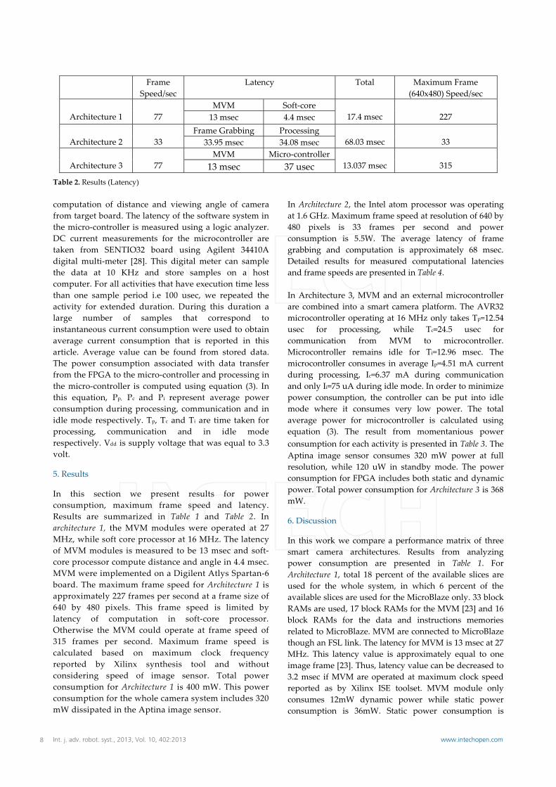
Frame Speed/sec
Latency Total Maximum Frame (640x480) Speed/sec
Architecture 1
77
MVM Soft-core 17.4 msec
227 13 msec 4.4 msec
Architecture 2
33
Frame Grabbing Processing 68.03 msec
33 33.95 msec 34.08 msec
Architecture 3
77
MVM Micro-controller 13.037 msec
315 13 msec 37 usec
Table 2. Results (Latency) computation of distance and viewing angle of camera from target board. The latency of the software system in the micro-controller is measured using a logic analyzer. DC current measurements for the microcontroller are taken from SENTIO32 board using Agilent 34410A digital multi-meter [28]. This digital meter can sample the data at 10 KHz and store samples on a host computer. For all activities that have execution time less than one sample period i.e 100 usec, we repeated the activity for extended duration. During this duration a large number of samples that correspond to instantaneous current consumption were used to obtain average current consumption that is reported in this article. Average value can be found from stored data. The power consumption associated with data transfer from the FPGA to the micro-controller and processing in the micro-controller is computed using equation (3). In this equation, Pp, Pc and Pi represent average power consumption during processing, communication and in idle mode respectively. Tp, Tc and Ti are time taken for processing, communication and in idle mode respectively. Vdd is supply voltage that was equal to 3.3 volt.
5. Results
In this section we present results for power consumption, maximum frame speed and latency. Results are summarized in Table 1 and Table 2. In architecture 1, the MVM modules were operated at 27 MHz, while soft core processor at 16 MHz. The latency of MVM modules is measured to be 13 msec and soft-core processor compute distance and angle in 4.4 msec. MVM were implemented on a Digilent Atlys Spartan-6 board. The maximum frame speed for Architecture 1 is approximately 227 frames per second at a frame size of 640 by 480 pixels. This frame speed is limited by latency of computation in soft-core processor. Otherwise the MVM could operate at frame speed of 315 frames per second. Maximum frame speed is calculated based on maximum clock frequency reported by Xilinx synthesis tool and without considering speed of image sensor. Total power consumption for Architecture 1 is 400 mW. This power consumption for the whole camera system includes 320 mW dissipated in the Aptina image sensor.
In Architecture 2, the Intel atom processor was operating at 1.6 GHz. Maximum frame speed at resolution of 640 by 480 pixels is 33 frames per second and power consumption is 5.5W. The average latency of frame grabbing and computation is approximately 68 msec. Detailed results for measured computational latencies and frame speeds are presented in Table 4. In Architecture 3, MVM and an external microcontroller are combined into a smart camera platform. The AVR32 microcontroller operating at 16 MHz only takes Tp=12.54 usec for processing, while Tc=24.5 usec for communication from MVM to microcontroller. Microcontroller remains idle for Ti=12.96 msec. The microcontroller consumes in average Ip=4.51 mA current during processing, Ic=6.37 mA during communication and only Ii=75 uA during idle mode. In order to minimize power consumption, the controller can be put into idle mode where it consumes very low power. The total average power for microcontroller is calculated using equation (3). The result from momentanious power consumption for each activity is presented in Table 3. The Aptina image sensor consumes 320 mW power at full resolution, while 120 uW in standby mode. The power consumption for FPGA includes both static and dynamic power. Total power consumption for Architecture 3 is 368 mW.
6. Discussion
In this work we compare a performance matrix of three smart camera architectures. Results from analyzing power consumption are presented in Table 1. For Architecture 1, total 18 percent of the available slices are used for the whole system, in which 6 percent of the available slices are used for the MicroBlaze only. 33 block RAMs are used, 17 block RAMs for the MVM [23] and 16 block RAMs for the data and instructions memories related to MicroBlaze. MVM are connected to MicroBlaze though an FSL link. The latency for MVM is 13 msec at 27 MHz. This latency value is approximately equal to one image frame [23]. Thus, latency value can be decreased to 3.2 msec if MVM are operated at maximum clock speed reported as by Xilinx ISE toolset. MVM module only consumes 12mW dynamic power while static power consumption is 36mW. Static power consumption is
8 Int. j. adv. robot. syst., 2013, Vol. 10, 402:2013 www.intechopen.com

dominant due to low device utilization as compared to total logic cells available on spartan6 LX45. Smaller FPGAs such as spatran6 LX25 or spatran6 LX16 can be selected to reduce static power. Results clearly show that the Architecture1 and 3 have lower latency and are more power efficient than Architecture2. The Microsoft Windows based smart camera have ease of application development as its application development environment is supported by an image processing library to choose among different functions. This ease of programming model comes at the cost of higher power consumption and larger latency compared to the other two architectures. The results in Table 4 show that Matrox smart camera misses some of the frames while continuously grabbing and processing a video stream. These missed frames come as a result of higher average processing time than compared to the time needed for frame grabbing. Hence, a homogeneous sampling in time domain cannot be guaranteed. On the other hand, the FPGA based systems we have proposed can process a new pixel at each clock cycle, thus greatly reducing the risk that frames are missed. MVM modules with soft-core processor provide a one-chip solution. A soft-core processor also has the benefit that it is very flexible such that a designer can add different modules of their own choice, but the soft processor’s data paths are not as optimized as compared to the Atmel micro-controller used for Architecture 3. The latency of program in soft-core processor can be reduced by increasing the clock frequency but it will subsequently increase the power consumption. The results in Table 2 clearly show that latency of software system when executed on an external micro-controller is much less as compared to soft-core processor. As the execution in microcontroller is a few microseconds, we can force the micro-controller into sleep mode to further reduce the power consumption. One obvious benefit from using a smart camera based on Intel computer and Microsoft Windows is the rapid design times. Application programming is done using a high abstraction level language if compared to Architecture 1 and 3 which partly need modeling of hardware system at RT-level. RT-level modeling means
that all computations and data transactions on register level needs to be scheduled for each clock cycle. A library of hardware IP-components could ease this complex programming model. The workload for the microprocessors in both Architecture 1 and 3 as well as for the Intel computer in Architecture 2 is for the general applications data dependent. The more image components in a single image, the more features to process per time unit. Efficient segmentation of images is required to segregate objects of interest from image background, so that minimum number of unwanted objects left after segmentation process. The latency time reported in Table 2 for MVM is valid for a frame speed of 77 frames per second (fps). This frame speed can easily drop for Architecture 1 if number of image components after segmentation increases. This is because the latency for computation in microprocessor will risk of becoming larger than the frame period resulting in lost frames. Architecture 3 is much more tolerant for increase in number of image components. If the reported latency of 37 us for computation in the microprocessor and for six image objects is linearly extrapolated, it will require more than two thousand objects per image before the frame speed in Architecture 3 starts to drop from the input image sensor speed of 77 fps The maximum frame speed for the MVM on FPGA is estimated from the maximum clock frequency reported by the design tool set. This maximum speed will be almost independent of number of image components due to a high level of data parallelism and a mostly synchronous data flow. Table 2, rightmost column reports the maximum frame speed for the video processing without considering speed of image sensor. The maximum frame speed of image sensor MT9V032 is quite low as compared to achieved frame speed presented in Table 2. If we want to operate the system at maximum speed as reported in Table 2, we need another image sensor providing much higher bandwidth on the output video stream.CMV2000 from CMOSIS is an example of a CMOS sensor that can operate at maximum 340 fps at 2 Mega pixel resolutions.
Activity Momentanious Current Time Consumed Applied Voltage Momentanious Power Consumption
Processing 4.54 mA 12.54 usec 3.3 v 14.88 mW Communication 6.37 mA 24.5 usec 3.3 v 21.02 mW
Idle 75 uA 12.96 msec 3.3 v 0.24 mW Overall mean power consumption for micro-controller in Architecture3 is 0.3mW
Table 3. Results (power consumption of each activity run on Micro-controller in Architecture 3)
9Abdul Waheed Malik, Benny Thörnberg and Prasanna Kumar: Comparison of Three Smart Camera Architectures for Real-Time Machine Vision System
www.intechopen.com

S No Processed frames
Missed frames
Computational time in sec
Frame rate per second
Computation latency
Frame Grabbing latency
1 2014 280 68.31 30.18 33.90ms 33.10ms 2 1613 211 54.47 29.43 33.70ms 33.90ms 3 4718 749 161.75 29.40 34.20ms 34.00ms 4 2043 314 70.16 28.53 34.34ms 35.04ms 5 1562 236 53.72 30.38 34.39ms 32.91ms 6 3586 562 122.89 27.19 34.26ms 36.76ms 7 2502 390 85.92 28.65 34.34ms 34.90ms 8 5954 943 203.84 27.80 34.23ms 35.96ms 9 7904 1081 265.32 29.96 33.56ms 33.36ms 10 2547 397 87.43 29.10 34.32ms 34.35ms 11 4713 634 158.19 33.92 33.50ms 29.47ms 12 6014 962 206.18 29.71 34.28ms 33.65ms
Table 4. Results (computational and frame grabbing latency in smart camera)
Figure 7. Experimental setup (a) (b) These results indicate that the maximum frame speed of the whole system is limited by the microprocessor for Architecture 1. If Architecture 1 is run at maximum frame speed of MVM, the risk of missed frames will be high due to that the latency of computation in microprocessor will be closer to the frame period. Consequently, for a general application, it will not be realistic to run Architecture 1 at such high frame speed as the maximum for MVM and without missing frames. The maximum frame speed for Architecture 3 is limited by the hardware MVM. The optimized data paths in the stand-alone Atmel micro-controller are able to run software system much faster as compared to soft-core processor. Thus, a realistic machine vision system at hundreds of fps will require a powerful micro-controller or digital signal processor to run the control flow and mathematical computations. Major FPGA vendors are incorporating hard processor IPs along with programmable logic on single chip. Zynq-7000 [29] from Xilinx and SmartFusion2 [30] from Actel are some recent example of them. Both systems include ARM® Cortex™ processors interfacing with FPGA programmable logic through high speed, low power communication channels. We have not included any of these later and more powerful FPGA families in this study but we aim to investigate their performance in future studies.
We have not considered different choices of image sensors in this study. Our study is focused on choice of architecture for image processing and analysis. However, the Aptina CMOS sensor used in our experimental setup for architecture 1 and 3 represents the major power consumption for those systems.
7. Conclusion
In this work we have compared a performance matrix of three smart camera architectures. This comparison was done for real-time computation of distance and angle of a camera from a set of reference points located on a target board. Architecture 2 is a commercially available smart camera based on an Intel computer and Microsoft Windows. It is power hungry and has longer latency than Architecture 1 and 3. However, this software based platform is attractive due to its use of a high level programming model and a source code library for image processing. Architecture2 should be the first choice when short engineering time is the most important design metric. Further, we have shown that the hardware based smart camera systems presented as Architecture 1 and 3 have better performance in terms of frame speed and latency. In addition, FPGA based systems consume much less power if compared with the Microsoft Windows based smart camera. Architecture 3 is a heterogeneous
10 Int. j. adv. robot. syst., 2013, Vol. 10, 402:2013 www.intechopen.com
solution having FPGA and an external microcontroller. It has both lower latency and lower power consumption than the single-chip soft-core based system design on FPGA. This lower power consumption is due to the more optimized data paths of the Atmel microcontroller if compared with a soft processor on FPGA. In addition, data transfers between FPGA and microcontroller are kept at minimum by a well partitioned algorithm between hardware and software leading to lower overall power consumption for the microcontroller. We recommend using Architecture 3 when speed and power are the most important design metrics. Architecture 1 based on soft-core processor offers more flexibility, portability and higher level of system integration. If portability, small physical sizes and high level of integration are the most important design metrics, we recommend using Architecture 1.
8. References
[1] Donald B. (2011) Design for embedded image processing on FPGA, John Wiley & Sons (Asia) Pte Ltd. pp 7-9.
[2] Furukawa N, Namiki A, Taku S, Ishikawa M. (2006) "Dynamic regrasping using a high-speed multifingered hand and a high-speed vision system" Robotics and Automation, 2006. ICRA 2006. Proceedings 2006 IEEE International Conference on , pp.181,187, 15-19 May 2006
[3] Belbachir, Ahmed Nabil (2009) (Ed.), Smart Cameras, Springer ISBN 978-1-4419-0953-4 pp 48-50
[4] João José, Miguel Farrajota, João M.F. Rodrigues, J.M. Hans du Buf,(2011) “The SmartVision local navigation aid for blind and visually impaired persons” international journal of digital content technology and its application Vol.5 May 2011.
[5] Emina Petrović, Adrian Leu, Danijela Ristić-Durrant and Vlastimir Nikolić. Stereo Vision-Based Human Tracking for Robotic Follower, International Journal of Advanced Robotic Systems, DOI: 10.5772/56124
[6] Marcozzi, D, Conti, M (2007) "Image processing performance analysis for low power wireless image sensors," Intelligent Solutions in Embedded Systems”, 2007 Fifth Workshop on pp.1,12, 21-22 June 2007 doi: 10.1109/WISES.2007.4408503
[7] Rasheed Z, Taylor G, Yu L, Lee, M, Choe T, Guo F, Hakeem A, Ramnath K, Smith M, Kanaujia A, Eubanks D, Haering N.(2010) "Rapidly Deployable Video Analysis Sensor units for wide area surveillance," Computer Vision and Pattern Recognition Workshops (CVPRW), 2010 IEEE Computer Society Conference on pp.41,48, 13-18 June 2010 doi: 10.1109/CVPRW.2010.5543799
[8] Magno M, Brunelli D, Thiele L, Benini L.(2009) "Adaptive power control for solar harvesting multimodal wireless smart camera," Distributed Smart
Cameras, 2009. ICDSC 2009. Third ACM/IEEE International Conference on pp.1,7, Aug. 30 2009-Sept. 2 2009 doi: 10.1109/ICDSC.2009.5289358
[9] Sato H, Kawabata K, Suzuki T, Kaetsu H, Hada Y, Tobe Y.(2008) "Information gathering by wireless camera node with passive pendulum mechanism," Control, Automation and Systems, 2008. ICCAS 2008. International Conference on, pp.137,140, 14-17 Oct. 2008 doi: 10.1109/ ICCAS.2008.4694539
[10] W. Wolf, B. Ozer, and T. Lv. (2002) Smart cameras as embedded systems. Computer, 35(9):48–53, 2002.
[11] M. Bramberger, A. Doblander, A. Maier, B. Rinner, and H. Schwabach (2006). Distributed embedded smart cameras for surveillance applications. Computer, 39(2):68–75, 2006.
[12] Tomohira T, Takashi K, Masatoshi I.(2010) “Surface image synthesis of moving spinning cans using a 1,000-fps area scan camera” Machine vision and Application August 2010, Volume 21, Issue 5, pp 643-652.
[13] J.-W. van de Waerdt et al. (2005)”The TM3270 media-processor. In MICRO 38”: Proceedings of the 38th annual IEEE/ACM International Symposium on Micro architecture, 2005.
[14] http://www.matrox.com/imaging/en/products/smart_cameras/iris_gt/ last accessed (2013).
[15] http://sine.ni.com/nips/cds/view/p/lang/en/nid/210029#specifications last accessed (2013).
[16] http://pro.sony.com/bbsc/ssr/cat-industrialcameras/cat-smart/product-XCISX100C%2FXP/ (2012).
[17] Acosta, Nelson; Leiva, Lucas, (2012) “High Performance Customizable Architecture for Machine Vision Applications” Journal of Computer Science & Technology (JCS&T);2012, Vol. 12 Issue 1, p1
[18] P. Garcia, K. Compton, M. Schulte, E. Blem, and W. Fu. (2006). An overview of re-congurable hardware in embedded systems. EURASIP Journal on Embedded Systems, 2006, 2006
[19] Liming w, Junxiu l, Yuling l, (2009) "The Design of Co-processor for the Image Processing Single Chip System," Computer Sciences and Convergence Information Technology, 2009. ICCIT '09. pp.943-946, 24-26 Nov. 2009
[20] Shi, Y. & Lichman, S. (2005) “Smart Cameras: A Review”. Proceedings of the Asia-Pacific Conference on Visual Information Processing, Hong Kong, Dec. 2005, pp. 95-100.
[21] H. Broers, R. Kleihorst, M. Reuvers and B. Krose: (2004) “Face Detection and Recognition on a Smart Camera.” Proceedings of ACIVS 2004, Brussels, Belgium, Aug.31- Sept.3, 2004.
[22] M. Imran, K. Khursheed, M. A. Waheed, N. Ahmad, M. O'Nils, N. Lawal, and B. Thörnberg, “Architecture Exploration Based on Tasks Partitioning Between Hardware, Software and Locality for a Wireless Vision Sensor Node” (2012) Intl. Journal of
11Abdul Waheed Malik, Benny Thörnberg and Prasanna Kumar: Comparison of Three Smart Camera Architectures for Real-Time Machine Vision System
www.intechopen.com

Distributed Systems and Technologies, vol. 3(2), pp. 58-71, 2012
[23] Abdul W. M, Benny T, Xeng, C, and Najeem, L. (2011) “Real time Component Labelling with Centre of Gravity Calculation on FPGA,” ICONS 2011, The Sixth International Conference on Systems, Jan. (2011).
[24] Sang J L, Dae R L, Seung H J, Jae W J, Key, H K, (2007)"MicroBlaze based image processing system using IEEE1394a," International Conference on Control, Automation and Systems, 644-648, 17-20 Oct. (2007)
[25] http://www.physicsclassroom.com/class/refln/ u13l3f.cfm
[26] AT32UC3B0256: Atmel, (2012). www.atmel.com.
[27] Cheng p, Yang y, Bengt O , (2012) "Design and Implementation of a Stator-Free RPM Sensor Prototype Based on MEMS Accelerometers, Instrumentation and Measurement, IEEE Transactions on, vol.61, no.3, pp.775,785, March 2012
[28] http://www.home.agilent.com/en/pd-692834-pn-34410A/digital-multimeter-6-digit-high-performance?&cc=SE&lc=eng last accessed (2013).
[29] Keith DeHaven “The Ideal Solution for a Wide Range of Embedded Systems” white paper available at http://www.xilinx.com/support/documentation/white_papers last accessed (2013).
[30] http://www.actel.com/products/smartfusion2/default.aspx#architecture last accessed (2013).
12 Int. j. adv. robot. syst., 2013, Vol. 10, 402:2013 www.intechopen.com