compare/contrast fixed frequency versus constant … and... · –bode plot –output impedance...
TRANSCRIPT
Fixed Frequency Control vs
Constant On-Time Control of
Step-Down Converters
Voltage-mode/Current-mode vs D-CAP2™/D-CAP3™
Spandana Kocherlakota
Systems Engineer, Analog Power Products
1

Contents
• Abbreviation/Acronym
• Quick history
• How each control mode works
• Large signal transient response
• Line transient response
• Loop stability (VM / CM / HM)
–Bode plot
–Output impedance plot
–Small signal transient response
• Output voltage noise
2

BUCK CONVERTER BASICS
3
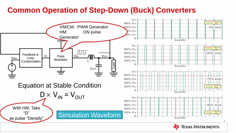
Common Operation of Step-Down (Buck) Converters
COUT
L
PulseModulator
Feedback & Loop-
Compensation
VIN
VOUTVSWVREF
VC
Load
+-
D VIN = VOUT Equation at Stable Condition
VM/CM: PWM Generator
HM: ON pulse
Generator
With HM, Take
“D”
as pulse “Density” Simulation Waveform
4
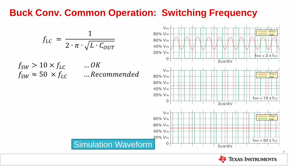
Buck Conv. Common Operation: Switching Frequency
𝑓𝐿𝐶 = 1
2 ∙ 𝜋 ∙ 𝐿 ∙ 𝐶𝑂𝑈𝑇
𝑓𝑆𝑊 > 10 × 𝑓𝐿𝐶 … 𝑂𝐾𝑓𝑆𝑊 ≈ 50 × 𝑓𝐿𝐶 … 𝑅𝑒𝑐𝑜𝑚𝑚𝑒𝑛𝑑𝑒𝑑
Simulation Waveform 5
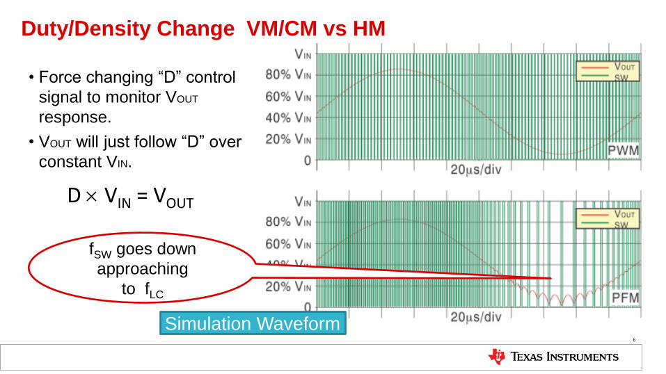
Duty/Density Change VM/CM vs HM
• Force changing “D” control
signal to monitor VOUT
response.
• VOUT will just follow “D” over
constant VIN.
D VIN = VOUT
fSW goes down
approaching
to fLC
Simulation Waveform 6
BUCK CONVERTER COMPENSATION
7
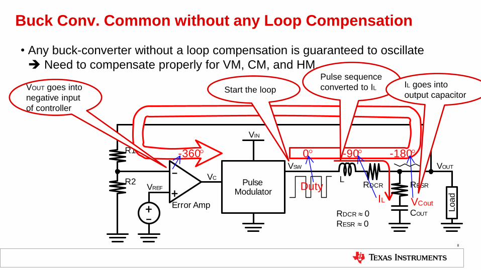
Buck Conv. Common without any Loop Compensation
• Any buck-converter without a loop compensation is guaranteed to oscillate
Need to compensate properly for VM, CM, and HM.
COUT
LPulseModulator
VIN
VOUTVSW
+-
VREF
VC
Load
-180°
DutyIL VCout
RDCR RESR
-90°0°
RDCR » 0
RESR » 0
R1
R2-
+
-360°
Error Amp
Start the loop
Pulse sequence
converted to IL IL goes into
output capacitor VOUT goes into
negative input
of controller
8
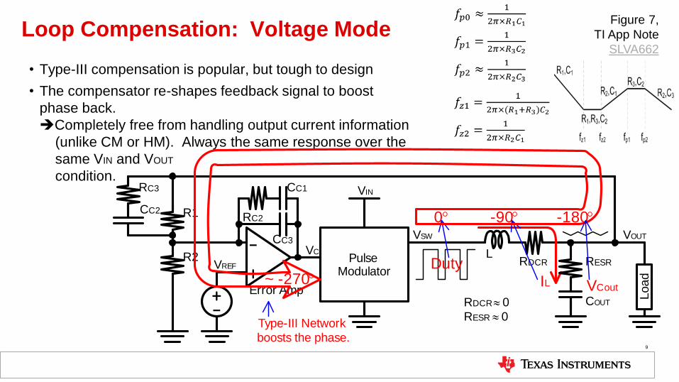
Loop Compensation: Voltage Mode
• Type-III compensation is popular, but tough to design
• The compensator re-shapes feedback signal to boost
phase back.
Completely free from handling output current information
(unlike CM or HM). Always the same response over the
same VIN and VOUT
condition.
COUT
LPulseModulator
VIN
VOUTVSW
+-
VREF
VC
Load
DutyIL VCout
RDCR RESR
-90°0°
RDCR » 0
RESR » 0
R1
R2-
+ ~ -270°Error Amp
-180°
RC3
CC2RC2
CC3
CC1
Type-III Network
boosts the phase.
Figure 7,
TI App Note
SLVA662
9
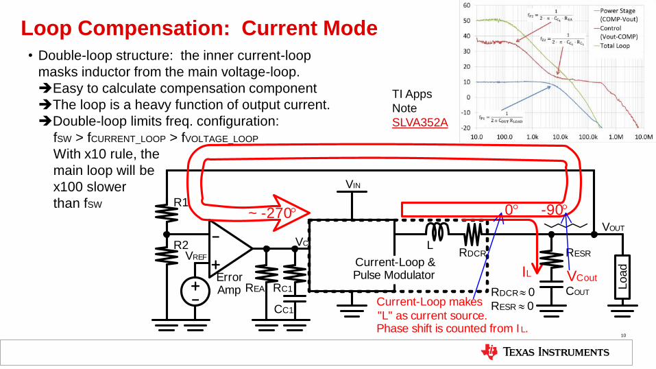
COUT
L
VIN
VOUT
+-
VREF
VC
LoadIL VCout
RDCR RESR
-90°0°
RDCR » 0
RESR » 0
R1
R2-
+
~ -270°
ErrorAmp RC1
CC1Current-Loop makes
"L" as current source.Phase shift is counted from IL.
Current-Loop &Pulse Modulator
REA
Loop Compensation: Current Mode
• Double-loop structure: the inner current-loop
masks inductor from the main voltage-loop.
Easy to calculate compensation component
The loop is a heavy function of output current.
Double-loop limits freq. configuration:
fSW > fCURRENT_LOOP > fVOLTAGE_LOOP
With x10 rule, the
main loop will be
x100 slower
than fSW
TI Apps
Note
SLVA352A
10
COUT
LConstantON
Generator
VIN
VOUTVSW
+-
VREF
VC
Load
DensityIL
RC,CC& CB is dominant feedback in high frequency
RDCR RESR
-90°0°
RDCR » 0
RESR » 0
R1
R2-
+
~ -270°
ErrorComparator
RC CC
Cb
COUT
LConstantON
Generator
VIN
VOUTVSW
+-
VREF
VC
Load
DensityIL
RC,CC& CB is dominant feedback in high frequency
RDCR RESR
-90°0°
RDCR » 0
RESR » 0
R1
R2
-
+
~ -270°
ErrorComparator
RC CC
Cb
-
+ ErrorAmplifier
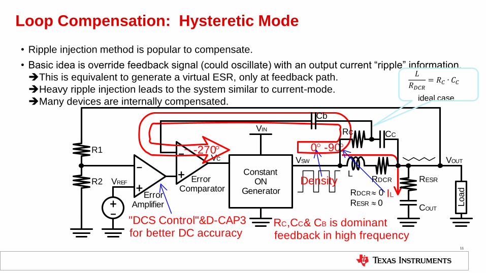
"DCS Control"&D-CAP3for better DC accuracy
Loop Compensation: Hysteretic Mode
• Ripple injection method is popular to compensate.
• Basic idea is override feedback signal (could oscillate) with an output current “ripple” information.
This is equivalent to generate a virtual ESR, only at feedback path.
Heavy ripple injection leads to the system similar to current-mode.
Many devices are internally compensated.
𝐿
𝑅𝐷𝐶𝑅= 𝑅𝐶 ∙ 𝐶𝐶
ideal case
11

Almighty Loop Compensation (Debugging Only)
• Disregarding all other factors, old-days electrolytic capacitors or Tantalum capacitors will bring ultimate stability
due to their high ESR.
• Frequency region above RESR and COUT resonant frequency, the output capacitor turns into resistor, so no 90°
shift.
High ESR system
generates huge
amount of ripple
that is not acceptable
in most of applications.
…not practical…
This method is
very good for a
debugging of
unknown oscillation. COUT
LPulseModulator
VIN
VOUTVSW
+-
VREF
VC
Load
DutyIL VCout
RDCR RESR
-90°0°
RDCR » 0
RESR » 0.1 to 0.2W
R1
R2-
+
-270°
Error Amp
COUT is AC-shorted
in high frequency12

APPLE-TO-APPLE COMPARISON
13
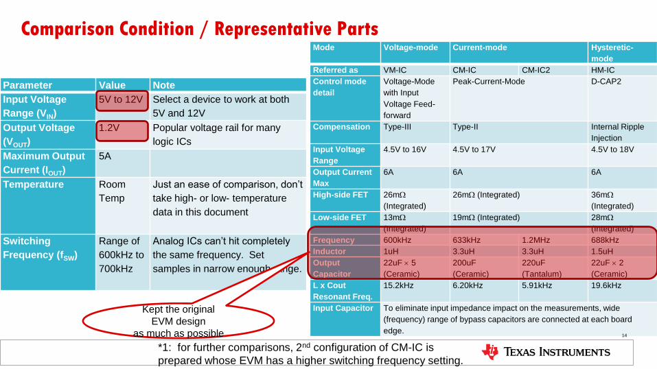
Comparison Condition / Representative Parts
Parameter Value Note
Input Voltage
Range (VIN)
5V to 12V Select a device to work at both
5V and 12V
Output Voltage
(VOUT)
1.2V Popular voltage rail for many
logic ICs
Maximum Output
Current (IOUT)
5A
Temperature Room
Temp
Just an ease of comparison, don’t
take high- or low- temperature
data in this document
Switching
Frequency (fSW)
Range of
600kHz to
700kHz
Analog ICs can’t hit completely
the same frequency. Set
samples in narrow enough range.
Mode Voltage-mode Current-mode Hysteretic-
mode
Referred as VM-IC CM-IC CM-IC2 HM-IC
Control mode
detail
Voltage-Mode
with Input
Voltage Feed-
forward
Peak-Current-Mode D-CAP2
Compensation Type-III Type-II Internal Ripple
Injection
Input Voltage
Range
4.5V to 16V 4.5V to 17V 4.5V to 18V
Output Current
Max
6A 6A 6A
High-side FET 26mW
(Integrated)
26mW (Integrated) 36mW
(Integrated)
Low-side FET 13mW
(Integrated)
19mW (Integrated) 28mW
(Integrated)
Frequency 600kHz 633kHz 1.2MHz 688kHz
Inductor 1uH 3.3uH 3.3uH 1.5uH
Output
Capacitor
22uF 5
(Ceramic)
200uF
(Ceramic)
220uF
(Tantalum)
22uF 2
(Ceramic)
L x Cout
Resonant Freq.
15.2kHz 6.20kHz 5.91kHz 19.6kHz
Input Capacitor To eliminate input impedance impact on the measurements, wide
(frequency) range of bypass capacitors are connected at each board
edge. 14
Kept the original
EVM design
as much as possible
*1: for further comparisons, 2nd configuration of CM-IC is
prepared whose EVM has a higher switching frequency setting.
LARGE SIGNAL LOAD TRANSIENT RESPONSE PART 1: BASIC COMPARISON
Apple-to-apple comparison
15
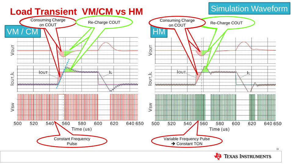
Load Transient VM/CM vs HM
Constant Frequency
Pulse
Variable Frequency Pulse
Constant TON
VM / CM HM
Consuming Charge
on COUT Re-Charge COUT
Simulation Waveform
16
Re-Charge COUT Consuming Charge
on COUT
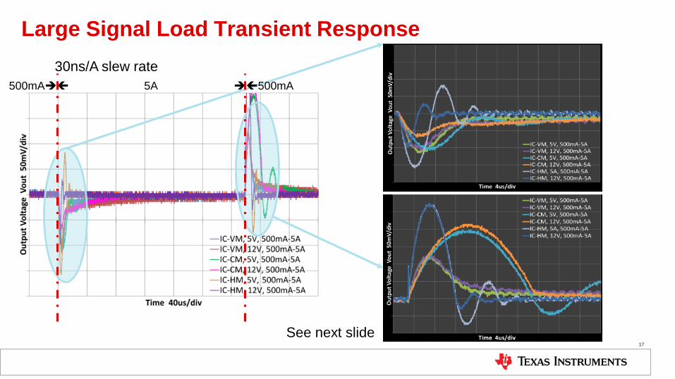
Large Signal Load Transient Response
30ns/A slew rate
See next slide
500mA 5A 500mA
17
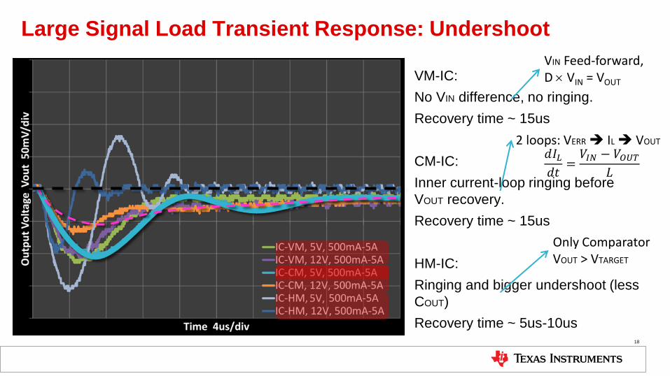
Large Signal Load Transient Response: Undershoot
VM-IC:
No VIN difference, no ringing.
Recovery time ~ 15us
CM-IC:
Inner current-loop ringing before
VOUT recovery.
Recovery time ~ 15us
HM-IC:
Ringing and bigger undershoot (less
COUT)
Recovery time ~ 5us-10us
VIN Feed-forward, D VIN = VOUT
𝑑𝐼𝐿
𝑑𝑡=
𝑉𝐼𝑁 − 𝑉𝑂𝑈𝑇
𝐿
2 loops: VERR IL VOUT
Only Comparator VOUT > VTARGET
18
LARGE SIGNAL LOAD TRANSIENT RESPONSE PART 2: COMPARISON OF VARIOUS PARAMETERS
Apple-to-apple comparison
19
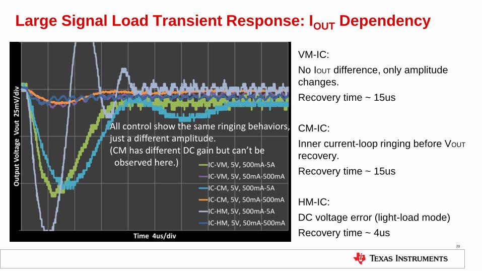
Large Signal Load Transient Response: IOUT Dependency
VM-IC:
No IOUT difference, only amplitude
changes.
Recovery time ~ 15us
CM-IC:
Inner current-loop ringing before VOUT
recovery.
Recovery time ~ 15us
HM-IC:
DC voltage error (light-load mode)
Recovery time ~ 4us
All control show the same ringing behaviors, just a different amplitude. (CM has different DC gain but can’t be observed here.)
20
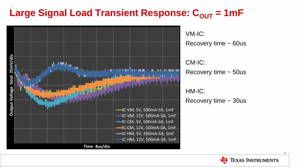
Large Signal Load Transient Response: COUT = 1mF
VM-IC:
Recovery time ~ 60us
CM-IC:
Recovery time ~ 50us
HM-IC:
Recovery time ~ 30us
21
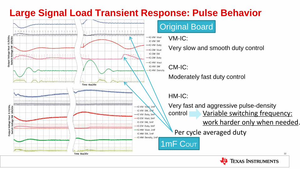
Large Signal Load Transient Response: Pulse Behavior
VM-IC:
Very slow and smooth duty control
CM-IC:
Moderately fast duty control
HM-IC:
Very fast and aggressive pulse-density
control
Original Board
1mF COUT
Per cycle averaged duty
Variable switching frequency: work harder only when needed.
22
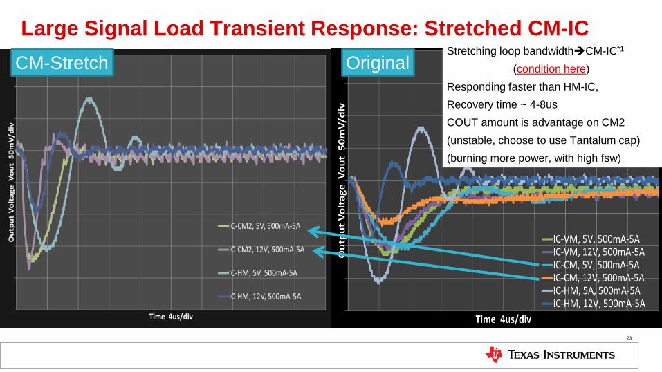
Large Signal Load Transient Response: Stretched CM-IC Stretching loop bandwidthCM-IC*1
(condition here)
Responding faster than HM-IC,
Recovery time ~ 4-8us
COUT amount is advantage on CM2
(unstable, choose to use Tantalum cap)
(burning more power, with high fsw)
CM-Stretch Original
23
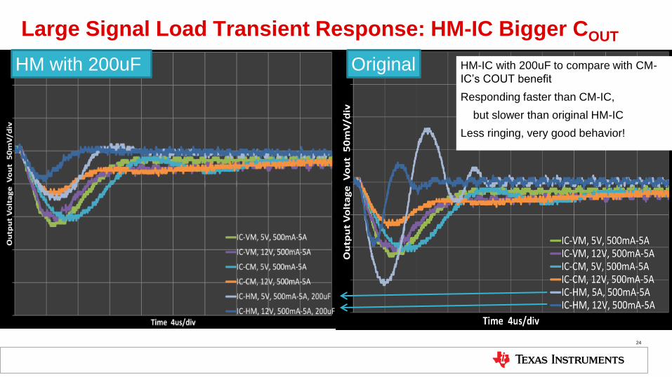
Large Signal Load Transient Response: HM-IC Bigger COUT
HM with 200uF Original HM-IC with 200uF to compare with CM-
IC’s COUT benefit
Responding faster than CM-IC,
but slower than original HM-IC
Less ringing, very good behavior!
24
LINE TRANSIENT RESPONSE Apple-to-apple comparison
25

Line Transient Response
VM-IC:
Smooth waveforms
Recovery time ~ 40us
CM-IC:
Edge of stability (0.1uF input cap)
Recovery time ~ 80us
HM-IC:
Perfect response
Recovery time (can’t observe
glitches)
26

LOOP STABILITY / SMALL SIGNAL STUDY VOLTAGE-MODE
Apple-to-apple comparison
27
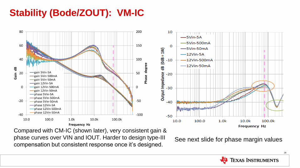
Stability (Bode/ZOUT): VM-IC
See next slide for phase margin values
Compared with CM-IC (shown later), very consistent gain &
phase curves over VIN and IOUT. Harder to design type-III
compensation but consistent response once it’s designed.
28
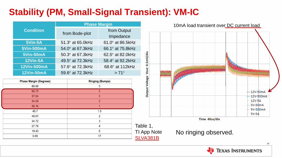
Stability (PM, Small-Signal Transient): VM-IC
Condition
Phase Margin
from Bode-plot from Output
Impedance
5Vin-5A 51.3° at 65.0kHz 61.0° at 86.5kHz
5Vin-500mA 54.0° at 67.3kHz 66.1° at 75.8kHz
5Vin-50mA 50.3° at 67.3kHz 62.5° at 82.0kHz
12Vin-5A 49.5° at 72.3kHz 58.4° at 92.2kHz
12Vin-500mA 57.6° at 72.3kHz 68.6° at 112kHz
12Vin-50mA 59.6° at 72.3kHz > 71°
Table 1,
TI App Note
SLVA381B
10mA load transient over DC current load
No ringing observed.
29
LOOP STABILITY / SMALL SIGNAL STUDY CURRENT-MODE
Apple-to-apple comparison
30

Stability (Bode/ZOUT): CM-IC
Loop response changes a lot by VIN, IOUT.
It’s challenging to support wide changing operation range. See next slide for phase margin values
31
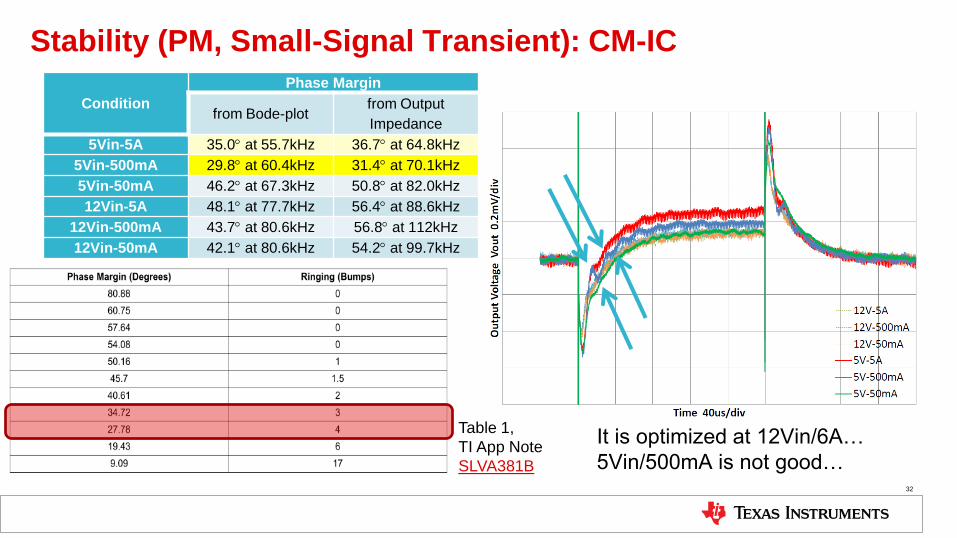
Stability (PM, Small-Signal Transient): CM-IC
Condition
Phase Margin
from Bode-plot from Output
Impedance
5Vin-5A 35.0° at 55.7kHz 36.7° at 64.8kHz
5Vin-500mA 29.8° at 60.4kHz 31.4° at 70.1kHz
5Vin-50mA 46.2° at 67.3kHz 50.8° at 82.0kHz
12Vin-5A 48.1° at 77.7kHz 56.4° at 88.6kHz
12Vin-500mA 43.7° at 80.6kHz 56.8° at 112kHz
12Vin-50mA 42.1° at 80.6kHz 54.2° at 99.7kHz
Table 1,
TI App Note
SLVA381B
It is optimized at 12Vin/6A…
5Vin/500mA is not good… 32
LOOP STABILITY / SMALL SIGNAL STUDY HYSTERETIC-MODE
Apple-to-apple comparison
33
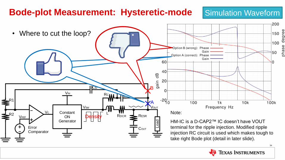
Bode-plot Measurement: Hysteretic-mode
COUT
LConstantON
Generator
VIN
VOUTVSW
+-
VREF
VC
Load
Density RDCR RESR
R1
R2-
+
ErrorComparator
RC CC
Cb
A
B
• Where to cut the loop?
Note:
HM-IC is a D-CAP2™ IC doesn’t have VOUT
terminal for the ripple injection. Modified ripple
injection RC circuit is used which makes tough to
take right Bode plot (detail in later slide).
Simulation Waveform
34
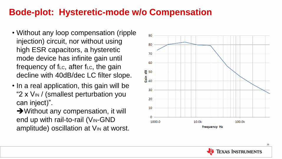
• Without any loop compensation (ripple
injection) circuit, nor without using
high ESR capacitors, a hysteretic
mode device has infinite gain until
frequency of fLC, after fLC, the gain
decline with 40dB/dec LC filter slope.
• In a real application, this gain will be
“2 x VIN / (smallest perturbation you
can inject)”.
Without any compensation, it will
end up with rail-to-rail (VIN-GND
amplitude) oscillation at VIN at worst.
Bode-plot: Hysteretic-mode w/o Compensation
35
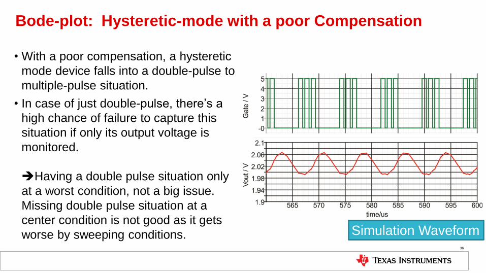
• With a poor compensation, a hysteretic
mode device falls into a double-pulse to
multiple-pulse situation.
• In case of just double-pulse, there’s a
high chance of failure to capture this
situation if only its output voltage is
monitored.
Having a double pulse situation only
at a worst condition, not a big issue.
Missing double pulse situation at a
center condition is not good as it gets
worse by sweeping conditions.
Bode-plot: Hysteretic-mode with a poor Compensation
Simulation Waveform 36
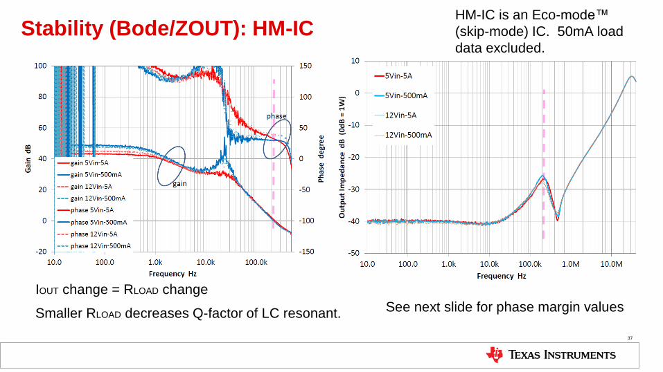
Stability (Bode/ZOUT): HM-IC
IOUT change = RLOAD change
Smaller RLOAD decreases Q-factor of LC resonant. See next slide for phase margin values
HM-IC is an Eco-mode™
(skip-mode) IC. 50mA load
data excluded.
37
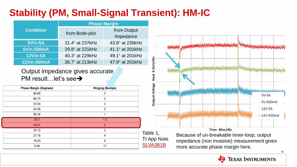
Stability (PM, Small-Signal Transient): HM-IC
Condition
Phase Margin
from Bode-plot from Output
Impedance
5Vin-5A 31.4° at 237kHz 43.6° at 236kHz
5Vin-500mA 29.8° at 221kHz 41.1° at 201kHz
12Vin-5A 40.3° at 229kHz 49.1° at 201kHz
12Vin-500mA 36.7° at 213kHz 47.9° at 201kHz
Table 1,
TI App Note
SLVA381B
Because of un-breakable inner-loop, output
impedance (non invasive) measurement gives
more accurate phase margin here.
Output impedance gives accurate
PM result…let’s see
38

Questions?
39