comparator
TRANSCRIPT

• GROUP:2• Op-amp as a comparator• ENROLL NO:• 131100109006 DOCTOR MOHAMAD SHAFI MOHAMAD HARUN• 131100109010 GUPTA SAGAR• 131100109033 PATEL HIREN• 131100109015 MANSUR SHAHBAZ M• 131100109013 KHOLIA BHAVESH
• GUIDED BY ROHIT B DAMOR
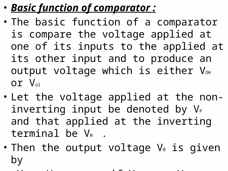
• Basic function of comparator :• The basic function of a comparator is compare the
voltage applied at one of its inputs to the applied at its other input and to produce an output voltage which is either VOH or Vol
• Let the voltage applied at the non-inverting input be denoted by VP and that applied at the inverting terminal be VN .
• Then the output voltage V0 is given by • V0 = VOH ….if V p > V n• V0 = Vol ….if V p < V n

• .

• Types of comparator :• 1 : non –inverting 2: inverting comparator Non –invarting compatetor:• The schematic diagram of a non inverting
competitor is as showing in fig.• A positive dc reference voltage is applied to the
inverting terminal (-) and an ac sinusoidal signal is applied to the non inverting(+) terminal.
• As the signal is connected to the non inverting (+) terminal , this comparator as non inverting comparator


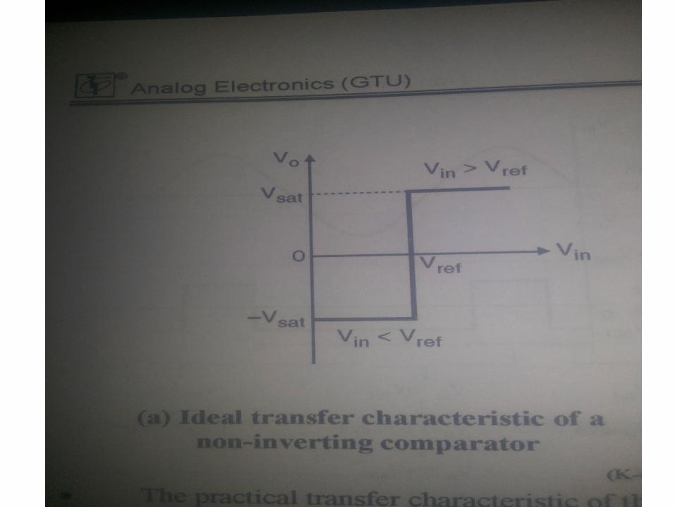
• Transfer characteristic of non inverting comparator :
• The ideal transfer characteristic of a non inverting comparator is shown in figure 1.
• It shows that the output is equal to –V sat for V in < V ref and switches to +V sat as soon as Vin is slightly grater than V ref .
• The differential voltage needed to switch the state of output is ideally zero .
• The practical transfer characteristic of the commercial OP-AMP is shown in figure 2.
• The change in output state takes place when the differential voltage is about 2mV.

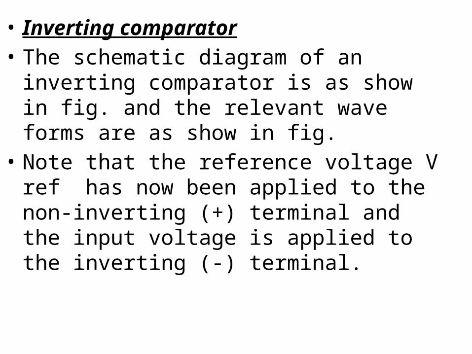
• Inverting comparator• The schematic diagram of an inverting
comparator is as show in fig. and the relevant wave forms are as show in fig.
• Note that the reference voltage V ref has now been applied to the non-inverting (+) terminal and the input voltage is applied to the inverting (-) terminal.


• Transfer characteristic of an inverting comparator :• Figure 1 shows the ideal transfer characteristic of an
inverting comparator .• It shows that the output voltage is equal to +V sat
for Vin less than V ref .it switches instantaneously from +V sat to –V sat when Vin becomes just slightly grater than V ref
• The differential voltage needed for switching the output state is very small , ideally it is zero volt.
• The commercial OP- AMP have the transfer characteristic as shown in figure 2.
• The change in output state takes place when the differential voltage is about 2mV.


• ZERO CROSSING DETECTOR :• Zero crossing detector is shown in figure .as we can
see, zero crossing detector is nothing but the basic comparator circuit with a zero reference voltage applied to the non-inverting terminal.
• Refer to the waveforms shown in figure .when the input sine wave crosses zero and becomes positive at instant t=0 ,the differential input voltage Vd becomes negative and the output voltage will swing to –V sat .
• when the sine wave again crosses zero and becomes negative at instant t=T/2.


• The differential input voltage becomes positive and the output voltage will swing to +V sat as now the (+) terminal is more positive than the (-) terminal .
• The zero crossing detector thus switches its output from one state to other every time when the input voltage crosses the zero .
• The zero crossing detector is also known as a sinewave to square wave converter .

• Thank you….