compactblock ldx rtd/resistance input module user...
TRANSCRIPT

CompactBlock LDX RTD/Resistance Input Module1790D-4R0, 1790D-T4R0, 1790P-T4R0
User Manual

Important User Information Because of the variety of uses for the products described in this publication, those responsible for the application and use of these products must satisfy themselves that all necessary steps have been taken to assure that each application and use meets all performance and safety requirements, including any applicable laws, regulations, codes and standards. In no event will Allen-Bradley be responsible or liable for indirect or consequential damage resulting from the use or application of these products.
Any illustrations, charts, sample programs, and layout examples shown in this publication are intended solely for purposes of example. Since there are many variables and requirements associated with any particular installation, Allen-Bradley does not assume responsibility or liability (to include intellectual property liability) for actual use based upon the examples shown in this publication.
Allen-Bradley publication SGI-1.1, Safety Guidelines for the Application, Installation and Maintenance of Solid-State Control (available from your local Allen-Bradley office), describes some important differences between solid-state equipment and electromechanical devices that should be taken into consideration when applying products such as those described in this publication.
Reproduction of the contents of this copyrighted publication, in whole or part, without written permission of Rockwell Automation, is prohibited.
Throughout this publication, notes may be used to make you aware of safety considerations. The following annotations and their accompanying statements help you to identify a potential hazard, avoid a potential hazard, and recognize the consequences of a potential hazard:
RSNetWorx, RSNetWorx for DeviceNet, RSLogix 500, and RSLogix 5000 are trademarks of Rockwell Automation.
Belden is a trademark of Belden, Inc.
WARNING
!Identifies information about practices or circumstances that can cause an explosion in a hazardous environment, which may lead to personal injury or death, property damage, or economic loss.
ATTENTION
!Identifies information about practices or circumstances that can lead to personal injury or death, property damage, or economic loss.

Rockwell Automation Support
Before you contact Rockwell Automation for technical assistance, we suggest you please review the troubleshooting information contained in this publication first.
If the problem persists, call your local Rockwell Automation representative or contact Rockwell Automation in one of the following ways:
Your Questions or Comments on this Manual
If you find a problem with this manual, please notify us by using the enclosed How Are We Doing form.
IMPORTANT Identifies information that is critical for successful application and understanding of the product.
Phone United States/Canada
1.440.646.5800
Outside United States/Canada
You can access the phone number for your country via the Internet:
1. Go to http://www.ab.com2. Click on Product Support
(http://support.automation.rockwell.com)3. Under Support Centers, click on Contact
Information
Internet 1. Go to http://www.ab.com2. Click on Product Support
(http://support.automation.rockwell.com)

i Publication 1790-UM002A-EN-P - May 2002
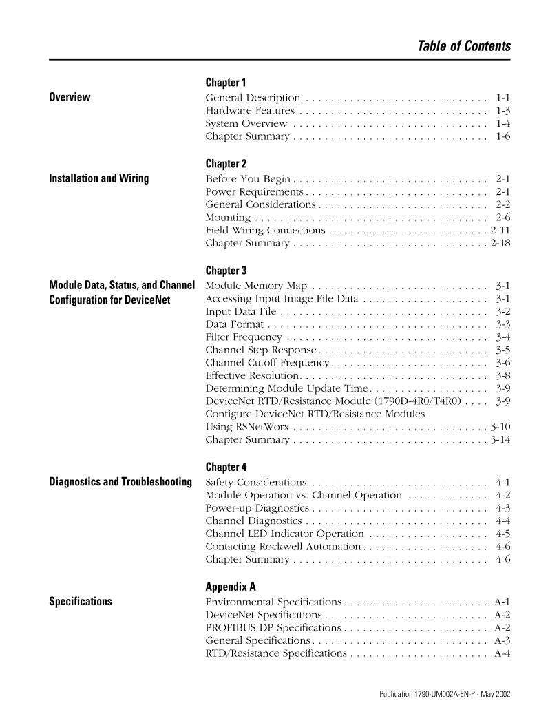
Table of Contents
Chapter 1Overview General Description . . . . . . . . . . . . . . . . . . . . . . . . . . . . . 1-1
Hardware Features . . . . . . . . . . . . . . . . . . . . . . . . . . . . . . 1-3System Overview . . . . . . . . . . . . . . . . . . . . . . . . . . . . . . . 1-4Chapter Summary . . . . . . . . . . . . . . . . . . . . . . . . . . . . . . . 1-6
Chapter 2Installation and Wiring Before You Begin . . . . . . . . . . . . . . . . . . . . . . . . . . . . . . . 2-1
Power Requirements . . . . . . . . . . . . . . . . . . . . . . . . . . . . . 2-1General Considerations . . . . . . . . . . . . . . . . . . . . . . . . . . . 2-2Mounting . . . . . . . . . . . . . . . . . . . . . . . . . . . . . . . . . . . . . 2-6Field Wiring Connections . . . . . . . . . . . . . . . . . . . . . . . . . 2-11Chapter Summary . . . . . . . . . . . . . . . . . . . . . . . . . . . . . . . 2-18
Chapter 3Module Data, Status, and Channel Configuration for DeviceNet
Module Memory Map . . . . . . . . . . . . . . . . . . . . . . . . . . . . 3-1Accessing Input Image File Data . . . . . . . . . . . . . . . . . . . . 3-1Input Data File . . . . . . . . . . . . . . . . . . . . . . . . . . . . . . . . . 3-2Data Format . . . . . . . . . . . . . . . . . . . . . . . . . . . . . . . . . . . 3-3Filter Frequency . . . . . . . . . . . . . . . . . . . . . . . . . . . . . . . . 3-4Channel Step Response . . . . . . . . . . . . . . . . . . . . . . . . . . . 3-5Channel Cutoff Frequency . . . . . . . . . . . . . . . . . . . . . . . . . 3-6Effective Resolution. . . . . . . . . . . . . . . . . . . . . . . . . . . . . . 3-8Determining Module Update Time. . . . . . . . . . . . . . . . . . . 3-9DeviceNet RTD/Resistance Module (1790D-4R0/T4R0) . . . . 3-9Configure DeviceNet RTD/Resistance Modules Using RSNetWorx . . . . . . . . . . . . . . . . . . . . . . . . . . . . . . . 3-10Chapter Summary . . . . . . . . . . . . . . . . . . . . . . . . . . . . . . . 3-14
Chapter 4Diagnostics and Troubleshooting Safety Considerations . . . . . . . . . . . . . . . . . . . . . . . . . . . . 4-1
Module Operation vs. Channel Operation . . . . . . . . . . . . . 4-2Power-up Diagnostics . . . . . . . . . . . . . . . . . . . . . . . . . . . . 4-3Channel Diagnostics . . . . . . . . . . . . . . . . . . . . . . . . . . . . . 4-4Channel LED Indicator Operation . . . . . . . . . . . . . . . . . . . 4-5Contacting Rockwell Automation . . . . . . . . . . . . . . . . . . . . 4-6Chapter Summary . . . . . . . . . . . . . . . . . . . . . . . . . . . . . . . 4-6
Appendix ASpecifications Environmental Specifications . . . . . . . . . . . . . . . . . . . . . . . A-1
DeviceNet Specifications . . . . . . . . . . . . . . . . . . . . . . . . . . A-2PROFIBUS DP Specifications . . . . . . . . . . . . . . . . . . . . . . . A-2General Specifications . . . . . . . . . . . . . . . . . . . . . . . . . . . . A-3RTD/Resistance Specifications . . . . . . . . . . . . . . . . . . . . . . A-4

Publication 1790-UM002A-EN-P - May 2002
Table of Contents ii
Appendix BTwo’s Complement Binary Numbers
Positive Decimal Values . . . . . . . . . . . . . . . . . . . . . . . . . . B-1Negative Decimal Values . . . . . . . . . . . . . . . . . . . . . . . . . . B-2
Appendix CModule Configuration for PROFIBUS
Configure PROFIBUS RTD/Resistance Modules (1790P-T4R0) . . . . . . . . . . . . . . . . . . . . . . . . . . . . . . . . . . C-1Configure RTD/Resistance Modules Using the SST PROFIBUS Configuration Tool . . . . . . . . . . . . . . . . . . . . . . . . . . . . . . C-1Save the Configuration . . . . . . . . . . . . . . . . . . . . . . . . . . . C-6Download the Configuration . . . . . . . . . . . . . . . . . . . . . . . C-7Summary . . . . . . . . . . . . . . . . . . . . . . . . . . . . . . . . . . . . . C-9

1 Publication 1790-UM002A-EN-P
Chapter 1
Overview
This chapter describes the four-channel 1790D-4R0/T4R0 RTD/resistance Input module and explains how the controller reads resistance temperature detector (RTD) or direct resistance-initiated analog input data from the module. Included is:
• a general description of hardware features
• an overview of module and system operation
• compatibility
General Description The 1790D-4R0/T4R0 (1790P-T4R0) module supports RTD and direct resistance signal measurement applications that require up to four channels. The module digitally converts analog data and then stores the converted data in its image table.
The module supports connections from any combination of up to four input devices. Each channel is individually configurable via software for 2- or 3-wire RTD or direct resistance input devices. Channels are compatible with 4-wire sensors, but the fourth sense wire is not used. When configured for RTD inputs, the module can convert the RTD readings into linearized digital temperature readings in °C or °F. When configured for resistance analog inputs, the module can convert voltages into linearized resistance values in ohms. The module assumes that the direct resistance input signal is linear prior to input to the module.
Each channel provides open-circuit (all wires) and over- and under-range detection and indication.
IMPORTANT The module accepts input from RTDs with up to 3 wires. If your application requires a 4-wire RTD, one of the two lead compensation wires is not used, and the RTD is treated like a 3-wire sensor. The third wire provides lead wire compensation. See Chapter 2, Installation and Wiring, for more information.

Publication 1790-UM002A-EN-P
1-2 Overview
The module supports the following filter frequencies:
• 10 Hz
• 25 Hz
• 50 Hz
• 60 Hz
• 100 Hz
• 250 Hz
• 500 Hz
The module uses five input words for data and status bits. Module configuration is stored in the module memory. Configuration for 1790D-(T)4R0 is done via RSNetWorx for DeviceNet™ programming software. See Chapter 3, Module Data, Status, and Channel Configuration, for details on module configuration. Configuration for 1790P-T4R0 is done via PROFIBUS configuration software. See Appendix C for details.
RTD Compatibility
An RTD consists of a temperature-sensing element connected by two, three, or four wires that provide input to the module. The following table lists the RTD types that you can use with the module, including their temperature range, effective resolution, and accuracy.
Table 1.1 RTD Specifications
RTD Type Temperature Range
Scaling (Counts)
Resolution* Accuracy** (0 to 55°C)
100ohm Pt/α=0.00385 -200 to +850°C -2000 to +8500 0.1°C ±2.1°C
200ohm Pt/α=0.00385 -200 to +850°C -2000 to +8500 0.1°C ±2.1°C
500ohm Pt/α=0.00385 -200 to +650°C -2000 to +6500 0.1°C ±1.7°C
100ohm Pt/α=0.003916 -200 to +640°C -2000 to +6400 0.1°C ±1.68°C
200ohm Pt/α=0.003916 -200 to +640°C -2000 to +6400 0.1°C ±1.68°C
500ohm Pt/α=0.003916 -200 to +640°C -2000 to +6400 0.1°C ±1.68°C
100ohm Nickel -60 to 250°C -600 to 2500°C 0.1 °C ±0.62°C
120ohm Nickel -80 to 260°C -800 to 2600 0.1°C ±0.68°C
200ohm Nickel -60C to 250°C -600 to 2500 0.1°C ±1.62°C
500ohm Nickel -60 to 250°C -600 to 2500 0.1°C ±0.62°C
*Filter set for 10 Hz3
**Module only

Publication 1790-UM002A-EN-P
Overview 1-3
Resister Device Compatibility
The following table lists the specifications for the resistance devices that you can use with the module.
Hardware Features The RTD/resistance module contains either a fixed terminal block (or a removable D-sub connector) providing connections for four 3-wire inputs for any combination of RTD and resistance input devices. Channels are wired as differential inputs. The illustration below shows the hardware features of the module.
Table 1.2 Resistance Device Specifications
Resistance Type Range Scaling (Counts)
Resolution* Accuracy (0 to 55°C)**
Resistance 100mΩ 1 to 650Ω 10 to 6250 100mΩ +1.25Ω
Resistance 10mΩ 1 to 327Ω 100 to 32700 10Ω +0.65Ω
*Filter set for 10 Hz**Module only
Node Address Switches
Module and Network Status Indicators
43223
1790D-4R0/T4R0 DeviceNet Module
RTD/resistance Channel Indicators
RTD/resistance Connections (D-sub Connector shown)
CompactBlock LDX 1790D-8BV8V
8 INPUTS/8OUTPUTS-DC POWER
07 0
7DeviceNet Network Connection
DIN Rail Slot
Panel Mount Hole

Publication 1790-UM002A-EN-P
1-4 Overview
General Diagnostic Features
Module, network, and channel LEDs help you identify the source of problems that may occur during power-up or during normal channel operation. The LEDs indicate both status and power. See Chapter 4, Diagnostics and Troubleshooting, for details on power-up and channel diagnostics.
System Overview The modules communicate to the controller or network scanner via the DeviceNet™ or PROFIBUS network. The modules also receive 24V dc power through DeviceNet. An external 24V dc auxiliary source is required to power the RTD/resistance channels.
System Operation
At power-up, the module performs a check of its internal circuits, memory, and basic functions. If no faults are found during power-up diagnostics, the module status LED is turned on (green).
Node Address Switches
Module and Network Status Indicators Panel Mount
Hole
RTD/resistance Channel Indicators
RTD/resistance Connections (Terminal block)
PROFIBUS Network Connector
DIN Rail Slot
Module Power Connector (underneath module)
PROFIBUS Connector
31341-M
1790P-T4R0 PROFIBUS DP Module

Publication 1790-UM002A-EN-P
Overview 1-5
Once a channel is properly configured and enabled, the module continuously converts the RTD or resistance input to a value within the range selected for that channel.
Each time the module reads an input channel, it tests the data for a fault (over- or under-range or open-circuit condition). If it detects a fault, the module sets a unique bit in the channel status word. See Input Data File on page 3-2. The module sends two’s compliment binary converted RTD/resistance data out over the network. See Appendix B for a description of two’s compliment binary numbers.
Module Operation - DeviceNet Example
As shown in the block diagram below, each input channel of the module consists of an RTD/resistance connection that accepts excitation current; a sense connection that detects lead wire resistance; and a return connection. The signals are multiplexed to an A/D converter that reads the RTD or resistance value and the lead wire resistance.
From the readings taken by the converter, the module sends RTD or resistance data through the microcontroller to the DeviceNet network.
The PROFIBUS block diagram is similar.
Input
EXC0
SENSE0
RTN0
CH0
Multiplexer
VA2
A/D
VREFVref
Channel Select
Channels 1 through 3 same as channel 0 above.
43224
A
B
COM
VA1 VA1EXCCurrent
VccOpticalIsolation
AIN-
AIN+2
AIN+1
VA3
A-GND
Micro- Controller
Transmit
Receive
GND
Network
PowerSupply
AnalogPowerSupply DeviceNet
24Vdc Power
Vcc
GND
VA1VA2VA3
A-GND
VDC
GND
1
2
3
Auxiliary24Vdc Power

Publication 1790-UM002A-EN-P
1-6 Overview
Chapter Summary In this chapter, you learned about the 1790D/4R0/T4R0 and 1790P-TR40 RTD/resistance modules. See Chapter 2 to learn how to install and wire the modules.

1 Publication 1790-UM002A-EN-P
Chapter 2
Installation and Wiring
Before You Begin This chapter tells you how to:
• determine the power requirements for the modules
• avoid electrostatic damage
• install the module
• wire the module’s terminal block
Power Requirements 1790D-4R0/T4R0
The module receives system power from the DeviceNet network. An auxiliary field supply provides power for the RTD/resistance channels.
1790P-T4R0
The module requires external supplies for both system power and for the RTD/resistance channels.
Table 2.1 1790D-4R0/T4R0 Power Specifications
Power SpecificationDeviceNet Supply voltage - 24V dc nominal
Voltage range - 11-28.8V dcPower dissipation - 1.2W maximum @ 28.8V dc
Field Supply voltage - 24V dc nominalVoltage range - 21.6-26.4V dc (+10%)Power dissipation - 1.5W maximum @ 26.4V dc
Table 2.2 1790P-T4R0 Power Specifications
Power SpecificationPROFIBUS Supply voltage - 24V dc nominal
Voltage range - 19.2-28.8V dcPower dissipation - 2W maximum @ 28.8V dc
Field Supply voltage - 24V dc nominalVoltage range - 21.6-26.4V dc (+10%)Power dissipation - 1.5W maximum @ 26.4V dc

Publication 1790-UM002A-EN-P
2-2 Installation and Wiring
General Considerations The modules are suitable for use in a commercial or light industrial environment when installed in accordance with these instructions. Specifically, this equipment is intended for use in clean, dry environments
(Pollution degree 2(1)) and to circuits not exceeding Over Voltage
Category II(2) (IEC 60664-1).(3)
Hazardous Location Considerations
This equipment is suitable for use in Class I, Division 2, Groups A, B, C, D or non-hazardous locations only. The following WARNING statement applies to use in hazardous locations.
(1) Pollution Degree 2 is an environment where, normally, only non-conductive pollution occurs except that occasionally a temporary conductivity caused by condensation shall be expected.
(2) Over Voltage Category II is the load level section of the electrical distribution system. At this level transient voltages are controlled and do not exceed the impulse voltage capability of the product’s insulation.
(3) Pollution Degree 2 and Over Voltage Category II are International Electrotechnical Commission (IEC) designations.
WARNING
ÿEXPLOSION HAZARD
• Substitution of components may impair suitability for Class I, Division 2.
• Do not replace components or disconnect equipment unless power has been switched off or the area is known to be non-hazardous.
• Do not connect or disconnect components unless power has been switched off or the area is known to be non-hazardous.
• This product must be installed in an enclosure.• All wiring must comply with N.E.C. article 501-4(b).

Publication 1790-UM002A-EN-P
Installation and Wiring 2-3
ATTENTION
ÿ
Environment and Enclosure
This equipment is intended for use in a Pollution Degree 2 industrial environment, in overvoltage Category II applications (as defined in IEC publication 60664-1), at altitudes up to 2000 meters without derating.
This equipment is considered Group 1, Class A industrial equipment according to IEC/CISPR Publication 11. Without appropriate precautions, there may be potential difficulties ensuring electromagnetic compatibility in other environments due to conducted as well as radiated disturbance.
This equipment is supplied as "open type" equipment. It must be mounted within an enclosure that is suitably designed for those specific environmental conditions that will be present and appropriately designed to prevent personal injury resulting from accessibility to live parts. The interior of the enclosure must be accessible only by the use of a tool. Subsequent sections of this publication may contain additional information regarding specific enclosure type ratings that are required to comply with certain product safety certifications.
See NEMA Standards publication 250 and IEC publication 60529, as applicable, for explanations of the degrees of protection provided by different types of enclosure. Also, see the appropriate sections in this publication, as well as the Allen-Bradley publication 1770-4.1 ("Industrial Automation Wiring and Grounding Guidelines"), for additional installation requirements pertaining to this equipment.

Publication 1790-UM002A-EN-P
2-4 Installation and Wiring
Selecting a Location
Reducing Noise
Most applications require installation in an industrial enclosure to reduce the effects of electrical interference. RTD inputs are highly susceptible to electrical noise. Electrical noise coupled to the RTD inputs will reduce the performance (accuracy) of the module.
Group your modules in the enclosure to minimize adverse effects from radiated electrical noise and heat. Consider the following conditions when selecting a location for the module. Position the module:
• away from sources of electrical noise such as hard-contact switches, relays, and AC motor drives
• away from modules which generate significant radiated heat.
In addition, route shielded, twisted-pair wiring away from any high voltage I/O wiring.
ATTENTION
ÿ
Preventing Electrostatic Discharge
This equipment is sensitive to electrostatic discharge, which can cause internal damage and affect normal operation. Follow these guidelines when you handle this equipment:
• Touch a grounded object to discharge potential static.• Wear an approved grounding wriststrap.• Do not touch connectors or pins on component
boards.• Do not touch circuit components inside the equipment.• If available, use a static-safe workstation.• When not in use, store the equipment in appropriate
static-safe packaging.
WARNING
ÿIf you insert or remove the module while power is on, an electrical arc can occur. This could cause an explosion in hazardous location installations.
Be sure that power is removed or the area is nonhazardous before proceeding.

Publication 1790-UM002A-EN-P
Installation and Wiring 2-5
Protecting the Circuit Board from Contamination
The printed circuit boards of analog modules must be protected from dirt, oil, moisture, and other airborne contaminants. To protect these boards, the system must be installed in an enclosure suitable for the environment. The interior of the enclosure should be kept clean and the enclosure door should be kept closed whenever possible.
Installing CompactBlock LDX I/O
Follow these steps to install the block:
1. Set the node address on the base block.
2. Mount the base block.
3. Wire the terminal blocks.
4. Connect the network cable.
These steps are explained in detail in the following procedures for both the 1790D-4R0/T4R0 DeviceNet and 1790P-T4R0 PROFIBUS DP modules.
Set the Node Address on the DeviceNet 1790D-4R0/T4R0 Base Block
Each base block comes with its internal program set for node address 63. To reset the node address, adjust the switches on the front of the block. The two switches are most significant digit (MSD) and least significant digit (LSD). The switches can be set between 00 and 63.
The rotary switches are read at block power up only. Switch settings between 64 and 99 cause the block to use the last valid node address stored internally.
The node address may also be set through RSNetWorx for DeviceNet or a similar configuration tool. When software configuration is used for the node address, the switches must be set between 64 and 99.
Example: Node Address is set at 26
43230

Publication 1790-UM002A-EN-P
2-6 Installation and Wiring
Set the Station Address on the 1790P-T4R0 PROFIBUS DP Base Block
To set the station address, adjust the switches on the front of the base block. The two switches are most significant digit (MSD) and least significant digit (LSD). The switches can be set between 00 and 99.
The rotary switches are read at base block power up only.
Mounting Mount the Base Block
You can mount the base block to a panel or DIN rail. We recommend that you ground the panel or DIN rail before mounting the block.
Panel Mounting1. Place the block against the panel where you want to mount it.
2. Gently pull and position the expansion cover to the left.
3. Place a center punch, nail or similar device through the mounting holes in the block and make two marks on the panel (lower left and upper right corners of the module).
4. Remove the block and drill two holes in the panel to accommodate each of the mounting screws.
Example: Node Address is set at 26
43230
IMPORTANT The RTD and thermocouple base modules do not support any expansion blocks.
WARNING
ÿWhen used in a Class I, Division 2, hazardous location, this equipment must be mounted in a suitable enclosure with proper wiring method that complies with the governing electrical codes.

Publication 1790-UM002A-EN-P
Installation and Wiring 2-7
5. Replace the block on the panel and place a screw through each of the two mounting holes. Tighten the screws until the block is firmly in place.
DIN Rail Mounting1. Hook the top slot of the block over the DIN Rail.
2. Pull down on the locking lever while pressing the block against the rail.
3. Push up on the locking lever to secure the block to the rail when the block is flush against the rail.
CompactBlock LDX 1790-16BVOX
EXPANSION UNIT
16 INPUTS-DCPOWER
0 7 0
7
41 mm1.6 in
95 mm3.74 in
ExpansionCover
43242
Locking Lever
ÿ
43243

Publication 1790-UM002A-EN-P
2-8 Installation and Wiring
Connect the DeviceNet Cable to the 1790D-4R0/T4R0 Base Block
Follow these procedures when connecting the DeviceNet cable to the base block.
The required DeviceNet connector is not supplied with the block - you must purchase it separately. There are three types of connectors that you can order directly from Rockwell Automation or your local distributor:
• 1799-DNETCON - 5-position open style connector
• 1799-DNETSCON - 5-position open style connector with locking screws
• 1799-DNC5MMS - 5-position open style to 5-pin micro male connector with locking screws
Connect the DeviceNet wiring (drop line) to one of the DeviceNet connectors as shown below. A color-coded wiring diagram is also printed next to the connector on the left side of the module
WARNING
ÿIf you connect or disconnect the DeviceNet cable with power applied to this module or any device on the network, an electrical arc can occur. This could cause an explosion in hazardous location installations.
Be sure that power is removed or the area is nonhazardous before proceeding.
CompactBlock LDX 1790D-8BV8V
8 INPUTS/8OUTPUTS-DC POWER
07 0
7
Wiring Diagram for 1799-DNETCON
V+ Red
V- Black
Can_H White
Drain/Shield
Can_L Blue
Wiring Diagram for 1799-DNC5MMS
V+ Red
V- Black
Drain/Shield
Can_H White
Can_L Blue
43245

Publication 1790-UM002A-EN-P
Installation and Wiring 2-9
Connect the PROFIBUS DP Terminal Connector to the 1790P-T4R0 Base Block
Follow these procedures to connect the PROFIBUS DP terminal connector to the base block.
The required PROFIBUS female 9-pin D-sub connector is not supplied with the base block - you must purchase it separately.
Before you connect female 9-pin D-sub connector to the base block, make sure it is wired correctly as shown in the following table.
WARNING
ÿIf you connect or disconnect the PROFIBUS cable with power applied to this module or any device on the network, an electrical arc can occur. This could cause an explosion in hazardous location installations.
Be sure that power is removed or the area is nonhazardous before proceeding.
Table 2.3 Wiring Descriptions for 9-Pin D-Sub Connector
Pin Number: Name: Description:
1 shield Shield, Protective Ground
2 M24V Minus 24V Output Voltage
3 RxD/TxD-P Receive/Transmit-Data-P
4 CNTR-P Control-p
5 DGND Data Ground
6 VP Voltage-Plus
7 P24V Plus 24V Output Voltage
8 RxD/TxD-N Receive/Transmit-Data-N
9 CNTR-N Control-N

Publication 1790-UM002A-EN-P
2-10 Installation and Wiring
Once you have properly wired the connector, attach it to the base block as shown below. Use the locking screws on the connector to fasten it to the base block.
Connect Power to the 1790P-T4R0 Block
To apply power to the block, refer to the above illustration.
43249
PROFIBUS Connector
Green - GRD
Black - COM
Red - +24V dc
Module Power Connector (underneath module)

Publication 1790-UM002A-EN-P
Installation and Wiring 2-11
Field Wiring Connections
System Wiring Guidelines
Consider the following when wiring your system:
General
• This product is intended to be mounted to a well-grounded mounting surface such as a metal panel. Additional grounding connections from the module’s mounting tabs or DIN rail (if used) are not required unless the mounting surface cannot be grounded.
• Route field wiring away from any other wiring and as far as possible from sources of electrical noise, such as motors, transformers, conductors, and ac devices. As a general rule, allow at least 15.2 cm (6 in.) of separation for every 120V of power.
• Routing field wiring in a grounded conduit can reduce electrical noise.
• If field wiring must cross ac or power cables, ensure that they cross at right angles.
• To ensure optimum accuracy, limit overall cable impedance by keeping your cable as short as possible. Locate the I/O system as close to your sensors or actuators as your application will permit.
• Tighten terminal screws with care. Excessive tightening can strip a screw.
Shield Grounding
• Use Belden shielded, twisted-pair wire to ensure proper operation and high immunity to electrical noise. Refer to the following table and the RTD Wiring Considerations below.
• Under normal conditions, the drain wire and shield junction should be connected to earth ground, via a panel or DIN rail mounting screw at the module end.
• Keep shield connection to ground as short as possible.
• If noise persists for a device, try grounding the opposite end of the cable. (You can only ground one end at a time.)
• Refer to Industrial Automation Wiring and Grounding Guidelines, Allen-Bradley publication 1770-4.1, for additional information.
Table 2.4 Belden Shielded WiringConfiguration Recommended Cable(1)
2-wire Belden™ 9501 or equivalent
3-wireless than 30.48 m (100ft.)
Belden 9533 or equivalent
3-wiregreater than 30.48 m (100 ft.) or high humidity conditions
Belden 83503 or equivalent
(1) For additional information, see Table 2.5.

Publication 1790-UM002A-EN-P
2-12 Installation and Wiring
RTD Wiring Considerations
Because the operating principle of the RTD module is based on the measurement of resistance, take special care when selecting your input cable. For 2-wire or 3-wire configurations, select a cable that has a consistent impedance throughout its entire length. Cable specifications are noted below.
When using a 3-wire configuration, the module compensates for resistance error due to lead wire length. For example, in a 3-wire configuration, the module reads the resistance due to the length of one of the wires and assumes that the resistance of the other wire is equal. If the resistances of the individual lead wires are much different, an error may exist. The closer the resistance values are to each other, the greater the amount of error that is eliminated.
Table 2.5 Cable Specifications
Description Belden #9501 Belden #9533 Belden #83503
When used? For 2-wire RTDs and potentiometers
For 3-wire RTDs and potentiometers. Short runs less than 100 feet and normal humidity levels.
For 3-wire RTDs and potentiometers. Long runs greater than 100 feet or high humidity levels.
Conductors 2, #24 AWG tinned copper (7 x 32)
3, #24 AWG tinned copper (7 x 32)
3, #24 AWG tinned copper (7 x 32)
Shield Beldfoil aluminum polyester shield with copper drain wire
Beldfoil aluminum polyester shield with copper drain wire
Beldfoil aluminum polyester shield with tinned drain wire
Insulation PVC S-R PVC Teflon
Jacket Chrome PVC Chrome PVC Red Teflon
Agency Approvals NEC Type CM NEC Type CM NEC Art-800, Type CMP
Temperature Rating 80°C 80°C 200°C
IMPORTANT The RTD module requires three wires to compensate for lead resistance error. We recommend that you do not use 2-wire RTDs if long cable runs are required, as it reduces the accuracy of the system. However, if a two-wire configuration is required, reduce the effect of the lead wire resistance by using a lower gauge wire for the cable (for example, use AWG #16 instead of AWG #24). The module’s terminal block accepts two AWG #14 gauge wires.
IMPORTANT To ensure temperature or resistance value accuracy, the resistance difference of the cable lead wires must be equal to or less than 0.01Ω .

Publication 1790-UM002A-EN-P
Installation and Wiring 2-13
To insure that the lead values match as closely as possible:
• Keep lead resistance as small as possible.
• Use quality cable that has a small tolerance impedance rating.
• Use a heavy-gauge lead wire which has less resistance per foot.
Wire Size and Terminal Screw Torque
Each terminal accepts up to two wires with the following restrictions:
Wiring the Modules
After the module is properly installed, follow the wiring procedure below and the RTD and potentiometer wiring diagrams on pages 2-15 through 2-16. To ensure proper operation and high immunity to electrical noise, always use Belden shielded, twisted-pair or equivalent wire.
Table 2.6 Wire Size and Terminal Screw Torque
Wire Type Wire Size Terminal Screw Torque
Retaining Screw Torque
Solid Cu-90°C (194°F) #14 to #22 AWG 0.68 Nm (6 in-lbs) 0.46 Nm (4.1 in-lbs)
Stranded Cu-90°C (194°F) #16 to #22 AWG 0.68 Nm (6 in-lbs) 0.46 Nm (4.1 in-lbs)
ATTENTION
ÿTo prevent shock hazard, care should be taken when wiring the module to analog signal sources. Before wiring any module, disconnect power from the system power supply and from any other source to the module.
cable
signal wire
signal wire
drain wire foil shield signal wire signal wire
Cut foil shield and drain wire
cable
signal wire
signal wire
drain wire foil shield signal wires (3)
Cut foil shield and drain wire
signal wire 43250

Publication 1790-UM002A-EN-P
2-14 Installation and Wiring
To wire your module follow these steps.
1. At each end of the cable, strip some casing to expose the individual wires.
2. Trim the signal wires to 2-inch (5 cm) lengths. Strip about 3/16 inch (5 mm) of insulation away to expose the end of the wire.
3. At the module end of the cable, twist the drain wire and foil shield together, bend them away from the cable, and apply shrink wrap. Then earth ground via a panel or DIN rail mounting screw at the end of the module. Keep the length of the drain wire as short at possible.
4. At the other end of the cable, cut the drain wire and foil shield back to the cable and apply shrink wrap.
5. Connect the signal wires to the terminal block as described for each type of input. See Wiring RTDs below or Wiring Resistance Devices (Potentiometers) on page 2-15.
6. Connect the other end of the cable to the analog input device.
7. Repeat steps 1 through 6 for each channel on the module.
Wiring RTDs
Three types of RTDs can be connected to the module:
• 2-wire RTD, which is composed of an RTD EXC (excitation) lead wire and a RTN (return) lead wire.
• 3-wire RTD, which is composed of a Sense and 2 RTD lead wires (RTD EXC and RTN).
• 4-wire RTD, which is composed of a Sense and 2 RTD lead wires (RTD EXC and RTN). The second sense wire from the 4-wire RTD is left open.
ATTENTION
ÿBe careful when stripping wires. Wire fragments that fall into a module could cause damage at power up.

Publication 1790-UM002A-EN-P
Installation and Wiring 2-15
2-Wire RTD Configuration
3-Wire RTD Configuration
4-Wire RTD Configuration
Wiring Resistance Devices (Potentiometers)
Potentiometer wiring requires the same type of cable as that for the RTDs. Potentiometers can be connected to the module as a 2-wire or 3-wire connection as shown in the following figure.
Cable Shield (to Ground)
RTD EXC
Return
RTD EXC
Return
Add Jumper
CHO_A
CHO_B
COM
43251
Cable Shield (to Ground)
RTD EXC
Sense
RTD EXC
Return
Sense
Return
CHO_A
CHO_B
COM
43252
Cable Shield (to Ground)
RTD EXC
Return
RTD EXC
Return
Sense Sense
43253
CHO_A
CHO_B
COM
Leave this sensor wire open

Publication 1790-UM002A-EN-P
2-16 Installation and Wiring
2-Wire Potentiometer Interconnection
3-Wire Potentiometer Interconnection
Cable Shield (to Ground) Potentiometer
RTD EXC
Return
Add Jumper
Cable Shield (to Ground)
PotentiometerRTD EXC
Return
Add Jumper
TIP The potentiometer wiper arm can be connected to either the EXC or return terminal depending on whether you want increasing or decreasing resistance.
CHO_A
CHO_B
COM
CHO_A
CHO_B
COM
43254
Cable Shield (to Ground)
PotentiometerRTD EXC
Return
Cable Shield (to Ground)
RTD EXC
Return
Sense
Run Return and sense wires from the module to potentiometer terminal and tie terminal to one point.
CHO_A
CHO_B
COM
CHO_A
CHO_B
COM
Run Return and sense wires from the module to potentiometer terminal and tie terminal to one point.
43255
Potentiometer

Publication 1790-UM002A-EN-P
Installation and Wiring 2-17
Wiring the Terminal Blocks
The following figures show how to wire the terminal blocks.
19 18 17 16 15 14 13 12 11 10 9 8 7 6 5 4 3 2 1
37 36 35 34 33 32 31 30 29 28 27 26 25 24 23 22 21 20
+24V NCNC
NCCH0_A
CH0_BCH1_A
CH1_BNC
NCCH2_A
CH2_BCH3_A
CH3-BNC
NCNC
GNDGND
+24V +24V
GNDNC
NCNC
COMCOM
COMCOM
COMCOM
COMCOM
COMCOM
COMCOM
1790D-4R0-RTD Input Module D-Shell Wiring
Wire pins 17, 18, 19 to Field Power (+) 24V dcWire pins 35, 36, 37 to Field Power (-) GND 43256
2018161412108642
191715131197531
NCNCCH3_BCOMCH0-BNCCOMCH2_BCH1_BGND
NCCOMCH2_ACH1_A+24VNCNCCH3_ACOMCH0_A
1790D-T4R0 and 179P-T4R0 RTD Input Module D-Shell Wiring
43257

Publication 1790-UM002A-EN-P
2-18 Installation and Wiring
Chapter Summary In this chapter, you learned how to install and wire your modules. See Chapter 3 to learn about module data, status, and channel configuration with DeviceNet.

1 Publication 1790-UM002A-EN-P
Chapter 3
Module Data, Status, and Channel Configuration for DeviceNet
After installation of the RTD/resistance input module, you must configure it for operation, usually using the programming software compatible with the controller (for example, RSLogix 500™ or RSLogix 5000™) or scanner (RSNetWorx for DeviceNet). Once configuration is complete and reflected in ladder logic, you will need to get the module up and running and then verify its operation. This chapter includes information on the following:
• module memory map
• accessing input image file data
• configuring channels
• running the module
Module Memory Map The module uses five input words for data and status bits (input image).
Input Image
The input image file represents data words and status words. Input words 0 through 3 hold the input data that represents the value of the analog inputs for channels 0 through 3. These data words are valid only when the channel is enabled and there are no errors. Input word 4 holds status bits.
Accessing Input Image File Data
Five words of the processor input image table are reserved for the module’s image data. You can access the information in the input image file using the programming software configuration screen.
Channel 0 Data Word Word 0Word 1Word 2Word 3Word 4
Channel 1 Data WordChannel 2 Data WordChannel 3 Data Word
Input Image5 words
Input ImageFile
Memory Map
Status Bits43258

Publication 1790-UM002A-EN-P
3-2 Module Data, Status, and Channel Configuration for DeviceNet
Input Data File The input data table lets you access RTD input module read data for use in the control program, via word and bit access. The data table structure is shown in the tables below.
Input Data Values
Data words 0 through 3 correspond to channels 0 through 3 and contain the converted analog input data from the input device.
Under-Range Flag Bits (S0 to S3)
Over-range bits for channels 0 through 3 are contained in word 4, bits 0-3. When set (1), the under-range flag bit indicates an RTD temperature that is less than the minimum allowed temperature. The module automatically resets (0) the bit when the data value is again within the normal operating range.
Table 3.1 Input Data Table
Word/Bit
15 14 13 12 11 10 9 8 6 5 4 3 2 1 0
0 RTD Input Data Channel 0
1 RTD Input Data Channel 1
2 RTD Input Data Channel 2
3 RTD Input Data Channel 3
4 Not Used S11 S10 S9 S8 Not Used S3 S2 S1 S0
Table 3.2 Input Data Table
Word Decimal Bit DescriptionRead Word 0 Bits 00-15 Channel 0 input data
Read Word 1 Bits 00-15 Channel 1 input data
Read Word 2 Bits 00-15 Channel 2 input data
Read Word 3 Bits 00-15 Channel 3 input data
Read Word 4
Bits 00-03
Underrange for individual channels - Bit 00 corresponds to input channel 0, bit 01 corresponds to input channel 1 and so on.
When set (1), the input signal is below the input channel’s minimum range.
Bits 04-07 Not used: Set to 0
Bits 08-11 Overrange for individual channels - Bit 08 corresponds to input channel 0, bit 09 corresponds to input channel 1 and so on.
When set (1), the input signal is above the input channel’s maximum range, or open RTD is detected.
Bit 12-15 Not used: Set to 0.
7

Publication 1790-UM002A-EN-P
Module Data, Status, and Channel Configuration for DeviceNet 3-3
Over-Range Flag Bits (S8 to S11)
Under-range bits for channels 0 through 3 are contained in word 4, bits 8-11. When set (1), the over-range flag bit indicates an RTD temperature that is greater than the maximum allowed temperature, a resistance input that is greater than the maximum allowed resistance for the module or an open channel is detected. The module automatically resets (0) the bit when the data value is again within the normal operating range.
Data Format RTD/resistance data is presented in engineering units x1. The engineering units data format represents real temperature or resistance data provided by the module. RTD data is reported in either degrees C or degrees F.
Table 3.3 RTD Data Format
RTD Input Type Range
Data Format
Engineering Units x1
0.1°C 0.1°F
100Ω Platinum 385 -200 to +850°C -2000 to +8500 -3280 to +15620
200Ω Platinum 385 -200 to +850°C -2000 to +8500 -3280 to +15620
500Ω Platinum 385 -200 to +650°C -2000 to +6500 -3280 to +12020
100Ω Platinum 3916 -200 to +640°C -2000 to +6400 -3280 to +1184
200Ω Platinum 3916 -200 to +640°C -2000 to +6400 -3280 to +1184
500Ω Platinum 3916 -200 to +640°C -2000 to +6400 -3280 to +1184
100Ω Nickel -60 to +250°C -600 to +2500 -760 to +4820
120Ω Nickel -80 to +260°C -800 to +2600 -1120 to +5000
200 Nickel -60C to 250°C -600 to +2500 -760 to +4820
500 Nickel -60 to 250°C -600 to +2500 -760 to +4820
Table 3.4 Resistance Data Format
Resistance Input Range Data Format
Engineering Units x1
Resistance 100mΩ 1 to 625Ω 10 to 6250
Resistance 10mΩ 1 to 327Ω 100 to 32700

Publication 1790-UM002A-EN-P
3-4 Module Data, Status, and Channel Configuration for DeviceNet
The module scales input data to the actual temperature values for the selected RTD type per RTD standard. It expresses temperatures in 0.1 degree units, either degrees C or degrees F, depending on which temperature scale is selected. For resistance inputs, the module expresses resistance in 0.1Ω units for the 100mΩ scale and in 0.01Ω units for the 10mΩ scale.
Negative temperatures are returned in 16-bit two’s complement binary format. See Appendix B for a detailed explanation of two’s complement binary numbers.
Filter Frequency The module supports filter selections corresponding to filter frequencies of 10Hz, 25Hz, 50 Hz, 60 Hz, 100 Hz, 250 Hz, and 500 Hz. Your filter frequency selection is determined by the desired range for the input type, and the required effective resolution, which indicates the number of bits in the input data that do not vary due to noise. Also consider the required module update time when choosing a filter frequency. For example, the 10 Hz filter provides the greatest attenuation of 50 and 60 Hz noise and the greatest resolution, but also provides the slowest response speed.
The choice that you make for filter frequency will affect:
• noise rejection characteristics for module input
• channel step response
• channel cutoff frequency
• effective resolution
• module update time
Effects of Filter Frequency on Noise Rejection
The filter frequency that you choose for the module determines the amount of noise rejection for the inputs. A smaller filter frequency (e.g. 10Hz) provides the best noise rejection and increases effective resolution, but also increases channel update time. A larger filter frequency (e.g. 500 Hz) provides lower noise rejection, but also decreases the channel update time and effective resolution.
When selecting a filter frequency, be sure to consider channel cutoff frequency and channel step response to obtain acceptable noise rejection. Choose a filter frequency so that your fastest-changing signal is below that of the filter’s cutoff frequency.

Publication 1790-UM002A-EN-P
Module Data, Status, and Channel Configuration for DeviceNet 3-5
Common mode noise rejection for the module is better than 110 dB at 50 Hz (50 Hz filter) and 60 Hz (60 Hz filter). The module performs well in the presence of common mode noise. Improper earth ground can be a source of common mode noise.
Channel Step Response Another module characteristic determined by filter frequency is channel step response, as shown in the following table. The step response is the time required for the analog input signal to reach 100 percent of its expected final value, given a full-scale step change in the input signal. Thus, if an input signal changes faster than the channel step response, a portion of that signal will be attenuated by the channel filter. The channel step response is calculated by a settling time of 3 x (1 / filter frequency).
NOTE Transducer power supply noise, transducer circuit noise, and process variable irregularities can also be sources of common mode noise.
Table 3.5 Filter Frequency vs. Channel Step Response
Filter Frequency Step Response
10 Hz 300 ms
25 Hz 120 ms
50 Hz 60 ms
60 Hz 50 ms
100 Hz 30 ms
250 Hz 12 ms
500 Hz 6 ms

Publication 1790-UM002A-EN-P
3-6 Module Data, Status, and Channel Configuration for DeviceNet
Channel Cutoff Frequency
The channel cutoff frequency (-3 dB) is the point on the input channel frequency response curve where frequency components of the input signal are passed with 3 dB of attenuation. The following table shows cutoff frequencies for the supported filters.
All frequency components at or below the cutoff frequency are passed by the digital filter with less than 3 dB of attenuation. All frequency components above the cutoff frequency are increasingly attenuated, as shown in the graphs below for several of the input filter frequencies.
Table 3.6 Filter Frequency vs. Channel Cutoff Frequency
Filter Frequency Channel Cutoff Frequency
10 Hz 2.62 Hz
25 Hz 6.55 Hz
50 Hz 13.1 Hz
60 Hz 15.7 Hz
100 Hz 26.2 Hz
250 Hz 65.5 Hz
500 Hz 131 Hz
NOTE Channel cutoff frequency should not be confused with channel update time. The cutoff frequency simply determines how the digital filter attenuates frequency components of the input signal.

Publication 1790-UM002A-EN-P
Module Data, Status, and Channel Configuration for DeviceNet 3-7
Frequency Response Graphs
–3 dB
3600 30018012060
1 5.72 Hz
240
–3 dB
600 50302010
2.62 Hz
40
–3 dB
3000 25015010050
13. 1 Hz
200
0
–40
–60
–80
-100
-120
-140
-160
-180
- 200
–20
0
–40
–60
–80
-100
-120
-140
-160
-180
- 200
–20
0
–40
–60
–80
-100
-120
-140
-160
-180
- 200
–20
0
–40
–60
–80
-100
-120
-140
-160
-180
- 200
–20
0
–40
–60
–80
-100
-120
-140
-160
-180
- 200
–20–3 dB
13000 1150750500250
65 .5 Hz
900
–3 dB
30000 250015001000500
131 Hz
2000
10 Hz Input Filter Frequency
60 Hz Input Filter Frequency 250 Hz Input Filter Frequency
500 Hz Input Filter Frequency
Frequency (Hz)
Frequency (Hz) Frequency (Hz)
Frequency (Hz)
Gain
(dB)
Gain
(dB)
Gain
(dB)
Gain
(dB)
50 Hz Input Filter Frequency
Frequency (Hz)
Gain
(dB)
43259

Publication 1790-UM002A-EN-P
3-8 Module Data, Status, and Channel Configuration for DeviceNet
Effective Resolution The table below identifies the number of significant bits used to represent the input data for each available filter frequency. The number of significant bits is defined as the number of bits that will have little or no jitter due to noise, and is used in defining the effective resolution.
Table 3.7 Input Effective Resolution Versus Input Filter Selection
Input Type Range 10 Hz 25 Hz 50/60 Hz 100 Hz 250 Hz 500 Hz
100 ohm Pt α=385 -200/850°C Sign + 14bits 0.1°C
Sign + 14 bits 0.1°C
Sign + 14 bits 0.1°C
Sign + 14 bits 0.1°C
Sign + 13bits 0.2°C
Sign + 11 bits 0.5°C
200 ohm Pt α=385 -200/850°C Sign + 14bits 0.1°C
Sign + 14 bits 0.1°C
Sign + 14 bits 0.1°C
Sign + 14 bits 0.1°C
Sign + 13bits 0.2°C
Sign + 11 bits 0.5°C
500 ohm Pt α=385 -200/650°C Sign + 13bits 0.1°C
Sign + 13 bits 0.1°C
Sign + 13 bits 0.1°C
Sign + 13 bits 0.1°C
Sign + 13bits 0.1°C
Sign + 11 bits 0.4°C
100 ohm Pt α=3916 -200/640°C Sign + 13bits 0.1°C
Sign + 13 bits 0.1°C
Sign + 13 bits 0.1°C
Sign + 13 bits 0.1°C
Sign + 13bits 0.1°C
Sign + 11 bits 0.4°C
200 ohm Pt α=3916 -200/640°C Sign + 13bits 0.1°C
Sign + 13 bits 0.1°C
Sign + 13 bits 0.1°C
Sign + 13 bits 0.1°C
Sign + 13bits 0.1°C
Sign + 11 bits 0.4°C
500 ohm Pt α=3916 -200/640°C Sign + 13bits 0.1°C
Sign + 13 bits 0.1°C
Sign + 13 bits 0.1°C
Sign + 13 bits 0.1°C
Sign + 13bits 0.1°C
Sign + 11 bits 0.4°C
100 ohm Nickel -60/250°C Sign + 12bits 0.1°C
Sign + 12 bits 0.1°C
Sign + 12 bits 0.1°C
Sign + 12 bits 0.1°C
Sign + 12bits 0.1°C
Sign + 11 bits 0.2°C
120 ohm Nickel -80/260°C Sign + 12bits 0.1°C
Sign + 12 bits 0.1°C
Sign + 12 bits 0.1°C
Sign + 12 bits 0.1°C
Sign + 12bits 0.1°C
Sign + 11 bits 0.2°C
200 ohm Nickel -60/250°C Sign + 12bits 0.1°C
Sign + 12 bits 0.1°C
Sign + 12 bits 0.1°C
Sign + 12 bits 0.1°C
Sign + 12bits 0.1°C
Sign + 11 bits 0.2°C
500 ohm Nickel -60/250°C Sign + 12bits 0.1°C
Sign + 12 bits 0.1°C
Sign + 12 bits 0.1°C
Sign + 12 bits 0.1°C
Sign + 12bits 0.1°C
Sign + 11 bits 0.2°C
Resistance 100mΩ 1/625 Ω Sign + 13bits 0.1Ω
Sign + 13 bits 0.1Ω
Sign + 13 bits 0.1Ω
Sign + 13bits 0.1Ω
Sign + 13bits 0.1Ω
Sign + 13 bits 0.4Ω
Resistance 100mΩ 1/327 Ω Sign + 15bits 0.1Ω
Sign + 15 bits 0.1Ω
Sign + 15 bits 0.1Ω
Sign + 15bits 0.1Ω
Sign + 13bits 0.04Ω
Sign + 11 bits 0.2Ω

Publication 1790-UM002A-EN-P
Module Data, Status, and Channel Configuration for DeviceNet 3-9
Determining Module Update Time
The module update time is defined as the time required for the module to sample and convert the input signals. The module sequentially samples the channels in a continuous loop. Module update time is dependent on the number of input channels and the input filter selection.
The fastest update time occurs with the 500Hz filter enabled. The following table shows update times for all filter frequencies.
DeviceNet RTD/Resistance Module (1790D-4R0/T4R0)
Configuring 1790D-4R0/T4R0 RTD/resistance modules is as easy as pointing and clicking. RSNetWorx™ lets you simply identify the network and configure the I/O modules with easy-to-use Electronic Data Sheets (EDS) files - just point to the field and click on your selection.
To obtain the EDS files you need to configure the modules, go to the following website: http:/www.ab.com/networks/eds.
EDS files for blocks with matching catalog numbers (for D-Shell and terminal block versions) are the same. Thus, on the website or in RSNetWorx for DeviceNet, there may be only one catalog number listed for both versions.
When using 3rd party configuration software, simply load the EDS files into the software and follow the vendor’s instructions.
The following example takes you through configuring your RTD/resistance module with RSNetWorx for DeviceNet, version 3.00 or later.
Table 3.8 Module Update Time
Filter Frequency
Module Update Time
10 Hz 2.2 seconds
25 Hz 840 milliseconds
50 Hz 420 milliseconds
60 Hz 348 milliseconds
100 Hz 224 milliseconds
250 Hz 88 milliseconds
500 Hz 48 milliseconds
NOTE Refer to Appendix C to configure the 1790P-T4R0 PROFIBUS module.

Publication 1790-UM002A-EN-P
3-10 Module Data, Status, and Channel Configuration for DeviceNet
Configure DeviceNet RTD/Resistance Modules Using RSNetWorx
Following the steps below to configure 1790D-4R0/T4R0 RTD/resistance modules.
1. Open RSNetWorx for DeviceNet.
2. Using the selections on the left of the window below, construct you system. (If your network is up, just click on the Online Browse button.)
Online Browse Button

Publication 1790-UM002A-EN-P
Module Data, Status, and Channel Configuration for DeviceNet 3-11
3. After setting up your system, double-click on the module you want to configure. (If you are online, upload the configuration and existing parameters from the module display.) A window similar to the following appears.
RTD/resistance modules will have parameters similar to the following.
Click the device Parameters tab to display the screen in which you can set parameters.
If you see a lock next to an entry, this indicates that you cannot change that parameter.
On this screen, you see all the parameters for the module. These include Autobaud, RTD Input value, combined temperature units/filter frequency, module status and Input RTD/resistance type.

Publication 1790-UM002A-EN-P
3-12 Module Data, Status, and Channel Configuration for DeviceNet
Module configuration parameters include Temperature Units/Notch Filter frequency, RTD/resistance Input type and Autobaud.
Select the desired temperature units (in degrees C or F) and notch filter frequency. ALL four channels will be configured identically.
Select the RTD/resistance input type for each channel from the dropdown list.
Select to have Autobaud either Enabled or Disabled.

Publication 1790-UM002A-EN-P
Module Data, Status, and Channel Configuration for DeviceNet 3-13
RTD/resistance module parameters may be monitored real time. The most convenient way to monitor module parameters is to:
a. Click the Groups checkbox.
b. Close the No Group Specified folder
c. Open the I/O Input Values and I/O Input Status folders.
d. Click the Monitor button.
The module parameters are sequentially updated.
Once module configuration is complete, click either the Download or Apply button and click Yes for the popup question.
Then click OK to close the module properties window.
Click the Monitor button
Check Groups
Open these folders
Close this folder

Publication 1790-UM002A-EN-P
3-14 Module Data, Status, and Channel Configuration for DeviceNet
Chapter Summary In this chapter, you learned how to setup and configure your module. See Chapter 4 to learn how to troubleshoot using the module indicators.

1 Publication 1790-UM002A-EN-P
Chapter 4
Diagnostics and Troubleshooting
This chapter describes module troubleshooting, containing information on:
• safety considerations when troubleshooting
• module vs. channel operation
• the module’s diagnostic features
• critical vs. non-critical errors
• module condition data
• contacting Rockwell Automation for assistance
Safety Considerations Safety considerations are an important element of proper troubleshooting procedures. Actively thinking about the safety of yourself and others, as well as the condition of your equipment, is of primary importance.
The following sections describe several safety concerns you should be aware of when troubleshooting your control system.
Indicator Lights
When the green MOD and NET LED on the thermocouple module are illuminated, it indicates that power is applied to the module, that it has passed its internal tests and that the module is communicating on the network.
Activating Devices When Troubleshooting
When troubleshooting, never reach into the machine to actuate a device. Unexpected machine motion could occur.
ATTENTION
ÿNever reach into a machine to actuate a switch because unexpected motion can occur and cause injury.
Remove all electrical power at the main power disconnect switches before checking electrical connections or inputs/outputs causing machine motion.

Publication 1790-UM002A-EN-P
4-2 Diagnostics and Troubleshooting
Stand Clear of the Equipment
When troubleshooting any system problem, have all personnel remain clear of the equipment. The problem could be intermittent, and sudden unexpected machine motion could occur. Have someone ready to operate an emergency stop switch in case it becomes necessary to shut off power.
Program Alteration
There are several possible causes of alteration to the user program, including extreme environmental conditions, Electromagnetic Interference (EMI), improper grounding, improper wiring connections, and unauthorized tampering. If you suspect a program has been altered, check it against a previously saved master program.
Safety Circuits
Circuits installed on the machine for safety reasons, like over-travel limit switches, stop push buttons, and interlocks, should always be hard-wired to the master control relay. These devices must be wired in series so that when any one device opens, the master control relay is de-energized, thereby removing power to the machine. Never alter these circuits to defeat their function. Serious injury or machine damage could result.
Module Operation vs. Channel Operation
The module performs diagnostic operations at both the module level and the channel level. Module-level operations include functions such as power-up, configuration, and communication with a controller.
Channel-level operations describe channel related functions, such as data conversion and over- or under-range detection.
Internal diagnostics are performed at both levels of operation. When detected, module error conditions are indicated by the module status LED. Channel over-range or under-range conditions are reported in the module’s input data table.

Publication 1790-UM002A-EN-P
Diagnostics and Troubleshooting 4-3
Power-up Diagnostics Power-up diagnostics includes module status and network status.
Module Status
At module power-up, a series of internal diagnostic tests are performed. These diagnostic tests must be successfully completed. The following table shows module status LED indictor operation.
Network Status
The network status LED indicator shows the condition of the network connection. The following tables show network status LED indicator operation.
Table 4.1 Module Status Power-up Diagnostics
1790D-4R0/T4R0, 1790P-T4R0LED Indicator: Status: Description:
Module Status Solid Red Unrecoverable fault
Flashing Red Recoverable fault
Solid Green Normal operation - OK
Flashing Green Standby
Off No power
Table 4.2 Network Status Power-up Diagnostics for 1790D-4R0/T4R0)
1790D-4R0/T4R0LED Indicator: Status: Description:
Network Status Solid Red Unrecoverable communication fault
Flashing Red Recoverable communication fault
Solid Green Communication path complete - OK
Flashing Green Communication path incomplete
Off Device not online or not powered
Table 4.3 Network Status Power-up Diagnostics for the 1790P-T4R0
1790P-4R0LED Indicator: Status: Description:
Network Status Solid Green Communication path complete - OK
Flashing Green Communication path incomplete
Off No power or baud rate search

Publication 1790-UM002A-EN-P
4-4 Diagnostics and Troubleshooting
Channel Diagnostics When an input channel is enabled, the module performs a diagnostic check to see that the channel has been properly configured. In addition, the channel is tested on every scan for configuration errors, over-range and under-range, and broken input conditions.
Non-critical module errors are typically recoverable. Channel errors (over-range or under-range errors) are non-critical. Non-critical error conditions are indicated in the module input data table.
Out-of-Range Detection
When the input signal data received at the channel word is out of the defined operating range, an over-range or under-range error is indicated in input data word 4.
Possible causes for an out-of-range condition include:
• The temperature is too hot or too cold for the RTD being used.
• The wrong RTD is being used for the input type selected, or for the configuration that you have programmed.
• The input device is faulty.
• The signal input from the input device is beyond the scaling range.
Open-Wire Detection
The module performs an open-circuit input test on all channels on each scan. Whenever an open-circuit condition occurs, the overrange input bit for that channel is set in input data word 4.
Possible causes of a broken input condition include:
• the input device is broken
• a wire is loose or cut
• the input device is not installed on the configured channel
• an RTD is internally shorted
• an RTD is not installed correctly
Module Error Definition Table
RTD/resistance module errors are expressed on a channel basis in input read word 4. The structure of the status data is shown in the following table.

Publication 1790-UM002A-EN-P
Diagnostics and Troubleshooting 4-5
Channel LED Indicator Operation
Individual channel LED indicator operation is shown in the following table.
Table 4.4 Word Bit Position
Word Bit Description15 14 13 12 11 10 9 8 7 6 5 4 3 2 1 0
4 Not Used S11 S10 S9 S8 Not Used S3 S2 S1 S0
Table 4.5 Word/Bit Description
Word Decimal Bit Description
Read Word 4
Bits 00-03 Underrange for individual channels. Bit 00 corresponds to input channel 0, bit 01 corresponds to input channel 1 and so on.When set (1), the input signal is below the input channel’s minimum range
Bits 04-07 Not used: Set to 0
Bit 08-11 Overrange for individual channels. Bit 08 corresponds to input channel 0, bit 09 corresponds to input channel 1 and so on.When set (1), the input signal is above the input channel’s maximum range, or open RTD is detected
Bit 12-15 Not used: Set to 0
Table 4.6 Individual Channel LEDs Indicator
I/O Channel LED Status IndicatorStatus: DescriptionFlashing Green/Red Power up
Off Off line
Red On line and no field power
Red DeviceNet connection and no field power
Flashing Red Field power and open wire
Green Field power and valid input
Flashing Red Input over range, open input
Flashing Red Input under range
Flashing Red Recoverable fault

Publication 1790-UM002A-EN-P
4-6 Diagnostics and Troubleshooting
Contacting Rockwell Automation
If you need to contact Rockwell Automation for assistance, please have the following information available when you call:
• a clear statement of the problem, including a description of what the system is actually doing. Note the LED state; also note input and output image words for the module.
• a list of remedies you have already tried
• processor type and firmware number (See the label on the processor)
• hardware types in the system, including all I/O modules
• fault code if the processor is faulted
Chapter Summary In this chapter, you learned how to perform diagnostic and troubleshooting on the 1790D/4R0/T4R0 and 1790P-TR40 RTD/resistance modules. See the appendixes for module specifications, binary number information, and module configuration for PROFIBUS.

1 Publication 1790-UM002A-EN-P
Appendix A
Specifications
Environmental Specifications
Environmental SpecificationsOperating Temperature 0 to 55°C (32 to 131°F)
IEC 60068-2-1 (Test Ad, Operating Cold),IEC 60068-2-2 (Test Bd, Operating Dry Heat),IEC 60068-2-14 (Test Nb, Operating Thermal Shock)
Storage Temperature -40 to 85°C (-40 to 185°F)IEC 60068-2-1 (Test Ab, Un-packaged Non-operating Cold),IEC 60068-2-2 (Test Bb, Un-packaged Non-operating Dry Heat),IEC 60068-2-14 (Test Na, Un-packaged Non-operating Thermal Shock)
Relative Humidity 5-90% non-condensingIEC 60068-2-30 (Test Db, Un-packaged Non-operating)
Operating Altitude 2000m
Vibration I2g @ 10-500HzEC60068-2-6 (Test Fc, Operating)
Shock: OperatingNon-operating
I0g30gIEC60068-2-27 Test Ea, (Unpackaged Shock)
Emissions Group 1, Class ACISPR 11
ESD Immunity 8kV air dischargesIEC 61000-4-2
Radiated RF Immunity 10V/m with 1kHz sine-wave 80%AM from 80MHz to 1000MHz10V/m with 200Hz 50% Pulse 100%AM @ 900MhzIEC 61000-4-3
EFT/B Immunity +1kV @ 5kHz on power ports+2kV @ 5kHz on signal ports+2kV @ 5kHz on communications portsIEC 61000-4-4
Surge TransientImmunity
+1kV line-line(DM) and +2kV line-earth(CM) on power ports+1kV line-line(DM) and +2kV line-earth(CM) on signal ports+2kV line-earth(CM) on shielded portsIEC 61000-4-5
Conducted RF Immunity 10Vrms with 1kHz sine-wave 80%AM from 150kHzto 80MHzIEC 61000-4-6
Enclosure Type Rating None (open style)
Mounting DIN rail or screw
Dimensions 52 x 104 x 42mm (2.03 x 4.07 x 1.64in)
Weight 0.3lb (0.1kg)

Publication 1790-UM002A-EN-P
A-2 Specifications
DeviceNet Specifications
PROFIBUS DP Specifications
Specification ValueNetwork protocol I/O Slave messaging:
- Poll command - Bit Strobe command - Cyclic command - COS command
Network length 500 meters maximum @ 125Kbps100 meters maximum @ 500Kbps
Indicators 1 red/green module status1 red/green network status
Number of nodes 64 maximum - rotary switch type node address setting
Communication rate 125Kbps, 250Kbps, 500Kbps - auto baud rate selection
Isolation Type test 1250Vac rms for 60 seconds between field power and DeviceNet (I/O to logic)
Wiring Refer to publication DN-6.7.2
PROFIBUS DP SpecificationsNetwork Protocol PROFIBUS-DP (EN50170)
Communication of the slave with a Class 1 masterCommunication of the slave with a Class 2 master
Redundancy Not supportedRepeater Control Signal RS485 signalImplementation Type DPC31Freeze Mode SupportedSync Mode SupportedAuto Baud Rate SupportedFail Safe Mode SupportedStation Type SlaveFMS Support Not supportedIndicators 1 red/green module status
1 red/green network statusNumber of nodes 100 maximum - rotary switch type node address setting (0-99)Network Length/Communication rate
9.6Kbps @ 1000m (3280ft)19.2Kbps @ 1000m (3280ft)45.45Kbps @ 1000m (3280 ft)93.75Kbps @ 1000m (3280ft)187.5Kbps @ 1000m (3280ft)500Kbps @ 400m (1312ft)1.5mbps @ 200m (656ft)3mbps @ 100m (328ft)6mbps @ 100m (328ft)12mbps @ 100m (328ft)
Isolation Type test 1250Vac rms for 60 seconds between field power and PROFIBUS (I/O to logic)

Publication 1790-UM002A-EN-P
Specifications A-3
General Specifications
ÿþýþüûúùø÷þöõôõöûóõòýñ
Wiring Category 21
Product Certifications(when product or packaging is marked)
c-UL-us UL Listed for Class I, Division 2 Group A,B,C,D Hazardous Locations, certified for U.S. and Canada
CE2 European Union 89/336/EEC EMC Directive, compliant with:EN 50081-2; Industrial EmissionsEN 50082-2; Industrial ImmunityEN61326; Meas./Control/Lab., Industrial RequirementsEN 61000-6-2; Industrial Immunity
C-Tick2 Australian Radiocommunications Act, compliant with:AS/NZS 2064; Industrial Emissions
ODVA ODVA conformance tested to ODVA DeviceNet specifications
DeviceNet Power Supply voltage - 24V dc nominalVoltage range - 11-28.8V dcPower dissipation - 1.2W maximum @ 28.8V dc
PROFIBUS Power Supply voltage - 24V dc nominalVoltage range - 19.2-28.8V dcPower dissipation - 2W maximum @ 28.8V dc
Field Power Supply Voltage - 24Vdc nominalVoltage Range - 21.6-26.4V dc (+10%)Power Dissipation - 1.5W maximum @ 26.4V dc
Isolation I/O to logic: photocoupler isolationIsolation voltage: Type Test 1250V ac rms for 60 secondsDeviceNet to logic: non-isolatedField power: non-isolated
Indicators 4 red/green I/O status
Wiring1790D-4R01790D-T4R0
37-pin D-Shell connectorTerminal block connector screw torque: 7 inch pounds maximum
1 Refer to publication 1770-4.1, Programmable Controller Wiring and Grounding Guidelines.2 See the Product Certification link at www.ab.com for Declarations of Conformity, Certificates and other certification details.
IMPORTANT This module does not support any expansion modules.

Publication 1790-UM002A-EN-P
A-4 Specifications
RTD/Resistance Specifications RTD/resistance Specifications
Inputs per module 4 channel, RTD/Resistance InputInput Range 1-625Sensors Supported Sensor Type Degree Counts Resolution
Resistance 100mΩ 1 to 625Ω 10 to 6250 100mΩResistance 10mΩ 1 to 327Ω 100 to 32700 10mΩ100ohm Pt/α =0.00385 -200 to +850°C -2000 to +8500 0.1°C200ohm Pt/α =0.00385 -200 to +850°C -2000 to +8500 0.1°C500ohm Pt/α =0.00385 -200 to +650°C -2000 to +6500 0.1°C100ohm Pt/α =0.003916 -200 to +640°C -2000 to +6400 0.1°C200ohm Pt/α =0.003916 -200 to +640°C -2000 to +6400 0.1°C500ohm Pt/α =0.003916 -200 to +640°C -2000 to +6400 0.1°C100ohm Nickel -60 to 250°C -600 to 2500 0.1°C120ohm Nickel -80 to 260°C -800 to 2600 0.1°C200ohm Nickel -60 to 250°C -600 to 2500 0.1°C500ohm Nickel -60 to 250°C -600 to 2500 0.1°C
Resolution 16 bits across 625ohms, 0.1°C/bit or 0.1°F/bit (RTD Sensors)20bit Sigma-Delta modulation converter
Data Format 16 bit Integer (2’s compliment)Module Scan Time 8ms/channel @ Notch Filter = 60HzOverall accuracy 0.2% Full scale @ 0°C-55°CSettable Notch Filter 10Hz (default), 25Hz, 50Hz, 60Hz, 100Hz, 250Hz, 500HzOpen Wire Detection Out of range, open wiringExcitation Current 1mAInput Impedance 5M ohm

1 Publication 1790-UM002A-EN-P
Appendix B
Two’s Complement Binary Numbers
The processor memory stores 16-bit binary numbers. Two’s complement binary is used when performing mathematical calculations internal to the processor. Analog input values from the RTD/resistance module are returned to the processor in 16-bit two’s complement binary format. For positive numbers, the binary notation and two’s complement binary notation are identical.
As indicated in the figure on the next page, each position in the number
has a decimal value, beginning at the right with 20 and ending at the left
with 215. Each position can be 0 or 1 in the processor memory. A 0 indicates a value of 0; a 1 indicates the decimal value of the position. The equivalent decimal value of the binary number is the sum of the position values.
Positive Decimal Values The far left position is always 0 for positive values. As indicated in the figure below, this limits the maximum positive decimal value to 32767 (all positions are 1 except the far left position). For example:
0000 1001 0000 1110 = 211+28+23+22+21 = 2048+256+8+4+2 = 2318
0010 0011 0010 1000 = 213+29+28+25+23 = 8192+512+256+32+8 = 9000
1 x 2 = 2
1 x 2 = 1
1 x 2 = 16384
1 x 2 = 8192
1 x 2 = 4096
1 x 2 = 2048
1 x 2 = 1024
1 x 2 = 128
1 x 2 = 512
1 x 2 = 256
1 x 2 = 64
1 x 2 = 32
1 x 2 = 16
1 x 2 = 8
1 x 2 = 4
0 x 2 = 0
0 1 1 1 1 1 1 1 1 1 1 1 1 1 1 1
14
13
12
11
10
9
8
7
6
5
4
3
2
1
15
0
16384
8192
4096
2048
1024
512
256
128
64
32
16
8
4
2
1
32767
This position is always 0 for positive numbers.43260

Publication 1790-UM002A-EN-P
B-2 Two’s Complement Binary Numbers
Negative Decimal Values
In two’s complement notation, the far left position is always 1 for negative values. The equivalent decimal value of the binary number is obtained by subtracting the value of the far left position, 32768, from the sum of the values of the other positions. In the figure below (all positions are 1), the value is 32767 - 32768 = -1. For example:
1111 1000 0010 0011 = (214+213+212+211+25+21+20) - 215 =
(16384+8192+4096+2048+32+2+1) - 32768 = 30755 - 32768 = -2013
1 x 2 = 2
1 x 2 = 1
1 x 2 = 16384
1 x 2 = 8192
1 x 2 = 4096
1 x 2 = 2048
1 x 2 = 1024
1 x 2 = 128
1 x 2 = 512
1 x 2 = 256
1 x 2 = 64
1 x 2 = 32
1 x 2 = 16
1 x 2 = 8
1 x 2 = 4
1 x 2 = 32768
1 1 1 1 1 1 1 1 1 1 1 1 1 1 1 1
14
13
12
11
10
9
8
7
6
5
4
3
2
1
15
0
16384
8192
4096
2048
1024
512
256
128
64
32
16
8
4
2
1
32767
This position is always 1 for negative numbers. 43261

1 Publication 1790-UM002A-EN-P
Appendix C
Module Configuration for PROFIBUS
After installation of the RTD/resistance module, you must configure it for operation, usually by using the programming software compatible with the controller or scanner. This appendix includes PROFIBUS configuration information.
Chapter 3 contains detailed information on module parameters and performance. While configuring your RTD/resistance module for operation on PROFIBUS, refer to Chapter 3 for the following information:
• module memory map
• input data file
• data format
• filter frequencies
• channel step response
• channel cutoff frequency
• effective resolution
• module update time
Configure PROFIBUS RTD/Resistance Modules (1790P-T4R0)
Configuration of the 1790P-T4R0 RTD/resistance modules is accomplished through PROFIBUS configuration software with easy-to-use-GSD files. To obtain the GSD files you need to configure the module, access the following website.
http://www.ab.com/networks/gsd.
The example in this chapter shows you how to configure the RTD/resistance module with the SST PROFIBUS Configuration tool.
Configure RTD/Resistance Modules Using the SST PROFIBUS Configuration Tool
The configuration example outlined in this section is written for an experienced PROFIBUS user. Refer to your scanner and network documentation for more complete details.
Open your SST PROFIBUS Configuration tool.
IMPORTANT If online, make sure the processor is in Program mode.

Publication 1790-UM002A-EN-P
C-2 Module Configuration for PROFIBUS
If it’s not already installed, add the RTD/resistance module GSD file from the dropdown menu. Access:
1. Library>Add GSD.
2. Click File>New.
If the PROFIBUS devices pane is closed, choose:
3. View>Library to open the pane.
If the on-line Browse pane is closed, choose:
4. View>On-line to open the pane.
You should now be ready to set up your system.
5. Expand the Master and Slaves folders in the PROFIBUS Device pane.
6. Choose the Master device for your network, drag and drop the device to the Network pane.
From the following window:
Expand Master folder
Expand Slave folder
Choose Master for your network, drag and drop to Network pane.
Choose the Master Station number

Publication 1790-UM002A-EN-P
Module Configuration for PROFIBUS C-3
You can add modules to the network by:
1. Selecting slaves from the PROFIBUS Device pane
2. Dragging and dropping them to the network pane
Or, if online, by performing a search for slaves
See the following screens for an outline of this procedure.
Choose the Master communication parameters
First, configure the network search properties.Second, search for slave modules.

Publication 1790-UM002A-EN-P
C-4 Module Configuration for PROFIBUS
7. Highlight the slave from the Online Browse pane and drag and drop it to the Network pane.
The slave station number should be set. (If you dragged and dropped from the PROFIBUS Device pane, you must set the station number.)
8. Click the SLC address tab for data size information and to set the I/O data type. For this example, we choose I Type (Input Image in the processor).
Highlight the slave, right click the mouse and select GSD Files>1790-T4R0.gsd
Station number should be set
Highlight and drag and drop the slave device to the Network pane

Publication 1790-UM002A-EN-P
Module Configuration for PROFIBUS C-5
9. Click the Ext. Prms tab.
This is where the parameters that can be set for the slave RTD/resistance module are configured.
Module configuration parameters include watchdog time base, temperature units, filter frequency, and input RTD/resistance type.
The 1790P-T4R0 module produces 5 words of data.
The produced 5 words will appear in the processor input data table.
On this screen, you see all the parameters for the module. These include watchdog time, temperature units, filter frequency, and input RTD/resistance type.
Select the watchdog time base (10 ms or 1 ms).

Publication 1790-UM002A-EN-P
C-6 Module Configuration for PROFIBUS
10. When configuration is complete, click the OK button to close the module properties screen.
Save the Configuration To close the configuration:
1. Choose File>Save As.
2. Specify a file name and location to save your configuration.
3. Click Save.
This saves your project as a .pbc (PROFIBUS configuration file).
Select the temperature units (degrees C or F). All four channels will be configured identically.
Select the filter cutoff frequency desired. All four channels will be configured identically.
Select the RTD/resistance input type for each channel from the dropdown list.

Publication 1790-UM002A-EN-P
Module Configuration for PROFIBUS C-7
Download the Configuration
To download the configuration:
1. Verify that the processor is in Program Mode.
2. Make sure the serial communication cable is connected between the PC comm port and the scanner serial port.
3. Highlight Master in the Network pane.
4. Right click to select Connect from the menu. (Or, choose Edit>Connect).
You may be prompted with a message indicating a configuration mismatch between what is in the scanner and your current PROFIBUS project. In this case, select Yes to retain your configuration.
Any configuration mismatches display for the Master status.
Highlight the Master and then right click to select Connect.

Publication 1790-UM002A-EN-P
C-8 Module Configuration for PROFIBUS
5. Load the configuration to the Master through one of the following methods.
• Right click on the Master and select Load Configuration from the menu.
Or,
• Select the Load configuration icon in the toolbar.
If the scanner is online, the following message displays:
Card is online. Do you want to load configuration.
• Select Yes to load your new configuration.
You may receive this message:
This is only a warning that if your Min Cycle Time is not twice as long as the Scan Time then you may lose serial communications. This message can usually be ignored unless you require online monitoring.
The Master status now changes to the Configured Program Mode.
Your scanner is now configured and ready.
6. Turn the processor to Run mode.

Publication 1790-UM002A-EN-P
Module Configuration for PROFIBUS C-9
The Net LED on the RTD/resistance module should turn solid green as should the Comm LED on the scanner. The connection should report OK.
The master should now display:

Publication 1790-UM002A-EN-P
C-10 Module Configuration for PROFIBUS
Summary This appendix illustrated how to configure your PROFIBUS RTD/resistance module with the SST PROFIBUS Configuration tool.
For more information, consult your PROFIBUS network documentation, PROFIBUS scanner documentation and network configuration tool documentation.

1 Publication 1790-UM002A-EN-P
Glossary
The following terms and abbreviations are used throughout this manual. For definitions of terms not listed here refer to Allen-Bradley’s Industrial Automation Glossary, Publication AG-7.1.
A/D Converter– Refers to the analog to digital converter inherent to the module. The converter produces a digital value whose magnitude is proportional to the magnitude of an analog input signal.
attenuation – The reduction in the magnitude of a signal as it passes through a system.
channel – Refers to input interfaces available on the module’s terminal block. Each channel is configured for connection to a thermocouple or millivolt input device, and has its own data and diagnostic status words.
channel update time – The time required for the module to sample and convert the input signals of one enabled input channel and update the channel data word.
common mode rejection – For analog inputs, the maximum level to which a common mode input voltage appears in the numerical value read by the processor, expressed in dB.
common mode rejection ratio (CMMR) – The ratio of a device’s differential voltage gain to common mode voltage gain. Expressed in dB, CMRR is a comparative measure of a device’s ability to reject interference caused by a voltage common to its input terminals relative to ground. CMRR=20 Log10 (V1/V2)
common mode voltage – The voltage difference between the negative terminal and analog common during normal differential operation.
common mode voltage range – The largest voltage difference allowed between either the positive or negative terminal and analog common during normal differential operation.
cut-off frequency – The frequency at which the input signal is attenuated 3 dB by a digital filter. Frequency components of the input signal that are below the cut-off frequency are passed with under 3 dB of attenuation for low-pass filters.
data word – A 16-bit integer that represents the value of the input channel. The channel data word is valid only when the channel is enabled and there are no channel errors. When the channel is disabled the channel data word is cleared (0).
dB – (decibel) A logarithmic measure of the ratio of two signal levels.
digital filter – A low-pass filter incorporated into the A/D converter. The digital filter provides very steep roll-off above it’s cut-off frequency, which provides high frequency noise rejection.

Publication 1790-UM002A-EN-P
G-2
effective resolution – The number of bits in a channel configuration word that do not vary due to noise.
excitation current – A user-selectable current that the module sends through the input device to produce an analog signal that the module can process and convert to temperature (RTD) or resistance in ohms (resistance device).
filter – A device that passes a signal or range of signals and eliminates all others.
filter frequency – The user-selectable frequency for a digital filter.
full-scale – The magnitude of input over which normal operation is permitted.
full-scale range – The difference between the maximum and minimum specified analog input values for a device.
input data scaling – Data scaling that depends on the data format selected for a channel configuration word. Scaling is selected to fit the temperature or voltage resolution for your application.
input image – The input from the module to the controller. The input image contains the module data words and status bits.
linearity error – Any deviation of the converted input or actual output from a straight line of values representing the ideal analog input. An analog input is composed of a series of input values corresponding to digital codes. For an ideal analog input, the values lie in a straight line spaced by inputs corresponding to 1 LSB. Linearity is expressed in percent full-scale input. See the variation from the straight line due to linearity error (exaggerated) in the example below.
LSB – Least significant bit. The LSB represents the smallest value within a string of bits. For analog modules, 16-bit, two’s complement binary codes are used in the I/O image. For analog inputs, the LSB is defined as the rightmost bit of the 16-bit field (bit 0). The weight of the LSB value is defined as the full-scale range divided by the resolution.
module scan time – same as module update time
Ideal Transfer
Actual Transfer Function
43262

Publication 1790-UM002A-EN-P
G-3
module update time – The time required for the module to sample and convert the input signals of all enabled input channels and make the resulting data values available to the processor.
multiplexer – An switching system that allows several signals to share a common A/D converter.
normal mode rejection – (differential mode rejection) A logarithmic measure, in dB, of a device’s ability to reject noise signals between or among circuit signal conductors. The measurement does not apply to noise signals between the equipment grounding conductor or signal reference structure and the signal conductors.
number of significant bits – The power of two that represents the total number of completely different digital codes to which an analog signal can be converted or from which it can be generated.
overall accuracy – The worst-case deviation of the digital representation of the input signal from the ideal over the full input range is the overall accuracy. Overall accuracy is expressed in percent of full scale.
repeatability – The closeness of agreement among repeated measurements of the same variable under the same conditions.
resolution – The smallest detectable change in a measurement, typically expressed in engineering units (e.g. 1°C) or as a number of bits. For example a 12-bit system has 4096 possible output states. It can therefore measure 1 part in 4096.
RTD – Resistance temperature detector. A temperature-sensing device that consists of a temperature-sensing element connected by two, three, or four lead wires that provide input to the module. The RTD uses the basic concept that the electrical resistances of metals increase with temperature. When a small current is applied to the RTD, it creates voltage that varies with temperature. The module processes and converts this voltage into a temperature value.
sampling time – The time required by the A/D converter to sample an input channel.
step response time – The time required for the channel data word signal to reach a specified percentage of its expected final value, given a full-scale step change in the input signal.
update time – see “module update time”

Publication 1790-UM002A-EN-P
G-4
Notes:

Publication ICCG-5.21- January 2001 PN 955107-82
How Are We Doing?Your comments on our technical publications will help us serve you better in the future.Thank you for taking the time to provide us feedback.
You can complete this form and mail it back to us, visit us online at www.ab.com/manuals, or email us at [email protected]
Please complete the sections below. Where applicable, rank the feature (1=needs improvement, 2=satisfactory, and 3=outstanding).
Pub. Title/Type CompactBlock LDX RTD/Resistance Input Module
Cat. No. 1790D-(T)4R0, 1790P-T4R0
Pub. No. 1790-UM002A-EN-P Pub. Date May 2002 Part No. 957657-66
Overall Usefulness 1 2 3 How can we make this publication more useful for you?
Completeness(all necessary information
is provided)
1 2 3 Can we add more information to help you?
procedure/step illustration feature
example guideline other
explanation definition
Technical Accuracy(all provided information
is correct)
1 2 3 Can we be more accurate?
text illustration
Clarity(all provided information is
easy to understand)
1 2 3 How can we make things clearer?
Other Comments You can add additional comments on the back of this form.
Your Name Location/Phone
Your Title/Function Would you like us to contact you regarding your comments?
___No, there is no need to contact me
___Yes, please call me
___Yes, please email me at __________________________
___Yes, please contact me via ________________________
Return this form to: Allen-Bradley Marketing Communications, 1 Allen-Bradley Dr., Mayfield Hts., OH 44124-9705
Phone: 440-646-3176 Fax: 440-646-3525 Email: [email protected]

Other Comments
PLEASE FOLD HERE
NO POSTAGE NECESSARY IF MAILED
IN THE UNITED STATES
BUSINESS REPLY MAILFIRST-CLASS MAIL PERMIT NO. 18235 CLEVELAND OH
POSTAGE WILL BE PAID BY THE ADDRESSEE
1 ALLEN-BRADLEY DRMAYFIELD HEIGHTS OH 44124-9705
PLEASE FASTEN HERE (DO NOT STAPLE)
PLEA
SE R
EMOV
E

Publication 1790-UM002A-EN-P - May 2002
Index
Numbers1790D-4R0
general description 1-1hardware features 1-3power requirements 2-2
1790D-T4R0general description 1-1hardware features 1-3power requirements 2-2
1790P-T4R0connecting power 2-11general description 1-1hardware features 1-4power requirements 2-2
AA/D
definition G-1A/D converter 1-5abbreviations G-1activating devices when
troubleshooting 4-1addressing 3-1attenuation 3-6
definition G-1
Bbase block
mounting 2-7broken input
detection 4-4bus interface 1-4
Cchannel 1-5
definition G-1channel configuration for DeviceNet 3-1channel cutoff frequency 3-4, 3-6channel diagnostics 4-3
module error definition table 4-4open-wire detection 4-4out-of-range detection 4-4
channel LED indicator operation 4-5channel status LED 1-4
channel step response 3-4, 3-5channel update time 3-6
definition G-1circuit board
protecting 2-6CMRR. See common mode rejection ratiocomments about manual 3common mode 3-5common mode rejection
definition G-1common mode rejection ratio
definition G-1common mode voltage
definition G-1common mode voltage range
definition G-1configuration 3-1configuration for PROFIBUS
RTD/resistance modules C-1using SST tool C-1
configurechannel cutoff frequency 3-6channel step response 3-5data format 3-3determining module update time 3-9DeviceNet RTD/resistance module 3-9effective resolution 3-8filter frequency 3-4input data file 3-2input image file data 3-1module memory map 3-1
connectingDeviceNet cable 2-9power to PROFIBUS block 2-11PROFIBUS DP connector 2-10
connectionsexcitation 1-5return 1-5sense 1-5
cut-off frequencydefinition G-1
Ddata configuration for DeviceNet 3-1data format 3-3

Publication 1790-UM002A-EN-P - May 2002
2 Index
data worddefinition G-1
dBdefinition G-1
decibel. See dB.definition of terms G-1determining module update time 3-9DeviceNet cable
connecting 2-9DeviceNet RTD resistance module 3-9
configure using RSNetWorx 3-10DeviceNet specifications A-2diagnostic features
general 1-4diagnostics and troubleshooting 4-1
channel diagnostics 4-3module operation vs channel operation
4-2power-up diagnostics 4-3safety considerations 4-1
diagnostics and troubleshootingschannel LED indicator operation 4-5
differential mode rejection. See normal mode rejection.
digital filterdefinition G-1
DIN rail mounting 2-8
Eeffective resolution 3-8
definition G-2number of significant bits 3-8
electrical noise 2-5EMC Directive 2-1environmental specifications A-1excitation connections 1-5excitation current 1-5
definition G-2
Ffault condition
at power-up 1-4field wiring connections 2-12filter
definition G-2filter frequency 3-4, 3-6, 3-8
and channel cutoff frequency 3-6and channel step response 3-5
and noise rejection 3-4definition G-2
frequency response graphs 3-7frequency. See filter frequency.full-scale
definition G-2full-scale range
definition G-2
Ggeneral diagnostic features 1-4general specifications A-3grounding
installationgrounding 2-12
Hhardware features 1-3
general diagnostic features 1-4hazardous location considerations 2-3heat considerations 2-5
Iimportant user information 2imput image file data
accessing 3-1indicator lights 4-1input data file 3-2
input data values 3-2over-range flag bits 3-3under-range flag bits 3-2
input data scalingdefinition G-2
input data values 3-2input image
definition G-2installation
getting started 2-1heat and noise considerations 2-5
installation and wiring 2-1before you begin 2-1field wiring connections 2-12
RTD wiring 2-13system wiring guidelines 2-12wiring resistance devices (potenti-
ometers) 2-16wiring RTDs 2-15wiring terminal blocks 2-18

Publication 1790-UM002A-EN-P - May 2002
Index 3
wiring the modules 2-14general considerations 2-2
set station address (PROFIBUS) 2-7hazardous location considerations
2-3installing CompactBlock LDX I/O 2-6protecting circuit board 2-6selecting a location 2-5set node address (DeviceNet) 2-6
mounting 2-7base block 2-7connecting DeviceNet cable 2-9connecting power to PROFIBUS block
2-11connecting PROFIBUS DP connector
2-10DIN rail mounting 2-8panel mounting 2-7
power requirements 2-2installing CompactBlock LDX I/O 2-6
LLED 4-1linearity error
definition G-2low voltage directive 2-1LSB
definition G-2
Mmodule error definition table 4-4module memory map 3-1module operation
DeviceNet Example 1-5module operation vs channel operation
4-2module scan time
definition G-2module status 4-3module update time 3-9
definition G-3mounting
DIN rail 2-8panel 2-7
multiplexerdefinition G-3
multiplexing 1-5
Nnegative decimal values B-2network status 4-3noise 3-5noise rejection 3-4normal mode rejection
definition G-3number of significant bits 3-8
definition G-3
Oopen-wire detection 4-4operation
system 1-4out-of range detection 4-4overall accuracy
definition G-3over-range flag bits 3-3overview 1-1
general description 1-1resister device compatibility 1-3RTD compatibility 1-2
Ppanel mounting 2-7positive decimal values B-1potentiometers
wiring 2-16power requirements 2-2
1790D-4R0 2-21790D-T4R0 2-21790P-T4R0 2-2
power-up diagnostics 4-3module status 4-3network status 4-3
power-up sequence 1-4PROFIBUS configuration C-1
downloading C-6RTD/resistance module C-1saving C-6using SST configuration tool C-1
PROFIBUS DP connectorconnecting 2-10
PROFIBUS DP specifications A-2PROFIBUS RTD/resistance module
configuration C-1program alteration 4-2programming software 3-1

Publication 1790-UM002A-EN-P - May 2002
4 Index
protecting circuit board 2-6
Rregister
configuration 3-1resistance devices
wiring 2-16resister device compatibility 1-3resolution
definition G-3return connections 1-5Rockwell Automation support 3RTD
definition G-3specifications 1-2
RTD compatibility 1-2RTD wiring 2-13RTD/Resistance specifications A-4
Ssafety circuits 4-2safety considerations 4-1
activating devices when troubleshooting 4-1
indicator lights 4-1program alteration 4-2safety circuits 4-2stand clear of equipment 4-2
sampling timedefinition G-3
scan time G-2selecting a location 2-5sense connections 1-5set node address (1790D-4R0/T4R0) 2-6set station address (PROFIBUS) 2-7specifications 1-2, A-1
DeviceNet A-2environmental A-1general A-3PROFIBUS DP A-2RTD/resistance A-4
SST PROFIBUS configuration tool C-1start-up instructions 2-1status configuration for DeviceNet 3-1step response time
definition G-3support 3
contacting Rockwell Automation 4-5system operation 1-4system overview 1-4
module operationDeviceNet Example 1-5
system operation 1-4system wiring guidelines 2-12
Tterminal blocks
wiring 2-18terminal screw torque 2-14troubleshooting
safety considerations 4-1two’s complement binary numbers B-1
negative decimal values B-2positive decimal values B-1
Uunder-range flag bits 3-2update time. See channel update time.update time. See module update time.
Wwire size 2-14wiring 2-1
guidelines 2-12module 2-14modules 2-14resistance devices (potentiometers) 2-16routing considerations 2-5RTD considerations 2-13RTDs 2-15terminal blocks 2-18


Publication 1790-UM002A-EN-P - May 2002 11 PN 957657-66 Copyright © 2002 Rockwell Automation. All rights reserved. Printed in the U.S.A.